US5801084A - Bonded wafer processing - Google Patents
Bonded wafer processingDownload PDFInfo
- Publication number
- US5801084A US5801084AUS08/843,302US84330297AUS5801084AUS 5801084 AUS5801084 AUS 5801084AUS 84330297 AUS84330297 AUS 84330297AUS 5801084 AUS5801084 AUS 5801084A
- Authority
- US
- United States
- Prior art keywords
- oxide
- wafer
- layer
- silicon
- thickness
- Prior art date
- Legal status (The legal status is an assumption and is not a legal conclusion. Google has not performed a legal analysis and makes no representation as to the accuracy of the status listed.)
- Expired - Lifetime
Links
Images


Classifications
- H—ELECTRICITY
- H01—ELECTRIC ELEMENTS
- H01L—SEMICONDUCTOR DEVICES NOT COVERED BY CLASS H10
- H01L21/00—Processes or apparatus adapted for the manufacture or treatment of semiconductor or solid state devices or of parts thereof
- H01L21/70—Manufacture or treatment of devices consisting of a plurality of solid state components formed in or on a common substrate or of parts thereof; Manufacture of integrated circuit devices or of parts thereof
- H01L21/71—Manufacture of specific parts of devices defined in group H01L21/70
- H01L21/76—Making of isolation regions between components
- H—ELECTRICITY
- H01—ELECTRIC ELEMENTS
- H01L—SEMICONDUCTOR DEVICES NOT COVERED BY CLASS H10
- H01L21/00—Processes or apparatus adapted for the manufacture or treatment of semiconductor or solid state devices or of parts thereof
- H01L21/02—Manufacture or treatment of semiconductor devices or of parts thereof
- H01L21/04—Manufacture or treatment of semiconductor devices or of parts thereof the devices having potential barriers, e.g. a PN junction, depletion layer or carrier concentration layer
- H01L21/18—Manufacture or treatment of semiconductor devices or of parts thereof the devices having potential barriers, e.g. a PN junction, depletion layer or carrier concentration layer the devices having semiconductor bodies comprising elements of Group IV of the Periodic Table or AIIIBV compounds with or without impurities, e.g. doping materials
- H01L21/20—Deposition of semiconductor materials on a substrate, e.g. epitaxial growth solid phase epitaxy
- H01L21/2003—Deposition of semiconductor materials on a substrate, e.g. epitaxial growth solid phase epitaxy characterised by the substrate
- H01L21/2007—Bonding of semiconductor wafers to insulating substrates or to semiconducting substrates using an intermediate insulating layer
- H—ELECTRICITY
- H01—ELECTRIC ELEMENTS
- H01L—SEMICONDUCTOR DEVICES NOT COVERED BY CLASS H10
- H01L21/00—Processes or apparatus adapted for the manufacture or treatment of semiconductor or solid state devices or of parts thereof
- H01L21/02—Manufacture or treatment of semiconductor devices or of parts thereof
- H01L21/04—Manufacture or treatment of semiconductor devices or of parts thereof the devices having potential barriers, e.g. a PN junction, depletion layer or carrier concentration layer
- H01L21/34—Manufacture or treatment of semiconductor devices or of parts thereof the devices having potential barriers, e.g. a PN junction, depletion layer or carrier concentration layer the devices having semiconductor bodies not provided for in groups H01L21/18, H10D48/04 and H10D48/07, with or without impurities, e.g. doping materials
- H01L21/46—Treatment of semiconductor bodies using processes or apparatus not provided for in groups H01L21/428
- H—ELECTRICITY
- H01—ELECTRIC ELEMENTS
- H01L—SEMICONDUCTOR DEVICES NOT COVERED BY CLASS H10
- H01L21/00—Processes or apparatus adapted for the manufacture or treatment of semiconductor or solid state devices or of parts thereof
- H01L21/70—Manufacture or treatment of devices consisting of a plurality of solid state components formed in or on a common substrate or of parts thereof; Manufacture of integrated circuit devices or of parts thereof
- H01L21/71—Manufacture of specific parts of devices defined in group H01L21/70
- H01L21/76—Making of isolation regions between components
- H01L21/762—Dielectric regions, e.g. EPIC dielectric isolation, LOCOS; Trench refilling techniques, SOI technology, use of channel stoppers
- H01L21/7624—Dielectric regions, e.g. EPIC dielectric isolation, LOCOS; Trench refilling techniques, SOI technology, use of channel stoppers using semiconductor on insulator [SOI] technology
- H01L21/76264—SOI together with lateral isolation, e.g. using local oxidation of silicon, or dielectric or polycristalline material refilled trench or air gap isolation regions, e.g. completely isolated semiconductor islands
- H01L21/76275—Vertical isolation by bonding techniques
- H—ELECTRICITY
- H01—ELECTRIC ELEMENTS
- H01L—SEMICONDUCTOR DEVICES NOT COVERED BY CLASS H10
- H01L21/00—Processes or apparatus adapted for the manufacture or treatment of semiconductor or solid state devices or of parts thereof
- H01L21/70—Manufacture or treatment of devices consisting of a plurality of solid state components formed in or on a common substrate or of parts thereof; Manufacture of integrated circuit devices or of parts thereof
- H01L21/71—Manufacture of specific parts of devices defined in group H01L21/70
- H01L21/76—Making of isolation regions between components
- H01L21/762—Dielectric regions, e.g. EPIC dielectric isolation, LOCOS; Trench refilling techniques, SOI technology, use of channel stoppers
- H01L21/7624—Dielectric regions, e.g. EPIC dielectric isolation, LOCOS; Trench refilling techniques, SOI technology, use of channel stoppers using semiconductor on insulator [SOI] technology
- H01L21/76264—SOI together with lateral isolation, e.g. using local oxidation of silicon, or dielectric or polycristalline material refilled trench or air gap isolation regions, e.g. completely isolated semiconductor islands
- H01L21/76286—Lateral isolation by refilling of trenches with polycristalline material
- Y—GENERAL TAGGING OF NEW TECHNOLOGICAL DEVELOPMENTS; GENERAL TAGGING OF CROSS-SECTIONAL TECHNOLOGIES SPANNING OVER SEVERAL SECTIONS OF THE IPC; TECHNICAL SUBJECTS COVERED BY FORMER USPC CROSS-REFERENCE ART COLLECTIONS [XRACs] AND DIGESTS
- Y10—TECHNICAL SUBJECTS COVERED BY FORMER USPC
- Y10S—TECHNICAL SUBJECTS COVERED BY FORMER USPC CROSS-REFERENCE ART COLLECTIONS [XRACs] AND DIGESTS
- Y10S148/00—Metal treatment
- Y10S148/012—Bonding, e.g. electrostatic for strain gauges
- Y—GENERAL TAGGING OF NEW TECHNOLOGICAL DEVELOPMENTS; GENERAL TAGGING OF CROSS-SECTIONAL TECHNOLOGIES SPANNING OVER SEVERAL SECTIONS OF THE IPC; TECHNICAL SUBJECTS COVERED BY FORMER USPC CROSS-REFERENCE ART COLLECTIONS [XRACs] AND DIGESTS
- Y10—TECHNICAL SUBJECTS COVERED BY FORMER USPC
- Y10S—TECHNICAL SUBJECTS COVERED BY FORMER USPC CROSS-REFERENCE ART COLLECTIONS [XRACs] AND DIGESTS
- Y10S148/00—Metal treatment
- Y10S148/05—Etch and refill
- Y—GENERAL TAGGING OF NEW TECHNOLOGICAL DEVELOPMENTS; GENERAL TAGGING OF CROSS-SECTIONAL TECHNOLOGIES SPANNING OVER SEVERAL SECTIONS OF THE IPC; TECHNICAL SUBJECTS COVERED BY FORMER USPC CROSS-REFERENCE ART COLLECTIONS [XRACs] AND DIGESTS
- Y10—TECHNICAL SUBJECTS COVERED BY FORMER USPC
- Y10S—TECHNICAL SUBJECTS COVERED BY FORMER USPC CROSS-REFERENCE ART COLLECTIONS [XRACs] AND DIGESTS
- Y10S438/00—Semiconductor device manufacturing: process
- Y10S438/938—Lattice strain control or utilization
Definitions
- the present inventionrelates to electronic integrated circuits and methods of fabrication, and, more particularly, to dielectrically isolated semiconductor integrated circuits and related fabrication methods.
- Integrated circuits fabricated in silicon-on-insulator substratesoffer performance advantages including freedom from latchup for CMOS structures, high packing density, low parasitic capacitance, low power consumption, radiation hardness, high voltage operation, and the possibility of three dimensional integration. Indeed, isolation trenches extending through the silicon layer down to the insulation provide a simple approach to dielectric isolation of integrated circuit devices. The sidewalls of such trenches are coated with an insulator, usually silicon dioxide ("oxide”), and the remaining portion of trench opening, if any, is filled with a filler which is usually polycrystalline silicon. Diffused PN junctions can also be used for lateral isolation.
- silicon-on-insulator technology using very thin filmsoffers special advantages for submicron devices. Scaling bulk devices tends to degrade their characteristics because of small-geometry effects, such as punch-through, threshold voltage shift, and subthreshold-slope degradation. The use of silicon-on-insulator devices suppresses these small-geometry effects. Therefore, even in the submicron VLSI era, silicon-on-insulator technology can offer even higher device performance than can bulk technology, along with the inherent advantages of silicon-on-insulator.
- Silicon-on-insulator substratesmay be fabricated in various ways: a crystalline silicon layer may be formed over an existing oxide layer either by laser or strip heater recrystalization of polysilicon deposited on the oxide or by selective epitaxial silicon growth over the oxide. However, the quality of such a silicon layer is generally inferior to that normally associated with bulk silicon. Other approaches form an oxide layer beneath an existing high quality silicon layer either by oxidizing a buried porous silicon layer or by oxygen ion implantation; however, such oxide is low quality and the silicon top layer may be damaged during the oxide layer formation.
- silicon-on-insulatoris wafer bonding as described by J. Lasky et al., Silicon-On-Insulator (SOI) by Bonding and Etch-Back, 1985 IEDM Tech. Deg. 684.
- This wafer bonding processproceeds as follows: a lightly doped epitaxial layer of silicon is grown on a heavily doped silicon substrate, oxide is thermally grown on the epilayer, a second lightly doped silicon substrate is thermally oxidized, the two oxidized surfaces are pressed together. See FIG. 1a. The pressed together wafers are inserted into an oxidizing atmosphere at 1,100° C. to bond them as illustrated in FIG. 1b.
- FIG. 1cheuristically illustrates trench isolation with poly filled trenches isolating MOSFET and bipolar devices.
- this processmay meet all the desired goals for the ultimate silicon-on-insulator material (a specular finished crystalline silicon layer without dislocations and a back interface with the insulator of quality equal to the interface of thermally grown silicon dioxide on silicon; both the crystalline silicon layer and the insulator of variable thickness).
- FIGS. 2a-cAnother wafer bonding method, illustrated in FIGS. 2a-c and described in copending U.S. patent application Ser. No. 07/834,439, filed Feb. 12, 1992, now U.S. Pat. No. 5,266,135, proceeds as follows. Start with a device wafer having a lightly doped epilayer on a heavily doped substrate and a handle wafer with a thick (4,000 A) oxide layer. Activate the surface of the device wafer with an acid or peroxide wash to enhance hydroxyl group formation. Place a drop of oxidant such as water plus hydrogen peroxide on the oxide, and squeeze the wafers together. See FIG. 2a. The drop of oxidant has a volume in the range of 0.8 to 8.0 microliters per square inch of wafer surface.
- the oxide (or other dielectric) used to bond the two wafers togetheris usually formed in a stressed condition.
- the oxideis in compressive stress and causes the bonded wafer to warp.
- the device epilayermay be quite thin (1 ⁇ m) and the handle wafer of typical wafer thickness (500 ⁇ m), so the epilayer-oxide stress can be accommodated by elastic deformation of the epilayer, but the handle-oxide stress will produce warpage. The greater the stress, the greater the warpage.
- the bonding processproduces a compressive oxide on the device wafer as in thermal oxidation.
- the handle-oxide stressdominates and warpage may occur.
- the waferscannot be handled by manufacturing equipment such as aligner chucks when the warpage is too large. This causes manufacturing yield loss and limits the maximum bond oxide thickness which can be used. Thus there is a need to reduce the warpage induced by stress in bonded wafer dielectric films.
- the present inventionprovides bonded wafer processing with a stress compensation layer to deter warpage and during processing the stress compensation layer is protected. Other embodiments deter warpage by reduction of stress in the bonding layer within the bonded wafer.
- FIGS. 1a-d and 2a-cillustrate in cross sectional elevation views known wafer bonding methods and integrated circuits
- FIGS. 3a-fare cross sectional elevation views of a first preferred embodiment method of warpage control in bonded wafer processing
- FIGS. 4a-cfurther illustrate the first preferred embodiment method
- FIGS. 5a-iare cross sectional elevation views of a fourth preferred embodiment.
- FIGS. 6 and 7a-eillustrate another preferred embodiment method.
- FIGS. 3a-eillustrate in cross sectional elevation view a first preferred embodiment method of warpage control in bonded wafer processing.
- the bonded wafer processingproceeds as follow:
- (f)Strip patterned oxide 326 with a wet etch. This etch also removes the remaining backside oxide 316 on the back of handle wafer 312. Then thermally grow oxide to a thickness of 4 ⁇ m to form isolation oxide 336 on the sides of islands 322, 323, . . . This also forms 4 ⁇ m of oxide 338 on the island surfaces and 4 ⁇ m of oxide 346 on handle wafer 312. This also thickens the portions of bottom oxide 306 exposed at the trench bottoms. Next, deposit polysilicon 348 to fill the trenches. Lastly, planarize to remove the polysilicon except from the trenches. See FIG. 3f. Note that again the island surface oxide 338, bottom oxide 306, and backside oxide 346 all have the same thickness (4 ⁇ m).
- backside oxide 346wet etches attack backside oxide 346, and the thermal growth of oxide does not restore backside oxide 346 as quickly as it is removed due to the parabolic growth rate of thermal oxide. That is, when step (1) grows an oxide of thickness T ⁇ m, backside oxide 346 increases in thickness less than T ⁇ m; but the wet etch to etch the grown oxide of will remove at least T ⁇ m from backside oxide 346. Thus backside oxide 346 would suffer net removal while bottom oxide 306 would not be affected. This would lead to an increasing thickness differential and warpage and processing failure. However, coating the backside with a sacrificial layer which is partially or completely consumed during subsequent manufacturing steps can protect the stress compensation backside oxide 346.
- a polycrystaline or amorphous silicon filmcan be used as a sacrificial layer.
- the sacrificial silicon layerhas a thickness greater than the thickness of silicon removed by further, subsequent processing steps. Its thickness should be chosen such that the oxidations and etches to which the back of the wafer is subjected do not remove the entire protective layer until the underlying oxide alone can maintain sufficient stress compensation through the remainder of the warpage sensitive part of the manufacturing process. It may be desirable to adjust the thickness of backside oxide 346 so that the net stress of oxide and polysilicon matches that of bottom oxide 306.
- An example of the methodis a bonded wafer dielectric isolation (DI) process for high voltage IC's.
- the bottom oxideis 4 ⁇ m thick grown by conventional furnace thermal oxidation.
- the islandsare isolated by polysilicon filled lateral trench isolation with oxide separating the poly trench fill from the islands.
- the stress compensation layeris at least about 4 ⁇ m thermal grown oxide.
- the protective layeris a 2-3 ⁇ m layer of polysilicon. The thickness of polysilicon is chosen such that the sequence of thermal oxidations and subsequent wet (buffered HF) oxide etches performed during wafer processing does not remove the entire polysilicon protective layer.
- the processingwill include five or six repeated cycles of wet etch openings in frontside oxide with a patterned photoresist mask, introduce of dopants through the oxide openings, and thermally drive-in the dopants while growing oxide. Such cycles will also grow oxide from the polysilicon during the drive-ins and remove this oxide during the wet etches. Consequently, the polysilicon removal rate can be easily computed.
- Wafers with and without the stress compensation plus protection layersare schematically illustrated in FIGS. 4a and 4b, respectively.
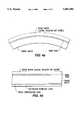
- FIG. 4cgraphically illustrates the warpage (in mils) of a 4-inch bonded wafer with a device layer thickness of about 20 ⁇ m and a bottom oxide thickness of 4 ⁇ m as a function of the thickness difference. Note that FIG. 4c includes both positive and negative thickness differences which correspond to the bottom oxide being thicker and thinner than the backside oxide, respectively. For the positive thickness differences the bonded wafer had convex warpage as in FIG. 4a.
- Protection of the stress compensation backside oxide 346 of the first methodcan also be achieved by coating the oxide with a layer of material such as silicon nitride which is not removed by processes to which the back side is exposed until all warpage sensitive process steps have been completed.
- the oxide 346 thicknessmay be adjusted so that the combined stress of the oxide and its permanent protective layer (such as nitride) match the stress of the bottom oxide 306.
- nitridenitride
- the backside oxide 346could be completely replaced by nitride, although this would require the oxide and nitride formations be controllable to produce at least approximately matching stressed layers.
- the thicknesses of the bottom oxide and a backside nitridecould be almost invariant throughout the processing.
- Another way to protect stress compensation oxide layer 346 of the first methodis to coat backside oxide 346 with photoresist prior to a wet etch and remove it after the wet etch. This can protect backside oxide 346 and keep its thickness comparable to that of bottom oxide 306 to prevent warpage. Once devices and interconnections have been formed in islands 322,323, . . . and other warpage sensitive steps completed, then backside oxide 346 can be removed.
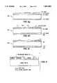
- FIGS. 5a-ishow in cross sectional elevation view a fourth preferred embodiment method of warpage control in bonded wafer processing.
- the bonded wafer processingproceeds as follow:
- Wafer 502is the device wafer and wafer 504 is the handle wafer.
- Device wafer 502has lightly doped device epilayer 510 of thickness about 35 ⁇ m and heavily doped etchstop layer 512.
- Device epilayer 510has only a native oxide on its surface.
- Handle wafer 504has 4 ⁇ m thick oxides 520 and 522 on its surfaces; oxide 520 will become the bottom oxide in the final bonded wafer, and oxide 522 will just be a backside oxide. For high voltage products the bottom oxide must be several ⁇ m thick. These oxides may be formed simultaneously such as by thermal oxidation in steam.
- Oxides 520 and 522have the same compression/tension and thus provide balanced stresses on handle wafer 504 and will deter warpage of the bonded wafer. Indeed, the purpose of backside oxide 522 is warpage deterrence by providing a stress approximately balancing that of bottom oxide 520.
- FIG. 5aalso shows a drop 530 of water plus hydrogen peroxide which are silicon oxidizers.
- bottom oxide 520thickens based on the amount of oxidizer in drop 530 and typically ends up being about 4 ⁇ m thick. Ideally, the thicknesses of bottom oxide 520 and backside oxide 522 remain roughly equal. See FIG. 5b. Also, the growth of bottom oxide 520 consumes a portion of device epilayer 510. Typically, device epilayer 510 has a final thickness of about 35 ⁇ m.
- (d)Form isolation trenches in device epilayer 510 by plasma etching with an oxide etch mask. This proceeds by first forming an oxide coating on device epilayer 510, patterning photoresist on the oxide coating, etching the oxide using the patterned photoresist as etch mask, and then etching device epilayer 510 using the etched oxide as etch mask. Thus, first thermally oxidize device epilayer 510 to form oxide 514 of thickness 4 ⁇ m. This oxidation also increases the thickness of oxide 522 to about 4.5 ⁇ m, although the growth is parabolic and not nearly so fast as that of oxide 514 due to the existing thickness of oxide 522.
- FIG. 5dshows bonded wafer 500 after this oxidation.
- bonded wafer 500Place bonded wafer 500 on a vacuum chuck and spin on photoresist and harden the photoresist. Then place the photoresist-covered wafer on an aligner vacuum chuck in a projection aligner and expose the photoresist to the trench isolation pattern. If bonded wafer 500 were warped on the magnitude of 5 mils deviation from flat at the center, then a vacuum chuck may be unable to hold the wafer down and the photoresist application or patterning may be impossible to perform. However, for bonded wafer 500 the thickness of bottom oxide 520 differs from the thickness of backside oxide 522 by only about 0.5 ⁇ m, and this keeps the warpage of bonded wafer 500 within tolerable limits.
- Oxides 520 and 522are both compressive and under similar stress, then bottom oxide 520 being thicker than backside oxide 522 implies a warpage as shown (exaggerated) in FIG. 5e.
- FIG. 5ealso heuristically indicates vacuum chuck 550 and the direction of vacuum pull.
- bottom oxide 520were thinner than backside oxide 522, then the warpage would be as shown in FIG. 5f. Because a vacuum chuck pulls at the center of a wafer, warpage as in FIG. 5e can be more easily tolerated than that shown in FIG. 5f.
- backside oxide 522would suffer net removal while bottom oxide 520 would not be affected; and this would lead to a thickness differential and warpage and processing failure.
- coating backside oxide 522 with photoresist 552 prior to a wet etch and removal after the wet etchcan protect backside oxide 522 and keep its thickness comparable to that of bottom oxide 520 to prevent warpage. See FIG. 5i. Once devices and interconnections have been formed in islands 511 and other warpage sensitive steps completed, then the backside oxide 522 can be removed.
- the stress compensation layercan be used without protection. This occurs when the thickness removed in subsequent process steps is small enough that the remaining part of the stress compensation layer keeps warpage within acceptable limits during all warpage sensitive processing steps. Thus in any of the methods the protection could be foregone in all steps following some cutoff step.
- Warpage in bonded wafersmay also be reduced by breaking up the sheet of bottom oxide which extends across the entire surface of the handle wafer. When broken up in small areas, the stress is reduced because there is less stressed oxide present and the oxide that is present may relax by expanding into the edges of non-oxide areas.
- the bottom oxidecan be broken up be removing it from the bottoms of the areas taken up by lateral trench isolation as shown in FIG. 6. Alternatively, or as an additional area of bottom oxide removal, the bottom oxide can be removed from the areas surrounding each circuit which are provided as areas to be cut (scribed or sawed) to separate the circuits from one another when wafer processing is complete.
- the bottom oxidecan be patterned using the following process sequence.
- Oxideis formed on the wafer to be laterally isolated after it has been thinned and otherwise processed into final form.
- the oxideis patterned and used as a silicon trench etch mask.
- the siliconis etched preferably by reactive ion etching to form trenches with nearly vertical side walls.
- the silicon etchpreferably under cuts the oxide so that the oxide mask overhangs the sides of the trenches.
- Oxide and or other insulatoris formed on the sides (and optionally the bottom) of the trenches by thermal oxidation and or conformal oxide deposition by chemical vapor deposition.
- the bottom oxideis removed by reactive ion etching with the side oxide being protected by the top oxide overhang (if present) and by the fact that the side walls are nearly vertical and the reactive ion etch process attacks horizontal surfaces only due to the direction of in motion (vertical).
- Thisis somewhat similar to forming oxide spacers on the sides of polysilicon gates.
- the process sequenceis illustrated in FIGS. 7a-e.
- the mask oxidemust be thicker than the bottom oxide to be an effective mask.
- the stress in an oxide (or other material) layer on a silicon (or other material) waferis proportional to layer thickness, thus a thicker layer will lead to more warpage. Conversely, a thicker wafer will have greater strength against bending and lead to less warpage for the same layer stress.
- increasing wafer diametersleads to incrasing wafer thicknesses for handling reasons, so 6 inch wafers will likely show less warpage than 4 inch wafers with similar stress layers.
- the vacuum chucks for 6 inch waferswill exert much greater pull on the wafer than will the chuck for a 4 inch wafer because the pull is proportional to the area of the vacuum chuck.
- the forceis proportional to the chuck area times atmospheric pressure assuming that the chuck can reduce pressure under the wafer to a small fraction of atmospheric pressure. This will also make 6 inch wafers likely easier to handle than 4 inch wafers.
- the uniform stress of a layer on a waferleads to a constant curvature warpage, so with the same wafer strength and same layer stress, and thus the same warpage curvature, a larger wafer will have a greater center deflection due to its larger size. The deflection will depend approximately quadratically on wafer diameter for small deflections.
- the preferred embodiment methodsmay be varied in many ways while retaining one or more of the features of bonded wafer processing with stress compensation backside layer during processing or with breakup of the bottom oxide for warpage control.
- the bottom oxidecould vary from 2 ⁇ m to 6 ⁇ m in thickness and accomodate devices operating up to 1000 volts.
- the thickness of the silicon islandscould vary from 10 ⁇ m to 60 ⁇ m for junction breakdown voltages of 100 to 1000 volts, although alternative approaches could provide high breakdown voltages with islands as thin as 1 ⁇ m.
- the orginal bottom oxidecould have initially been partially on both the device wafer and the handle wafer if a different bonding process were used.
- the backside oxide for stress compensationcould be formed after the bonding of the two wafers. Other materials could be used, such as bonding gallium arsenide to silicon.
Landscapes
- Engineering & Computer Science (AREA)
- Physics & Mathematics (AREA)
- Condensed Matter Physics & Semiconductors (AREA)
- General Physics & Mathematics (AREA)
- Manufacturing & Machinery (AREA)
- Computer Hardware Design (AREA)
- Microelectronics & Electronic Packaging (AREA)
- Power Engineering (AREA)
- Element Separation (AREA)
Abstract
Description
Claims (4)
Priority Applications (1)
| Application Number | Priority Date | Filing Date | Title |
|---|---|---|---|
| US08/843,302US5801084A (en) | 1992-06-17 | 1997-04-14 | Bonded wafer processing |
Applications Claiming Priority (4)
| Application Number | Priority Date | Filing Date | Title |
|---|---|---|---|
| US90020292A | 1992-06-17 | 1992-06-17 | |
| US33560094A | 1994-11-08 | 1994-11-08 | |
| US65380896A | 1996-05-28 | 1996-05-28 | |
| US08/843,302US5801084A (en) | 1992-06-17 | 1997-04-14 | Bonded wafer processing |
Related Parent Applications (1)
| Application Number | Title | Priority Date | Filing Date |
|---|---|---|---|
| US65380896AContinuation | 1992-06-17 | 1996-05-28 |
Publications (1)
| Publication Number | Publication Date |
|---|---|
| US5801084Atrue US5801084A (en) | 1998-09-01 |
Family
ID=25412130
Family Applications (2)
| Application Number | Title | Priority Date | Filing Date |
|---|---|---|---|
| US08/783,792Expired - LifetimeUS5780311A (en) | 1992-06-17 | 1997-01-15 | bonded wafer processing |
| US08/843,302Expired - LifetimeUS5801084A (en) | 1992-06-17 | 1997-04-14 | Bonded wafer processing |
Family Applications Before (1)
| Application Number | Title | Priority Date | Filing Date |
|---|---|---|---|
| US08/783,792Expired - LifetimeUS5780311A (en) | 1992-06-17 | 1997-01-15 | bonded wafer processing |
Country Status (5)
| Country | Link |
|---|---|
| US (2) | US5780311A (en) |
| EP (1) | EP0646286B1 (en) |
| JP (1) | JPH08501900A (en) |
| DE (1) | DE69332407T2 (en) |
| WO (1) | WO1993026041A1 (en) |
Cited By (56)
| Publication number | Priority date | Publication date | Assignee | Title |
|---|---|---|---|---|
| US5930652A (en)* | 1996-05-28 | 1999-07-27 | Motorola, Inc. | Semiconductor encapsulation method |
| WO1999040616A1 (en)* | 1998-02-05 | 1999-08-12 | Integration Associates, Inc. | A planar dielectrically isolated high speed pin photodiode and process for producing same |
| US6037634A (en)* | 1996-02-02 | 2000-03-14 | Mitsubishi Denki Kabushiki Kaisha | Semiconductor device with first and second elements formed on first and second portions |
| US6133071A (en)* | 1997-10-15 | 2000-10-17 | Nec Corporation | Semiconductor device with plate heat sink free from cracks due to thermal stress and process for assembling it with package |
| US6303967B1 (en) | 1998-02-05 | 2001-10-16 | Integration Associates, Inc. | Process for producing an isolated planar high speed pin photodiode |
| US6362075B1 (en)* | 1999-06-30 | 2002-03-26 | Harris Corporation | Method for making a diffused back-side layer on a bonded-wafer with a thick bond oxide |
| EP1202327A1 (en)* | 2000-10-31 | 2002-05-02 | Disco Corporation | Semiconductor device |
| US6383892B1 (en)* | 1998-08-06 | 2002-05-07 | International Business Machines Corporation | Double silicon-on-insulator device and method thereof |
| US6399427B1 (en)* | 2000-02-24 | 2002-06-04 | Advanced Micro Devices, Inc. | Formation of ultra-thin active device area on semiconductor on insulator (SOI) substrate |
| US6458619B1 (en) | 1998-02-05 | 2002-10-01 | Integration Associates, Inc. | Process for producing an isolated planar high speed pin photodiode with improved capacitance |
| US6485992B1 (en)* | 2001-07-03 | 2002-11-26 | Memc Electronic Materials, Inc. | Process for making wafers for ion implantation monitoring |
| US6548878B1 (en) | 1998-02-05 | 2003-04-15 | Integration Associates, Inc. | Method for producing a thin distributed photodiode structure |
| US6593254B2 (en)* | 1999-09-29 | 2003-07-15 | Infineon Technologies Ag | Method for clamping a semiconductor device in a manufacturing process |
| US6603916B1 (en) | 2001-07-26 | 2003-08-05 | Lightwave Microsystems Corporation | Lightwave circuit assembly having low deformation balanced sandwich substrate |
| US6690078B1 (en) | 1999-08-05 | 2004-02-10 | Integration Associates, Inc. | Shielded planar dielectrically isolated high speed pin photodiode and method for producing same |
| US6743662B2 (en)* | 2002-07-01 | 2004-06-01 | Honeywell International, Inc. | Silicon-on-insulator wafer for RF integrated circuit |
| US6753586B1 (en) | 1998-03-09 | 2004-06-22 | Integration Associates Inc. | Distributed photodiode structure having majority dopant gradient and method for making same |
| US20050026432A1 (en)* | 2001-04-17 | 2005-02-03 | Atwater Harry A. | Wafer bonded epitaxial templates for silicon heterostructures |
| US20050085049A1 (en)* | 2001-04-17 | 2005-04-21 | California Institute Of Technology | Wafer bonded virtual substrate and method for forming the same |
| DE102004048626B3 (en)* | 2004-10-06 | 2006-04-13 | X-Fab Semiconductor Foundries Ag | Oxidation process of silicon wafers to reduce mechanical stresses |
| US20060121696A1 (en)* | 2004-12-02 | 2006-06-08 | Sumco Corporation | Method for manufacturing SOI wafer |
| US7094618B2 (en) | 2000-08-25 | 2006-08-22 | Micron Technology, Inc. | Methods for marking a packaged semiconductor die including applying tape and subsequently marking the tape |
| US7123448B1 (en)* | 2000-10-13 | 2006-10-17 | Seagate Technology, Llc | Extended alumina basecoat advanced air bearing slider |
| US20060292822A1 (en)* | 2005-06-27 | 2006-12-28 | Ya-Hong Xie | Method for producing dislocation-free strained crystalline films |
| US20070001289A1 (en)* | 2005-06-30 | 2007-01-04 | Nec Electronics Corporation | Semiconductor device and method of manufacturing the same |
| WO2005060723A3 (en)* | 2003-12-02 | 2007-01-18 | California Inst Of Techn | Wafer bonded epitaxial templates for silicon heterostructures |
| US7169685B2 (en)* | 2002-02-25 | 2007-01-30 | Micron Technology, Inc. | Wafer back side coating to balance stress from passivation layer on front of wafer and be used as die attach adhesive |
| US20070023881A1 (en)* | 2005-06-28 | 2007-02-01 | Helmut Strack | Semiconductor Wafer with a Wiring Structure, a Semiconductor Component, and Methods for Their Production |
| US20070131734A1 (en)* | 2005-12-07 | 2007-06-14 | Khalil Hosseini | Method for the planar joining of components of semiconductor devices and a diffusion joining structure |
| EP1800171A1 (en)* | 2004-09-27 | 2007-06-27 | Idc, Llc | System and method for providing thermal compensation for an interferometric modulator display |
| US20080130089A1 (en)* | 1994-05-05 | 2008-06-05 | Idc, Llc | METHOD OF FABRICATING MEMS DEVICES (SUCH AS IMod) COMPRISING USING A GAS PHASE ETCHANT TO REMOVE A LAYER |
| US20090014844A1 (en)* | 2007-07-12 | 2009-01-15 | Lee Choong-Ho | Semiconductor device and method of manufacturing the same |
| US20090074646A1 (en)* | 2007-09-14 | 2009-03-19 | Qualcomm Mems Technologies, Inc. | Etching processes used in mems production |
| US20090315567A1 (en)* | 2006-02-22 | 2009-12-24 | Qualcomm Mems Technologies, Inc. | Electrical conditioning of mems device and insulating layer thereof |
| US20090323168A1 (en)* | 2002-09-20 | 2009-12-31 | Idc, Llc | Electromechanical devices and methods of fabricating same |
| US20100062611A1 (en)* | 2008-09-05 | 2010-03-11 | Taiwan Semiconductor Manufacturing Company, Ltd. | Method and Apparatus for Thinning a Substrate |
| US20100202038A1 (en)* | 2006-12-20 | 2010-08-12 | Qualcomm Mems Technologies, Inc. | Mems device and interconnects for same |
| US20100265563A1 (en)* | 2005-08-19 | 2010-10-21 | Qualcomm Mems Technologies, Inc. | Electromechanical device configured to minimize stress-related deformation and methods for fabricating same |
| US20110051224A1 (en)* | 2008-06-05 | 2011-03-03 | Qualcomm Mems Technologies, Inc. | Low temperature amorphous silicon sacrificial layer for controlled adhesion in mems devices |
| US20110108097A1 (en)* | 2009-11-06 | 2011-05-12 | Alliance For Sustainable Energy, Llc | Methods of manipulating stressed epistructures |
| US7952789B2 (en) | 2006-03-02 | 2011-05-31 | Qualcomm Mems Technologies, Inc. | MEMS devices with multi-component sacrificial layers |
| US8064124B2 (en) | 2006-01-18 | 2011-11-22 | Qualcomm Mems Technologies, Inc. | Silicon-rich silicon nitrides as etch stops in MEMS manufacture |
| US8115988B2 (en) | 2004-07-29 | 2012-02-14 | Qualcomm Mems Technologies, Inc. | System and method for micro-electromechanical operation of an interferometric modulator |
| US8149497B2 (en) | 2005-07-22 | 2012-04-03 | Qualcomm Mems Technologies, Inc. | Support structure for MEMS device and methods therefor |
| US20120146024A1 (en)* | 2010-12-13 | 2012-06-14 | David Lysacek | Method of forming a gettering structure and the structure therefor |
| US8278726B2 (en) | 2002-09-20 | 2012-10-02 | Qualcomm Mems Technologies, Inc. | Controlling electromechanical behavior of structures within a microelectromechanical systems device |
| US8284475B2 (en) | 2007-05-11 | 2012-10-09 | Qualcomm Mems Technologies, Inc. | Methods of fabricating MEMS with spacers between plates and devices formed by same |
| US8394656B2 (en) | 2005-12-29 | 2013-03-12 | Qualcomm Mems Technologies, Inc. | Method of creating MEMS device cavities by a non-etching process |
| US8440532B2 (en) | 2010-07-27 | 2013-05-14 | International Business Machines Corporation | Structure and method for making metal semiconductor field effect transistor (MOSFET) with isolation last process |
| US8535544B2 (en) | 2010-07-26 | 2013-09-17 | International Business Machines Corporation | Structure and method to form nanopore |
| US8928967B2 (en) | 1998-04-08 | 2015-01-06 | Qualcomm Mems Technologies, Inc. | Method and device for modulating light |
| US8927334B2 (en) | 2012-09-25 | 2015-01-06 | International Business Machines Corporation | Overcoming chip warping to enhance wetting of solder bumps and flip chip attaches in a flip chip package |
| US8971675B2 (en) | 2006-01-13 | 2015-03-03 | Qualcomm Mems Technologies, Inc. | Interconnect structure for MEMS device |
| US9110289B2 (en) | 1998-04-08 | 2015-08-18 | Qualcomm Mems Technologies, Inc. | Device for modulating light with multiple electrodes |
| US9997348B2 (en) | 2016-09-28 | 2018-06-12 | International Business Machines Corporation | Wafer stress control and topography compensation |
| CN111276542A (en)* | 2020-02-17 | 2020-06-12 | 中芯集成电路制造(绍兴)有限公司 | Trench MOS device and method of making the same |
Families Citing this family (52)
| Publication number | Priority date | Publication date | Assignee | Title |
|---|---|---|---|---|
| EP0553775B1 (en)* | 1992-01-28 | 1998-04-08 | Canon Kabushiki Kaisha | Method of manufacturing a semiconductor device |
| JP2526786B2 (en)* | 1993-05-22 | 1996-08-21 | 日本電気株式会社 | Semiconductor device and manufacturing method thereof |
| WO1996020497A1 (en)* | 1994-12-23 | 1996-07-04 | Philips Electronics N.V. | Method of manufacturing semiconductor devices with semiconductor elements formed in a layer of semiconductor material glued on a support wafer |
| DE19538005A1 (en)* | 1995-10-12 | 1997-04-17 | Fraunhofer Ges Forschung | Method of creating trench isolation in a substrate |
| US6815774B1 (en)* | 1998-10-29 | 2004-11-09 | Mitsubishi Materials Silicon Corporation | Dielectrically separated wafer and method of the same |
| US6693033B2 (en) | 2000-02-10 | 2004-02-17 | Motorola, Inc. | Method of removing an amorphous oxide from a monocrystalline surface |
| US6392257B1 (en) | 2000-02-10 | 2002-05-21 | Motorola Inc. | Semiconductor structure, semiconductor device, communicating device, integrated circuit, and process for fabricating the same |
| JP2004503920A (en) | 2000-05-31 | 2004-02-05 | モトローラ・インコーポレイテッド | Semiconductor device and method of manufacturing the semiconductor device |
| WO2002009187A2 (en) | 2000-07-24 | 2002-01-31 | Motorola, Inc. | Heterojunction tunneling diodes and process for fabricating same |
| FR2812451B1 (en)* | 2000-07-28 | 2003-01-10 | St Microelectronics Sa | METHOD FOR MANUFACTURING A SILICON-ON-INSULATION ASSEMBLY WITH THIN ISLANDS SEMICONDUCTORS SURROUNDED BY AN INSULATING MATERIAL |
| US6638838B1 (en) | 2000-10-02 | 2003-10-28 | Motorola, Inc. | Semiconductor structure including a partially annealed layer and method of forming the same |
| EP1217656A1 (en)* | 2000-12-20 | 2002-06-26 | STMicroelectronics S.r.l. | Process for manufacturing components in a semiconductor material with reduction in the starting wafer thickness |
| US20020096683A1 (en) | 2001-01-19 | 2002-07-25 | Motorola, Inc. | Structure and method for fabricating GaN devices utilizing the formation of a compliant substrate |
| US6673646B2 (en) | 2001-02-28 | 2004-01-06 | Motorola, Inc. | Growth of compound semiconductor structures on patterned oxide films and process for fabricating same |
| WO2002082551A1 (en) | 2001-04-02 | 2002-10-17 | Motorola, Inc. | A semiconductor structure exhibiting reduced leakage current |
| US6709989B2 (en) | 2001-06-21 | 2004-03-23 | Motorola, Inc. | Method for fabricating a semiconductor structure including a metal oxide interface with silicon |
| US6992321B2 (en) | 2001-07-13 | 2006-01-31 | Motorola, Inc. | Structure and method for fabricating semiconductor structures and devices utilizing piezoelectric materials |
| US6646293B2 (en) | 2001-07-18 | 2003-11-11 | Motorola, Inc. | Structure for fabricating high electron mobility transistors utilizing the formation of complaint substrates |
| US6693298B2 (en) | 2001-07-20 | 2004-02-17 | Motorola, Inc. | Structure and method for fabricating epitaxial semiconductor on insulator (SOI) structures and devices utilizing the formation of a compliant substrate for materials used to form same |
| US7019332B2 (en) | 2001-07-20 | 2006-03-28 | Freescale Semiconductor, Inc. | Fabrication of a wavelength locker within a semiconductor structure |
| US6855992B2 (en) | 2001-07-24 | 2005-02-15 | Motorola Inc. | Structure and method for fabricating configurable transistor devices utilizing the formation of a compliant substrate for materials used to form the same |
| US6667196B2 (en) | 2001-07-25 | 2003-12-23 | Motorola, Inc. | Method for real-time monitoring and controlling perovskite oxide film growth and semiconductor structure formed using the method |
| US6639249B2 (en) | 2001-08-06 | 2003-10-28 | Motorola, Inc. | Structure and method for fabrication for a solid-state lighting device |
| US6589856B2 (en) | 2001-08-06 | 2003-07-08 | Motorola, Inc. | Method and apparatus for controlling anti-phase domains in semiconductor structures and devices |
| US20030034491A1 (en) | 2001-08-14 | 2003-02-20 | Motorola, Inc. | Structure and method for fabricating semiconductor structures and devices for detecting an object |
| US6673667B2 (en) | 2001-08-15 | 2004-01-06 | Motorola, Inc. | Method for manufacturing a substantially integral monolithic apparatus including a plurality of semiconductor materials |
| EP1302984A1 (en)* | 2001-10-09 | 2003-04-16 | STMicroelectronics S.r.l. | Protection structure against electrostatic discharges (ESD) for an electronic device integrated on a SOI substrate and corresponding integration process |
| US20030071327A1 (en) | 2001-10-17 | 2003-04-17 | Motorola, Inc. | Method and apparatus utilizing monocrystalline insulator |
| US6555444B1 (en)* | 2002-01-16 | 2003-04-29 | Intel Corporation | Device and method for core buildup using a separator |
| US6916717B2 (en) | 2002-05-03 | 2005-07-12 | Motorola, Inc. | Method for growing a monocrystalline oxide layer and for fabricating a semiconductor device on a monocrystalline substrate |
| US6887793B2 (en)* | 2002-05-29 | 2005-05-03 | Taiwan Semiconductor Manufacturing Co., Ltd | Method for plasma etching a wafer after backside grinding |
| US7169619B2 (en) | 2002-11-19 | 2007-01-30 | Freescale Semiconductor, Inc. | Method for fabricating semiconductor structures on vicinal substrates using a low temperature, low pressure, alkaline earth metal-rich process |
| US6885065B2 (en) | 2002-11-20 | 2005-04-26 | Freescale Semiconductor, Inc. | Ferromagnetic semiconductor structure and method for forming the same |
| US6815234B2 (en)* | 2002-12-31 | 2004-11-09 | Infineon Technologies Aktiengesellschaft | Reducing stress in integrated circuits |
| US7020374B2 (en) | 2003-02-03 | 2006-03-28 | Freescale Semiconductor, Inc. | Optical waveguide structure and method for fabricating the same |
| US6965128B2 (en) | 2003-02-03 | 2005-11-15 | Freescale Semiconductor, Inc. | Structure and method for fabricating semiconductor microresonator devices |
| US7682933B1 (en)* | 2007-09-26 | 2010-03-23 | The United States Of America As Represented By The Secretary Of The Air Force | Wafer alignment and bonding |
| FR2941302B1 (en) | 2009-01-19 | 2011-04-15 | Soitec Silicon On Insulator | METHOD FOR TESTING THE SUBSTRATE SUBSTRATE OF A "SEMICONDUCTOR ON INSULATION" TYPE SUBSTRATE |
| US20100314725A1 (en)* | 2009-06-12 | 2010-12-16 | Qualcomm Incorporated | Stress Balance Layer on Semiconductor Wafer Backside |
| JP2011029618A (en)* | 2009-06-25 | 2011-02-10 | Sumco Corp | Method for manufacturing simox wafer and simox wafer |
| US8330245B2 (en)* | 2010-02-25 | 2012-12-11 | Memc Electronic Materials, Inc. | Semiconductor wafers with reduced roll-off and bonded and unbonded SOI structures produced from same |
| JP5853389B2 (en)* | 2011-03-28 | 2016-02-09 | ソニー株式会社 | Semiconductor device and manufacturing method of semiconductor device. |
| EP2600389B1 (en) | 2011-11-29 | 2020-01-15 | IMEC vzw | Method for bonding semiconductor substrates |
| US9397051B2 (en) | 2013-12-03 | 2016-07-19 | Invensas Corporation | Warpage reduction in structures with electrical circuitry |
| FR3064398B1 (en)* | 2017-03-21 | 2019-06-07 | Soitec | SEMICONDUCTOR TYPE STRUCTURE ON INSULATION, ESPECIALLY FOR A FRONT-SIDE TYPE IMAGE SENSOR, AND METHOD FOR MANUFACTURING SUCH STRUCTURE |
| CN107731668B (en)* | 2017-08-31 | 2018-11-13 | 长江存储科技有限责任公司 | The method that wafer stress is compensated in the hybrid bonded techniques of 3D NAND |
| CN108649034B (en)* | 2018-05-11 | 2019-08-06 | 长江存储科技有限责任公司 | Semiconductor structures and methods of forming them |
| CN220502678U (en)* | 2019-01-16 | 2024-02-20 | 株式会社村田制作所 | Silicon substrate with cavity and cavity SOI substrate using the silicon substrate |
| TWI734318B (en)* | 2019-12-25 | 2021-07-21 | 合晶科技股份有限公司 | Method of fabricating silicon on insulator |
| US11830773B2 (en)* | 2020-02-26 | 2023-11-28 | Taiwan Semiconductor Manufacturing Co., Ltd. | Semiconductor device with isolation structures |
| CN114242766B (en)* | 2021-11-08 | 2025-05-27 | 上海新硅聚合半导体有限公司 | A composite substrate structure and a method for improving its morphology |
| CN113964024B (en)* | 2021-12-21 | 2022-06-03 | 广州粤芯半导体技术有限公司 | Method for manufacturing semiconductor device |
Citations (12)
| Publication number | Priority date | Publication date | Assignee | Title |
|---|---|---|---|---|
| JPS57170539A (en)* | 1981-04-13 | 1982-10-20 | Fujitsu Ltd | Manufacture of semiconductor device |
| JPH01215041A (en)* | 1988-02-24 | 1989-08-29 | Sony Corp | Semiconductor substrate |
| JPH01302740A (en)* | 1988-05-30 | 1989-12-06 | Toshiba Corp | Dielectric isolation semiconductor substrate |
| JPH0298047A (en)* | 1988-10-04 | 1990-04-10 | Matsushita Electric Ind Co Ltd | Cadmium negative electrode for alkaline storage batteries |
| US4985745A (en)* | 1988-01-05 | 1991-01-15 | Kabushiki Kaisha Toshiba | Substrate structure for composite semiconductor device |
| JPH0394416A (en)* | 1989-09-07 | 1991-04-19 | Sumitomo Metal Mining Co Ltd | Manufacture of soi substrate |
| EP0444943A1 (en)* | 1990-02-28 | 1991-09-04 | Shin-Etsu Handotai Company Limited | A method of manufacturing a bonded wafer |
| US5071785A (en)* | 1989-07-25 | 1991-12-10 | Shin-Etsu Handotai Co., Ltd. | Method for preparing a substrate for forming semiconductor devices by bonding warped wafers |
| EP0464837A2 (en)* | 1990-07-05 | 1992-01-08 | Kabushiki Kaisha Toshiba | Method of manufacturing semiconductor substrate using semiconductor integrated circuit having dielectric separation structure |
| EP0469583A2 (en)* | 1990-07-31 | 1992-02-05 | Kabushiki Kaisha Toshiba | Semiconductor substrate with complete dielectric isolation structure and method of making the same |
| US5113236A (en)* | 1990-12-14 | 1992-05-12 | North American Philips Corporation | Integrated circuit device particularly adapted for high voltage applications |
| US5183783A (en)* | 1990-12-28 | 1993-02-02 | Shin-Etsu Handotai Co., Ltd | Method for production of dielectric-separation substrate |
Family Cites Families (5)
| Publication number | Priority date | Publication date | Assignee | Title |
|---|---|---|---|---|
| US3966577A (en)* | 1973-08-27 | 1976-06-29 | Trw Inc. | Dielectrically isolated semiconductor devices |
| US5049968A (en)* | 1988-02-08 | 1991-09-17 | Kabushiki Kaisha Toshiba | Dielectrically isolated substrate and semiconductor device using the same |
| JPH02298047A (en)* | 1989-05-12 | 1990-12-10 | Toshiba Corp | Method for manufacturing dielectrically separated semiconductor substrate |
| JPH03129854A (en)* | 1989-10-16 | 1991-06-03 | Toshiba Corp | Manufacturing method of semiconductor device |
| US5276338A (en)* | 1992-05-15 | 1994-01-04 | International Business Machines Corporation | Bonded wafer structure having a buried insulation layer |
- 1993
- 1993-06-17WOPCT/US1993/005828patent/WO1993026041A1/enactiveIP Right Grant
- 1993-06-17JPJP6501822Apatent/JPH08501900A/enactivePending
- 1993-06-17EPEP93915402Apatent/EP0646286B1/ennot_activeExpired - Lifetime
- 1993-06-17DEDE69332407Tpatent/DE69332407T2/ennot_activeExpired - Fee Related
- 1997
- 1997-01-15USUS08/783,792patent/US5780311A/ennot_activeExpired - Lifetime
- 1997-04-14USUS08/843,302patent/US5801084A/ennot_activeExpired - Lifetime
Patent Citations (12)
| Publication number | Priority date | Publication date | Assignee | Title |
|---|---|---|---|---|
| JPS57170539A (en)* | 1981-04-13 | 1982-10-20 | Fujitsu Ltd | Manufacture of semiconductor device |
| US4985745A (en)* | 1988-01-05 | 1991-01-15 | Kabushiki Kaisha Toshiba | Substrate structure for composite semiconductor device |
| JPH01215041A (en)* | 1988-02-24 | 1989-08-29 | Sony Corp | Semiconductor substrate |
| JPH01302740A (en)* | 1988-05-30 | 1989-12-06 | Toshiba Corp | Dielectric isolation semiconductor substrate |
| JPH0298047A (en)* | 1988-10-04 | 1990-04-10 | Matsushita Electric Ind Co Ltd | Cadmium negative electrode for alkaline storage batteries |
| US5071785A (en)* | 1989-07-25 | 1991-12-10 | Shin-Etsu Handotai Co., Ltd. | Method for preparing a substrate for forming semiconductor devices by bonding warped wafers |
| JPH0394416A (en)* | 1989-09-07 | 1991-04-19 | Sumitomo Metal Mining Co Ltd | Manufacture of soi substrate |
| EP0444943A1 (en)* | 1990-02-28 | 1991-09-04 | Shin-Etsu Handotai Company Limited | A method of manufacturing a bonded wafer |
| EP0464837A2 (en)* | 1990-07-05 | 1992-01-08 | Kabushiki Kaisha Toshiba | Method of manufacturing semiconductor substrate using semiconductor integrated circuit having dielectric separation structure |
| EP0469583A2 (en)* | 1990-07-31 | 1992-02-05 | Kabushiki Kaisha Toshiba | Semiconductor substrate with complete dielectric isolation structure and method of making the same |
| US5113236A (en)* | 1990-12-14 | 1992-05-12 | North American Philips Corporation | Integrated circuit device particularly adapted for high voltage applications |
| US5183783A (en)* | 1990-12-28 | 1993-02-02 | Shin-Etsu Handotai Co., Ltd | Method for production of dielectric-separation substrate |
Non-Patent Citations (8)
| Title |
|---|
| English translation of JP 01 302740; pp. 1 14, Dec. 6, 1989.* |
| English translation of JP 01-302740; pp. 1-14, Dec. 6, 1989. |
| IEEE Transactions on Electron Devices, vol. 38, No. 7, Jul. 1991, New York U.S. pp. 1650 1654, A. Nakagawa et al., Breakdown Voltage Enhancement for Devices on thin Silicon Layer/Silicon Dioxide Film .* |
| IEEE Transactions on Electron Devices, vol. 38, No. 7, Jul. 1991, New York U.S. pp. 1650-1654, A. Nakagawa et al., "Breakdown Voltage Enhancement for Devices on thin Silicon Layer/Silicon Dioxide Film". |
| Patent Abstract of Japan, vol. 13, No. 38 (E 709) Japanese Application No. 63 237408, (Sumitomo Metal Mining Co., Ltd.) Jan. 27, 1989.* |
| Patent Abstract of Japan, vol. 13, No. 38 (E-709) Japanese Application No. 63-237408, (Sumitomo Metal Mining Co., Ltd.) Jan. 27, 1989. |
| Wolf; "Silicon Processing for the VLSI Era"; 1986; pp. 532-534. |
| Wolf; Silicon Processing for the VLSI Era ; 1986; pp. 532 534.* |
Cited By (95)
| Publication number | Priority date | Publication date | Assignee | Title |
|---|---|---|---|---|
| US8105496B2 (en) | 1994-05-05 | 2012-01-31 | Qualcomm Mems Technologies, Inc. | Method of fabricating MEMS devices (such as IMod) comprising using a gas phase etchant to remove a layer |
| US20080130089A1 (en)* | 1994-05-05 | 2008-06-05 | Idc, Llc | METHOD OF FABRICATING MEMS DEVICES (SUCH AS IMod) COMPRISING USING A GAS PHASE ETCHANT TO REMOVE A LAYER |
| US6037634A (en)* | 1996-02-02 | 2000-03-14 | Mitsubishi Denki Kabushiki Kaisha | Semiconductor device with first and second elements formed on first and second portions |
| US5930652A (en)* | 1996-05-28 | 1999-07-27 | Motorola, Inc. | Semiconductor encapsulation method |
| US6133071A (en)* | 1997-10-15 | 2000-10-17 | Nec Corporation | Semiconductor device with plate heat sink free from cracks due to thermal stress and process for assembling it with package |
| US6303967B1 (en) | 1998-02-05 | 2001-10-16 | Integration Associates, Inc. | Process for producing an isolated planar high speed pin photodiode |
| US6027956A (en)* | 1998-02-05 | 2000-02-22 | Integration Associates, Inc. | Process for producing planar dielectrically isolated high speed pin photodiode |
| WO1999040616A1 (en)* | 1998-02-05 | 1999-08-12 | Integration Associates, Inc. | A planar dielectrically isolated high speed pin photodiode and process for producing same |
| US6458619B1 (en) | 1998-02-05 | 2002-10-01 | Integration Associates, Inc. | Process for producing an isolated planar high speed pin photodiode with improved capacitance |
| US6075275A (en)* | 1998-02-05 | 2000-06-13 | Integration Associates, Inc. | Planar dielectrically isolated high speed photodiode |
| US6548878B1 (en) | 1998-02-05 | 2003-04-15 | Integration Associates, Inc. | Method for producing a thin distributed photodiode structure |
| US6753586B1 (en) | 1998-03-09 | 2004-06-22 | Integration Associates Inc. | Distributed photodiode structure having majority dopant gradient and method for making same |
| US9110289B2 (en) | 1998-04-08 | 2015-08-18 | Qualcomm Mems Technologies, Inc. | Device for modulating light with multiple electrodes |
| US8928967B2 (en) | 1998-04-08 | 2015-01-06 | Qualcomm Mems Technologies, Inc. | Method and device for modulating light |
| US6383892B1 (en)* | 1998-08-06 | 2002-05-07 | International Business Machines Corporation | Double silicon-on-insulator device and method thereof |
| US7285475B2 (en) | 1999-06-30 | 2007-10-23 | Intersil Americas Inc. | Integrated circuit having a device wafer with a diffused doped backside layer |
| US7605052B2 (en) | 1999-06-30 | 2009-10-20 | Intersil Corporation | Method of forming an integrated circuit having a device wafer with a diffused doped backside layer |
| US20060009007A1 (en)* | 1999-06-30 | 2006-01-12 | Intersil Americas Inc. | Integrated circuit having a device wafer with a diffused doped backside layer |
| US20040161905A1 (en)* | 1999-06-30 | 2004-08-19 | Intersil Americas Inc. | Integrated circuit having a device wafer with a diffused doped backside layer |
| US20080026595A1 (en)* | 1999-06-30 | 2008-01-31 | Intersil Americas Inc. | Method of forming an integrated circuit having a device wafer with a diffused doped backside layer |
| US6867495B2 (en) | 1999-06-30 | 2005-03-15 | Intersil Americas Inc. | Integrated circuit having a device wafer with a diffused doped backside layer |
| US6362075B1 (en)* | 1999-06-30 | 2002-03-26 | Harris Corporation | Method for making a diffused back-side layer on a bonded-wafer with a thick bond oxide |
| US6946364B2 (en) | 1999-06-30 | 2005-09-20 | Intersil Americas Inc. | Integrated circuit having a device wafer with a diffused doped backside layer |
| US6690078B1 (en) | 1999-08-05 | 2004-02-10 | Integration Associates, Inc. | Shielded planar dielectrically isolated high speed pin photodiode and method for producing same |
| US6593254B2 (en)* | 1999-09-29 | 2003-07-15 | Infineon Technologies Ag | Method for clamping a semiconductor device in a manufacturing process |
| US6399427B1 (en)* | 2000-02-24 | 2002-06-04 | Advanced Micro Devices, Inc. | Formation of ultra-thin active device area on semiconductor on insulator (SOI) substrate |
| US7094618B2 (en) | 2000-08-25 | 2006-08-22 | Micron Technology, Inc. | Methods for marking a packaged semiconductor die including applying tape and subsequently marking the tape |
| US7238543B2 (en) | 2000-08-25 | 2007-07-03 | Micron Technology, Inc. | Methods for marking a bare semiconductor die including applying a tape having energy-markable properties |
| US7123448B1 (en)* | 2000-10-13 | 2006-10-17 | Seagate Technology, Llc | Extended alumina basecoat advanced air bearing slider |
| EP1202327A1 (en)* | 2000-10-31 | 2002-05-02 | Disco Corporation | Semiconductor device |
| US20050085049A1 (en)* | 2001-04-17 | 2005-04-21 | California Institute Of Technology | Wafer bonded virtual substrate and method for forming the same |
| US20050026432A1 (en)* | 2001-04-17 | 2005-02-03 | Atwater Harry A. | Wafer bonded epitaxial templates for silicon heterostructures |
| US6485992B1 (en)* | 2001-07-03 | 2002-11-26 | Memc Electronic Materials, Inc. | Process for making wafers for ion implantation monitoring |
| US6603916B1 (en) | 2001-07-26 | 2003-08-05 | Lightwave Microsystems Corporation | Lightwave circuit assembly having low deformation balanced sandwich substrate |
| US7169685B2 (en)* | 2002-02-25 | 2007-01-30 | Micron Technology, Inc. | Wafer back side coating to balance stress from passivation layer on front of wafer and be used as die attach adhesive |
| US7727785B2 (en) | 2002-02-25 | 2010-06-01 | Micron Technology, Inc. | Wafer back side coating to balance stress from passivation layer on front of wafer and be used as die attach adhesive |
| US6743662B2 (en)* | 2002-07-01 | 2004-06-01 | Honeywell International, Inc. | Silicon-on-insulator wafer for RF integrated circuit |
| US20040159908A1 (en)* | 2002-07-01 | 2004-08-19 | Fathimulla Mohammed A. | Silicon-on-insulator wafer for RF integrated circuit |
| US20090323168A1 (en)* | 2002-09-20 | 2009-12-31 | Idc, Llc | Electromechanical devices and methods of fabricating same |
| US8278726B2 (en) | 2002-09-20 | 2012-10-02 | Qualcomm Mems Technologies, Inc. | Controlling electromechanical behavior of structures within a microelectromechanical systems device |
| US8368124B2 (en) | 2002-09-20 | 2013-02-05 | Qualcomm Mems Technologies, Inc. | Electromechanical devices having etch barrier layers |
| WO2005060723A3 (en)* | 2003-12-02 | 2007-01-18 | California Inst Of Techn | Wafer bonded epitaxial templates for silicon heterostructures |
| US8115988B2 (en) | 2004-07-29 | 2012-02-14 | Qualcomm Mems Technologies, Inc. | System and method for micro-electromechanical operation of an interferometric modulator |
| EP1800171A1 (en)* | 2004-09-27 | 2007-06-27 | Idc, Llc | System and method for providing thermal compensation for an interferometric modulator display |
| US7517813B2 (en) | 2004-10-06 | 2009-04-14 | X-Fab Semiconductor Foundries Ag | Two-step oxidation process for semiconductor wafers |
| US20080135985A1 (en)* | 2004-10-06 | 2008-06-12 | X-Fab Semiconductor Foundries Ag | Two-Step Oxidation Process For Semiconductor Wafers |
| DE102004048626B3 (en)* | 2004-10-06 | 2006-04-13 | X-Fab Semiconductor Foundries Ag | Oxidation process of silicon wafers to reduce mechanical stresses |
| US20060121696A1 (en)* | 2004-12-02 | 2006-06-08 | Sumco Corporation | Method for manufacturing SOI wafer |
| US7582540B2 (en)* | 2004-12-02 | 2009-09-01 | Sumco Corporation | Method for manufacturing SOI wafer |
| US7265028B2 (en) | 2005-06-27 | 2007-09-04 | The Regents Of The University Of California | Method for producing dislocation-free strained crystalline films |
| US20070128830A1 (en)* | 2005-06-27 | 2007-06-07 | The Regents Of The University Of California | Method for producing dislocation-free strained crystalline films |
| CN100541725C (en)* | 2005-06-27 | 2009-09-16 | 加利福尼亚大学董事会 | Method for manufacturing dislocation-free strain crystal thin film |
| US7262112B2 (en) | 2005-06-27 | 2007-08-28 | The Regents Of The University Of California | Method for producing dislocation-free strained crystalline films |
| US20060292822A1 (en)* | 2005-06-27 | 2006-12-28 | Ya-Hong Xie | Method for producing dislocation-free strained crystalline films |
| WO2007001299A1 (en)* | 2005-06-27 | 2007-01-04 | The Regents Of The University Of California | Method for producing dislocation-free strained crystalline films |
| KR101133871B1 (en)* | 2005-06-27 | 2012-04-06 | 더 리전트 오브 더 유니버시티 오브 캘리포니아 | Method for producing dislocation-free strained crystalline films |
| US20070023881A1 (en)* | 2005-06-28 | 2007-02-01 | Helmut Strack | Semiconductor Wafer with a Wiring Structure, a Semiconductor Component, and Methods for Their Production |
| US7344936B2 (en)* | 2005-06-28 | 2008-03-18 | Infineon Technologies Ag | Semiconductor wafer with a wiring structure, a semiconductor component, and methods for their production |
| US20070001289A1 (en)* | 2005-06-30 | 2007-01-04 | Nec Electronics Corporation | Semiconductor device and method of manufacturing the same |
| US8218229B2 (en) | 2005-07-22 | 2012-07-10 | Qualcomm Mems Technologies, Inc. | Support structure for MEMS device and methods therefor |
| US8149497B2 (en) | 2005-07-22 | 2012-04-03 | Qualcomm Mems Technologies, Inc. | Support structure for MEMS device and methods therefor |
| US20100265563A1 (en)* | 2005-08-19 | 2010-10-21 | Qualcomm Mems Technologies, Inc. | Electromechanical device configured to minimize stress-related deformation and methods for fabricating same |
| US8298847B2 (en) | 2005-08-19 | 2012-10-30 | Qualcomm Mems Technologies, Inc. | MEMS devices having support structures with substantially vertical sidewalls and methods for fabricating the same |
| US8229253B2 (en) | 2005-08-19 | 2012-07-24 | Qualcomm Mems Technologies, Inc. | Electromechanical device configured to minimize stress-related deformation and methods for fabricating same |
| US7874475B2 (en)* | 2005-12-07 | 2011-01-25 | Infineon Technologies Ag | Method for the planar joining of components of semiconductor devices and a diffusion joining structure |
| US20070131734A1 (en)* | 2005-12-07 | 2007-06-14 | Khalil Hosseini | Method for the planar joining of components of semiconductor devices and a diffusion joining structure |
| US8394656B2 (en) | 2005-12-29 | 2013-03-12 | Qualcomm Mems Technologies, Inc. | Method of creating MEMS device cavities by a non-etching process |
| US8971675B2 (en) | 2006-01-13 | 2015-03-03 | Qualcomm Mems Technologies, Inc. | Interconnect structure for MEMS device |
| US8064124B2 (en) | 2006-01-18 | 2011-11-22 | Qualcomm Mems Technologies, Inc. | Silicon-rich silicon nitrides as etch stops in MEMS manufacture |
| US7932728B2 (en) | 2006-02-22 | 2011-04-26 | Qualcomm Mems Technologies, Inc. | Electrical conditioning of MEMS device and insulating layer thereof |
| US20090315567A1 (en)* | 2006-02-22 | 2009-12-24 | Qualcomm Mems Technologies, Inc. | Electrical conditioning of mems device and insulating layer thereof |
| US7952789B2 (en) | 2006-03-02 | 2011-05-31 | Qualcomm Mems Technologies, Inc. | MEMS devices with multi-component sacrificial layers |
| US20100202038A1 (en)* | 2006-12-20 | 2010-08-12 | Qualcomm Mems Technologies, Inc. | Mems device and interconnects for same |
| US8097174B2 (en) | 2006-12-20 | 2012-01-17 | Qualcomm Mems Technologies, Inc. | MEMS device and interconnects for same |
| US8830557B2 (en) | 2007-05-11 | 2014-09-09 | Qualcomm Mems Technologies, Inc. | Methods of fabricating MEMS with spacers between plates and devices formed by same |
| US8284475B2 (en) | 2007-05-11 | 2012-10-09 | Qualcomm Mems Technologies, Inc. | Methods of fabricating MEMS with spacers between plates and devices formed by same |
| US7868467B2 (en)* | 2007-07-12 | 2011-01-11 | Samsung Electronics Co., Ltd. | Semiconductor device |
| US20110076812A1 (en)* | 2007-07-12 | 2011-03-31 | Lee Choong-Ho | Semiconductor device and method of manufacturing the same |
| US20090014844A1 (en)* | 2007-07-12 | 2009-01-15 | Lee Choong-Ho | Semiconductor device and method of manufacturing the same |
| US20090074646A1 (en)* | 2007-09-14 | 2009-03-19 | Qualcomm Mems Technologies, Inc. | Etching processes used in mems production |
| US8358458B2 (en) | 2008-06-05 | 2013-01-22 | Qualcomm Mems Technologies, Inc. | Low temperature amorphous silicon sacrificial layer for controlled adhesion in MEMS devices |
| US20110051224A1 (en)* | 2008-06-05 | 2011-03-03 | Qualcomm Mems Technologies, Inc. | Low temperature amorphous silicon sacrificial layer for controlled adhesion in mems devices |
| US20100062611A1 (en)* | 2008-09-05 | 2010-03-11 | Taiwan Semiconductor Manufacturing Company, Ltd. | Method and Apparatus for Thinning a Substrate |
| US8048807B2 (en)* | 2008-09-05 | 2011-11-01 | Taiwan Semiconductor Manufacturing Company, Ltd. | Method and apparatus for thinning a substrate |
| US20110108097A1 (en)* | 2009-11-06 | 2011-05-12 | Alliance For Sustainable Energy, Llc | Methods of manipulating stressed epistructures |
| US8691663B2 (en)* | 2009-11-06 | 2014-04-08 | Alliance For Sustainable Energy, Llc | Methods of manipulating stressed epistructures |
| US8535544B2 (en) | 2010-07-26 | 2013-09-17 | International Business Machines Corporation | Structure and method to form nanopore |
| US9057719B2 (en) | 2010-07-26 | 2015-06-16 | International Business Machines Corporation | Fluidic structure with nanopore array |
| US8440532B2 (en) | 2010-07-27 | 2013-05-14 | International Business Machines Corporation | Structure and method for making metal semiconductor field effect transistor (MOSFET) with isolation last process |
| US8846500B2 (en)* | 2010-12-13 | 2014-09-30 | Semiconductor Components Industries, Llc | Method of forming a gettering structure having reduced warpage and gettering a semiconductor wafer therewith |
| US20120146024A1 (en)* | 2010-12-13 | 2012-06-14 | David Lysacek | Method of forming a gettering structure and the structure therefor |
| US8927334B2 (en) | 2012-09-25 | 2015-01-06 | International Business Machines Corporation | Overcoming chip warping to enhance wetting of solder bumps and flip chip attaches in a flip chip package |
| US9997348B2 (en) | 2016-09-28 | 2018-06-12 | International Business Machines Corporation | Wafer stress control and topography compensation |
| CN111276542A (en)* | 2020-02-17 | 2020-06-12 | 中芯集成电路制造(绍兴)有限公司 | Trench MOS device and method of making the same |
| CN111276542B (en)* | 2020-02-17 | 2022-08-09 | 绍兴中芯集成电路制造股份有限公司 | Groove type MOS device and manufacturing method thereof |
Also Published As
| Publication number | Publication date |
|---|---|
| DE69332407T2 (en) | 2003-06-18 |
| US5780311A (en) | 1998-07-14 |
| DE69332407D1 (en) | 2002-11-21 |
| JPH08501900A (en) | 1996-02-27 |
| EP0646286B1 (en) | 2002-10-16 |
| EP0646286A1 (en) | 1995-04-05 |
| WO1993026041A1 (en) | 1993-12-23 |
Similar Documents
| Publication | Publication Date | Title |
|---|---|---|
| US5801084A (en) | Bonded wafer processing | |
| US6096433A (en) | Laminated substrate fabricated from semiconductor wafers bonded to each other without contact between insulating layer and semiconductor layer and process of fabrication thereof | |
| US5882987A (en) | Smart-cut process for the production of thin semiconductor material films | |
| US5517047A (en) | Bonded wafer processing | |
| JP2717979B2 (en) | Method of fabricating thin single crystal silicon islands on insulator | |
| US4851078A (en) | Dielectric isolation process using double wafer bonding | |
| US5710057A (en) | SOI fabrication method | |
| US5476813A (en) | Method of manufacturing a bonded semiconductor substrate and a dielectric isolated bipolar transistor | |
| US5310451A (en) | Method of forming an ultra-uniform silicon-on-insulator layer | |
| US6211039B1 (en) | Silicon-on-insulator islands and method for their formation | |
| JPH0344419B2 (en) | ||
| JPS61296709A (en) | Manufacturing method of semiconductor device | |
| US6326285B1 (en) | Simultaneous multiple silicon on insulator (SOI) wafer production | |
| JPH06349694A (en) | Method for bonding of silicon to iii - v semiconductor material | |
| JPH0719738B2 (en) | Bonded wafer and manufacturing method thereof | |
| US5393694A (en) | Advanced process for recessed poly buffered locos | |
| US6127244A (en) | Method of manufacturing semiconductor device | |
| US5453395A (en) | Isolation technology using liquid phase deposition | |
| EP0701286B1 (en) | Silicon on insulating substrate and manufacturing method for same | |
| US5371035A (en) | Method for forming electrical isolation in an integrated circuit device | |
| USH1137H (en) | Wafer bonding technique for dielectric isolation processing | |
| US5786229A (en) | Method for providing isolation between semiconductor devices using epitaxial growth and polishing | |
| JPS59232437A (en) | Manufacture of semiconductor device | |
| JPH09260679A (en) | Semiconductor device and manufacturing method thereof | |
| KR100355870B1 (en) | Shallow trench isolation manufacturing method of semiconductor devices |
Legal Events
| Date | Code | Title | Description |
|---|---|---|---|
| STCF | Information on status: patent grant | Free format text:PATENTED CASE | |
| AS | Assignment | Owner name:INTERSIL CORPORATION, FLORIDA Free format text:ASSIGNMENT OF ASSIGNORS INTEREST;ASSIGNOR:HARRIS CORPORATION;REEL/FRAME:010247/0043 Effective date:19990813 | |
| AS | Assignment | Owner name:CREDIT SUISSE FIRST BOSTON, AS COLLATERAL AGENT, N Free format text:SECURITY INTEREST;ASSIGNOR:INTERSIL CORPORATION;REEL/FRAME:010351/0410 Effective date:19990813 | |
| FEPP | Fee payment procedure | Free format text:PAYOR NUMBER ASSIGNED (ORIGINAL EVENT CODE: ASPN); ENTITY STATUS OF PATENT OWNER: LARGE ENTITY | |
| FPAY | Fee payment | Year of fee payment:4 | |
| REMI | Maintenance fee reminder mailed | ||
| FPAY | Fee payment | Year of fee payment:8 | |
| FPAY | Fee payment | Year of fee payment:12 | |
| AS | Assignment | Owner name:MORGAN STANLEY & CO. INCORPORATED,NEW YORK Free format text:SECURITY AGREEMENT;ASSIGNORS:INTERSIL CORPORATION;TECHWELL, INC.;INTERSIL COMMUNICATIONS, INC.;AND OTHERS;REEL/FRAME:024390/0608 Effective date:20100427 | |
| AS | Assignment | Owner name:INTERSIL CORPORATION,FLORIDA Free format text:RELEASE BY SECURED PARTY;ASSIGNOR:CREDIT SUISSE FIRST BOSTON;REEL/FRAME:024445/0049 Effective date:20030306 |