US5801083A - Use of polymer spacers for the fabrication of shallow trench isolation regions with rounded top corners - Google Patents
Use of polymer spacers for the fabrication of shallow trench isolation regions with rounded top cornersDownload PDFInfo
- Publication number
- US5801083A US5801083AUS08/954,046US95404697AUS5801083AUS 5801083 AUS5801083 AUS 5801083AUS 95404697 AUS95404697 AUS 95404697AUS 5801083 AUS5801083 AUS 5801083A
- Authority
- US
- United States
- Prior art keywords
- shallow trench
- semiconductor substrate
- insulator layer
- opening
- angstroms
- Prior art date
- Legal status (The legal status is an assumption and is not a legal conclusion. Google has not performed a legal analysis and makes no representation as to the accuracy of the status listed.)
- Expired - Fee Related
Links
Images


Classifications
- H—ELECTRICITY
- H01—ELECTRIC ELEMENTS
- H01L—SEMICONDUCTOR DEVICES NOT COVERED BY CLASS H10
- H01L21/00—Processes or apparatus adapted for the manufacture or treatment of semiconductor or solid state devices or of parts thereof
- H01L21/70—Manufacture or treatment of devices consisting of a plurality of solid state components formed in or on a common substrate or of parts thereof; Manufacture of integrated circuit devices or of parts thereof
- H01L21/71—Manufacture of specific parts of devices defined in group H01L21/70
- H01L21/76—Making of isolation regions between components
- H01L21/762—Dielectric regions, e.g. EPIC dielectric isolation, LOCOS; Trench refilling techniques, SOI technology, use of channel stoppers
- H01L21/76224—Dielectric regions, e.g. EPIC dielectric isolation, LOCOS; Trench refilling techniques, SOI technology, use of channel stoppers using trench refilling with dielectric materials
- H01L21/76232—Dielectric regions, e.g. EPIC dielectric isolation, LOCOS; Trench refilling techniques, SOI technology, use of channel stoppers using trench refilling with dielectric materials of trenches having a shape other than rectangular or V-shape, e.g. rounded corners, oblique or rounded trench walls
- Y—GENERAL TAGGING OF NEW TECHNOLOGICAL DEVELOPMENTS; GENERAL TAGGING OF CROSS-SECTIONAL TECHNOLOGIES SPANNING OVER SEVERAL SECTIONS OF THE IPC; TECHNICAL SUBJECTS COVERED BY FORMER USPC CROSS-REFERENCE ART COLLECTIONS [XRACs] AND DIGESTS
- Y10—TECHNICAL SUBJECTS COVERED BY FORMER USPC
- Y10S—TECHNICAL SUBJECTS COVERED BY FORMER USPC CROSS-REFERENCE ART COLLECTIONS [XRACs] AND DIGESTS
- Y10S148/00—Metal treatment
- Y10S148/05—Etch and refill
- Y—GENERAL TAGGING OF NEW TECHNOLOGICAL DEVELOPMENTS; GENERAL TAGGING OF CROSS-SECTIONAL TECHNOLOGIES SPANNING OVER SEVERAL SECTIONS OF THE IPC; TECHNICAL SUBJECTS COVERED BY FORMER USPC CROSS-REFERENCE ART COLLECTIONS [XRACs] AND DIGESTS
- Y10—TECHNICAL SUBJECTS COVERED BY FORMER USPC
- Y10S—TECHNICAL SUBJECTS COVERED BY FORMER USPC CROSS-REFERENCE ART COLLECTIONS [XRACs] AND DIGESTS
- Y10S148/00—Metal treatment
- Y10S148/161—Tapered edges
- Y—GENERAL TAGGING OF NEW TECHNOLOGICAL DEVELOPMENTS; GENERAL TAGGING OF CROSS-SECTIONAL TECHNOLOGIES SPANNING OVER SEVERAL SECTIONS OF THE IPC; TECHNICAL SUBJECTS COVERED BY FORMER USPC CROSS-REFERENCE ART COLLECTIONS [XRACs] AND DIGESTS
- Y10—TECHNICAL SUBJECTS COVERED BY FORMER USPC
- Y10S—TECHNICAL SUBJECTS COVERED BY FORMER USPC CROSS-REFERENCE ART COLLECTIONS [XRACs] AND DIGESTS
- Y10S438/00—Semiconductor device manufacturing: process
- Y10S438/978—Semiconductor device manufacturing: process forming tapered edges on substrate or adjacent layers
Definitions
- the present inventionrelates to a method of forming isolation regions, for semiconductor devices, and more specifically to a method of creating an insulator filled shallow trench, with rounded top corners and minimized top corner wraparound.
- the semiconductor industryis continually striving to improve performance of semiconductor products, while still reducing or maintaining the cost of these same semiconductor products. These objectives have been successfully addressed via micro-miniaturization, or the ability to fabricate semiconductor devices using sub-micron features.
- the smaller device featuresresult in reductions in performance degrading resistances and capacitances, while also allowing levels of integration, previously obtained only with larger counterparts, now able to be realized with smaller semiconductor chips.
- the use of smaller chipsresults in more semiconductor chips to be realized from a specific size starting substrate, thus reducing the manufacturing costs for a specific semiconductor chip.
- Micro-miniaturizationhas been accomplished via advances in specific semiconductor fabrication disciplines, such as photolithography and dry etching.
- semiconductor fabrication disciplinessuch as photolithography and dry etching.
- the use of more advanced exposure tools, as well as the development of more sensitive photoresist materials,have allowed sub-micron images in photoresist layers to be routinely obtained.
- Similar advances in the dry etching disciplinehave allow the successful the sub-micron images in photoresist layers to be successfully transferred to underlying materials, used for the fabrication of semiconductor devices.
- semiconductor deviceshave benefitted from structural enhancements, such as the use of insulator filled, shallow trench isolation, (STI), regions.
- STI regionsused for isolation between specific device elements or device regions, consumes less area, then previously used, thermally grown, field oxide, (FOX), regions.
- This inventionwill describe a process for forming STI regions, with rounded corners, thus decreasing the risk of leakage related yield losses.
- the rounded cornersare obtained via formation of a polymer layer, during an initial phase of the STI patterning procedure, first resulting in a sharp cornered, silicon shape, exposed between masking layers and a shallow trench.
- a subsequent oxidation procedureconverts the sharp cornered silicon shape, exposed only between masking layers, and a shallow trench, to a rounded cornered, silicon shape.
- Prior artsuch as Giammarco, et al, in U.S. Pat. No. 4,707,218, describe the use of a polymer layer, on the side of an opening in a photoresist shape, decreasing the dimension of the opening.
- the reduced opening imageis then transferred to an underlying material via anisotropic, reactive ion etching, (RIE), procedures.
- RIEreactive ion etching
- a photoresist shapeis used as a mask to create an opening in a silicon nitride layer, and an underlying pad oxide layer, on a semiconductor substrate, via anisotropic reactive ion etching procedures.
- a polymer spaceris formed on the exposed sides of the opening in the photoresist shape, the silicon nitride layer, and the pad oxide layer. Shallow trenches are formed in the semiconductor substrate, via dry etching procedures, using the polymer coated opening as a mask.
- a thermal oxidation procedureis used to form a shallow trench oxide liner layer, on the exposed shallow trench surfaces, and on the unetched silicon, converting the sharp corner, at the unetched silicon--shallow trench intersection, to a rounded corner.
- Filling of the shallow trenches with insulator materialis followed by removal of unwanted insulator material, on the top surface of the masking silicon nitride layer, via chemical mechanical polishing procedures.
- FIGS. 1-8which schematically, in cross-sectional style, show the stages of fabrication used to create insulator filled, shallow trench isolation regions, with rounded corners.
- STI regionscan be used to provide the needed isolation for metal oxide semiconductor field effect transistor, (MOSFET), such as N channel, (NFET), P channel, (PFET), complimentary, (CMOS), or BiCMOS devices.
- MOSFETmetal oxide semiconductor field effect transistor
- a semiconductor substrate 1, comprised of single crystalline silicon, with a ⁇ 100> crystallographic orientationis used, and shown schematically in FIG. 1.
- a pad oxide layer 2, of silicon oxideis formed on semiconductor substrate 1, at a thickness between about 50 to 200 Angstroms, via thermal oxidation procedures.
- a silicon nitride layer 3,is next deposited, using either low pressure chemical vapor deposition, (LPCVD), or plasma enhanced chemical vapor deposition, (PECVD), procedures, to a thickness between about 1000 to 2000 Angstroms.
- photoresist shape 4 with opening 5ais formed on silicon nitride layer 3, with opening 5a, being greater than 2000 Angstroms.
- An anisotropic RIE procedureusing CF 4 --CHF 3 --Ar as an etchant for silicon nitride layer 3, and using CHF 3 --CF 4 --Ar--CO as an etchant for pad oxide layer 2, is used to transfer opening 5a, in photoresist layer 4, to the underlying insulator layers.
- a thin polymer layer 6ais formed on the top of photoresist shape 4, as well as on the sides of opening 5a.
- the thickness of polymer layer 6a, on the sides of opening 5ais thicker at the top than at the bottom of opening 5a, with the thickness of polymer layer 6a, only between about 25 to 50 Angstroms on the sides of the bottom of opening 5a.
- a thicker polymer layer 6b, or polymer spacer,is next formed on the exposed sides of opening 5a, forming opening 5b.
- Polymer layer 6bconsisting of fluorinated hydrocarbons, is formed during an over etch cycle, after the completion of opening 5a, using CHF 3 --CF 4 --Ar--CO.
- Polymer layer 6b, or polymer spacers, formed on the sides of opening 5ahave a thickness between about 200 to 500 Angstroms, while polymer layer 6, on the top surface of photoresist shape 4, and on the exposed surface of semiconductor substrate 1, in opening 5b, is thinner, resulting from the exposure of these surfaces to the ion bombardment experienced during the over etch cycle. This is schematically shown in FIG. 2.
- a shallow trench 7,is next formed in semiconductor substrate 1, via a RIE procedure, using either HBr--Cl 2 --O 2 , or Cl 2 --O 2 , as an etchant, to a depth between about 1500 to 4000 Angstroms.
- the "sloped" or “tapered” trench, exhibiting a profile angle between about 70° to 90°,is controlled by the etching conditions used such as gas ratio, pressure, and bias. This is schematically shown in FIG. 3.
- Photoresist shape 4, as well as polymer layer 6b,are removed via plasma oxygen ashing procedures, resulting in the shallow trench schematically shown in FIG. 4.
- the width of the region of unetched semiconductor substrateis equal to the thickness of the polymer spacers, between about 200 to 500 Angstroms, that previously existed on the sides of opening 5a.
- Sharp corner 8acan present a point of high stress, resulting in possible yield and reliability problems, for the completed devices.
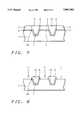
- FIG. 5The result of a procedure used to reduce the severity of the sharp corner 8a, is schematically shown in FIG. 5.
- the top corner 8ais now converted to a rounded corner 8b, reducing the stress at this interface.
- Silicon oxide layer 10is obtained via use of either LPCVD, sub-atmospheric pressure chemical vapor deposition, (SACVD), high density plasma chemical vapor deposition, (HDPCVD), or atmospheric pressure chemical vapor deposition, (APCVD), procedures, using tetraethylorthosilicate, (TEOS), or silane and oxygen, as a source, to a thickness between about 4000 to 7000 Angstroms. This is schematically shown in FIG. 6. Removal of unwanted silicon oxide layer 10, on the top surface of silicon nitride layer 3, is removed via chemical mechanical polishing procedures, using silicon nitride layer 3, as a stop layer.
- SACVDsub-atmospheric pressure chemical vapor deposition
- HDPCVDhigh density plasma chemical vapor deposition
- APCVDatmospheric pressure chemical vapor deposition
- Silicon nitride layer 3is then removed using a hot phosphoric acid solution, followed by a buffered hydrofluoric acid procedure, used to remove pad oxide layer 2.
- These wet etch proceduresresult in the STI structure, comprised of shallow trenches, in semiconductor substrate 1, with rounded corners 8b, filled with silicon oxide layer 10. This is schematically shown in FIG. 8. Regions 11, located between STI structures, can now be used to fabricate the desired MOSFET devices.
Landscapes
- Engineering & Computer Science (AREA)
- Physics & Mathematics (AREA)
- Condensed Matter Physics & Semiconductors (AREA)
- General Physics & Mathematics (AREA)
- Manufacturing & Machinery (AREA)
- Computer Hardware Design (AREA)
- Microelectronics & Electronic Packaging (AREA)
- Power Engineering (AREA)
- Element Separation (AREA)
Abstract
Description
Claims (16)
Priority Applications (2)
| Application Number | Priority Date | Filing Date | Title |
|---|---|---|---|
| US08/954,046US5801083A (en) | 1997-10-20 | 1997-10-20 | Use of polymer spacers for the fabrication of shallow trench isolation regions with rounded top corners |
| SG1998000902ASG65753A1 (en) | 1997-10-20 | 1998-04-30 | Use of polmer spaces for the fabrication of shallow trench isolation regions with rounded top corners |
Applications Claiming Priority (1)
| Application Number | Priority Date | Filing Date | Title |
|---|---|---|---|
| US08/954,046US5801083A (en) | 1997-10-20 | 1997-10-20 | Use of polymer spacers for the fabrication of shallow trench isolation regions with rounded top corners |
Publications (1)
| Publication Number | Publication Date |
|---|---|
| US5801083Atrue US5801083A (en) | 1998-09-01 |
Family
ID=25494868
Family Applications (1)
| Application Number | Title | Priority Date | Filing Date |
|---|---|---|---|
| US08/954,046Expired - Fee RelatedUS5801083A (en) | 1997-10-20 | 1997-10-20 | Use of polymer spacers for the fabrication of shallow trench isolation regions with rounded top corners |
Country Status (2)
| Country | Link |
|---|---|
| US (1) | US5801083A (en) |
| SG (1) | SG65753A1 (en) |
Cited By (127)
| Publication number | Priority date | Publication date | Assignee | Title |
|---|---|---|---|---|
| US5891771A (en)* | 1997-12-22 | 1999-04-06 | Taiwan Semiconductor Manufacturing Company, Ltd. | Recessed structure for shallow trench isolation and salicide process |
| US5933749A (en)* | 1997-10-27 | 1999-08-03 | United Microelectronics Corp. | Method for removing a top corner of a trench |
| US5937309A (en)* | 1998-11-23 | 1999-08-10 | United Semiconductor Corp. | Method for fabricating shallow trench isolation structure |
| US5945352A (en)* | 1997-12-19 | 1999-08-31 | Advanced Micro Devices | Method for fabrication of shallow isolation trenches with sloped wall profiles |
| US5963819A (en)* | 1998-01-26 | 1999-10-05 | United Silicon Incorporated | Method of fabricating shallow trench isolation |
| US5966615A (en)* | 1992-12-10 | 1999-10-12 | Micron Technology, Inc. | Method of trench isolation using spacers to form isolation trenches with protected corners |
| US5976948A (en)* | 1998-02-19 | 1999-11-02 | Advanced Micro Devices | Process for forming an isolation region with trench cap |
| US5981356A (en)* | 1997-07-28 | 1999-11-09 | Integrated Device Technology, Inc. | Isolation trenches with protected corners |
| US5994229A (en)* | 1998-01-12 | 1999-11-30 | Taiwan Semiconductor Manufacturing Company Ltd. | Achievement of top rounding in shallow trench etch |
| US6001706A (en)* | 1997-12-08 | 1999-12-14 | Chartered Semiconductor Manufacturing, Ltd. | Method for making improved shallow trench isolation for semiconductor integrated circuits |
| US6025249A (en)* | 1997-09-10 | 2000-02-15 | United Microelectronics Corp. | Method for manufacturing shallow trench isolation structure |
| US6034409A (en)* | 1997-08-28 | 2000-03-07 | Mitsubishi Denki Kabushiki Kaisha | Isolation trench having plural profile angles |
| US6037238A (en)* | 1999-01-04 | 2000-03-14 | Vanguard International Semiconductor Corporation | Process to reduce defect formation occurring during shallow trench isolation formation |
| US6051479A (en)* | 1998-06-02 | 2000-04-18 | United Semiconductor Corp. | Method of fabricating shallow trench isolation |
| US6060399A (en)* | 1997-03-18 | 2000-05-09 | Lg Semicon Co., Ltd. | Method for isolating semiconductor devices |
| US6069057A (en)* | 1998-05-18 | 2000-05-30 | Powerchip Semiconductor Corp. | Method for fabricating trench-isolation structure |
| US6074932A (en)* | 1998-01-28 | 2000-06-13 | Texas Instruments - Acer Incorporated | Method for forming a stress-free shallow trench isolation |
| US6140206A (en)* | 1999-06-14 | 2000-10-31 | Chartered Semiconductor Manufacturing Ltd. | Method to form shallow trench isolation structures |
| US6153478A (en)* | 1998-01-28 | 2000-11-28 | United Microelectronics Corp. | STI process for eliminating kink effect |
| US6159822A (en)* | 1999-06-02 | 2000-12-12 | Vanguard International Semiconductor Corporation | Self-planarized shallow trench isolation |
| US6165906A (en)* | 1999-01-26 | 2000-12-26 | Advanced Micro Devices, Inc. | Semiconductor topography employing a shallow trench isolation structure with an improved trench edge |
| US6174786B1 (en)* | 1999-11-23 | 2001-01-16 | Lucent Technologies, Inc. | Shallow trench isolation method providing rounded top trench corners |
| US6180490B1 (en) | 1999-05-25 | 2001-01-30 | Chartered Semiconductor Manufacturing Ltd. | Method of filling shallow trenches |
| US6184071B1 (en)* | 1999-01-20 | 2001-02-06 | Hyundai Electronics Industries Co., Ltd. | Semiconductor device and method for fabricating the same |
| US6194284B1 (en) | 1999-08-30 | 2001-02-27 | Taiwan Semiconductor Manufacturing Company | Method for forming residue free etched silicon layer |
| US6197659B1 (en) | 1999-03-09 | 2001-03-06 | Mosel Vitelic, Inc. | Divot free shallow trench isolation process |
| US6218309B1 (en) | 1999-06-30 | 2001-04-17 | Lam Research Corporation | Method of achieving top rounding and uniform etch depths while etching shallow trench isolation features |
| US6225229B1 (en)* | 1999-05-24 | 2001-05-01 | Advanced Micro Devices, Inc. | Removable photoresist spacers in CMOS transistor fabrication |
| US6228727B1 (en)* | 1999-09-27 | 2001-05-08 | Chartered Semiconductor Manufacturing, Ltd. | Method to form shallow trench isolations with rounded corners and reduced trench oxide recess |
| US6238999B1 (en)* | 1998-09-03 | 2001-05-29 | Micron Technology | Isolation region forming methods |
| US6245639B1 (en)* | 1999-02-08 | 2001-06-12 | Taiwan Semiconductor Manufacturing Company | Method to reduce a reverse narrow channel effect for MOSFET devices |
| SG81252A1 (en)* | 1998-09-10 | 2001-06-19 | Chartered Semiconductor Mfg | A method to improve shallow trench isolation performance |
| US6251753B1 (en)* | 1999-11-23 | 2001-06-26 | Ching-Fa Yeh | Method of sidewall capping for degradation-free damascene trenches of low dielectric constant dielectric by selective liquid-phase deposition |
| US6287974B1 (en) | 1999-06-30 | 2001-09-11 | Lam Research Corporation | Method of achieving top rounding and uniform etch depths while etching shallow trench isolation features |
| US6300219B1 (en)* | 1999-08-30 | 2001-10-09 | Micron Technology, Inc. | Method of forming trench isolation regions |
| US6316815B1 (en)* | 1999-03-26 | 2001-11-13 | Vanguard International Semiconductor Corporation | Structure for isolating integrated circuits in semiconductor substrate and method for making it |
| US6322634B1 (en)* | 1997-01-27 | 2001-11-27 | Micron Technology, Inc. | Shallow trench isolation structure without corner exposure |
| US6326283B1 (en)* | 2000-03-07 | 2001-12-04 | Vlsi Technology, Inc. | Trench-diffusion corner rounding in a shallow-trench (STI) process |
| US6348396B1 (en) | 1998-03-27 | 2002-02-19 | Hitachi, Ltd. | Semiconductor device and production thereof |
| WO2002015262A1 (en)* | 2000-08-12 | 2002-02-21 | Seung Joon Kim | Method of isolating semiconductor device |
| US6355540B2 (en)* | 1998-07-27 | 2002-03-12 | Acer Semicondutor Manufacturing Inc. | Stress-free shallow trench isolation |
| US6372606B1 (en)* | 1998-08-07 | 2002-04-16 | Samsung Electronics Co., Ltd. | Method of forming isolation trenches in a semiconductor device |
| US6376383B2 (en)* | 1998-01-16 | 2002-04-23 | Nec Corporation | Method for etching silicon layer |
| US20020086543A1 (en)* | 2001-01-03 | 2002-07-04 | Trapp Shane J. | Method of forming integrated circuitry and method of forming shallow trench isolation in a semiconductor substrate |
| US20020094493A1 (en)* | 1998-04-18 | 2002-07-18 | Coming Chen | Method of forming partial reverse active mask |
| US6426300B2 (en)* | 1999-12-30 | 2002-07-30 | Hyundai Electronics Industries Co., Ltd. | Method for fabricating semiconductor device by using etching polymer |
| US6432832B1 (en) | 1999-06-30 | 2002-08-13 | Lam Research Corporation | Method of improving the profile angle between narrow and wide features |
| US20020109181A1 (en)* | 1999-04-26 | 2002-08-15 | Taiwan Semiconductor Manufacturing Company | Method to increase coupling ratio of source to floating gate in split-gate flash |
| US20020121673A1 (en)* | 2000-08-31 | 2002-09-05 | Keiji Jono | Methods of forming an isolation trench in a semiconductor, methods of forming an isolation trench in a surface of a silicon wafer, methods of forming an isolation trench-isolated transistor, trench-isolated transistor, trench isolation structures formed in a semiconductor, memory cells and DRAMs |
| US20020132483A1 (en)* | 1998-09-03 | 2002-09-19 | Moore John T. | Methods of forming materials within openings, and methods of forming isolation regions |
| US6455382B1 (en)* | 2001-05-03 | 2002-09-24 | Taiwan Semiconductor Manufacturing Co., Ltd. | Multi-step method for forming sacrificial silicon oxide layer |
| US6461937B1 (en) | 1999-01-11 | 2002-10-08 | Samsung Electronics Co., Ltd. | Methods of forming trench isolation regions having recess-inhibiting layers therein that protect against overetching |
| US6461935B2 (en)* | 1999-01-14 | 2002-10-08 | Mitsubishi Denki Kabushiki Kaisha | Method of manufacturing trench-shaped isolator |
| US6503813B1 (en) | 2000-06-16 | 2003-01-07 | International Business Machines Corporation | Method and structure for forming a trench in a semiconductor substrate |
| WO2003030185A1 (en)* | 2001-09-28 | 2003-04-10 | Candescent Intellectual Property Services, Inc. | Method for implementing an efficient and economical cathode process |
| US6555442B1 (en) | 2002-01-08 | 2003-04-29 | Taiwan Semiconductor Manufacturing Company | Method of forming shallow trench isolation with rounded corner and divot-free by using disposable spacer |
| US6566230B1 (en)* | 2001-12-27 | 2003-05-20 | Advanced Micro Devices, Inc. | Shallow trench isolation spacer for weff improvement |
| US6593189B2 (en)* | 2001-07-04 | 2003-07-15 | Kabushiki Kaisha Toshiba | Semiconductor memory reducing current consumption and narrow channel effect and method of manufacturing the same |
| US20030146489A1 (en)* | 1998-12-08 | 2003-08-07 | Mitsubishi Denki Kabushiki Kaisha | Semiconductor device and method of manufacturing the same |
| EP1052693A3 (en)* | 1999-05-13 | 2003-08-13 | STMicroelectronics, Inc. | Improved integrated-circuit isolation structure and method for forming the same |
| US6620575B2 (en)* | 1999-02-04 | 2003-09-16 | Applied Materials, Inc | Construction of built-up structures on the surface of patterned masking used for polysilicon etch |
| US6653058B2 (en)* | 1999-06-25 | 2003-11-25 | Lam Research Corporation | Methods for reducing profile variation in photoresist trimming |
| US6683354B2 (en)* | 2001-03-12 | 2004-01-27 | Samsung Electronics, Co., Ltd. | Semiconductor device having trench isolation layer and a method of forming the same |
| US20040048483A1 (en)* | 2000-06-19 | 2004-03-11 | Heon Lee | Method to etch poly Si gate stacks with raised STI structure |
| US20040067446A1 (en)* | 2002-10-02 | 2004-04-08 | Hall Eric Spencer | Ink jet printheads and methods therefor |
| KR100429421B1 (en)* | 2000-08-12 | 2004-04-29 | 김승준 | Shallow Trench Forming Method for Semiconductor Isolation |
| US6746936B1 (en)* | 2002-12-09 | 2004-06-08 | Hynix Semiconductor Inc. | Method for forming isolation film for semiconductor devices |
| US20040157395A1 (en)* | 2002-12-31 | 2004-08-12 | Yoo Seung Jong | Method for fabricating nonvolatile memory device |
| EP1069613A3 (en)* | 1999-07-16 | 2004-08-18 | Chartered Semiconductor Manufacturing Pte Ltd. | Low-leakage architecture for sub-0.18 micrometer salicided CMOS device |
| US20040266136A1 (en)* | 2003-06-30 | 2004-12-30 | Tae-Woo Jung | Method for fabricating semiconductor device having trench type device isolation layer |
| US6841453B2 (en)* | 2000-12-29 | 2005-01-11 | Stmicroelectronics S.R.L. | Process for manufacturing integrated devices having connections on a separate wafer, and integrated device thus obtained |
| US20050009368A1 (en)* | 2003-07-07 | 2005-01-13 | Vaartstra Brian A. | Methods of forming a phosphorus doped silicon dioxide comprising layer, and methods of forming trench isolation in the fabrication of integrated circuitry |
| US20050023576A1 (en)* | 2003-07-31 | 2005-02-03 | Wen-Chin Lee | Semiconductor structure having a strained region and a method of fabricating same |
| US20050054213A1 (en)* | 2003-09-05 | 2005-03-10 | Derderian Garo J. | Methods of depositing a silicon dioxide comprising layer in the fabrication of integrated circuitry, and methods of forming trench isolation in the fabrication of integrated circuitry |
| US6890859B1 (en) | 2001-08-10 | 2005-05-10 | Cypress Semiconductor Corporation | Methods of forming semiconductor structures having reduced defects, and articles and devices formed thereby |
| US20050098380A1 (en)* | 2003-09-23 | 2005-05-12 | Luscombe Terry L. | Vehicle mounted utility apparatus with quick attachment means |
| US20050142804A1 (en)* | 2003-12-30 | 2005-06-30 | Dongbuanam Semiconductor Inc. | Method for fabricating shallow trench isolation structure of semiconductor device |
| US20050158964A1 (en)* | 2004-01-20 | 2005-07-21 | Taiwan Semiconductor Manufacturing Co., Ltd. | Method of forming an STI feature to avoid electrical charge leakage |
| US20050208778A1 (en)* | 2004-03-22 | 2005-09-22 | Weimin Li | Methods of depositing silicon dioxide comprising layers in the fabrication of integrated circuitry, methods of forming trench isolation, and methods of forming arrays of memory cells |
| US20050205517A1 (en)* | 2004-03-17 | 2005-09-22 | Krawczyk John W | Method for making a micro-fluid ejection device |
| US20050221609A1 (en)* | 2004-03-31 | 2005-10-06 | Shinichi Yotsuya | Mask, method for manufacturing a mask, method for manufacturing an electro-optical device, and electronic equipment |
| US20060046426A1 (en)* | 2004-08-31 | 2006-03-02 | Micron Technology, Inc. | Methods of forming trench isolation in the fabrication of integrated circuitry, methods of fabricating memory circuitry, integrated circuitry and memory integrated circuitry |
| US20060043066A1 (en)* | 2004-08-26 | 2006-03-02 | Kamp Thomas A | Processes for pre-tapering silicon or silicon-germanium prior to etching shallow trenches |
| US7029987B2 (en)* | 2001-04-27 | 2006-04-18 | Samsung Electronics Co., Ltd. | Method of manufacturing semiconductor device having shallow trench isolation (STI) |
| US20060138484A1 (en)* | 2004-12-29 | 2006-06-29 | Dongbuanam Semiconductor Inc. | CMOS image sensor and method for fabricating the same |
| US20060183294A1 (en)* | 2005-02-17 | 2006-08-17 | Micron Technology, Inc. | Methods of forming integrated circuitry |
| US7098141B1 (en) | 2003-03-03 | 2006-08-29 | Lam Research Corporation | Use of silicon containing gas for CD and profile feature enhancements of gate and shallow trench structures |
| US20060197225A1 (en)* | 2005-03-07 | 2006-09-07 | Qi Pan | Electrically conductive line, method of forming an electrically conductive line, and method of reducing titanium silicide agglomeration in fabrication of titanium silicide over polysilicon transistor gate lines |
| US20060208336A1 (en)* | 2003-09-08 | 2006-09-21 | Wen-Chin Lee | Semiconductor structure having a strained region and a method of fabricating same |
| US20060223279A1 (en)* | 2005-04-01 | 2006-10-05 | Micron Technology, Inc. | Methods of forming trench isolation in the fabrication of integrated circuitry and methods of fabricating integrated circuitry |
| US7129148B2 (en)* | 2000-08-15 | 2006-10-31 | Seiko Epson Corporation | Methods for manufacturing semiconductor devices and semiconductor devices having trench isolation regions |
| US20060270185A1 (en)* | 2005-05-30 | 2006-11-30 | Hynix Semiconductor Inc. | Method of forming isolation film of semiconductor device |
| US20060292787A1 (en)* | 2005-06-28 | 2006-12-28 | Hongmei Wang | Semiconductor processing methods, and semiconductor constructions |
| US20070018215A1 (en)* | 2005-07-19 | 2007-01-25 | Micron Technology, Inc. | Semiconductor constructions, memory arrays, electronic systems, and methods of forming semiconductor constructions |
| US20070026599A1 (en)* | 2005-07-27 | 2007-02-01 | Advanced Micro Devices, Inc. | Methods for fabricating a stressed MOS device |
| US20070117346A1 (en)* | 2005-11-24 | 2007-05-24 | Kwak Sung H | Method for fabricating semiconductor device |
| US20070128789A1 (en)* | 2003-11-17 | 2007-06-07 | Samsung Electronics Co., Ltd. | Methods of Fabricating Semiconductor Devices with a Source/Drain Formed on a Recessed Portion of an Isolation Layer |
| US20070212874A1 (en)* | 2006-03-08 | 2007-09-13 | Micron Technology, Inc. | Method for filling shallow isolation trenches and other recesses during the formation of a semiconductor device and electronic systems including the semiconductor device |
| US20070238295A1 (en)* | 2006-04-11 | 2007-10-11 | Micron Technology, Inc. | Methods of forming semiconductor constructions |
| US7294555B2 (en) | 2002-12-20 | 2007-11-13 | Dongbu Electronics Co., Ltd. | Method of forming trench in semiconductor device using polish stop layer and anti-reflection coating |
| US20070264794A1 (en)* | 2006-05-11 | 2007-11-15 | Micron Technology, Inc. | Methods of forming trench isolation and methods of forming arrays of FLASH memory cells |
| US20080048298A1 (en)* | 2006-08-28 | 2008-02-28 | Micron Technology, Inc. | Semiconductor devices, assemblies and constructions, and methods of forming semiconductor devices, assemblies and constructions |
| US20080111166A1 (en)* | 2006-11-10 | 2008-05-15 | Lam Research Corporation | Removable spacer |
| KR100831671B1 (en)* | 2001-12-15 | 2008-05-22 | 주식회사 하이닉스반도체 | Method for forming an element isolation film of a semiconductor element |
| US20080119020A1 (en)* | 2006-11-17 | 2008-05-22 | Micron Technology, Inc. | Methods of forming a field effect transistors, pluralities of field effect transistors, and DRAM circuitry comprising a plurality of individual memory cells |
| KR100876785B1 (en) | 2002-12-30 | 2009-01-07 | 주식회사 하이닉스반도체 | Device Separation Method of Semiconductor Device |
| US20090017593A1 (en)* | 2007-07-13 | 2009-01-15 | Albert Wu | Method for shallow trench isolation |
| US20090221148A1 (en)* | 2008-02-29 | 2009-09-03 | Tokyo Electron Limited | Plasma etching method, plasma etching apparatus and computer-readable storage medium |
| US7745902B1 (en)* | 2004-03-18 | 2010-06-29 | National Semiconductor Corporation | System and method for providing improved trench isolation of semiconductor devices |
| US7772672B2 (en) | 2005-09-01 | 2010-08-10 | Micron Technology, Inc. | Semiconductor constructions |
| US20100307683A1 (en)* | 2004-05-10 | 2010-12-09 | Tokyo Electron Limited | Substrate treatment method and substrate treatment apparatus |
| US20110092061A1 (en)* | 2009-10-20 | 2011-04-21 | Yunjun Ho | Methods of Forming Silicon Oxides and Methods of Forming Interlevel Dielectrics |
| US20130078783A1 (en)* | 2011-09-24 | 2013-03-28 | Taiwan Semiconductor Manufacturing Company, Ltd. | Forming a protective film on a back side of a silicon wafer in a iii-v family fabrication process |
| CN103258842A (en)* | 2013-05-02 | 2013-08-21 | 上海华力微电子有限公司 | Double-layer shallow groove isolation structure, manufacturing method and transverse diffusion metal oxide semiconductor (MOS) tube |
| US20140051222A1 (en)* | 2012-08-17 | 2014-02-20 | Fujitsu Semiconductor Limited | Method of manufacturing semiconductor device |
| US8742483B2 (en) | 2006-05-17 | 2014-06-03 | Micron Technology, Inc. | DRAM arrays |
| US20140315371A1 (en)* | 2013-04-17 | 2014-10-23 | International Business Machines Corporation | Methods of forming isolation regions for bulk finfet semiconductor devices |
| CN104183533A (en)* | 2013-05-21 | 2014-12-03 | 中芯国际集成电路制造(上海)有限公司 | Method of manufacturing semiconductor device |
| US20150294983A1 (en)* | 2014-04-13 | 2015-10-15 | Texas Instruments Incorporated | Isolated semiconductor layer over buried isolation layer |
| US9263455B2 (en) | 2013-07-23 | 2016-02-16 | Micron Technology, Inc. | Methods of forming an array of conductive lines and methods of forming an array of recessed access gate lines |
| CN105489481A (en)* | 2016-01-13 | 2016-04-13 | 成都芯源系统有限公司 | Manufacturing method of step-type thick gate oxide layer |
| US10304721B1 (en)* | 2017-12-30 | 2019-05-28 | Texas Instruments Incorporated | Formation of isolation layers using a dry-wet-dry oxidation technique |
| CN110211919A (en)* | 2019-07-15 | 2019-09-06 | 武汉新芯集成电路制造有限公司 | The forming method of fleet plough groove isolation structure and the forming method of semiconductor devices |
| US20200135898A1 (en)* | 2018-10-30 | 2020-04-30 | International Business Machines Corporation | Hard mask replenishment for etching processes |
| CN111192849A (en)* | 2018-11-14 | 2020-05-22 | 长鑫存储技术有限公司 | Method for forming semiconductor structure |
| CN113782484A (en)* | 2021-11-11 | 2021-12-10 | 广州粤芯半导体技术有限公司 | Method for manufacturing semiconductor device |
| CN116053195A (en)* | 2023-03-27 | 2023-05-02 | 合肥晶合集成电路股份有限公司 | Method for forming shallow trench isolation structure |
Citations (10)
| Publication number | Priority date | Publication date | Assignee | Title |
|---|---|---|---|---|
| US4613400A (en)* | 1985-05-20 | 1986-09-23 | Applied Materials, Inc. | In-situ photoresist capping process for plasma etching |
| US4707218A (en)* | 1986-10-28 | 1987-11-17 | International Business Machines Corporation | Lithographic image size reduction |
| JPS63110746A (en)* | 1986-10-29 | 1988-05-16 | Nec Corp | Method for forming device isolation region |
| US4855017A (en)* | 1985-05-03 | 1989-08-08 | Texas Instruments Incorporated | Trench etch process for a single-wafer RIE dry etch reactor |
| JPH01248523A (en)* | 1988-03-29 | 1989-10-04 | Nec Corp | Manufacture of semiconductor device |
| US5084408A (en)* | 1989-10-16 | 1992-01-28 | Kabushiki Kaisha Toshiba | Method of making complete dielectric isolation structure in semiconductor integrated circuit |
| US5342481A (en)* | 1991-02-15 | 1994-08-30 | Sony Corporation | Dry etching method |
| US5670401A (en)* | 1996-08-22 | 1997-09-23 | Vanguard International Semiconductor Corporation | Method for fabricating a deep submicron mosfet device using an in-situ polymer spacer to decrease device channel length |
| US5683908A (en)* | 1990-05-28 | 1997-11-04 | Kabushiki Kaisha Toshiba | Method of fabricating trench isolation structure having tapered opening |
| US5719085A (en)* | 1995-09-29 | 1998-02-17 | Intel Corporation | Shallow trench isolation technique |
- 1997
- 1997-10-20USUS08/954,046patent/US5801083A/ennot_activeExpired - Fee Related
- 1998
- 1998-04-30SGSG1998000902Apatent/SG65753A1/enunknown
Patent Citations (10)
| Publication number | Priority date | Publication date | Assignee | Title |
|---|---|---|---|---|
| US4855017A (en)* | 1985-05-03 | 1989-08-08 | Texas Instruments Incorporated | Trench etch process for a single-wafer RIE dry etch reactor |
| US4613400A (en)* | 1985-05-20 | 1986-09-23 | Applied Materials, Inc. | In-situ photoresist capping process for plasma etching |
| US4707218A (en)* | 1986-10-28 | 1987-11-17 | International Business Machines Corporation | Lithographic image size reduction |
| JPS63110746A (en)* | 1986-10-29 | 1988-05-16 | Nec Corp | Method for forming device isolation region |
| JPH01248523A (en)* | 1988-03-29 | 1989-10-04 | Nec Corp | Manufacture of semiconductor device |
| US5084408A (en)* | 1989-10-16 | 1992-01-28 | Kabushiki Kaisha Toshiba | Method of making complete dielectric isolation structure in semiconductor integrated circuit |
| US5683908A (en)* | 1990-05-28 | 1997-11-04 | Kabushiki Kaisha Toshiba | Method of fabricating trench isolation structure having tapered opening |
| US5342481A (en)* | 1991-02-15 | 1994-08-30 | Sony Corporation | Dry etching method |
| US5719085A (en)* | 1995-09-29 | 1998-02-17 | Intel Corporation | Shallow trench isolation technique |
| US5670401A (en)* | 1996-08-22 | 1997-09-23 | Vanguard International Semiconductor Corporation | Method for fabricating a deep submicron mosfet device using an in-situ polymer spacer to decrease device channel length |
Cited By (251)
| Publication number | Priority date | Publication date | Assignee | Title |
|---|---|---|---|---|
| US5966615A (en)* | 1992-12-10 | 1999-10-12 | Micron Technology, Inc. | Method of trench isolation using spacers to form isolation trenches with protected corners |
| US7892941B2 (en) | 1997-01-27 | 2011-02-22 | Micron Technology, Inc. | Technique for forming shallow trench isolation structure without corner exposure |
| US20110129985A1 (en)* | 1997-01-27 | 2011-06-02 | Micron Technology, Inc. | Methods for forming isolation structures for semiconductor devices |
| US6322634B1 (en)* | 1997-01-27 | 2001-11-27 | Micron Technology, Inc. | Shallow trench isolation structure without corner exposure |
| US8338264B2 (en) | 1997-01-27 | 2012-12-25 | Micron Technology, Inc. | Methods for forming isolation structures for semiconductor devices |
| US8637956B2 (en) | 1997-01-27 | 2014-01-28 | Micron Technology, Inc. | Semiconductor devices structures including an isolation structure |
| US6060399A (en)* | 1997-03-18 | 2000-05-09 | Lg Semicon Co., Ltd. | Method for isolating semiconductor devices |
| US5981356A (en)* | 1997-07-28 | 1999-11-09 | Integrated Device Technology, Inc. | Isolation trenches with protected corners |
| US6274457B1 (en) | 1997-08-28 | 2001-08-14 | Mitsubishi Denki Kabushiki Kaisha | Method for manufacturing an isolation trench having plural profile angles |
| US6034409A (en)* | 1997-08-28 | 2000-03-07 | Mitsubishi Denki Kabushiki Kaisha | Isolation trench having plural profile angles |
| US6025249A (en)* | 1997-09-10 | 2000-02-15 | United Microelectronics Corp. | Method for manufacturing shallow trench isolation structure |
| US5933749A (en)* | 1997-10-27 | 1999-08-03 | United Microelectronics Corp. | Method for removing a top corner of a trench |
| US6001706A (en)* | 1997-12-08 | 1999-12-14 | Chartered Semiconductor Manufacturing, Ltd. | Method for making improved shallow trench isolation for semiconductor integrated circuits |
| US5945352A (en)* | 1997-12-19 | 1999-08-31 | Advanced Micro Devices | Method for fabrication of shallow isolation trenches with sloped wall profiles |
| US5891771A (en)* | 1997-12-22 | 1999-04-06 | Taiwan Semiconductor Manufacturing Company, Ltd. | Recessed structure for shallow trench isolation and salicide process |
| US5994229A (en)* | 1998-01-12 | 1999-11-30 | Taiwan Semiconductor Manufacturing Company Ltd. | Achievement of top rounding in shallow trench etch |
| US6376383B2 (en)* | 1998-01-16 | 2002-04-23 | Nec Corporation | Method for etching silicon layer |
| US5963819A (en)* | 1998-01-26 | 1999-10-05 | United Silicon Incorporated | Method of fabricating shallow trench isolation |
| US6153478A (en)* | 1998-01-28 | 2000-11-28 | United Microelectronics Corp. | STI process for eliminating kink effect |
| US6074932A (en)* | 1998-01-28 | 2000-06-13 | Texas Instruments - Acer Incorporated | Method for forming a stress-free shallow trench isolation |
| US5976948A (en)* | 1998-02-19 | 1999-11-02 | Advanced Micro Devices | Process for forming an isolation region with trench cap |
| US6348396B1 (en) | 1998-03-27 | 2002-02-19 | Hitachi, Ltd. | Semiconductor device and production thereof |
| US7001713B2 (en) | 1998-04-18 | 2006-02-21 | United Microelectronics, Corp. | Method of forming partial reverse active mask |
| US20020094493A1 (en)* | 1998-04-18 | 2002-07-18 | Coming Chen | Method of forming partial reverse active mask |
| US6069057A (en)* | 1998-05-18 | 2000-05-30 | Powerchip Semiconductor Corp. | Method for fabricating trench-isolation structure |
| US6051479A (en)* | 1998-06-02 | 2000-04-18 | United Semiconductor Corp. | Method of fabricating shallow trench isolation |
| US6355540B2 (en)* | 1998-07-27 | 2002-03-12 | Acer Semicondutor Manufacturing Inc. | Stress-free shallow trench isolation |
| US6372606B1 (en)* | 1998-08-07 | 2002-04-16 | Samsung Electronics Co., Ltd. | Method of forming isolation trenches in a semiconductor device |
| US20060234469A1 (en)* | 1998-09-03 | 2006-10-19 | Micron Technology, Inc. | A method of forming semiconductor structures |
| US6710420B2 (en) | 1998-09-03 | 2004-03-23 | Micron Technology, Inc. | Semiconductor construction of a trench |
| US6884725B2 (en) | 1998-09-03 | 2005-04-26 | Micron Technology, Inc. | Methods of forming materials within openings, and methods of forming isolation regions |
| US6372601B1 (en) | 1998-09-03 | 2002-04-16 | Micron Technology, Inc. | Isolation region forming methods |
| US20030032258A1 (en)* | 1998-09-03 | 2003-02-13 | Dickerson David L. | Isolation region forming methods |
| US6406977B2 (en) | 1998-09-03 | 2002-06-18 | Micron Technology, Inc. | Isolation region forming methods |
| US6593206B2 (en) | 1998-09-03 | 2003-07-15 | Micron Technology, Inc. | Isolation region forming methods |
| US7358587B2 (en) | 1998-09-03 | 2008-04-15 | Micron Technology, Inc. | Semiconductor structures |
| US20020132483A1 (en)* | 1998-09-03 | 2002-09-19 | Moore John T. | Methods of forming materials within openings, and methods of forming isolation regions |
| US6967146B2 (en) | 1998-09-03 | 2005-11-22 | Micron Technology, Inc. | Isolation region forming methods |
| US20050208730A1 (en)* | 1998-09-03 | 2005-09-22 | Moore John T | Methods of forming materials within openings, and methods of forming isolation regions |
| US6329267B1 (en) | 1998-09-03 | 2001-12-11 | Micron Technology, Inc. | Isolation region forming methods |
| WO2000014797A3 (en)* | 1998-09-03 | 2001-12-13 | Micron Technology Inc | Isolation region forming methods |
| US6238999B1 (en)* | 1998-09-03 | 2001-05-29 | Micron Technology | Isolation region forming methods |
| SG81252A1 (en)* | 1998-09-10 | 2001-06-19 | Chartered Semiconductor Mfg | A method to improve shallow trench isolation performance |
| US5937309A (en)* | 1998-11-23 | 1999-08-10 | United Semiconductor Corp. | Method for fabricating shallow trench isolation structure |
| US20030146489A1 (en)* | 1998-12-08 | 2003-08-07 | Mitsubishi Denki Kabushiki Kaisha | Semiconductor device and method of manufacturing the same |
| US6037238A (en)* | 1999-01-04 | 2000-03-14 | Vanguard International Semiconductor Corporation | Process to reduce defect formation occurring during shallow trench isolation formation |
| US6461937B1 (en) | 1999-01-11 | 2002-10-08 | Samsung Electronics Co., Ltd. | Methods of forming trench isolation regions having recess-inhibiting layers therein that protect against overetching |
| US6717231B2 (en) | 1999-01-11 | 2004-04-06 | Samsung Electronics Co., Ltd. | Trench isolation regions having recess-inhibiting layers therein that protect against overetching |
| US6461935B2 (en)* | 1999-01-14 | 2002-10-08 | Mitsubishi Denki Kabushiki Kaisha | Method of manufacturing trench-shaped isolator |
| US6184071B1 (en)* | 1999-01-20 | 2001-02-06 | Hyundai Electronics Industries Co., Ltd. | Semiconductor device and method for fabricating the same |
| US6165906A (en)* | 1999-01-26 | 2000-12-26 | Advanced Micro Devices, Inc. | Semiconductor topography employing a shallow trench isolation structure with an improved trench edge |
| US6620575B2 (en)* | 1999-02-04 | 2003-09-16 | Applied Materials, Inc | Construction of built-up structures on the surface of patterned masking used for polysilicon etch |
| US6245639B1 (en)* | 1999-02-08 | 2001-06-12 | Taiwan Semiconductor Manufacturing Company | Method to reduce a reverse narrow channel effect for MOSFET devices |
| US6197659B1 (en) | 1999-03-09 | 2001-03-06 | Mosel Vitelic, Inc. | Divot free shallow trench isolation process |
| US6316815B1 (en)* | 1999-03-26 | 2001-11-13 | Vanguard International Semiconductor Corporation | Structure for isolating integrated circuits in semiconductor substrate and method for making it |
| US20020109181A1 (en)* | 1999-04-26 | 2002-08-15 | Taiwan Semiconductor Manufacturing Company | Method to increase coupling ratio of source to floating gate in split-gate flash |
| US7417278B2 (en) | 1999-04-26 | 2008-08-26 | Taiwan Semiconductor Manufacturing Co., Ltd. | Method to increase coupling ratio of source to floating gate in split-gate flash |
| US20050207264A1 (en)* | 1999-04-26 | 2005-09-22 | Taiwan Semiconductor Manufacturing Company | Method to increase coupling ratio of source to floating gate in split-gate flash |
| US7001809B2 (en)* | 1999-04-26 | 2006-02-21 | Taiwan Semiconductor Manufacturing Co., Ltd. | Method to increase coupling ratio of source to floating gate in split-gate flash |
| EP1052693A3 (en)* | 1999-05-13 | 2003-08-13 | STMicroelectronics, Inc. | Improved integrated-circuit isolation structure and method for forming the same |
| US6225229B1 (en)* | 1999-05-24 | 2001-05-01 | Advanced Micro Devices, Inc. | Removable photoresist spacers in CMOS transistor fabrication |
| US6180490B1 (en) | 1999-05-25 | 2001-01-30 | Chartered Semiconductor Manufacturing Ltd. | Method of filling shallow trenches |
| US6159822A (en)* | 1999-06-02 | 2000-12-12 | Vanguard International Semiconductor Corporation | Self-planarized shallow trench isolation |
| US6140206A (en)* | 1999-06-14 | 2000-10-31 | Chartered Semiconductor Manufacturing Ltd. | Method to form shallow trench isolation structures |
| US6653058B2 (en)* | 1999-06-25 | 2003-11-25 | Lam Research Corporation | Methods for reducing profile variation in photoresist trimming |
| US6218309B1 (en) | 1999-06-30 | 2001-04-17 | Lam Research Corporation | Method of achieving top rounding and uniform etch depths while etching shallow trench isolation features |
| US6432832B1 (en) | 1999-06-30 | 2002-08-13 | Lam Research Corporation | Method of improving the profile angle between narrow and wide features |
| US6287974B1 (en) | 1999-06-30 | 2001-09-11 | Lam Research Corporation | Method of achieving top rounding and uniform etch depths while etching shallow trench isolation features |
| EP1069613A3 (en)* | 1999-07-16 | 2004-08-18 | Chartered Semiconductor Manufacturing Pte Ltd. | Low-leakage architecture for sub-0.18 micrometer salicided CMOS device |
| US6583028B2 (en) | 1999-08-30 | 2003-06-24 | Micron Technology, Inc. | Methods of forming trench isolation regions |
| US6300219B1 (en)* | 1999-08-30 | 2001-10-09 | Micron Technology, Inc. | Method of forming trench isolation regions |
| US6194284B1 (en) | 1999-08-30 | 2001-02-27 | Taiwan Semiconductor Manufacturing Company | Method for forming residue free etched silicon layer |
| US20050239265A1 (en)* | 1999-08-30 | 2005-10-27 | Doan Trung T | Method of forming trench isolation regions |
| US6719012B2 (en) | 1999-08-30 | 2004-04-13 | Micron Technology, Inc. | Method of forming trench isolation regions |
| US20050239266A1 (en)* | 1999-08-30 | 2005-10-27 | Doan Trung T | Method of forming trench isolation regions |
| US7012010B2 (en) | 1999-08-30 | 2006-03-14 | Micron Technology, Inc. | Methods of forming trench isolation regions |
| US6228727B1 (en)* | 1999-09-27 | 2001-05-08 | Chartered Semiconductor Manufacturing, Ltd. | Method to form shallow trench isolations with rounded corners and reduced trench oxide recess |
| US6174786B1 (en)* | 1999-11-23 | 2001-01-16 | Lucent Technologies, Inc. | Shallow trench isolation method providing rounded top trench corners |
| US6251753B1 (en)* | 1999-11-23 | 2001-06-26 | Ching-Fa Yeh | Method of sidewall capping for degradation-free damascene trenches of low dielectric constant dielectric by selective liquid-phase deposition |
| US6426300B2 (en)* | 1999-12-30 | 2002-07-30 | Hyundai Electronics Industries Co., Ltd. | Method for fabricating semiconductor device by using etching polymer |
| US6326283B1 (en)* | 2000-03-07 | 2001-12-04 | Vlsi Technology, Inc. | Trench-diffusion corner rounding in a shallow-trench (STI) process |
| US6503813B1 (en) | 2000-06-16 | 2003-01-07 | International Business Machines Corporation | Method and structure for forming a trench in a semiconductor substrate |
| US7153781B2 (en) | 2000-06-19 | 2006-12-26 | Infineon Technologies Ag | Method to etch poly Si gate stacks with raised STI structure |
| US20040048483A1 (en)* | 2000-06-19 | 2004-03-11 | Heon Lee | Method to etch poly Si gate stacks with raised STI structure |
| WO2002015262A1 (en)* | 2000-08-12 | 2002-02-21 | Seung Joon Kim | Method of isolating semiconductor device |
| KR100429421B1 (en)* | 2000-08-12 | 2004-04-29 | 김승준 | Shallow Trench Forming Method for Semiconductor Isolation |
| US7129148B2 (en)* | 2000-08-15 | 2006-10-31 | Seiko Epson Corporation | Methods for manufacturing semiconductor devices and semiconductor devices having trench isolation regions |
| US6830977B1 (en)* | 2000-08-31 | 2004-12-14 | Micron Technology, Inc. | Methods of forming an isolation trench in a semiconductor, methods of forming an isolation trench in a surface of a silicon wafer, methods of forming an isolation trench-isolated transistor, trench-isolated transistor, trench isolation structures formed in a semiconductor, memory cells and drams |
| US7268402B2 (en) | 2000-08-31 | 2007-09-11 | Micron Technology, Inc. | Memory cell with trench-isolated transistor including first and second isolation trenches |
| US6894354B2 (en) | 2000-08-31 | 2005-05-17 | Micron Technology, Inc. | Trench isolated transistors, trench isolation structures, memory cells, and DRAMs |
| US20050202648A1 (en)* | 2000-08-31 | 2005-09-15 | Keiji Jono | Memory cells |
| US20020121673A1 (en)* | 2000-08-31 | 2002-09-05 | Keiji Jono | Methods of forming an isolation trench in a semiconductor, methods of forming an isolation trench in a surface of a silicon wafer, methods of forming an isolation trench-isolated transistor, trench-isolated transistor, trench isolation structures formed in a semiconductor, memory cells and DRAMs |
| US6841453B2 (en)* | 2000-12-29 | 2005-01-11 | Stmicroelectronics S.R.L. | Process for manufacturing integrated devices having connections on a separate wafer, and integrated device thus obtained |
| US7432587B2 (en) | 2000-12-29 | 2008-10-07 | Stmicroelectronics S.R.L. | Integrated device including connections on a separate wafer |
| US20050156320A1 (en)* | 2000-12-29 | 2005-07-21 | Stmicroelectronics S.R.I. | Integrated device including connections on a separate wafer |
| US6897120B2 (en) | 2001-01-03 | 2005-05-24 | Micron Technology, Inc. | Method of forming integrated circuitry and method of forming shallow trench isolation in a semiconductor substrate |
| US20020086543A1 (en)* | 2001-01-03 | 2002-07-04 | Trapp Shane J. | Method of forming integrated circuitry and method of forming shallow trench isolation in a semiconductor substrate |
| US6683354B2 (en)* | 2001-03-12 | 2004-01-27 | Samsung Electronics, Co., Ltd. | Semiconductor device having trench isolation layer and a method of forming the same |
| US20040209479A1 (en)* | 2001-03-12 | 2004-10-21 | Samsung Electronic Co., Ltd. | Semiconductor device having trench isolation layer and a method of forming the same |
| US7351661B2 (en)* | 2001-03-12 | 2008-04-01 | Samsung Electronics Co., Ltd. | Semiconductor device having trench isolation layer and a method of forming the same |
| US7029987B2 (en)* | 2001-04-27 | 2006-04-18 | Samsung Electronics Co., Ltd. | Method of manufacturing semiconductor device having shallow trench isolation (STI) |
| US6455382B1 (en)* | 2001-05-03 | 2002-09-24 | Taiwan Semiconductor Manufacturing Co., Ltd. | Multi-step method for forming sacrificial silicon oxide layer |
| US6919611B2 (en) | 2001-07-04 | 2005-07-19 | Kabushiki Kaisha Toshiba | Semiconductor memory reducing current consumption and narrow channel effect and method of manufacturing the same |
| US6593189B2 (en)* | 2001-07-04 | 2003-07-15 | Kabushiki Kaisha Toshiba | Semiconductor memory reducing current consumption and narrow channel effect and method of manufacturing the same |
| US20030209756A1 (en)* | 2001-07-04 | 2003-11-13 | Masahiko Kanda | Semiconductor memory reducing current consumption and narrow channel effect and method of manufacturing the same |
| US6890859B1 (en) | 2001-08-10 | 2005-05-10 | Cypress Semiconductor Corporation | Methods of forming semiconductor structures having reduced defects, and articles and devices formed thereby |
| WO2003030185A1 (en)* | 2001-09-28 | 2003-04-10 | Candescent Intellectual Property Services, Inc. | Method for implementing an efficient and economical cathode process |
| US6923918B2 (en) | 2001-09-28 | 2005-08-02 | Candescent Intellectual Property Services, Inc. | Method for implementing an efficient and economical cathode process |
| KR100831671B1 (en)* | 2001-12-15 | 2008-05-22 | 주식회사 하이닉스반도체 | Method for forming an element isolation film of a semiconductor element |
| US6566230B1 (en)* | 2001-12-27 | 2003-05-20 | Advanced Micro Devices, Inc. | Shallow trench isolation spacer for weff improvement |
| US6555442B1 (en) | 2002-01-08 | 2003-04-29 | Taiwan Semiconductor Manufacturing Company | Method of forming shallow trench isolation with rounded corner and divot-free by using disposable spacer |
| US6902867B2 (en) | 2002-10-02 | 2005-06-07 | Lexmark International, Inc. | Ink jet printheads and methods therefor |
| US20040067446A1 (en)* | 2002-10-02 | 2004-04-08 | Hall Eric Spencer | Ink jet printheads and methods therefor |
| US20040110358A1 (en)* | 2002-12-09 | 2004-06-10 | Lee Joon Hyeon | Method for forming isolation film for semiconductor devices |
| US6746936B1 (en)* | 2002-12-09 | 2004-06-08 | Hynix Semiconductor Inc. | Method for forming isolation film for semiconductor devices |
| US7294555B2 (en) | 2002-12-20 | 2007-11-13 | Dongbu Electronics Co., Ltd. | Method of forming trench in semiconductor device using polish stop layer and anti-reflection coating |
| KR100876785B1 (en) | 2002-12-30 | 2009-01-07 | 주식회사 하이닉스반도체 | Device Separation Method of Semiconductor Device |
| US20040157395A1 (en)* | 2002-12-31 | 2004-08-12 | Yoo Seung Jong | Method for fabricating nonvolatile memory device |
| US7105455B2 (en)* | 2002-12-31 | 2006-09-12 | Dongbu Electronics Co., Ltd. | Method for fabricating nonvolatile memory device |
| US7098141B1 (en) | 2003-03-03 | 2006-08-29 | Lam Research Corporation | Use of silicon containing gas for CD and profile feature enhancements of gate and shallow trench structures |
| US20040266136A1 (en)* | 2003-06-30 | 2004-12-30 | Tae-Woo Jung | Method for fabricating semiconductor device having trench type device isolation layer |
| US7294556B2 (en) | 2003-07-07 | 2007-11-13 | Micron Technology, Inc. | Method of forming trench isolation in the fabrication of integrated circuitry |
| US7790632B2 (en) | 2003-07-07 | 2010-09-07 | Micron Technology, Inc. | Methods of forming a phosphorus doped silicon dioxide-comprising layer |
| US20070161260A1 (en)* | 2003-07-07 | 2007-07-12 | Vaartstra Brian A | Methods of forming a phosphorus doped silicon dioxide-comprising layer |
| US20050124171A1 (en)* | 2003-07-07 | 2005-06-09 | Vaartstra Brian A. | Method of forming trench isolation in the fabrication of integrated circuitry |
| US7125815B2 (en) | 2003-07-07 | 2006-10-24 | Micron Technology, Inc. | Methods of forming a phosphorous doped silicon dioxide comprising layer |
| US20050009368A1 (en)* | 2003-07-07 | 2005-01-13 | Vaartstra Brian A. | Methods of forming a phosphorus doped silicon dioxide comprising layer, and methods of forming trench isolation in the fabrication of integrated circuitry |
| US7045836B2 (en) | 2003-07-31 | 2006-05-16 | Taiwan Semiconductor Manufacturing Company, Ltd. | Semiconductor structure having a strained region and a method of fabricating same |
| US20050023576A1 (en)* | 2003-07-31 | 2005-02-03 | Wen-Chin Lee | Semiconductor structure having a strained region and a method of fabricating same |
| US20060189159A1 (en)* | 2003-09-05 | 2006-08-24 | Derderian Garo J | Methods of depositing a silicon dioxide comprising layer in the fabrication of integrated circuitry, and methods of forming trench isolation in the fabrication of integrated circuitry |
| US7157385B2 (en) | 2003-09-05 | 2007-01-02 | Micron Technology, Inc. | Method of depositing a silicon dioxide-comprising layer in the fabrication of integrated circuitry |
| US7429541B2 (en) | 2003-09-05 | 2008-09-30 | Micron Technology, Inc. | Method of forming trench isolation in the fabrication of integrated circuitry |
| US7250378B2 (en) | 2003-09-05 | 2007-07-31 | Micron Technology, Inc. | Method of depositing a silicon dioxide-comprising layer in the fabrication of integrated circuitry |
| US20060189158A1 (en)* | 2003-09-05 | 2006-08-24 | Derderian Garo J | Method of depositing a silicon dioxide-comprising layer in the fabrication of integrated circuitry |
| US20060183347A1 (en)* | 2003-09-05 | 2006-08-17 | Derderian Garo J | Method of depositing a silicon dioxide-comprising layer in the fabrication of integrated circuitry |
| US7361614B2 (en) | 2003-09-05 | 2008-04-22 | Micron Technology, Inc. | Method of depositing a silicon dioxide comprising layer in the fabrication of integrated circuitry |
| US20060008972A1 (en)* | 2003-09-05 | 2006-01-12 | Derderian Garo J | Method of forming trench isolation in the fabrication of integrated circuitry |
| US7250380B2 (en) | 2003-09-05 | 2007-07-31 | Micron Technology, Inc. | Method of depositing a silicon dioxide-comprising layer in the fabrication of integrated circuitry |
| US20050054213A1 (en)* | 2003-09-05 | 2005-03-10 | Derderian Garo J. | Methods of depositing a silicon dioxide comprising layer in the fabrication of integrated circuitry, and methods of forming trench isolation in the fabrication of integrated circuitry |
| US20060208336A1 (en)* | 2003-09-08 | 2006-09-21 | Wen-Chin Lee | Semiconductor structure having a strained region and a method of fabricating same |
| US7495267B2 (en) | 2003-09-08 | 2009-02-24 | Taiwan Semiconductor Manufacturing Company, Ltd. | Semiconductor structure having a strained region and a method of fabricating same |
| US20050098380A1 (en)* | 2003-09-23 | 2005-05-12 | Luscombe Terry L. | Vehicle mounted utility apparatus with quick attachment means |
| US20070128789A1 (en)* | 2003-11-17 | 2007-06-07 | Samsung Electronics Co., Ltd. | Methods of Fabricating Semiconductor Devices with a Source/Drain Formed on a Recessed Portion of an Isolation Layer |
| US7485535B2 (en)* | 2003-11-17 | 2009-02-03 | Samsung Electronics Co., Ltd. | Methods of fabricating semiconductor devices with a source/drain formed on a recessed portion of an isolation layer |
| US20050142804A1 (en)* | 2003-12-30 | 2005-06-30 | Dongbuanam Semiconductor Inc. | Method for fabricating shallow trench isolation structure of semiconductor device |
| US6972241B2 (en)* | 2004-01-20 | 2005-12-06 | Taiwan Semiconductor Manufacturing Co., Ltd. | Method of forming an STI feature to avoid electrical charge leakage |
| US20050158964A1 (en)* | 2004-01-20 | 2005-07-21 | Taiwan Semiconductor Manufacturing Co., Ltd. | Method of forming an STI feature to avoid electrical charge leakage |
| US20050205517A1 (en)* | 2004-03-17 | 2005-09-22 | Krawczyk John W | Method for making a micro-fluid ejection device |
| US7938975B2 (en) | 2004-03-17 | 2011-05-10 | Lexmark International, Inc. | Method for making a micro-fluid ejection device |
| US7271105B2 (en)* | 2004-03-17 | 2007-09-18 | Lexmark International, Inc. | Method for making a micro-fluid ejection device |
| US20070259292A1 (en)* | 2004-03-17 | 2007-11-08 | Krawczyk John W | Method for making a micro-fluid ejection device |
| US7745902B1 (en)* | 2004-03-18 | 2010-06-29 | National Semiconductor Corporation | System and method for providing improved trench isolation of semiconductor devices |
| US20060160375A1 (en)* | 2004-03-22 | 2006-07-20 | Weimin Li | Method of depositing a silicon dioxide-comprising layer in the fabrication of integrated circuitry, methods of forming trench isolation in the fabrication of integrated circuitry, Method of depositing silicon dioxide-comprising layers in the fabrication of integrated circuitry, and methods of forming bit line over capacitor arrays of memory cells |
| US7470635B2 (en) | 2004-03-22 | 2008-12-30 | Micron Technology, Inc. | Method of depositing a silicon dioxide-comprising layer in the fabrication of integrated circuitry, methods of forming trench isolation in the fabrication of integrated circuitry, methods of depositing silicon dioxide-comprising layers in the fabrication of integrated circuitry, and methods of forming bit line over capacitor arrays of memory cells |
| US7053010B2 (en) | 2004-03-22 | 2006-05-30 | Micron Technology, Inc. | Methods of depositing silicon dioxide comprising layers in the fabrication of integrated circuitry, methods of forming trench isolation, and methods of forming arrays of memory cells |
| US20050208778A1 (en)* | 2004-03-22 | 2005-09-22 | Weimin Li | Methods of depositing silicon dioxide comprising layers in the fabrication of integrated circuitry, methods of forming trench isolation, and methods of forming arrays of memory cells |
| US20050221609A1 (en)* | 2004-03-31 | 2005-10-06 | Shinichi Yotsuya | Mask, method for manufacturing a mask, method for manufacturing an electro-optical device, and electronic equipment |
| US7285497B2 (en)* | 2004-03-31 | 2007-10-23 | Seiko Epson Corporation | Mask, method for manufacturing a mask, method for manufacturing an electro-optical device, and electronic equipment |
| US20100307683A1 (en)* | 2004-05-10 | 2010-12-09 | Tokyo Electron Limited | Substrate treatment method and substrate treatment apparatus |
| US20060043066A1 (en)* | 2004-08-26 | 2006-03-02 | Kamp Thomas A | Processes for pre-tapering silicon or silicon-germanium prior to etching shallow trenches |
| US7235459B2 (en) | 2004-08-31 | 2007-06-26 | Micron Technology, Inc. | Methods of forming trench isolation in the fabrication of integrated circuitry, methods of fabricating memory circuitry, integrated circuitry and memory integrated circuitry |
| US7387940B2 (en) | 2004-08-31 | 2008-06-17 | Micron Technology, Inc. | Methods of forming trench isolation in the fabrication of integrated circuitry, methods of fabricating memory circuitry, integrated circuitry and memory integrated circuitry |
| US20070023856A1 (en)* | 2004-08-31 | 2007-02-01 | Sandhu Gurtej S | Methods of forming trench isolation in the fabrication of integrated circuitry, methods of fabricating memory circuitry, integrated circuitry and memory integrated circuitry |
| US20070020881A1 (en)* | 2004-08-31 | 2007-01-25 | Sandhu Gurtej S | Methods of forming trench isolation in the fabrication of integrated circuitry, methods of fabricating memory circuitry, integrated circuitry and memory integrated circuitry |
| US20060046425A1 (en)* | 2004-08-31 | 2006-03-02 | Sandhu Gurtej S | Methods of forming trench isolation in the fabrication of integrated circuitry, methods of fabricating memory circuitry, integrated circuitry and memory integrated circuitry |
| US20060046426A1 (en)* | 2004-08-31 | 2006-03-02 | Micron Technology, Inc. | Methods of forming trench isolation in the fabrication of integrated circuitry, methods of fabricating memory circuitry, integrated circuitry and memory integrated circuitry |
| US7368366B2 (en) | 2004-08-31 | 2008-05-06 | Micron Technology, Inc. | Methods of forming trench isolation in the fabrication of integrated circuitry, methods of fabricating memory circuitry, integrated circuitry and memory integrated circuitry |
| US7364981B2 (en) | 2004-08-31 | 2008-04-29 | Micron Technology, Inc. | Methods of forming trench isolation in the fabrication of integrated circuitry, methods of fabricating memory circuitry, integrated circuitry and memory integrated circuitry |
| US7368800B2 (en) | 2004-08-31 | 2008-05-06 | Micron Technology, Inc. | Methods of forming trench isolation in the fabrication of integrated circuitry, methods of fabricating memory circuitry, integrated circuitry and memory integrated circuitry |
| US20060138484A1 (en)* | 2004-12-29 | 2006-06-29 | Dongbuanam Semiconductor Inc. | CMOS image sensor and method for fabricating the same |
| US7241671B2 (en)* | 2004-12-29 | 2007-07-10 | Dongbu Electronics Co., Ltd. | CMOS image sensor and method for fabricating the same |
| US7217634B2 (en) | 2005-02-17 | 2007-05-15 | Micron Technology, Inc. | Methods of forming integrated circuitry |
| US20060183294A1 (en)* | 2005-02-17 | 2006-08-17 | Micron Technology, Inc. | Methods of forming integrated circuitry |
| US20080284025A1 (en)* | 2005-03-07 | 2008-11-20 | Qi Pan | Electrically Conductive Line |
| US7510966B2 (en) | 2005-03-07 | 2009-03-31 | Micron Technology, Inc. | Electrically conductive line, method of forming an electrically conductive line, and method of reducing titanium silicide agglomeration in fabrication of titanium silicide over polysilicon transistor gate lines |
| US20060197225A1 (en)* | 2005-03-07 | 2006-09-07 | Qi Pan | Electrically conductive line, method of forming an electrically conductive line, and method of reducing titanium silicide agglomeration in fabrication of titanium silicide over polysilicon transistor gate lines |
| US8349699B2 (en) | 2005-04-01 | 2013-01-08 | Micron Technology, Inc. | Methods of forming trench isolation in the fabrication of integrated circuitry and methods of fabricating integrated circuitry |
| US20060223279A1 (en)* | 2005-04-01 | 2006-10-05 | Micron Technology, Inc. | Methods of forming trench isolation in the fabrication of integrated circuitry and methods of fabricating integrated circuitry |
| US8012847B2 (en) | 2005-04-01 | 2011-09-06 | Micron Technology, Inc. | Methods of forming trench isolation in the fabrication of integrated circuitry and methods of fabricating integrated circuitry |
| US20060270185A1 (en)* | 2005-05-30 | 2006-11-30 | Hynix Semiconductor Inc. | Method of forming isolation film of semiconductor device |
| US20060292787A1 (en)* | 2005-06-28 | 2006-12-28 | Hongmei Wang | Semiconductor processing methods, and semiconductor constructions |
| US20070117347A1 (en)* | 2005-06-28 | 2007-05-24 | Hongmei Wang | Semiconductor constructions |
| WO2007001722A1 (en)* | 2005-06-28 | 2007-01-04 | Micron Technology, Inc. | Semiconductor processing methods, and semiconductor constructions |
| US7935602B2 (en) | 2005-06-28 | 2011-05-03 | Micron Technology, Inc. | Semiconductor processing methods |
| US20070235783A9 (en)* | 2005-07-19 | 2007-10-11 | Micron Technology, Inc. | Semiconductor constructions, memory arrays, electronic systems, and methods of forming semiconductor constructions |
| US20070018215A1 (en)* | 2005-07-19 | 2007-01-25 | Micron Technology, Inc. | Semiconductor constructions, memory arrays, electronic systems, and methods of forming semiconductor constructions |
| US20070026599A1 (en)* | 2005-07-27 | 2007-02-01 | Advanced Micro Devices, Inc. | Methods for fabricating a stressed MOS device |
| US9559163B2 (en) | 2005-09-01 | 2017-01-31 | Micron Technology, Inc. | Memory arrays |
| US10170545B2 (en) | 2005-09-01 | 2019-01-01 | Micron Technology, Inc. | Memory arrays |
| US11626481B2 (en) | 2005-09-01 | 2023-04-11 | Micron Technology, Inc. | Semiconductor constructions, memory arrays, electronic systems, and methods of forming semiconductor constructions |
| US8829643B2 (en) | 2005-09-01 | 2014-09-09 | Micron Technology, Inc. | Memory arrays |
| US9929233B2 (en) | 2005-09-01 | 2018-03-27 | Micron Technology, Inc. | Memory arrays |
| US11171205B2 (en) | 2005-09-01 | 2021-11-09 | Micron Technology, Inc. | Semiconductor constructions, memory arrays, electronic systems, and methods of forming semiconductor constructions |
| US7772672B2 (en) | 2005-09-01 | 2010-08-10 | Micron Technology, Inc. | Semiconductor constructions |
| US10622442B2 (en) | 2005-09-01 | 2020-04-14 | Micron Technology, Inc. | Electronic systems and methods of forming semiconductor constructions |
| US20070117346A1 (en)* | 2005-11-24 | 2007-05-24 | Kwak Sung H | Method for fabricating semiconductor device |
| US7611962B2 (en)* | 2005-11-24 | 2009-11-03 | Dongbu Electronics Co., Ltd. | Method for fabricating semiconductor device |
| US20070212874A1 (en)* | 2006-03-08 | 2007-09-13 | Micron Technology, Inc. | Method for filling shallow isolation trenches and other recesses during the formation of a semiconductor device and electronic systems including the semiconductor device |
| US7799694B2 (en)* | 2006-04-11 | 2010-09-21 | Micron Technology, Inc. | Methods of forming semiconductor constructions |
| US20110008970A1 (en)* | 2006-04-11 | 2011-01-13 | Micron Technology Inc. | Methods of Forming Semiconductor Constructions |
| US8598043B2 (en)* | 2006-04-11 | 2013-12-03 | Micron Technology Inc. | Methods of forming semiconductor constructions |
| US20070238295A1 (en)* | 2006-04-11 | 2007-10-11 | Micron Technology, Inc. | Methods of forming semiconductor constructions |
| US20100035404A1 (en)* | 2006-05-11 | 2010-02-11 | Micron Technology, Inc. | Methods of Forming Trench Isolation and Methods of Forming Arrays of FLASH Memory Cells |
| US7682977B2 (en) | 2006-05-11 | 2010-03-23 | Micron Technology, Inc. | Methods of forming trench isolation and methods of forming arrays of FLASH memory cells |
| US20070264794A1 (en)* | 2006-05-11 | 2007-11-15 | Micron Technology, Inc. | Methods of forming trench isolation and methods of forming arrays of FLASH memory cells |
| US7883986B2 (en)* | 2006-05-11 | 2011-02-08 | Micron Technology, Inc. | Methods of forming trench isolation and methods of forming arrays of FLASH memory cells |
| US8921909B2 (en) | 2006-05-17 | 2014-12-30 | Micron Technology, Inc. | Semiconductor constructions, DRAM arrays, and methods of forming semiconductor constructions |
| US8742483B2 (en) | 2006-05-17 | 2014-06-03 | Micron Technology, Inc. | DRAM arrays |
| US8044479B2 (en) | 2006-08-28 | 2011-10-25 | Micron Technology, Inc. | Transistors, semiconductor devices, assemblies and constructions |
| US20080048298A1 (en)* | 2006-08-28 | 2008-02-28 | Micron Technology, Inc. | Semiconductor devices, assemblies and constructions, and methods of forming semiconductor devices, assemblies and constructions |
| US20090200614A1 (en)* | 2006-08-28 | 2009-08-13 | Micron Technology, Inc. | Transistors, Semiconductor Devices, Assemblies And Constructions |
| US8791506B2 (en) | 2006-08-28 | 2014-07-29 | Micron Technology, Inc. | Semiconductor devices, assemblies and constructions |
| US7537994B2 (en) | 2006-08-28 | 2009-05-26 | Micron Technology, Inc. | Methods of forming semiconductor devices, assemblies and constructions |
| US20080111166A1 (en)* | 2006-11-10 | 2008-05-15 | Lam Research Corporation | Removable spacer |
| US7476610B2 (en)* | 2006-11-10 | 2009-01-13 | Lam Research Corporation | Removable spacer |
| US8222102B2 (en) | 2006-11-17 | 2012-07-17 | Micron Technology, Inc. | Methods of forming field effect transistors, pluralities of field effect transistors, and DRAM circuitry comprising a plurality of individual memory cells |
| US20080119020A1 (en)* | 2006-11-17 | 2008-05-22 | Micron Technology, Inc. | Methods of forming a field effect transistors, pluralities of field effect transistors, and DRAM circuitry comprising a plurality of individual memory cells |
| US8409946B2 (en) | 2006-11-17 | 2013-04-02 | Micron Technology, Inc. | Methods of forming field effect transistors, pluralities of field effect transistors, and DRAM circuitry comprising a plurality of individual memory cells |
| US7939403B2 (en) | 2006-11-17 | 2011-05-10 | Micron Technology, Inc. | Methods of forming a field effect transistors, pluralities of field effect transistors, and DRAM circuitry comprising a plurality of individual memory cells |
| US20110169086A1 (en)* | 2006-11-17 | 2011-07-14 | Micron Technology, Inc. | Methods of Forming Field Effect Transistors, Pluralities of Field Effect Transistors, and DRAM Circuitry Comprising a Plurality of Individual Memory Cells |
| US9142445B2 (en) | 2007-07-13 | 2015-09-22 | Marvell World Trade Ltd. | Method and apparatus for forming shallow trench isolation structures having rounded corners |
| US20090017593A1 (en)* | 2007-07-13 | 2009-01-15 | Albert Wu | Method for shallow trench isolation |
| WO2009012122A1 (en)* | 2007-07-13 | 2009-01-22 | Marvell World Trade Ltd. | Method for shallow trench isolation |
| US8241993B2 (en) | 2007-07-13 | 2012-08-14 | Marvell World Trade Ltd. | Method for shallow trench isolation |
| US20090221148A1 (en)* | 2008-02-29 | 2009-09-03 | Tokyo Electron Limited | Plasma etching method, plasma etching apparatus and computer-readable storage medium |
| US20110092061A1 (en)* | 2009-10-20 | 2011-04-21 | Yunjun Ho | Methods of Forming Silicon Oxides and Methods of Forming Interlevel Dielectrics |
| US8105956B2 (en) | 2009-10-20 | 2012-01-31 | Micron Technology, Inc. | Methods of forming silicon oxides and methods of forming interlevel dielectrics |
| US8450218B2 (en) | 2009-10-20 | 2013-05-28 | Micron Technology, Inc. | Methods of forming silicon oxides and methods of forming interlevel dielectrics |
| US20130078783A1 (en)* | 2011-09-24 | 2013-03-28 | Taiwan Semiconductor Manufacturing Company, Ltd. | Forming a protective film on a back side of a silicon wafer in a iii-v family fabrication process |
| US8629037B2 (en)* | 2011-09-24 | 2014-01-14 | Taiwan Semiconductor Manufacturing Company, Ltd. | Forming a protective film on a back side of a silicon wafer in a III-V family fabrication process |
| US20140051222A1 (en)* | 2012-08-17 | 2014-02-20 | Fujitsu Semiconductor Limited | Method of manufacturing semiconductor device |
| US20140315371A1 (en)* | 2013-04-17 | 2014-10-23 | International Business Machines Corporation | Methods of forming isolation regions for bulk finfet semiconductor devices |
| CN103258842B (en)* | 2013-05-02 | 2016-05-04 | 上海华力微电子有限公司 | A kind of double-deck fleet plough groove isolation structure, preparation method and laterally diffused MOS pipe |
| CN103258842A (en)* | 2013-05-02 | 2013-08-21 | 上海华力微电子有限公司 | Double-layer shallow groove isolation structure, manufacturing method and transverse diffusion metal oxide semiconductor (MOS) tube |
| CN104183533A (en)* | 2013-05-21 | 2014-12-03 | 中芯国际集成电路制造(上海)有限公司 | Method of manufacturing semiconductor device |
| US10163908B2 (en) | 2013-07-23 | 2018-12-25 | Micron Technology, Inc. | Array of conductive lines individually extending transversally across and elevationally over a mid-portion of individual active area regions |
| US9263455B2 (en) | 2013-07-23 | 2016-02-16 | Micron Technology, Inc. | Methods of forming an array of conductive lines and methods of forming an array of recessed access gate lines |
| US9865498B2 (en) | 2014-04-13 | 2018-01-09 | Texas Instruments Incorporated | Isolated semiconductor layer over buried isolation layer |
| US20180096882A1 (en)* | 2014-04-13 | 2018-04-05 | Texas Instruments Incorporated | Isolated Semiconductor Layer Over Buried Isolation Layer |
| US20150294983A1 (en)* | 2014-04-13 | 2015-10-15 | Texas Instruments Incorporated | Isolated semiconductor layer over buried isolation layer |
| US10886164B2 (en)* | 2014-04-13 | 2021-01-05 | Texas Instruments Incorporated | Isolated semiconductor layer over buried isolation layer |
| US9472571B2 (en)* | 2014-04-13 | 2016-10-18 | Texas Instruments Incorporated | Isolated semiconductor layer over buried isolation layer |
| CN105489481B (en)* | 2016-01-13 | 2018-08-03 | 成都芯源系统有限公司 | A method for fabricating a stepped thick gate oxide layer |
| CN105489481A (en)* | 2016-01-13 | 2016-04-13 | 成都芯源系统有限公司 | Manufacturing method of step-type thick gate oxide layer |
| US10304721B1 (en)* | 2017-12-30 | 2019-05-28 | Texas Instruments Incorporated | Formation of isolation layers using a dry-wet-dry oxidation technique |
| US20200135898A1 (en)* | 2018-10-30 | 2020-04-30 | International Business Machines Corporation | Hard mask replenishment for etching processes |
| CN111192849B (en)* | 2018-11-14 | 2022-09-09 | 长鑫存储技术有限公司 | Method for forming semiconductor structure |
| CN111192849A (en)* | 2018-11-14 | 2020-05-22 | 长鑫存储技术有限公司 | Method for forming semiconductor structure |
| CN110211919A (en)* | 2019-07-15 | 2019-09-06 | 武汉新芯集成电路制造有限公司 | The forming method of fleet plough groove isolation structure and the forming method of semiconductor devices |
| CN113782484A (en)* | 2021-11-11 | 2021-12-10 | 广州粤芯半导体技术有限公司 | Method for manufacturing semiconductor device |
| CN116053195A (en)* | 2023-03-27 | 2023-05-02 | 合肥晶合集成电路股份有限公司 | Method for forming shallow trench isolation structure |
Also Published As
| Publication number | Publication date |
|---|---|
| SG65753A1 (en) | 1999-06-22 |
Similar Documents
| Publication | Publication Date | Title |
|---|---|---|
| US5801083A (en) | Use of polymer spacers for the fabrication of shallow trench isolation regions with rounded top corners | |
| US6080637A (en) | Shallow trench isolation technology to eliminate a kink effect | |
| US6071783A (en) | Pseudo silicon on insulator MOSFET device | |
| US6228727B1 (en) | Method to form shallow trench isolations with rounded corners and reduced trench oxide recess | |
| US5710076A (en) | Method for fabricating a sub-half micron MOSFET device with global planarization of insulator filled shallow trenches, via the use of a bottom anti-reflective coating | |
| US11894462B2 (en) | Forming a sacrificial liner for dual channel devices | |
| US6784077B1 (en) | Shallow trench isolation process | |
| US6429136B2 (en) | Method for forming a shallow trench isolation structure in a semiconductor device | |
| US6194285B1 (en) | Formation of shallow trench isolation (STI) | |
| US7169682B2 (en) | Method for manufacturing semiconductor device | |
| US5856227A (en) | Method of fabricating a narrow polycide gate structure on an ultra-thin gate insulator layer | |
| CN1959959B (en) | Single-mask design method and structure for integrated PMOS and NMOS transistors using strained silicon | |
| US6475875B1 (en) | Shallow trench isolation elevation uniformity via insertion of a polysilicon etch layer | |
| US6509271B1 (en) | Manufacturing method of semiconductor device | |
| US6080627A (en) | Method for forming a trench power metal-oxide semiconductor transistor | |
| US6667222B1 (en) | Method to combine zero-etch and STI-etch processes into one process | |
| US6180492B1 (en) | Method of forming a liner for shallow trench isolation | |
| US6060394A (en) | Method for forming shallow trench isolation with global planarization | |
| JP2003124302A (en) | Semiconductor device and method of manufacturing the same | |
| US6110801A (en) | Method of fabricating trench isolation for IC manufacture | |
| US6303465B1 (en) | Method of forming low leakage current borderless contact | |
| US6649486B1 (en) | Method to form shallow trench isolations | |
| US5880005A (en) | Method for forming a tapered profile insulator shape | |
| US20040209437A1 (en) | Method of forming a shallow trench isolation region in strained silicon layer and in an underlying on silicon - germanium layer | |
| US5895257A (en) | LOCOS field oxide and field oxide process using silicon nitride spacers |
Legal Events
| Date | Code | Title | Description |
|---|---|---|---|
| AS | Assignment | Owner name:CHARTERED SEMICONDUCTOR MANUFACTURING PTE. LTD., S Free format text:ASSIGNMENT OF ASSIGNORS INTEREST;ASSIGNORS:YU, BO;ZHONG, QING HUA;YE, JIAN HUI;AND OTHERS;REEL/FRAME:008787/0122 Effective date:19971006 | |
| AS | Assignment | Owner name:CHARTERED SEMICONDUCTOR MANUFACTURING LTD., SINGAP Free format text:ASSIGNMENT OF ASSIGNORS INTEREST;ASSIGNOR:CHARTERED SEMICONDUCTOR MANUFACTURING LTD.;REEL/FRAME:012653/0249 Effective date:20010315 | |
| FPAY | Fee payment | Year of fee payment:4 | |
| AS | Assignment | Owner name:CHARTERED SEMICONDUCTOR MANUFACTURING LTD., SINGAP Free format text:RE-RECORD TO ADD OMITTED ASSIGNEE TO AN ASSIGNMENT DOUMENT PREVIOUSLY RECORDED AT REEL 012653, FRAME 0249.;ASSIGNOR:CHARTERED SEMICONDUCTOR MANUFACTURING LTD.;REEL/FRAME:013438/0991 Effective date:20010315 Owner name:INSTITUTE MICROELECTRONICS, SINGAPORE Free format text:RE-RECORD TO ADD OMITTED ASSIGNEE TO AN ASSIGNMENT DOUMENT PREVIOUSLY RECORDED AT REEL 012653, FRAME 0249.;ASSIGNOR:CHARTERED SEMICONDUCTOR MANUFACTURING LTD.;REEL/FRAME:013438/0991 Effective date:20010315 | |
| REMI | Maintenance fee reminder mailed | ||
| LAPS | Lapse for failure to pay maintenance fees | ||
| STCH | Information on status: patent discontinuation | Free format text:PATENT EXPIRED DUE TO NONPAYMENT OF MAINTENANCE FEES UNDER 37 CFR 1.362 | |
| FP | Expired due to failure to pay maintenance fee | Effective date:20060901 |