US5801076A - Method of making non-volatile memory device having a floating gate with enhanced charge retention - Google Patents
Method of making non-volatile memory device having a floating gate with enhanced charge retentionDownload PDFInfo
- Publication number
- US5801076A US5801076AUS08/393,138US39313895AUS5801076AUS 5801076 AUS5801076 AUS 5801076AUS 39313895 AUS39313895 AUS 39313895AUS 5801076 AUS5801076 AUS 5801076A
- Authority
- US
- United States
- Prior art keywords
- hydrogen
- recited
- floating gate
- layer
- dielectric
- Prior art date
- Legal status (The legal status is an assumption and is not a legal conclusion. Google has not performed a legal analysis and makes no representation as to the accuracy of the status listed.)
- Expired - Lifetime
Links
Images


Classifications
- H—ELECTRICITY
- H10—SEMICONDUCTOR DEVICES; ELECTRIC SOLID-STATE DEVICES NOT OTHERWISE PROVIDED FOR
- H10B—ELECTRONIC MEMORY DEVICES
- H10B69/00—Erasable-and-programmable ROM [EPROM] devices not provided for in groups H10B41/00 - H10B63/00, e.g. ultraviolet erasable-and-programmable ROM [UVEPROM] devices
- H—ELECTRICITY
- H10—SEMICONDUCTOR DEVICES; ELECTRIC SOLID-STATE DEVICES NOT OTHERWISE PROVIDED FOR
- H10D—INORGANIC ELECTRIC SEMICONDUCTOR DEVICES
- H10D30/00—Field-effect transistors [FET]
- H10D30/01—Manufacture or treatment
- H10D30/021—Manufacture or treatment of FETs having insulated gates [IGFET]
- H10D30/0411—Manufacture or treatment of FETs having insulated gates [IGFET] of FETs having floating gates
- H—ELECTRICITY
- H01—ELECTRIC ELEMENTS
- H01L—SEMICONDUCTOR DEVICES NOT COVERED BY CLASS H10
- H01L23/00—Details of semiconductor or other solid state devices
- H01L23/28—Encapsulations, e.g. encapsulating layers, coatings, e.g. for protection
- H01L23/31—Encapsulations, e.g. encapsulating layers, coatings, e.g. for protection characterised by the arrangement or shape
- H01L23/3157—Partial encapsulation or coating
- H01L23/3171—Partial encapsulation or coating the coating being directly applied to the semiconductor body, e.g. passivation layer
- H—ELECTRICITY
- H10—SEMICONDUCTOR DEVICES; ELECTRIC SOLID-STATE DEVICES NOT OTHERWISE PROVIDED FOR
- H10D—INORGANIC ELECTRIC SEMICONDUCTOR DEVICES
- H10D30/00—Field-effect transistors [FET]
- H10D30/60—Insulated-gate field-effect transistors [IGFET]
- H10D30/68—Floating-gate IGFETs
- H10D30/681—Floating-gate IGFETs having only two programming levels
- H10D30/683—Floating-gate IGFETs having only two programming levels programmed by tunnelling of carriers, e.g. Fowler-Nordheim tunnelling
- H—ELECTRICITY
- H10—SEMICONDUCTOR DEVICES; ELECTRIC SOLID-STATE DEVICES NOT OTHERWISE PROVIDED FOR
- H10D—INORGANIC ELECTRIC SEMICONDUCTOR DEVICES
- H10D64/00—Electrodes of devices having potential barriers
- H10D64/60—Electrodes characterised by their materials
- H10D64/66—Electrodes having a conductor capacitively coupled to a semiconductor by an insulator, e.g. MIS electrodes
- H10D64/68—Electrodes having a conductor capacitively coupled to a semiconductor by an insulator, e.g. MIS electrodes characterised by the insulator, e.g. by the gate insulator
- H—ELECTRICITY
- H01—ELECTRIC ELEMENTS
- H01L—SEMICONDUCTOR DEVICES NOT COVERED BY CLASS H10
- H01L2924/00—Indexing scheme for arrangements or methods for connecting or disconnecting semiconductor or solid-state bodies as covered by H01L24/00
- H01L2924/0001—Technical content checked by a classifier
- H01L2924/0002—Not covered by any one of groups H01L24/00, H01L24/00 and H01L2224/00
- H—ELECTRICITY
- H01—ELECTRIC ELEMENTS
- H01L—SEMICONDUCTOR DEVICES NOT COVERED BY CLASS H10
- H01L2924/00—Indexing scheme for arrangements or methods for connecting or disconnecting semiconductor or solid-state bodies as covered by H01L24/00
- H01L2924/19—Details of hybrid assemblies other than the semiconductor or other solid state devices to be connected
- H01L2924/1901—Structure
- H01L2924/1904—Component type
- H01L2924/19041—Component type being a capacitor
- Y—GENERAL TAGGING OF NEW TECHNOLOGICAL DEVELOPMENTS; GENERAL TAGGING OF CROSS-SECTIONAL TECHNOLOGIES SPANNING OVER SEVERAL SECTIONS OF THE IPC; TECHNICAL SUBJECTS COVERED BY FORMER USPC CROSS-REFERENCE ART COLLECTIONS [XRACs] AND DIGESTS
- Y10—TECHNICAL SUBJECTS COVERED BY FORMER USPC
- Y10S—TECHNICAL SUBJECTS COVERED BY FORMER USPC CROSS-REFERENCE ART COLLECTIONS [XRACs] AND DIGESTS
- Y10S438/00—Semiconductor device manufacturing: process
- Y10S438/91—Controlling charging state at semiconductor-insulator interface
Definitions
- This inventionrelates to an integrated circuit and more particularly to a non-volatile memory device with enhanced charge retention, and a method for making same.
- Non-volatile PROM memorycan be formed in either bipolar or MOS technology. Most MOS PROMs are typically made using one of three currently available technologies (EPROM, EEPROM, or flash EEPROM).
- MOS PROMsare designed to perform in numerous similar ways, and can be achieved using many well-known technologies, examples of which are: (i) floating gate tunnel oxide, (ii) textured poly, (iii) metal nitride oxide silicon (MNOS), and (iv) EPROM tunnel oxide (ETOX).
- Program and erase of an EPROM or EEPROM celldiffers depending upon which technology is used. For example, a floating gate tunnel oxide EPROM transistor is programmed (moving electrons into the floating gate) by biasing the control gate, while erasure (moving electrons out of the floating gate) is achieved by biasing the drain.
- a textured poly-type EPROM deviceis achieved by electrons tunneling from a first polysilicon into a second polysilicon, wherein erase is achieved by electrons tunnelling from the second polysilicon to a third polysilicon.
- MNOS-type devicesallow charge to be stored in discrete traps in the bulk of the nitride.
- a comparison of floating gate tunnel oxide, textured poly, NMOS technologies and the program and erase thereofis described in S. Lai et al., "Comparison and Trends in Today's Dominant E 2 Technologies", Int'l Electron Devices Meeting Tech. Digest, (1986) pp. 580-583 (herein incorporated by reference).
- non-volatile PROM memory devicesare "programmed" by inducing electron injection to the floating gate. Electron injection carries a negative charge and places that charge on the floating gate. After sufficient negative charge accumulates on the floating gate, the negative potential of the floating gate raises the threshold voltage of the associated field effect transistor (FET) and inhibits current flow through the channel during a subsequent "read” mode.
- FETfield effect transistor
- the electronscan be electrically drawn or, alternatively, the electrons can be drawn using ultraviolet radiation. In either instance, the resulting non-volatile PROM memory is programmed by electron accumulation on the floating gate and threshold adjust of the resulting device.
- the mechanism by which electrons are injected onto the floating gate during a program cycle and subsequently drawn from the floating gate in an erase cycleis more fully explained in reference to U.S. Pat. No. 5,077,691 (herein incorporated by reference).
- non-volatile memoryincludes any PROM device having a floating gate adapted for receiving electrons during a program cycle.
- floating gatesare found in EEPROMs, EPROMs and flash EPROMs.
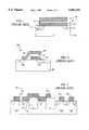
- FIG. 1illustrates a non-volatile memory device 10a, shown as a flash EPROM device.
- Memory 10ais illustrative of a single transistor memory cell typically connected within an array of cells formed on a semiconductor substrate.
- Device 10ais shown having a drain 12 and a double-diffused source 14 formed within a p-type substrate 16.
- Device 10ais programmed by drawing electrons from drain 12, through tunnel oxide 18 and into floating gate 20.
- Tunnel oxide 18is relatively thin to allow traverse of hot electrons during the program or erase cycle.
- source 14is connected common throughout the array.
- a dielectric 22is shown interposed between floating gate 20 and a control gate 24, wherein control gate 24 is generally connected to a word line and drain 12 is generally connected to a bit line.
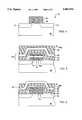
- Device 10bincludes source and drain regions 26 and 28 provided within substrate 30. Tunnel oxide layer 32 is provided on the surface of substrate 30 under a floating gate 34. Floating gate 34 overlaps a portion of drain 28 and a portion of a channel formed between source 26 and drain 28. A dielectric 36 separates floating gate 34 from control gate 38.
- the device structure 10bfunctions as a two transistor set; one transistor is the floating gate memory transistor and the other transistor is a series-connected enhancement transistor controlled by control gate 38.
- Single cell memory devices 10a and 10bare but two exemplary forms of a non-volatile memory cell. There are numerous other forms used for storing electrons programmed upon a floating gate.
- FIG. 3illustrates yet another exemplary form. Instead of stacking a control gate upon a floating gate, FIG. 3 illustrates a memory device or cell 10c having non-stacked floating and control gates. Specifically, FIG. 3 illustrates a single cell memory device 10c having a floating gate 40 laterally displaced from control gate 42. Memory device 10c thereby indicates a single memory cell having three transistors: a program transistor Q1, a sense transistor Q2 and a read transistor Q3. A tunnel oxide 44 is formed between floating gate 40 and a drain side 43 of program transistor Q1.
- Electronsare thereby injected onto floating gate 40 by activation of program transistor Q1.
- Floating gate 40can therefore be programmed with injected electrons which control activation of sense transistor Q2 in accordance with the quantity of electrons injected upon the floating gate 40.
- the conventional forms shown in FIGS. 1-3are each illustrative of a floating gate 20, 34 and 40.
- a respective control gate 24, 38 and 42may or may not cause turn-on of the transistor associated with the floating gate depending upon whether the floating gate is programmed or not.
- the present processis presented to form a non-volatile memory device or cell which is less susceptible to the charge loss phenomena.
- the process hereofis designed to make less available positively charged atoms within the dielectric structures which surround a floating gate.
- Each dielectric which resides above and about a floating gate, or above and about a stacked pair of floating and control gates,is carefully processed such that positively charged atoms are not formed within those dielectrics either during the fabrication process or after fabrication is complete and the device is field operable.
- elemental hydrogen present in the structure of certain dielectricsis the primary source of positively charged atoms within a non-volatile memory device topography.
- the hydrogen atomsarise from the chemical composition of hydrogen-bearing dielectric layers residing above or around the floating gate.
- the present applicantsdetermined that the hydrogen atoms are released from their bonding sites whenever they are subjected to temperatures exceeding a critical level. For that reason, the present fabrication process is designed to reduce the disruption of hydrogen from its bond site and thereby reduce the availability of positively charged hydrogen atoms within the overlying dielectric layers.
- the availability of positively charged hydrogen atomsare minimized by (i) reducing temperatures used in the formation of hydrogen-containing dielectrics, (ii) reducing temperatures used in the formation of dielectrics and conductors subsequent to the deposition of hydrogen-containing dielectrics and (iii) reducing post dielectric/conductor formation temperatures (i.e., reducing sintering, alloying and annealing temperatures) .
- reducing temperatures used in the formation of hydrogen-containing dielectricsreducing temperatures used in the formation of dielectrics and conductors subsequent to the deposition of hydrogen-containing dielectrics and (iii) reducing post dielectric/conductor formation temperatures (i.e., reducing sintering, alloying and annealing temperatures) .
- the critical temperature over which predominant amounts of positively charged hydrogen atoms appearis approximately 380° C.
- hydrogen-containing dielectrics as well as subsequent dielectrics/conductorsare formed at temperatures less than 380° C. in most instances and less than 350° C. in other instances
- the various layers overlying the floating gatedo not produce substantial amounts of positively charged, free atomic hydrogen. Absent large amounts of atomic hydrogen residing within the overlying dielectric regions, lesser amounts of positively charged source atoms are present which can deleteriously neutralize a programmed, negatively charged floating gate. That is, reduction in the availability of positively charged atomic hydrogen is experimentally shown to equate with a reduction in problems associated with the charge loss phenomenon.
- the hydrogenis typically bonded within, for example, a Si--H, N--H and/or Si--OH structure within one or more dielectrics overlying the floating gate.
- the dielectricsreside directly on top of or a spaced distance above a floating gate.
- the floating gatecan be configured absent a control gate stacked thereover, or the floating gate can be formed as a lower conductor spaced below a control gate. In the latter instance, the dielectrics are generally formed above both the floating gate as well as the control gate. In either instance, the dielectrics are formed using fabrication techniques of chemical vapor deposition (CVD) or spin-on techniques.
- CVDchemical vapor deposition
- CVD and spin-on application of dielectricsoften utilize a hydrogen base material or carrier material which bonds within the resulting dielectric layer or layers. It is postulated that the Si--H bonds are broken at lower temperatures than the N--H bonds or the Si--OH bonds. It is therefore desirable that whatever bonds are formed in the dielectric, those bonds be strong bonds and not easily broken. Preferably, a prevalent amount of those bonds should be N--H or Si--OH bonds rather than Si--H bonds.
- hydrogenis used in forming a passivation layer typically located at the uppermost layer of the semiconductor topography.
- Hydrogenis also present in the spin-on dielectric materials located between the floating (or control gate) and the passivation layer.
- a popular spin-on dielectric materialcomprises siloxanes or silicates mixed in an alcohol-based solvent. Hydrogen sourced from the oxynitride passivation layer or the SOG layer can cause deleterious charge loss upon a programmed floating gate absent low temperature processing of the present invention. By minimizing the temperature at which passivation and SOG layers are formed, or any hydrogen-containing dielectric is formed, positively charged atoms are made less available for migration to and neutralization of electrons upon a programmed floating gate.
- the present inventioncontemplates a method for fabricating a non-volatile PROM memory device.
- the methodcomprises the steps of growing a tunnel oxide upon a semiconductor substrate. Thereafter, a floating gate (floating conductor) is patterned upon the tunnel oxide. A temperature less than 380° C. is then used to form, at an elevational level above the floating conductor, a hydrogen-containing dielectric layer. Thereafter, a combination of dielectric and conductive layers are formed at temperatures less than 380° C. upon the hydrogen-containing dielectric layer.
- the hydrogen-containing dielectric layeris either deposited upon a floating conductor or is deposited a spaced distance above the floating conductor.
- control conductorincludes a conductor insulatively spaced above or laterally from the floating conductor.
- control conductor and floating conductorare each made of polycrystalline silicon or polysilicon.
- the present inventionfurther contemplates a method for fabricating a memory device having a floating gate.
- the methodincludes the steps of providing a semiconductor substrate upon which a tunnel oxide is formed. Thereafter, a floating gate is deposited upon the tunnel oxide and an intermediate oxide is formed upon the floating gate. A control gate is thereafter deposited upon the intermediate oxide and, at an elevation level above the control gate, a hydrogen-containing dielectric is deposited.
- the hydrogen-containing dielectricincludes bonded hydrogen which remains in its bonded location during formation of the dielectric. Moreover, the hydrogen remains bonded during times in which the previously formed dielectric is exposed to heat cycles--i.e., metal alloy/sintering heat cycles, etc.
- the present inventioncontemplates a method for fabricating a memory device having a floating gate.
- the methodincludes the steps of providing a semiconductor substrate upon which a tunnel oxide is formed.
- a floating gateis thereafter deposited upon the tunnel oxide and, at an elevation level above the floating gate, a hydrogen-containing dielectric is deposited.
- the hydrogen-containing dielectricincludes bonded hydrogen which remains in its bonded location during formation of the dielectric and during times in which the dielectric is exposed to heat cycles which occur after dielectric fabrication.
- the heat cyclesinclude fabrication heat cycles, metal alloy heat cycles or heat cycles associated with memory device operation in the field.
- the present inventionfurther contemplates a non-volatile memory cell.
- the memory cellincludes a semiconductor substrate containing impurity implant regions and a tunnel oxide placed upon the substrate.
- a polysilicon stripis placed upon the tunnel oxide.
- the polysilicon stripis adapted to receive electrons injected from one of the impurity implant regions during the program cycle of the memory cell.
- a dielectric comprising hydrogenis formed above the polysilicon strip. The dielectric is formed at a temperature less than 380° C. to minimize formation and movement of free atomic hydrogen from the dielectric to the electrons injected upon the polysilicon strip. It is contemplated that hydrogen remains in its bonded location when the hydrogen-containing dielectric is exposed to ambient temperatures less than 400° C.
- FIG. 1is a partial, cross-sectional view of a conventional memory cell having a stacked pair of floating and control conductors
- FIG. 2is a partial, cross-sectional view of another conventional memory cell having partially overlapping floating and control conductors coupled to form a series--connected pair of transistors;
- FIG. 3is a partial, cross-sectional view of yet another conventional memory cell having a single level floating conductor laterally spaced from a control conductor;
- FIG. 4is a partial, cross-sectional view of a memory cell formed at an early stage of fabrication according to the present invention.
- FIGS. 5-7are partial, cross-sectional views of the memory cell of FIG. 4 formed at successive stages of fabrication according to the present invention.
- FIG. 8is a schematic of a circuit used to test the charge retention (or charge loss) of a programmed floating gate
- FIG. 9is a graph of experimental results depicting failure rate derived from the test circuit of FIG. 8 and taken as a function of dielectric/conductor processing temperatures;
- FIG. 10is a graph of pre- and post-bake failure rates derived from the test circuit of FIG. 8 and taken as a function of dielectric/conductor processing temperatures;
- FIGS. 11 and 12are partial, cross-sectional views of memory cells having one or more metallization levels (conductors) deposited at an elevational level above a floating gate according to the present invention.
- FIG. 4illustrates a single cell, non-volatile PROM memory device 50 formed at an early stage of development.
- Memory device 50includes source and drain regions 52 and 54 placed within a semiconductor substrate 56.
- Substrate 56is a p-type single crystal silicon substrate, wherein source and drain regions 52 and 54, respectively, are of n-type impurity.
- Memory device 50includes any memory configuration having a floating gate insulatively spaced upon the upper surface of substrate 56.
- memory device 50includes an EEPROM, an EPROM and/or a flash EPROM.
- oxide 58grown upon the upper surface of substrate 56 is a thin oxide 58, generally less than 100 Angstroms thick. At least a portion of oxide 58 comprises a tunnel region through which electrons can tunnel to and from an overlying floating conductor 60.
- Floating conductor 60is made of polysilicon. Oxide 58 is SiO 2 thermally grown in an oxygen-containing dry ambient. It is understood that floating conductor 60 can be the lower conductor in a stacked pair of floating and control conductors. Alternatively, floating conductor 60 can be configured in a non-stacked arrangement, wherein floating conductor 60 is laterally spaced from a control conductor. It is further understood that in either arrangement (stacked or non-stacked) at least one dielectric layer is formed above floating conductor 60. Thus, FIG. 4 illustrates a generic floating conductor upon which a control conductor can be formed above or laterally spaced therefrom.
- FIG. 5is presented to clarify the various configurations of floating conductor 60, shown in FIG. 4, FIG. 5 illustrates floating conductor 60b represented in a non-stacked configuration absent an overlying control conductor.
- floating conductor 60acan be represented in a stacked configuration with control conductor 61 insulatively spaced thereover. It is understood that, in a stacked configuration, floating conductor 60a illustrated in FIG. 5 can be the lower conductor 60a of a stacked arrangement of floating conductor 60a and control conductor 61.
- floating conductor 60bcomprises the entire conductive element (absent an intervening oxide spacer 63).
- a series of dielectric layers 62, 64, 66, 68are configured upon the conductor elements.
- Each dielectric layerconsists of a material which permits the passage of electromagnetic field but does not conduct a substantial amount of current.
- Layer 62can suitably be formed as an oxide within a CVD chamber.
- Layer 62can be formed either in atmospheric or low pressure conditions (i.e., as an APCVD or LPCVD oxide).
- Layer 64is suitably formed as a borophosphosilicate glass (BPSG).
- BPSGis preferably formed in an LPCVD chamber and reflowed in a nitrogen (N 2 ) ambient or oxygen (O 2 ) ambient instead of a hydrogen-bearing steam ambient.
- Reflowoccurs at a temperature between 700° C. and 900° C. Reflow allows a gradual contour at locations 65.
- One advantage of reflowis improved step coverage for subsequently placed dielectrics/conductors.
- Layer 66is suitably formed within a plasma enhanced CVD chamber (PECVD chamber). RF-induced glow discharge transfers energy into the silicon-based reactant gasses, thereby allowing substrate 56 to remain at a lower temperature than in counterpart APCVD or LPCVD processes. PECVD can be carried forth using, for example, parallel plate reactors or horizontal tube reactors.
- Layer 68is suitably formed as a spin-on glass (SOG). SOG is preferably formed from a siloxane-based material and is applied in liquid form. After application, SOG is cured to exhibit planarization capabilities similar to those of polyimide films. SOG is chosen to fill voids or valleys thereby leaving a substantially planar upper surface 69a.
- FIG. 6upper surface 69a (shown in FIG. 5) in a step subsequent to that of FIG. 5.
- a portion of SOG 68is sacrificially etched back to present an exposed upper surface region of dielectric layer 66 substantially coplanar with exposed upper surface 69b of SOG 68.
- dielectric 68remains only in the troughs or valleys between raised regions of layer 66.
- FIG. 7a pair of dielectrics 70 and 72 are deposited upon the exposed upper surface of dielectrics 68 and 66 in a step subsequent to that shown in FIG. 6.
- FIG. 7illustrates dielectric layer 70 formed upon layers 68 and 66, and dielectric layer 72 formed upon dielectric layer 70.
- Dielectric layer 70is suitably formed as an oxide within a PECVD system under conditions similar to that used in forming the PECVD layer 66.
- SOG layer 68is sandwiched between PECVD layer 66 and PECVD layer 70.
- Layer 72is suitably formed as a dielectric layer which passivates the underlying semiconductor wafer topography.
- layer 72is the final layer deposited upon a semiconductor layer.
- Layer 72includes a passivation material chosen to present a barrier against moisture and sodium ingress from the outside environment to underlying wafer topography. Suitable passivation material includes nitride or oxynitride material. After passivation layer 72 is formed, windows are etched through the passivation layer in the regions overlying die bonding pads (not shown).
- Substantial amounts of hydrogenare generally present when SOGs, nitrides or oxynitrides are formed.
- hydrogenoccurs in the formation of the exemplary structure set forth in FIG. 7, at layers 68 and 72. If not inhibited, the hydrogen in those layers can break from their bond locations and migrate as positively charged atoms to floating conductor 60 operatively programmed with a negative potential. Measures must therefore be taken to prevent origination of hydrogen atoms from the bond locations and migration of those hydrogen atoms to negatively charged (programmed) floating gate 60.
- any dielectric or conductive layer having hydrogen as a constituent in its formationis hereby formed at temperatures less than 380° C. and in some instances less than 350° C .
- any layer (either a layer having a hydrogen constituent or one not having a hydrogen constituent) formed after the initial hydrogen-containing layeris hereby formed at a temperature less than 380° C. Accordingly, low temperature formation of critical layers is thereby used to ensure minimal disruption of certain types of hydrogen bonds within the hydrogen-bearing layers.
- FIG. 7illustrates a dual level metallization scheme, wherein metallization layers (not shown in FIG. 7 but shown in FIG. 11) are formed at several levels between the floating gate and the passivation layer.
- FIGS. 11 and 12 described herein beloware further illustrative of distinctions between a single level and a dual level metallization scheme, wherein metallization is shown.
- FIGS. 4-7do not illustrate the metallization levels for sake of clarity and brevity.
- the charge lossis experimentally discovered as being caused primarily by the diffusion of hydrogen atoms from a hydrogen-containing source layer, such as the oxynitride passivation layer 72 and/or SOG layer 68 to a negatively charged floating gate 60. Dielectric layers 72 and 68 thereby appear as containing hydrogen.
- the hydrogen atoms(positively charged atoms) gain freedom during high temperature fabrication from a bond location within the dielectric layer and travel during operation of the memory device to a "programmed" negatively charged floating gate. Accumulation of positively charged hydrogen atoms upon the negatively charged floating gate neutralizes the programmed voltage upon the floating gate.
- a result of neutralization (or negative charge loss)is the deleterious deletion of information stored within the supposedly non-volatile PROM device.
- C(x,t)represents the hydrogen concentration which is proportional to the distance x traveled by the hydrogen atoms from the dielectric source to the underlying floating gate 60.
- Time trepresents the time it takes for the hydrogen atoms to travel to floating gate 60.
- C 0is the concentration of hydrogen within the various dielectric layers; erfc is the complementary error function; and, D is the diffusion coefficient of hydrogen in the medium (intermediate dielectric layers) through which it travels.
- the diffusion coefficient D of hydrogendepends upon temperature, as shown below: ##EQU2## , wherein E a is the activation energy, k is the Boltzman constant, and T is the temperature in Kevlin.
- E ais the activation energy
- kis the Boltzman constant
- Tis the temperature in Kevlin.
- hydrogen within the hydrogen-containing dielectricsexists in several different forms depending upon the deposition conditions of the hydrogen-containing layers.
- hydrogencan be bonded within the hydrogen-containing layers as Si--H, N--H and/or Si--OH.
- the Si--H bondis broken at a temperature of approximately 250° C. or more.
- the N--H bondis broken at a temperature of about 400° C. or more.
- the Si--OH bondis broken at a temperature of approximately 700° C. or more.
- the number of hydrogen atoms available for diffusiondepends upon the temperature at which the hydrogen-containing dielectric layer are formed. Formation of the hydrogen-containing layers must therefore be controlled at temperatures less than 380° C., and in some instances less than 350° C.
- the alloy or sintering steps used to form the metal-silicon interfacemust therefore be performed at temperatures less than 380° C. for all metallization formed after the deposition of the first hydrogen-containing dielectric layer (provided the hydrogen-containing layer is formed after, and spaced upon or above floating conductor 60).
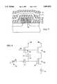
- FIG. 8illustrates a circuit schematic used to test charge retention capability of a floating gate. Specifically, FIG. 8 illustrates a circuit schematic representative of the cross-sectional topography shown in FIG. 3.
- a positive charge from a variable voltage source 80is applied to capacitor C1.
- On the opposing plate of capacitor C1is a corresponding negative charge buildup.
- the negative charge on capacitor C1draws a positive charge upon floating gate 82 of sense transistor Q2.
- An increase in voltage supply 80corresponds with an increase in positive charge upon the floating gate thereby causing charge loss or charge neutralization of a floating gate 82.
- a natural result of charge neutralizationis an increase in current read at ammeter 84.
- FIG. 8illustrates an exemplary cell of a memory device. There may be numerous other configurations of a memory cell, each configuration can be measured for the quantity of electron charge loss at the floating gate resulting from voltage supplied thereto.
- an increase in voltage value by source 80causes at corresponding decrease in electrons upon floating gate 82.
- the decrease in electronsis read by meter 84.
- Voltage source 80is applied via overlying dielectric layers (represented as capacitor C1) to the floating gate polysilicon (floating gate 60 of the structure shown in FIG. 7) to provide relative charge retention data associated with atomic hydrogen which might be available as a result of processing within dielectric layers overlying floating gate 60.
- the actual experimental results of voltage source and corresponding current readings taken from a memory device, such one formed by the process presented in reference to FIGS. 4-7,is depicted in FIGS. 9 and 10.
- FIG. 9illustrates nine groups of wafers 90-106. Each group is processed according to a different dielectric deposition temperature and metal alloy temperature.
- the groups of waferscontain hydrogen-bearing dielectrics deposited at one of three deposition temperatures ("dep temp" of 350° C., 400° C. and 430° ), and also contain metallization layers alloyed at one of three alloy temperatures ("alloy temp" of 350° C., 370° C. and 390° ).
- FIG. 9thereby illustrates nine separate and unique deposition/alloy temperatures.
- a first group 90contains dielectrics formed at 350° C. and metal alloyed at 350° C.
- a next group 92contains dielectrics deposited at 350° C.
- a third group 94contains dielectrics deposited at 350° C. and metal alloyed at 390° C.
- a fourth group 96contains dielectrics deposited at 400° C. and metal alloyed at 350° C. Changes to deposition temperature and metal alloy temperature are continued for each group, through wafer group 106.
- FIG. 9illustrates wafer grouping 106 having an average failure of approximately 420 die per wafer. Die failure is deemed as a single cell operates outside a pre-determined margin, referred to in FIG. 9 as a "margin loss” criteria.
- "margin loss”refers to a predetermined amount of charge loss upon the floating gate as a relative proportion to the original charge thereon. Margin loss thereby represents a loss in charge as measured by meter 84 in FIG. 8 caused by a corresponding increase in voltage source 80. For example, a pre-determined margin might be 20 percent.
- FIG. 9illustrates a preponderance of failed die, approximately 420, whenever the hydrogen-bearing dielectric, and subsequent dielectrics are formed at fabrication temperatures approximating 430° C.
- FIG. 10illustrates a first wafer sort (WS1) and a second wafer sort (WS2), wherein the defective die discovered within the second wafer sort is taken relative to defective die within the first wafer sort.
- Wafer sortis defined herein as the test procedure in which die are tested according to the test circuit set forth in FIG. 8, and die are deemed "failed" upon detection of charge loss outside a pre-determined margin set forth above. Similar to the test procedure used in FIG. 9, FIG.
- testingis begun at a first wafer sort operation, after the memory cell array is fabricated and floating gates are programmed. Testing is performed using the device of FIG. 8 to present a margin loss at the first wafer sort step. Thereafter, the wafer is heated, or "baked" at a temperature of approximately 250° C., and another wafer sort (WS2) operation is undertaken. Using the first wafer sort set at a benchmark of 100 percent good die, a second wafer sort is shown in FIG. 10 relative to the first wafer sort. Thus, wafer grouping 124 illustrates approximately 16 die which failed the second wafer sort and which did not fail the first wafer sort.
- WS2wafer sort
- FIGS. 11 and 12partial, cross-sectional views of a memory cell 100 and 102, respectively are shown.
- Memory cell 100includes a single level of metallization 104.
- FIG. 12illustrates two metallization levels 106 and 108.
- Device 102is shown having a plurality of dielectrics, including floating conductor 60 similar to the configuration of FIG. 7.
- FIG. 12is presented to illustrate metallization layers interspersed between the dielectric layers, as the dielectric layers are formed upon floating conductor 60.
- the metallization layerscan extend over floating conductor 60, but are shown in FIG. 12 laterally spaced from floating conductor 60.
- FIG. 11illustrates a single level of metallization 104 interspersed between dielectrics. The dielectrics in FIG.
- FIG. 11illustrates a non-sacrificial SOG layer 110 sandwiched between a pair of oxynitride layers 112 and 114.
- dielectric layerscan be arranged in any workable configuration and, regardless of that configuration, metallization layers (one or more), can be formed between pairs of those dielectrics.
- alloy and sintering of metal conductive layersmust also be controlled so as to achieve an optimal, overall processing temperature.
Landscapes
- Physics & Mathematics (AREA)
- Condensed Matter Physics & Semiconductors (AREA)
- General Physics & Mathematics (AREA)
- Engineering & Computer Science (AREA)
- Computer Hardware Design (AREA)
- Microelectronics & Electronic Packaging (AREA)
- Power Engineering (AREA)
- Non-Volatile Memory (AREA)
- Semiconductor Memories (AREA)
- Formation Of Insulating Films (AREA)
Abstract
Description
Claims (27)
Priority Applications (7)
| Application Number | Priority Date | Filing Date | Title |
|---|---|---|---|
| US08/393,138US5801076A (en) | 1995-02-21 | 1995-02-21 | Method of making non-volatile memory device having a floating gate with enhanced charge retention |
| EP96300640AEP0729187B1 (en) | 1995-02-21 | 1996-01-30 | Non-volatile semiconductor memory device and method of manufacturing the same |
| AT96300640TATE215736T1 (en) | 1995-02-21 | 1996-01-30 | NON-VOLATILE SEMICONDUCTOR MEMORY ARRANGEMENT AND PRODUCTION METHOD |
| DE69620283TDE69620283T2 (en) | 1995-02-21 | 1996-01-30 | Non-volatile semiconductor memory device and manufacturing method |
| KR1019960003601AKR100431551B1 (en) | 1995-02-21 | 1996-02-14 | Method for fabricating nonvolatile memory device having floating gate with improved charge retention performance |
| JP03182996AJP4458498B2 (en) | 1995-02-21 | 1996-02-20 | Method and non-volatile memory cell for fabricating a non-volatile memory device |
| US08/815,835US5805013A (en) | 1995-02-21 | 1997-03-12 | Non-volatile memory device having a floating gate with enhanced charge retention |
Applications Claiming Priority (1)
| Application Number | Priority Date | Filing Date | Title |
|---|---|---|---|
| US08/393,138US5801076A (en) | 1995-02-21 | 1995-02-21 | Method of making non-volatile memory device having a floating gate with enhanced charge retention |
Related Child Applications (1)
| Application Number | Title | Priority Date | Filing Date |
|---|---|---|---|
| US08/815,835DivisionUS5805013A (en) | 1995-02-21 | 1997-03-12 | Non-volatile memory device having a floating gate with enhanced charge retention |
Publications (1)
| Publication Number | Publication Date |
|---|---|
| US5801076Atrue US5801076A (en) | 1998-09-01 |
Family
ID=23553433
Family Applications (2)
| Application Number | Title | Priority Date | Filing Date |
|---|---|---|---|
| US08/393,138Expired - LifetimeUS5801076A (en) | 1995-02-21 | 1995-02-21 | Method of making non-volatile memory device having a floating gate with enhanced charge retention |
| US08/815,835Expired - LifetimeUS5805013A (en) | 1995-02-21 | 1997-03-12 | Non-volatile memory device having a floating gate with enhanced charge retention |
Family Applications After (1)
| Application Number | Title | Priority Date | Filing Date |
|---|---|---|---|
| US08/815,835Expired - LifetimeUS5805013A (en) | 1995-02-21 | 1997-03-12 | Non-volatile memory device having a floating gate with enhanced charge retention |
Country Status (6)
| Country | Link |
|---|---|
| US (2) | US5801076A (en) |
| EP (1) | EP0729187B1 (en) |
| JP (1) | JP4458498B2 (en) |
| KR (1) | KR100431551B1 (en) |
| AT (1) | ATE215736T1 (en) |
| DE (1) | DE69620283T2 (en) |
Cited By (49)
| Publication number | Priority date | Publication date | Assignee | Title |
|---|---|---|---|---|
| US6133095A (en)* | 1999-02-04 | 2000-10-17 | Saifun Semiconductors Ltd. | Method for creating diffusion areas for sources and drains without an etch step |
| US6204125B1 (en) | 1999-06-28 | 2001-03-20 | Hyundai Electronics Industries Co., Ltd. | Method of forming a gate in a stack gate flash EEPROM cell |
| US6274395B1 (en)* | 1999-12-23 | 2001-08-14 | Lsi Logic Corporation | Method and apparatus for maintaining test data during fabrication of a semiconductor wafer |
| US6284602B1 (en) | 1999-09-20 | 2001-09-04 | Advanced Micro Devices, Inc. | Process to reduce post cycling program VT dispersion for NAND flash memory devices |
| US6303440B1 (en)* | 1995-10-02 | 2001-10-16 | Kabushiki Kaisha Toshiba | Nonvolatile semiconductor memory, and method of manufacturing the same |
| US6319847B1 (en)* | 1997-03-31 | 2001-11-20 | Nec Corporation | Semiconductor device using a thermal treatment of the device in a pressurized steam ambient as a planarization technique |
| US6429063B1 (en) | 1999-10-26 | 2002-08-06 | Saifun Semiconductors Ltd. | NROM cell with generally decoupled primary and secondary injection |
| US6444521B1 (en)* | 2000-11-09 | 2002-09-03 | Macronix International Co., Ltd. | Method to improve nitride floating gate charge trapping for NROM flash memory device |
| US6490204B2 (en) | 2000-05-04 | 2002-12-03 | Saifun Semiconductors Ltd. | Programming and erasing methods for a reference cell of an NROM array |
| US6538270B1 (en)* | 2000-05-16 | 2003-03-25 | Advanced Micro Devices, Inc. | Staggered bitline strapping of a non-volatile memory cell |
| US6552387B1 (en) | 1997-07-30 | 2003-04-22 | Saifun Semiconductors Ltd. | Non-volatile electrically erasable and programmable semiconductor memory cell utilizing asymmetrical charge trapping |
| US20030096476A1 (en)* | 2001-11-19 | 2003-05-22 | Ilan Bloom | Protective layer in memory device and method therefor |
| US6583007B1 (en) | 2001-12-20 | 2003-06-24 | Saifun Semiconductors Ltd. | Reducing secondary injection effects |
| US6584017B2 (en) | 2001-04-05 | 2003-06-24 | Saifun Semiconductors Ltd. | Method for programming a reference cell |
| US6649972B2 (en) | 1997-08-01 | 2003-11-18 | Saifun Semiconductors Ltd. | Two bit non-volatile electrically erasable and programmable semiconductor memory cell utilizing asymmetrical charge trapping |
| US6664588B2 (en) | 1998-05-20 | 2003-12-16 | Saifun Semiconductors Ltd. | NROM cell with self-aligned programming and erasure areas |
| US6788574B1 (en) | 2001-12-06 | 2004-09-07 | Virage Logic Corporation | Electrically-alterable non-volatile memory cell |
| US6826107B2 (en) | 2002-08-01 | 2004-11-30 | Saifun Semiconductors Ltd. | High voltage insertion in flash memory cards |
| US6829172B2 (en) | 2000-05-04 | 2004-12-07 | Saifun Semiconductors Ltd. | Programming of nonvolatile memory cells |
| US6842375B1 (en) | 2001-12-06 | 2005-01-11 | Virage Logic Corporation | Methods and apparatuses for maintaining information stored in a non-volatile memory cell |
| US6850446B1 (en) | 2001-12-06 | 2005-02-01 | Virage Logic Corporation | Memory cell sensing with low noise generation |
| US6928001B2 (en) | 2000-12-07 | 2005-08-09 | Saifun Semiconductors Ltd. | Programming and erasing methods for a non-volatile memory cell |
| US6992938B1 (en) | 2001-12-06 | 2006-01-31 | Virage Logic Corporation | Methods and apparatuses for test circuitry for a dual-polarity non-volatile memory cell |
| US20060208281A1 (en)* | 2005-03-17 | 2006-09-21 | Saifun Semiconductors, Ltd. | Contact in planar NROM technology |
| US7130213B1 (en) | 2001-12-06 | 2006-10-31 | Virage Logic Corporation | Methods and apparatuses for a dual-polarity non-volatile memory cell |
| US20060292842A1 (en)* | 1998-10-13 | 2006-12-28 | Stmicroelectronics, Inc. | Self-aligned gate and method |
| US20070069714A1 (en)* | 2005-09-27 | 2007-03-29 | Saifun Semiconductors, Ltd. | Method for measuring charge pump output current |
| US20070200180A1 (en)* | 2006-02-28 | 2007-08-30 | Rustom Irani | Double density NROM with nitride strips (DDNS) |
| US7317633B2 (en) | 2004-07-06 | 2008-01-08 | Saifun Semiconductors Ltd | Protection of NROM devices from charge damage |
| US7352627B2 (en) | 2006-01-03 | 2008-04-01 | Saifon Semiconductors Ltd. | Method, system, and circuit for operating a non-volatile memory array |
| US7369440B2 (en) | 2005-01-19 | 2008-05-06 | Saifun Semiconductors Ltd. | Method, circuit and systems for erasing one or more non-volatile memory cells |
| US7420848B2 (en) | 2002-01-31 | 2008-09-02 | Saifun Semiconductors Ltd. | Method, system, and circuit for operating a non-volatile memory array |
| US7457183B2 (en) | 2003-09-16 | 2008-11-25 | Saifun Semiconductors Ltd. | Operating array cells with matched reference cells |
| US7466594B2 (en) | 2004-08-12 | 2008-12-16 | Saifun Semiconductors Ltd. | Dynamic matching of signal path and reference path for sensing |
| US7518908B2 (en) | 2001-01-18 | 2009-04-14 | Saifun Semiconductors Ltd. | EEPROM array and method for operation thereof |
| US7532529B2 (en) | 2004-03-29 | 2009-05-12 | Saifun Semiconductors Ltd. | Apparatus and methods for multi-level sensing in a memory array |
| US7535765B2 (en) | 2004-12-09 | 2009-05-19 | Saifun Semiconductors Ltd. | Non-volatile memory device and method for reading cells |
| US7605579B2 (en) | 2006-09-18 | 2009-10-20 | Saifun Semiconductors Ltd. | Measuring and controlling current consumption and output current of charge pumps |
| US7638850B2 (en) | 2004-10-14 | 2009-12-29 | Saifun Semiconductors Ltd. | Non-volatile memory structure and method of fabrication |
| US7668017B2 (en) | 2005-08-17 | 2010-02-23 | Saifun Semiconductors Ltd. | Method of erasing non-volatile memory cells |
| US7675782B2 (en) | 2002-10-29 | 2010-03-09 | Saifun Semiconductors Ltd. | Method, system and circuit for programming a non-volatile memory array |
| US7692961B2 (en) | 2006-02-21 | 2010-04-06 | Saifun Semiconductors Ltd. | Method, circuit and device for disturb-control of programming nonvolatile memory cells by hot-hole injection (HHI) and by channel hot-electron (CHE) injection |
| US7701779B2 (en) | 2006-04-27 | 2010-04-20 | Sajfun Semiconductors Ltd. | Method for programming a reference cell |
| US7738304B2 (en) | 2002-07-10 | 2010-06-15 | Saifun Semiconductors Ltd. | Multiple use memory chip |
| US7743230B2 (en) | 2003-01-31 | 2010-06-22 | Saifun Semiconductors Ltd. | Memory array programming circuit and a method for using the circuit |
| US7760554B2 (en) | 2006-02-21 | 2010-07-20 | Saifun Semiconductors Ltd. | NROM non-volatile memory and mode of operation |
| US7786512B2 (en) | 2005-07-18 | 2010-08-31 | Saifun Semiconductors Ltd. | Dense non-volatile memory array and method of fabrication |
| US7808818B2 (en) | 2006-01-12 | 2010-10-05 | Saifun Semiconductors Ltd. | Secondary injection for NROM |
| US8253452B2 (en) | 2006-02-21 | 2012-08-28 | Spansion Israel Ltd | Circuit and method for powering up an integrated circuit and an integrated circuit utilizing same |
Families Citing this family (7)
| Publication number | Priority date | Publication date | Assignee | Title |
|---|---|---|---|---|
| US5940735A (en)* | 1997-08-25 | 1999-08-17 | Advanced Micro Devices, Inc. | Reduction of charge loss in nonvolatile memory cells by phosphorus implantation into PECVD nitride/oxynitride films |
| US6720861B1 (en)* | 1999-03-12 | 2004-04-13 | Best Access Systems | Wireless security control system |
| KR100546392B1 (en)* | 2003-11-01 | 2006-01-26 | 삼성전자주식회사 | Semiconductor device including EPROM element and manufacturing method thereof |
| US20060237802A1 (en)* | 2005-04-21 | 2006-10-26 | Macronix International Co., Ltd. | Method for improving SOG process |
| US20060292774A1 (en)* | 2005-06-27 | 2006-12-28 | Macronix International Co., Ltd. | Method for preventing metal line bridging in a semiconductor device |
| JP4826724B2 (en)* | 2005-08-25 | 2011-11-30 | セイコーエプソン株式会社 | Trimming switch |
| KR102567236B1 (en)* | 2022-02-09 | 2023-08-16 | 연세대학교 산학협력단 | 2-terminal memory device and manufacturing method thereof |
Citations (27)
| Publication number | Priority date | Publication date | Assignee | Title |
|---|---|---|---|---|
| US4422161A (en)* | 1981-10-08 | 1983-12-20 | Rca Corporation | Memory array with redundant elements |
| US4581622A (en)* | 1979-09-14 | 1986-04-08 | Fujitsu Limited | UV erasable EPROM with UV transparent silicon oxynitride coating |
| EP0196806A1 (en)* | 1985-03-11 | 1986-10-08 | Applied Materials, Inc. | Optimized process for forming borophosphosilicate glass |
| US4958321A (en)* | 1988-09-22 | 1990-09-18 | Advanced Micro Devices, Inc. | One transistor flash EPROM cell |
| EP0409107A2 (en)* | 1989-07-18 | 1991-01-23 | Sony Corporation | A nonvolatile semiconductor memory device and a method of manufacturing thereof |
| US4999812A (en)* | 1988-11-23 | 1991-03-12 | National Semiconductor Corp. | Architecture for a flash erase EEPROM memory |
| US5070032A (en)* | 1989-03-15 | 1991-12-03 | Sundisk Corporation | Method of making dense flash eeprom semiconductor memory structures |
| EP0461764A2 (en)* | 1990-06-13 | 1991-12-18 | WaferScale Integration Inc. | EPROM virtual ground array |
| US5077691A (en)* | 1989-10-23 | 1991-12-31 | Advanced Micro Devices, Inc. | Flash EEPROM array with negative gate voltage erase operation |
| EP0464432A2 (en)* | 1990-06-29 | 1992-01-08 | National Semiconductor Corporation | Asymmetrical virtual ground EPROM cell & fabrication method |
| US5101250A (en)* | 1988-06-28 | 1992-03-31 | Mitsubishi Denki Kabushiki Kaisha | Electrically programmable non-volatile memory device and manufacturing method thereof |
| US5120672A (en)* | 1989-02-22 | 1992-06-09 | Texas Instruments Incorporated | Fabricating a single level merged EEPROM cell having an ONO memory stack substantially spaced from the source region |
| US5120671A (en)* | 1990-11-29 | 1992-06-09 | Intel Corporation | Process for self aligning a source region with a field oxide region and a polysilicon gate |
| EP0498604A1 (en)* | 1991-02-04 | 1992-08-12 | Motorola, Inc. | Semiconductor device having a teos based spin-on-glass and process for making the same |
| US5147811A (en)* | 1990-03-13 | 1992-09-15 | Kabushiki Kaisha Toshiba | Method of manufacturing semiconductor device by controlling the profile of the density of p-type impurities in the source/drain regions |
| US5149666A (en)* | 1987-01-07 | 1992-09-22 | Kabushiki Kaisha Toshiba | Method of manufacturing a semiconductor memory device having a floating gate electrode composed of 2-10 silicon grains |
| US5151375A (en)* | 1990-06-13 | 1992-09-29 | Waferscale Integration, Inc. | EPROM virtual ground array |
| US5208175A (en)* | 1990-12-21 | 1993-05-04 | Samsung Electronics Co., Ltd. | Method of making a nonvolatile semiconductor memory device |
| EP0552531A1 (en)* | 1992-01-22 | 1993-07-28 | Macronix International Co., Ltd. | Non-volatile memory cell and array architecture |
| EP0573169A1 (en)* | 1992-06-02 | 1993-12-08 | National Semiconductor Corporation | Segment-erasable flash EPROM |
| US5279981A (en)* | 1991-04-15 | 1994-01-18 | Nippondenso Co., Ltd. | Method of reducing the trap density of an oxide film for application to fabricating a nonvolatile memory cell |
| US5279982A (en)* | 1990-07-24 | 1994-01-18 | Sgs-Thomson Microelectronics S.R.L. | Method for fabricating memory cell matrix having parallel source and drain interconnection metal lines formed on the substrate and topped by orthogonally oriented gate interconnection parallel metal lines |
| US5284786A (en)* | 1992-08-14 | 1994-02-08 | National Semiconductor Corporation | Method of making a split floating gate EEPROM cell |
| JPH06132542A (en)* | 1992-10-20 | 1994-05-13 | Mitsubishi Electric Corp | Semiconductor device |
| US5335198A (en)* | 1993-05-06 | 1994-08-02 | Advanced Micro Devices, Inc. | Flash EEPROM array with high endurance |
| US5364664A (en)* | 1990-12-21 | 1994-11-15 | Canon Kabushiki Kaisha | Process for non-selectively forming deposition film on a non-electron-donative surface |
| US5462898A (en)* | 1994-05-25 | 1995-10-31 | Georgia Tech Research Corporation | Methods for passivating silicon devices at low temperature to achieve low interface state density and low recombination velocity while preserving carrier lifetime |
Family Cites Families (7)
| Publication number | Priority date | Publication date | Assignee | Title |
|---|---|---|---|---|
| JPS61170067A (en)* | 1985-01-23 | 1986-07-31 | Nec Corp | semiconductor equipment |
| JP3202280B2 (en)* | 1991-11-21 | 2001-08-27 | 株式会社東芝 | Nonvolatile semiconductor memory device |
| US5625212A (en)* | 1992-03-23 | 1997-04-29 | Matsushita Electric Industrial Co., Ltd. | Semiconductor memory device and method of manufacturing the same |
| US5508543A (en)* | 1994-04-29 | 1996-04-16 | International Business Machines Corporation | Low voltage memory |
| US5641989A (en)* | 1994-06-03 | 1997-06-24 | Nippon Steel Corporation | Semiconductor device having field-shield isolation structures and a method of making the same |
| JP3119997B2 (en)* | 1994-06-21 | 2000-12-25 | 松下電子工業株式会社 | Method for manufacturing semiconductor device |
| US5482881A (en)* | 1995-03-14 | 1996-01-09 | Advanced Micro Devices, Inc. | Method of making flash EEPROM memory with reduced column leakage current |
- 1995
- 1995-02-21USUS08/393,138patent/US5801076A/ennot_activeExpired - Lifetime
- 1996
- 1996-01-30ATAT96300640Tpatent/ATE215736T1/ennot_activeIP Right Cessation
- 1996-01-30EPEP96300640Apatent/EP0729187B1/ennot_activeExpired - Lifetime
- 1996-01-30DEDE69620283Tpatent/DE69620283T2/ennot_activeExpired - Lifetime
- 1996-02-14KRKR1019960003601Apatent/KR100431551B1/ennot_activeExpired - Lifetime
- 1996-02-20JPJP03182996Apatent/JP4458498B2/ennot_activeExpired - Fee Related
- 1997
- 1997-03-12USUS08/815,835patent/US5805013A/ennot_activeExpired - Lifetime
Patent Citations (27)
| Publication number | Priority date | Publication date | Assignee | Title |
|---|---|---|---|---|
| US4581622A (en)* | 1979-09-14 | 1986-04-08 | Fujitsu Limited | UV erasable EPROM with UV transparent silicon oxynitride coating |
| US4422161A (en)* | 1981-10-08 | 1983-12-20 | Rca Corporation | Memory array with redundant elements |
| EP0196806A1 (en)* | 1985-03-11 | 1986-10-08 | Applied Materials, Inc. | Optimized process for forming borophosphosilicate glass |
| US5149666A (en)* | 1987-01-07 | 1992-09-22 | Kabushiki Kaisha Toshiba | Method of manufacturing a semiconductor memory device having a floating gate electrode composed of 2-10 silicon grains |
| US5101250A (en)* | 1988-06-28 | 1992-03-31 | Mitsubishi Denki Kabushiki Kaisha | Electrically programmable non-volatile memory device and manufacturing method thereof |
| US4958321A (en)* | 1988-09-22 | 1990-09-18 | Advanced Micro Devices, Inc. | One transistor flash EPROM cell |
| US4999812A (en)* | 1988-11-23 | 1991-03-12 | National Semiconductor Corp. | Architecture for a flash erase EEPROM memory |
| US5120672A (en)* | 1989-02-22 | 1992-06-09 | Texas Instruments Incorporated | Fabricating a single level merged EEPROM cell having an ONO memory stack substantially spaced from the source region |
| US5070032A (en)* | 1989-03-15 | 1991-12-03 | Sundisk Corporation | Method of making dense flash eeprom semiconductor memory structures |
| EP0409107A2 (en)* | 1989-07-18 | 1991-01-23 | Sony Corporation | A nonvolatile semiconductor memory device and a method of manufacturing thereof |
| US5077691A (en)* | 1989-10-23 | 1991-12-31 | Advanced Micro Devices, Inc. | Flash EEPROM array with negative gate voltage erase operation |
| US5147811A (en)* | 1990-03-13 | 1992-09-15 | Kabushiki Kaisha Toshiba | Method of manufacturing semiconductor device by controlling the profile of the density of p-type impurities in the source/drain regions |
| EP0461764A2 (en)* | 1990-06-13 | 1991-12-18 | WaferScale Integration Inc. | EPROM virtual ground array |
| US5151375A (en)* | 1990-06-13 | 1992-09-29 | Waferscale Integration, Inc. | EPROM virtual ground array |
| EP0464432A2 (en)* | 1990-06-29 | 1992-01-08 | National Semiconductor Corporation | Asymmetrical virtual ground EPROM cell & fabrication method |
| US5279982A (en)* | 1990-07-24 | 1994-01-18 | Sgs-Thomson Microelectronics S.R.L. | Method for fabricating memory cell matrix having parallel source and drain interconnection metal lines formed on the substrate and topped by orthogonally oriented gate interconnection parallel metal lines |
| US5120671A (en)* | 1990-11-29 | 1992-06-09 | Intel Corporation | Process for self aligning a source region with a field oxide region and a polysilicon gate |
| US5208175A (en)* | 1990-12-21 | 1993-05-04 | Samsung Electronics Co., Ltd. | Method of making a nonvolatile semiconductor memory device |
| US5364664A (en)* | 1990-12-21 | 1994-11-15 | Canon Kabushiki Kaisha | Process for non-selectively forming deposition film on a non-electron-donative surface |
| EP0498604A1 (en)* | 1991-02-04 | 1992-08-12 | Motorola, Inc. | Semiconductor device having a teos based spin-on-glass and process for making the same |
| US5279981A (en)* | 1991-04-15 | 1994-01-18 | Nippondenso Co., Ltd. | Method of reducing the trap density of an oxide film for application to fabricating a nonvolatile memory cell |
| EP0552531A1 (en)* | 1992-01-22 | 1993-07-28 | Macronix International Co., Ltd. | Non-volatile memory cell and array architecture |
| EP0573169A1 (en)* | 1992-06-02 | 1993-12-08 | National Semiconductor Corporation | Segment-erasable flash EPROM |
| US5284786A (en)* | 1992-08-14 | 1994-02-08 | National Semiconductor Corporation | Method of making a split floating gate EEPROM cell |
| JPH06132542A (en)* | 1992-10-20 | 1994-05-13 | Mitsubishi Electric Corp | Semiconductor device |
| US5335198A (en)* | 1993-05-06 | 1994-08-02 | Advanced Micro Devices, Inc. | Flash EEPROM array with high endurance |
| US5462898A (en)* | 1994-05-25 | 1995-10-31 | Georgia Tech Research Corporation | Methods for passivating silicon devices at low temperature to achieve low interface state density and low recombination velocity while preserving carrier lifetime |
Non-Patent Citations (28)
| Title |
|---|
| Bellezza, "A New Self-Aligned Field Oxide Cell for Multimegabit EPROMS", IEEE, 1989, pp. 25.1.1-25.1.4. |
| Bellezza, A New Self Aligned Field Oxide Cell for Multimegabit EPROMS , IEEE, 1989, pp. 25.1.1 25.1.4.* |
| Ghandhi, VLSI Fabrication Principles: Silicon and Gallium Arsenide, (John Wiley & Sons, 1983), pp. 465 470.* |
| Ghandhi, VLSI Fabrication Principles: Silicon and Gallium Arsenide, (John Wiley & Sons, 1983), pp. 465-470. |
| Hieber, K., et al., "Chemical Vapour Deposition of Oxide and Metal Films for VLSI Applications," vol. 181, No. 1, Dec. 10, 1989, pp. 75-84. |
| Hieber, K., et al., Chemical Vapour Deposition of Oxide and Metal Films for VLSI Applications, vol. 181, No. 1, Dec. 10, 1989, pp. 75 84.* |
| Hisamune, "A 3.6 μm2 Memory Cell Structure for 16MB EPROMS", IEEE, 1989, pp. 25.2.1-25.2.4. |
| Hisamune, A 3.6 m 2 Memory Cell Structure for 16MB EPROMS , IEEE, 1989, pp. 25.2.1 25.2.4.* |
| Lai, "Comparison and Trends in Today's dominant E2 Technologies", IEDM Tech. Dig., 1986, pp. 580-583. |
| Lai, Comparison and Trends in Today s dominant E 2 Technologies , IEDM Tech. Dig., 1986, pp. 580 583.* |
| Niwano, M., et al., "Ultraviolet-Induced Deposition of SI02 Film From Tetraethoxysilane Spin-Coated on SI", Journal of the Electrochemical Society, vol. 141, No. 6, Jun. 1, 1994, pp. 1556-1561. |
| Niwano, M., et al., Ultraviolet Induced Deposition of SI02 Film From Tetraethoxysilane Spin Coated on SI , Journal of the Electrochemical Society, vol. 141, No. 6, Jun. 1, 1994, pp. 1556 1561.* |
| Patent Abstract of Japan, Publication No. 6 1170067, Publication Date Jul. 31, 1986.* |
| Patent Abstract of Japan, Publication No. 6-1170067, Publication Date Jul. 31, 1986. |
| Robinson, "Endurance Brightens the Future of Flash: Flash memory as a viable mass-storage alternative", Technological Horizons, Nov., (Chilton Company, 1988), pp. 167-169. |
| Robinson, Endurance Brightens the Future of Flash: Flash memory as a viable mass storage alternative , Technological Horizons, Nov., (Chilton Company, 1988), pp. 167 169.* |
| Translation of JP 6 132542, May 1994.* |
| Translation of JP 6-132542, May 1994. |
| Ueno, T., et al., "Deposition of Low Hydrogen Content Silicon Nitride Film Using High-Intensity Vacuum Ultraviolet Light Source in Windowless Photochemical Vapor Deposition Reatcor," vol. 31, no. 12A, Part 01, Dec. 1, 1992, pp. 3972-3975. |
| Ueno, T., et al., Deposition of Low Hydrogen Content Silicon Nitride Film Using High Intensity Vacuum Ultraviolet Light Source in Windowless Photochemical Vapor Deposition Reatcor, vol. 31, no. 12A, Part 01, Dec. 1, 1992, pp. 3972 3975.* |
| Wolf, "Silicon Processing For the VLSI Era", vol. 1, 1986, pp. 182-195. |
| Wolf, Silicon Processing For the VLSI Era , vol. 1, 1986, pp. 182 195.* |
| Wolf, Silicon Processing for the VLSI ERA, vol. 1: Process Technology, (Lattice Press, 1986), pp. 198 201.* |
| Wolf, Silicon Processing for the VLSI ERA, vol. 1: Process Technology, (Lattice Press, 1986), pp. 198-201. |
| Wolf, Silicon Processing for the VLSI Era, vol. 2, 1990, pp. 273 276, 361 363.* |
| Wolf, Silicon Processing for the VLSI Era, vol. 2, 1990, pp. 273-276, 361-363. |
| Woo, "A Novel Memory Cell Using Flash Array Contactless EPROM (FACE) Technology", IEEE, 1990, pp. 5.1.1-5.1.4. |
| Woo, A Novel Memory Cell Using Flash Array Contactless EPROM (FACE) Technology , IEEE, 1990, pp. 5.1.1 5.1.4.* |
Cited By (67)
| Publication number | Priority date | Publication date | Assignee | Title |
|---|---|---|---|---|
| US6303440B1 (en)* | 1995-10-02 | 2001-10-16 | Kabushiki Kaisha Toshiba | Nonvolatile semiconductor memory, and method of manufacturing the same |
| US6319847B1 (en)* | 1997-03-31 | 2001-11-20 | Nec Corporation | Semiconductor device using a thermal treatment of the device in a pressurized steam ambient as a planarization technique |
| US6552387B1 (en) | 1997-07-30 | 2003-04-22 | Saifun Semiconductors Ltd. | Non-volatile electrically erasable and programmable semiconductor memory cell utilizing asymmetrical charge trapping |
| US6566699B2 (en) | 1997-07-30 | 2003-05-20 | Saifun Semiconductors Ltd. | Non-volatile electrically erasable and programmable semiconductor memory cell utilizing asymmetrical charge trapping |
| US6803299B2 (en) | 1997-07-30 | 2004-10-12 | Saifun Semiconductors Ltd. | Non-volatile electrically erasable and programmable semiconductor memory cell utilizing asymmetrical charge trapping |
| US6649972B2 (en) | 1997-08-01 | 2003-11-18 | Saifun Semiconductors Ltd. | Two bit non-volatile electrically erasable and programmable semiconductor memory cell utilizing asymmetrical charge trapping |
| US7405969B2 (en) | 1997-08-01 | 2008-07-29 | Saifun Semiconductors Ltd. | Non-volatile memory cell and non-volatile memory devices |
| US6768165B1 (en) | 1997-08-01 | 2004-07-27 | Saifun Semiconductors Ltd. | Two bit non-volatile electrically erasable and programmable semiconductor memory cell utilizing asymmetrical charge trapping |
| US7116577B2 (en) | 1997-08-01 | 2006-10-03 | Saifun Semiconductors Ltd | Two bit non-volatile electrically erasable and programmable semiconductor memory cell utilizing asymmetrical charge trapping |
| US6664588B2 (en) | 1998-05-20 | 2003-12-16 | Saifun Semiconductors Ltd. | NROM cell with self-aligned programming and erasure areas |
| US20060292842A1 (en)* | 1998-10-13 | 2006-12-28 | Stmicroelectronics, Inc. | Self-aligned gate and method |
| US6133095A (en)* | 1999-02-04 | 2000-10-17 | Saifun Semiconductors Ltd. | Method for creating diffusion areas for sources and drains without an etch step |
| US6204125B1 (en) | 1999-06-28 | 2001-03-20 | Hyundai Electronics Industries Co., Ltd. | Method of forming a gate in a stack gate flash EEPROM cell |
| US6284602B1 (en) | 1999-09-20 | 2001-09-04 | Advanced Micro Devices, Inc. | Process to reduce post cycling program VT dispersion for NAND flash memory devices |
| US6429063B1 (en) | 1999-10-26 | 2002-08-06 | Saifun Semiconductors Ltd. | NROM cell with generally decoupled primary and secondary injection |
| US6274395B1 (en)* | 1999-12-23 | 2001-08-14 | Lsi Logic Corporation | Method and apparatus for maintaining test data during fabrication of a semiconductor wafer |
| US6829172B2 (en) | 2000-05-04 | 2004-12-07 | Saifun Semiconductors Ltd. | Programming of nonvolatile memory cells |
| US6490204B2 (en) | 2000-05-04 | 2002-12-03 | Saifun Semiconductors Ltd. | Programming and erasing methods for a reference cell of an NROM array |
| US6937521B2 (en) | 2000-05-04 | 2005-08-30 | Saifun Semiconductors Ltd. | Programming and erasing methods for a non-volatile memory cell |
| US6538270B1 (en)* | 2000-05-16 | 2003-03-25 | Advanced Micro Devices, Inc. | Staggered bitline strapping of a non-volatile memory cell |
| US6444521B1 (en)* | 2000-11-09 | 2002-09-03 | Macronix International Co., Ltd. | Method to improve nitride floating gate charge trapping for NROM flash memory device |
| US6928001B2 (en) | 2000-12-07 | 2005-08-09 | Saifun Semiconductors Ltd. | Programming and erasing methods for a non-volatile memory cell |
| US7518908B2 (en) | 2001-01-18 | 2009-04-14 | Saifun Semiconductors Ltd. | EEPROM array and method for operation thereof |
| US6584017B2 (en) | 2001-04-05 | 2003-06-24 | Saifun Semiconductors Ltd. | Method for programming a reference cell |
| US7064983B2 (en) | 2001-04-05 | 2006-06-20 | Saifum Semiconductors Ltd. | Method for programming a reference cell |
| US6828625B2 (en) | 2001-11-19 | 2004-12-07 | Saifun Semiconductors Ltd. | Protective layer in memory device and method therefor |
| US20030096476A1 (en)* | 2001-11-19 | 2003-05-22 | Ilan Bloom | Protective layer in memory device and method therefor |
| US7098107B2 (en) | 2001-11-19 | 2006-08-29 | Saifun Semiconductor Ltd. | Protective layer in memory device and method therefor |
| US7130213B1 (en) | 2001-12-06 | 2006-10-31 | Virage Logic Corporation | Methods and apparatuses for a dual-polarity non-volatile memory cell |
| US7355914B2 (en) | 2001-12-06 | 2008-04-08 | Virage Logic Corporation | Methods and apparatuses for a sense amplifier |
| US6992938B1 (en) | 2001-12-06 | 2006-01-31 | Virage Logic Corporation | Methods and apparatuses for test circuitry for a dual-polarity non-volatile memory cell |
| US6788574B1 (en) | 2001-12-06 | 2004-09-07 | Virage Logic Corporation | Electrically-alterable non-volatile memory cell |
| US6850446B1 (en) | 2001-12-06 | 2005-02-01 | Virage Logic Corporation | Memory cell sensing with low noise generation |
| US6842375B1 (en) | 2001-12-06 | 2005-01-11 | Virage Logic Corporation | Methods and apparatuses for maintaining information stored in a non-volatile memory cell |
| US7095076B1 (en) | 2001-12-06 | 2006-08-22 | Virage Logic Corporation | Electrically-alterable non-volatile memory cell |
| US20070041236A1 (en)* | 2001-12-06 | 2007-02-22 | Jaroslav Raszka | Methods and apparatuses for a sense amplifier |
| US7184346B1 (en) | 2001-12-06 | 2007-02-27 | Virage Logic Corporation | Memory cell sensing with low noise generation |
| US6583007B1 (en) | 2001-12-20 | 2003-06-24 | Saifun Semiconductors Ltd. | Reducing secondary injection effects |
| US7420848B2 (en) | 2002-01-31 | 2008-09-02 | Saifun Semiconductors Ltd. | Method, system, and circuit for operating a non-volatile memory array |
| US7738304B2 (en) | 2002-07-10 | 2010-06-15 | Saifun Semiconductors Ltd. | Multiple use memory chip |
| US6826107B2 (en) | 2002-08-01 | 2004-11-30 | Saifun Semiconductors Ltd. | High voltage insertion in flash memory cards |
| US7675782B2 (en) | 2002-10-29 | 2010-03-09 | Saifun Semiconductors Ltd. | Method, system and circuit for programming a non-volatile memory array |
| US7743230B2 (en) | 2003-01-31 | 2010-06-22 | Saifun Semiconductors Ltd. | Memory array programming circuit and a method for using the circuit |
| US7457183B2 (en) | 2003-09-16 | 2008-11-25 | Saifun Semiconductors Ltd. | Operating array cells with matched reference cells |
| US7532529B2 (en) | 2004-03-29 | 2009-05-12 | Saifun Semiconductors Ltd. | Apparatus and methods for multi-level sensing in a memory array |
| US7317633B2 (en) | 2004-07-06 | 2008-01-08 | Saifun Semiconductors Ltd | Protection of NROM devices from charge damage |
| US7466594B2 (en) | 2004-08-12 | 2008-12-16 | Saifun Semiconductors Ltd. | Dynamic matching of signal path and reference path for sensing |
| US7964459B2 (en) | 2004-10-14 | 2011-06-21 | Spansion Israel Ltd. | Non-volatile memory structure and method of fabrication |
| US7638850B2 (en) | 2004-10-14 | 2009-12-29 | Saifun Semiconductors Ltd. | Non-volatile memory structure and method of fabrication |
| US7535765B2 (en) | 2004-12-09 | 2009-05-19 | Saifun Semiconductors Ltd. | Non-volatile memory device and method for reading cells |
| US7468926B2 (en) | 2005-01-19 | 2008-12-23 | Saifun Semiconductors Ltd. | Partial erase verify |
| US7369440B2 (en) | 2005-01-19 | 2008-05-06 | Saifun Semiconductors Ltd. | Method, circuit and systems for erasing one or more non-volatile memory cells |
| US20060208281A1 (en)* | 2005-03-17 | 2006-09-21 | Saifun Semiconductors, Ltd. | Contact in planar NROM technology |
| US8053812B2 (en) | 2005-03-17 | 2011-11-08 | Spansion Israel Ltd | Contact in planar NROM technology |
| US7786512B2 (en) | 2005-07-18 | 2010-08-31 | Saifun Semiconductors Ltd. | Dense non-volatile memory array and method of fabrication |
| US7668017B2 (en) | 2005-08-17 | 2010-02-23 | Saifun Semiconductors Ltd. | Method of erasing non-volatile memory cells |
| US7221138B2 (en) | 2005-09-27 | 2007-05-22 | Saifun Semiconductors Ltd | Method and apparatus for measuring charge pump output current |
| US20070069714A1 (en)* | 2005-09-27 | 2007-03-29 | Saifun Semiconductors, Ltd. | Method for measuring charge pump output current |
| US7352627B2 (en) | 2006-01-03 | 2008-04-01 | Saifon Semiconductors Ltd. | Method, system, and circuit for operating a non-volatile memory array |
| US7808818B2 (en) | 2006-01-12 | 2010-10-05 | Saifun Semiconductors Ltd. | Secondary injection for NROM |
| US7692961B2 (en) | 2006-02-21 | 2010-04-06 | Saifun Semiconductors Ltd. | Method, circuit and device for disturb-control of programming nonvolatile memory cells by hot-hole injection (HHI) and by channel hot-electron (CHE) injection |
| US7760554B2 (en) | 2006-02-21 | 2010-07-20 | Saifun Semiconductors Ltd. | NROM non-volatile memory and mode of operation |
| US8253452B2 (en) | 2006-02-21 | 2012-08-28 | Spansion Israel Ltd | Circuit and method for powering up an integrated circuit and an integrated circuit utilizing same |
| US7638835B2 (en) | 2006-02-28 | 2009-12-29 | Saifun Semiconductors Ltd. | Double density NROM with nitride strips (DDNS) |
| US20070200180A1 (en)* | 2006-02-28 | 2007-08-30 | Rustom Irani | Double density NROM with nitride strips (DDNS) |
| US7701779B2 (en) | 2006-04-27 | 2010-04-20 | Sajfun Semiconductors Ltd. | Method for programming a reference cell |
| US7605579B2 (en) | 2006-09-18 | 2009-10-20 | Saifun Semiconductors Ltd. | Measuring and controlling current consumption and output current of charge pumps |
Also Published As
| Publication number | Publication date |
|---|---|
| KR960032760A (en) | 1996-09-17 |
| US5805013A (en) | 1998-09-08 |
| EP0729187A3 (en) | 1997-01-29 |
| DE69620283D1 (en) | 2002-05-08 |
| DE69620283T2 (en) | 2002-11-21 |
| JP4458498B2 (en) | 2010-04-28 |
| ATE215736T1 (en) | 2002-04-15 |
| KR100431551B1 (en) | 2004-12-03 |
| EP0729187B1 (en) | 2002-04-03 |
| JPH08255848A (en) | 1996-10-01 |
| EP0729187A2 (en) | 1996-08-28 |
Similar Documents
| Publication | Publication Date | Title |
|---|---|---|
| US5801076A (en) | Method of making non-volatile memory device having a floating gate with enhanced charge retention | |
| US7087182B2 (en) | Process of forming an electrically erasable programmable read only memory with an oxide layer exposed to hydrogen and nitrogen | |
| US4217601A (en) | Non-volatile memory devices fabricated from graded or stepped energy band gap insulator MIM or MIS structure | |
| US5449941A (en) | Semiconductor memory device | |
| US6445030B1 (en) | Flash memory erase speed by fluorine implant or fluorination | |
| US6764902B2 (en) | Method of manufacturing semiconductor device | |
| US5229311A (en) | Method of reducing hot-electron degradation in semiconductor devices | |
| KR100284935B1 (en) | Floating gate avalanche injection mos transistors with high k dielectric control gates | |
| US6924186B2 (en) | Method of forming a memory device and semiconductor device | |
| US5731238A (en) | Integrated circuit having a jet vapor deposition silicon nitride film and method of making the same | |
| US5583066A (en) | Method of fabricating nonvolatile semiconductor memory element having elevated source and drain regions | |
| US20060244048A1 (en) | Method for reducing single bit data loss in a memory circuit | |
| EP0579779A1 (en) | A single transistor non-volatile electrically alterable semiconductor memory device | |
| US7141850B2 (en) | Gated semiconductor assemblies and methods of forming gated semiconductor assemblies | |
| WO1983002199A1 (en) | Non-volatile semiconductor memory device and manufacturing method therefor | |
| US6465303B1 (en) | Method of manufacturing spacer etch mask for silicon-oxide-nitride-oxide-silicon (SONOS) type nonvolatile memory | |
| EP0848422B1 (en) | Process for the manufacture of floating-gate non-volatile memories | |
| KR100594385B1 (en) | Nonvolatile Memory Devices | |
| US8198708B2 (en) | System and method for improving CMOS compatible non volatile memory retention reliability | |
| KR100594384B1 (en) | Nonvolatile Memory Devices | |
| Yoon | Development of high quality, ultrathin dielectrics using in situ multiprocessing | |
| KR20000027838A (en) | Method for forming gate of flash memory |
Legal Events
| Date | Code | Title | Description |
|---|---|---|---|
| AS | Assignment | Owner name:ADVANCED MICRO DEVICES, INC., CALIFORNIA Free format text:ASSIGNMENT OF ASSIGNORS INTEREST;ASSIGNORS:GHNEIM, SAID N.;FULFORD, H. JIM, JR.;REEL/FRAME:007498/0186 Effective date:19950418 | |
| STCF | Information on status: patent grant | Free format text:PATENTED CASE | |
| FPAY | Fee payment | Year of fee payment:4 | |
| REMI | Maintenance fee reminder mailed | ||
| FPAY | Fee payment | Year of fee payment:8 | |
| AS | Assignment | Owner name:SPANSION INC., CALIFORNIA Free format text:ASSIGNMENT OF ASSIGNORS INTEREST;ASSIGNOR:ADVANCED MICRO DEVICES, INC.;REEL/FRAME:019047/0736 Effective date:20070131 | |
| AS | Assignment | Owner name:SPANSION LLC, CALIFORNIA Free format text:ASSIGNMENT OF ASSIGNORS INTEREST;ASSIGNOR:SPANSION INC.;REEL/FRAME:019069/0378 Effective date:20070131 | |
| FPAY | Fee payment | Year of fee payment:12 | |
| AS | Assignment | Owner name:BARCLAYS BANK PLC,NEW YORK Free format text:SECURITY AGREEMENT;ASSIGNORS:SPANSION LLC;SPANSION INC.;SPANSION TECHNOLOGY INC.;AND OTHERS;REEL/FRAME:024522/0338 Effective date:20100510 Owner name:BARCLAYS BANK PLC, NEW YORK Free format text:SECURITY AGREEMENT;ASSIGNORS:SPANSION LLC;SPANSION INC.;SPANSION TECHNOLOGY INC.;AND OTHERS;REEL/FRAME:024522/0338 Effective date:20100510 | |
| AS | Assignment | Owner name:SPANSION LLC, CALIFORNIA Free format text:RELEASE BY SECURED PARTY;ASSIGNOR:BARCLAYS BANK PLC;REEL/FRAME:035201/0159 Effective date:20150312 Owner name:SPANSION TECHNOLOGY LLC, CALIFORNIA Free format text:RELEASE BY SECURED PARTY;ASSIGNOR:BARCLAYS BANK PLC;REEL/FRAME:035201/0159 Effective date:20150312 Owner name:SPANSION INC., CALIFORNIA Free format text:RELEASE BY SECURED PARTY;ASSIGNOR:BARCLAYS BANK PLC;REEL/FRAME:035201/0159 Effective date:20150312 | |
| AS | Assignment | Owner name:MORGAN STANLEY SENIOR FUNDING, INC., NEW YORK Free format text:SECURITY INTEREST;ASSIGNORS:CYPRESS SEMICONDUCTOR CORPORATION;SPANSION LLC;REEL/FRAME:035240/0429 Effective date:20150312 | |
| AS | Assignment | Owner name:CYPRESS SEMICONDUCTOR CORPORATION, CALIFORNIA Free format text:ASSIGNMENT OF ASSIGNORS INTEREST;ASSIGNOR:SPANSION, LLC;REEL/FRAME:036019/0001 Effective date:20150601 | |
| AS | Assignment | Owner name:MORGAN STANLEY SENIOR FUNDING, INC., NEW YORK Free format text:CORRECTIVE ASSIGNMENT TO CORRECT THE 8647899 PREVIOUSLY RECORDED ON REEL 035240 FRAME 0429. ASSIGNOR(S) HEREBY CONFIRMS THE SECURITY INTERST;ASSIGNORS:CYPRESS SEMICONDUCTOR CORPORATION;SPANSION LLC;REEL/FRAME:058002/0470 Effective date:20150312 |