US5799080A - Semiconductor chip having identification/encryption code - Google Patents
Semiconductor chip having identification/encryption codeDownload PDFInfo
- Publication number
- US5799080A US5799080AUS08/502,300US50230095AUS5799080AUS 5799080 AUS5799080 AUS 5799080AUS 50230095 AUS50230095 AUS 50230095AUS 5799080 AUS5799080 AUS 5799080A
- Authority
- US
- United States
- Prior art keywords
- code
- shift register
- array
- integrated circuit
- elements
- Prior art date
- Legal status (The legal status is an assumption and is not a legal conclusion. Google has not performed a legal analysis and makes no representation as to the accuracy of the status listed.)
- Expired - Lifetime
Links
- 239000004065semiconductorSubstances0.000titleclaimsdescription17
- 230000005669field effectEffects0.000claimsabstractdescription7
- 230000002093peripheral effectEffects0.000claimsdescription2
- 238000010586diagramMethods0.000description7
- 229910052751metalInorganic materials0.000description3
- 239000002184metalSubstances0.000description3
- 239000000758substrateSubstances0.000description3
- 238000003491arrayMethods0.000description2
- 230000005540biological transmissionEffects0.000description2
- 238000005516engineering processMethods0.000description2
- 150000002500ionsChemical class0.000description2
- 238000002955isolationMethods0.000description2
- 230000015654memoryEffects0.000description2
- 238000000034methodMethods0.000description2
- 230000005641tunnelingEffects0.000description2
- 230000003213activating effectEffects0.000description1
- 229910052782aluminiumInorganic materials0.000description1
- XAGFODPZIPBFFR-UHFFFAOYSA-NaluminiumChemical compound[Al]XAGFODPZIPBFFR-UHFFFAOYSA-N0.000description1
- 230000006870functionEffects0.000description1
- 239000002784hot electronSubstances0.000description1
- 238000002347injectionMethods0.000description1
- 239000007924injectionSubstances0.000description1
- 238000004519manufacturing processMethods0.000description1
- 238000012986modificationMethods0.000description1
- 230000004048modificationEffects0.000description1
- 229910052710siliconInorganic materials0.000description1
- 239000010703siliconSubstances0.000description1
Images


Classifications
- H—ELECTRICITY
- H04—ELECTRIC COMMUNICATION TECHNIQUE
- H04L—TRANSMISSION OF DIGITAL INFORMATION, e.g. TELEGRAPHIC COMMUNICATION
- H04L9/00—Cryptographic mechanisms or cryptographic arrangements for secret or secure communications; Network security protocols
- H04L9/08—Key distribution or management, e.g. generation, sharing or updating, of cryptographic keys or passwords
- H04L9/0861—Generation of secret information including derivation or calculation of cryptographic keys or passwords
- H04L9/0877—Generation of secret information including derivation or calculation of cryptographic keys or passwords using additional device, e.g. trusted platform module [TPM], smartcard, USB or hardware security module [HSM]
- H—ELECTRICITY
- H04—ELECTRIC COMMUNICATION TECHNIQUE
- H04L—TRANSMISSION OF DIGITAL INFORMATION, e.g. TELEGRAPHIC COMMUNICATION
- H04L9/00—Cryptographic mechanisms or cryptographic arrangements for secret or secure communications; Network security protocols
- H04L9/08—Key distribution or management, e.g. generation, sharing or updating, of cryptographic keys or passwords
- H04L9/0891—Revocation or update of secret information, e.g. encryption key update or rekeying
Definitions
- This inventionrelates generally to semiconductor devices such as integrated circuits, and more particularly the invention relates to coding of semiconductor devices for identification and for security in using the devices.
- the present inventionis directed to providing a suitable code mechanism embedded in a semiconductor chip which can be permanently encoded or can be reprogrammed periodically.
- a code mechanismis provided in an integrated circuit for identifying the integrated circuit such as by serial number or for use in enabling the circuit and equipment housing the circuit.
- the codeis readily accessible for interrogation and for circuit enablement.
- fuses and antifusesare used to establish a permanent code in a circuit for identification.
- the codeis readily addressed such as by selectively loading a shift register through the fuses or antifuses and then reading out the stored code.
- a codecan be established in a first register, and a matching code is loaded into a second register. Contents of the two registers are compared to activate the circuit.
- the programmed registercan be readily reprogrammed by use of an electrically erasable field effect transistor such as used in EEPROM memories.
- a table of encryption keyscan be programmed into a ROM in a semiconductor device.
- a register or RAMis then programmed with a ROM address to one of the keys contained in the ROM.
- the encryption key contained in the ROM addressis then used by decryption logic in the integrated circuit.
- the address in the RAM or registercan be changed by writing a new address to the register from either a key panel outside of the circuit or through downloading a new address from a transmission medium. This enables the encryption key to be regularly altered to avoid pirating.
- RAM and ROM structurescan easily be built in ASIC gate arrays and cell based logic processes and do not require the extra processing steps required for fuse, antifuse, or EEPROM technology.
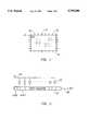
- FIG. 1is a plan view of a semiconductor chip including a code mechanism in accordance with the invention.
- FIG. 2is a functional block diagram of a code mechanism in accordance with one embodiment of the invention.
- FIG. 3is a plan view of a fuse which can be used in the code mechanism of FIG. 2.
- FIG. 4is a section view of an antifuse which can be used in the code mechanism of FIG. 2.
- FIG. 5is a functional block diagram of a code mechanism in accordance with an other embodiment of the invention.
- FIG. 6is a functional block diagram of an electrically erasable field effect transistor which can be used in the code mechanism of FIG. 5.
- FIG. 7is a functional block diagram of another embodiment of a code mechanism in accordance with the mechanism.
- FIG. 1is a plan view of an integrated circuit 10 having a plurality of leads 12 extending from contacts on the periphery thereof.
- a code mechanism 14 in accordance with the inventionis provided in a peripheral portion of the chip 10 and is accessible by leads 16. The code mechanism is addressable from outside of the chip for identification of the chip and for enabling operation of the chip.
- FIG. 2is a functional block diagram of one embodiment of the code mechanism 14 in FIG. 1 in accordance with one embodiment of the invention.
- a shift register 20can be periodically loaded through an array 22 of fuses or antifuses by applying a voltage potential to the lead 17. After the shift register 20 is loaded, the register is read out on line 18 to identify a code established by the array 22 of fuses or antifuses.
- the array 22can establish a binary code, for example 32 fuses will establish 2 32 possible serial numbers for the integrated circuit. Thus, the serial number of the integrated circuit as established by the array 22 of fuses or antifuses is readily accessed through the leads 17 and 18.
- the leads 17 and 18can also function as input and output leads for the integrated circuit 10 during normal circuit operation.
- FIG. 3is a plan view of a conventional fuse as employed in programming integrated circuits.
- an N-well 30is first established in the surface of the integrated circuit to provide isolation from the active regions of the circuit.
- a metal 1 ringis formed over an N+ guard ring to offer further electrical isolation.
- a metal 2 fuse line 34passes over the metal 1/N+ guard ring 32 and is normally conductive. However, the fuse is readily blown during circuit fabrication by applying a laser beam to the aluminum fuse line 34 within the guard ring 32 to ablate the line and open the connection provided by the fuse line.
- FIG. 4is a section view of an antifuse as disclosed in U.S. Pat. No. 4,590,589 which is normally nonconductive until a sufficient voltage is applied across the antifuse to lower the resistance thereof and become conductive.
- the antifusecan comprise a portion of an N-silicon substrate 40 with an implanted region 42 formed in a surface region by the introduction of P-type ions.
- the implanted ionsdisrupt the crystalline structure of the substrate 40, referred to as amorphotizing, and the disrupted crystalline structure increases the resistance between region 42 and the substrate 40.
- the crystalline state of the regionis reinstated and the resistance thereof drops appreciably.
- FIG. 5is a functional block diagram of another embodiment of the code mechanism in accordance with the invention which can be used to selectively enable the integrated circuit by loading a code word into shift register 50.
- a programmable shift register 52similar to the shift register of FIG. 2 for example, is used to store the code, and a comparator 54 receives and compares the programmed code with the code from shift register 50. When the codes match, comparator 54 provides a signal to activate the circuit. When the codes do not match, the circuit is disabled. Thus, the integrated circuit can limit the access to secured information unless a prescribed code is used to activate the circuit.
- an electrically erasable field effect transistor as shown in FIG. 6can be used to selectively load the programmable shift register 52.
- the field effect transistor of FIG. 6can be rendered conductive or nonconductive by the selective introduction of charge on a floating gate 60 between the control gate 62 and the channel region 64 of the transistor.
- the charge on the floating gateis typically applied by hot electron injection from either the source or drain into the floating gate by selective biasing of the transistor elements. Erasure of the floating gate occurs by electron tunneling from the floating gate to a suitably biased drain region.
- a thin tunneling oxideis typically provided under the floating gate 60 near the drain region.
- FIG. 7is a functional block diagram of another embodiment of a code mechanism in accordance with the invention.
- a shift register (or RAM) 70is again loaded and then used to address a ROM 72 which houses a table of encryption keys.
- the address of a suitable encryption keyis required so that the key from ROM 72 can be applied to encryption logic 74 for activating the integrated circuit.
- the address in the RAM or registercan be changed by writing a new address to the register from either a key panel on the outside of the chip or through downloading a new address from a transmission medium. This enables the encryption key to be regularly altered to avoid pirating.
- RAM and ROM structurescan be easily built in ASIC gate arrays and cell based logic processes and do not require the extra processing step required for fuse, antifuse, or EEPROM technology. Thus, the cost of this embodiment is lower.
Landscapes
- Engineering & Computer Science (AREA)
- Computer Security & Cryptography (AREA)
- Computer Networks & Wireless Communication (AREA)
- Signal Processing (AREA)
- Semiconductor Integrated Circuits (AREA)
- Semiconductor Memories (AREA)
Abstract
Description
Claims (11)
Priority Applications (1)
| Application Number | Priority Date | Filing Date | Title |
|---|---|---|---|
| US08/502,300US5799080A (en) | 1995-07-13 | 1995-07-13 | Semiconductor chip having identification/encryption code |
Applications Claiming Priority (1)
| Application Number | Priority Date | Filing Date | Title |
|---|---|---|---|
| US08/502,300US5799080A (en) | 1995-07-13 | 1995-07-13 | Semiconductor chip having identification/encryption code |
Publications (1)
| Publication Number | Publication Date |
|---|---|
| US5799080Atrue US5799080A (en) | 1998-08-25 |
Family
ID=23997203
Family Applications (1)
| Application Number | Title | Priority Date | Filing Date |
|---|---|---|---|
| US08/502,300Expired - LifetimeUS5799080A (en) | 1995-07-13 | 1995-07-13 | Semiconductor chip having identification/encryption code |
Country Status (1)
| Country | Link |
|---|---|
| US (1) | US5799080A (en) |
Cited By (17)
| Publication number | Priority date | Publication date | Assignee | Title |
|---|---|---|---|---|
| US5881155A (en)* | 1996-04-01 | 1999-03-09 | Schlumberger Industries | Security device for a semiconductor chip |
| US6289455B1 (en) | 1999-09-02 | 2001-09-11 | Crypotography Research, Inc. | Method and apparatus for preventing piracy of digital content |
| EP1170754A1 (en)* | 2000-07-03 | 2002-01-09 | Infineon Technologies AG | Chip-ID-register device |
| US6367042B1 (en)* | 1998-12-11 | 2002-04-02 | Lsi Logic Corporation | Testing methodology for embedded memories using built-in self repair and identification circuitry |
| US6456554B1 (en)* | 1999-10-19 | 2002-09-24 | Texas Instruments Incorporated | Chip identifier and method of fabrication |
| US6545926B2 (en)* | 1998-06-18 | 2003-04-08 | Mitsubishi Denki Kabushiki Kaisha | Antifuse address detecting circuit programmable by applying a high voltage and semiconductor integrated circuit device provided with the same |
| US20030144760A1 (en)* | 2000-01-20 | 2003-07-31 | Efraim Mangell | Personalized hardware |
| US6717222B2 (en) | 2001-10-07 | 2004-04-06 | Guobiao Zhang | Three-dimensional memory |
| US20040146163A1 (en)* | 2002-10-28 | 2004-07-29 | Nokia Corporation | Device keys |
| US20040165725A1 (en)* | 2003-02-20 | 2004-08-26 | Nishit Kumar | Unique identifier per chip for digital audio/video data encryption/decryption in personal video recorders |
| US6990387B1 (en)* | 2000-05-18 | 2006-01-24 | Intel Corporation | Test system for identification and sorting of integrated circuit devices |
| US6992433B2 (en)* | 2000-02-28 | 2006-01-31 | Ricoh Company, Ltd. | Electron-emitting device and image display apparatus using the same |
| US20070103063A1 (en)* | 2005-11-09 | 2007-05-10 | Kim Eun-Ah | Organic light emitting display device |
| US20090267636A1 (en)* | 2008-04-29 | 2009-10-29 | Samsung Electronics Co., Ltd. | Security circuit having an electrical fuse ROM |
| US20100250943A1 (en)* | 2009-03-27 | 2010-09-30 | International Business Machines Corporation | Method for security in electronically fused encryption keys |
| TWI483139B (en)* | 2011-12-29 | 2015-05-01 | 英特爾股份有限公司 | Secure key storage using physically unclonable functions |
| US9042551B2 (en) | 2012-06-04 | 2015-05-26 | International Business Machines Corporation | Electronically programmable fuse security encryption |
Citations (3)
| Publication number | Priority date | Publication date | Assignee | Title |
|---|---|---|---|---|
| US4404654A (en)* | 1980-01-29 | 1983-09-13 | Sharp Kabushiki Kaisha | Semiconductor device system |
| US5119163A (en)* | 1990-06-22 | 1992-06-02 | Sharp Kabushiki Kaisha | Semiconductor device |
| US5467396A (en)* | 1993-10-27 | 1995-11-14 | The Titan Corporation | Tamper-proof data storage |
- 1995
- 1995-07-13USUS08/502,300patent/US5799080A/ennot_activeExpired - Lifetime
Patent Citations (3)
| Publication number | Priority date | Publication date | Assignee | Title |
|---|---|---|---|---|
| US4404654A (en)* | 1980-01-29 | 1983-09-13 | Sharp Kabushiki Kaisha | Semiconductor device system |
| US5119163A (en)* | 1990-06-22 | 1992-06-02 | Sharp Kabushiki Kaisha | Semiconductor device |
| US5467396A (en)* | 1993-10-27 | 1995-11-14 | The Titan Corporation | Tamper-proof data storage |
Cited By (41)
| Publication number | Priority date | Publication date | Assignee | Title |
|---|---|---|---|---|
| US5881155A (en)* | 1996-04-01 | 1999-03-09 | Schlumberger Industries | Security device for a semiconductor chip |
| US6545926B2 (en)* | 1998-06-18 | 2003-04-08 | Mitsubishi Denki Kabushiki Kaisha | Antifuse address detecting circuit programmable by applying a high voltage and semiconductor integrated circuit device provided with the same |
| US6367042B1 (en)* | 1998-12-11 | 2002-04-02 | Lsi Logic Corporation | Testing methodology for embedded memories using built-in self repair and identification circuitry |
| US9569628B2 (en) | 1999-09-02 | 2017-02-14 | Cryptography Research, Inc. | Specialized circuitry for cryptographic authentication and other purposes |
| US6289455B1 (en) | 1999-09-02 | 2001-09-11 | Crypotography Research, Inc. | Method and apparatus for preventing piracy of digital content |
| US20060184807A1 (en)* | 1999-09-02 | 2006-08-17 | Kocher Paul C | Specialized circuitry for cryptographic authentication and other purposes |
| US7039816B2 (en) | 1999-09-02 | 2006-05-02 | Cryptography Research, Inc. | Using smartcards or other cryptographic modules for enabling connected devices to access encrypted audio and visual content |
| US20040111631A1 (en)* | 1999-09-02 | 2004-06-10 | Kocher Paul C. | Using smartcards or other cryptographic modules for enabling connected devices to access encrypted audio and visual content |
| US6640305B2 (en) | 1999-09-02 | 2003-10-28 | Cryptography Research, Inc. | Digital content protection method and apparatus |
| US6456554B1 (en)* | 1999-10-19 | 2002-09-24 | Texas Instruments Incorporated | Chip identifier and method of fabrication |
| US20030144760A1 (en)* | 2000-01-20 | 2003-07-31 | Efraim Mangell | Personalized hardware |
| US7884537B2 (en) | 2000-02-28 | 2011-02-08 | Ricoh Company, Ltd. | Pattern substrate including conductive pattern of overlapping circular patterns disposed on substrate |
| US20080138570A1 (en)* | 2000-02-28 | 2008-06-12 | Takuro Sekiya | Electron-emitting device and image display apparatus using the same |
| US7355335B2 (en) | 2000-02-28 | 2008-04-08 | Ricoh Company, Ltd. | Electron-emitting device and image display apparatus using the same |
| US6992433B2 (en)* | 2000-02-28 | 2006-01-31 | Ricoh Company, Ltd. | Electron-emitting device and image display apparatus using the same |
| US20060028118A1 (en)* | 2000-02-28 | 2006-02-09 | Takuro Sekiya | Electron-emitting device and image display apparatus using the same |
| US6990387B1 (en)* | 2000-05-18 | 2006-01-24 | Intel Corporation | Test system for identification and sorting of integrated circuit devices |
| US6496423B2 (en) | 2000-07-03 | 2002-12-17 | Infineon Technologies Ag | Chip ID register configuration |
| EP1170754A1 (en)* | 2000-07-03 | 2002-01-09 | Infineon Technologies AG | Chip-ID-register device |
| US7316934B2 (en) | 2000-12-18 | 2008-01-08 | Zavitan Semiconductors, Inc. | Personalized hardware |
| US6717222B2 (en) | 2001-10-07 | 2004-04-06 | Guobiao Zhang | Three-dimensional memory |
| US7920706B2 (en)* | 2002-10-28 | 2011-04-05 | Nokia Corporation | Method and system for managing cryptographic keys |
| US20040146163A1 (en)* | 2002-10-28 | 2004-07-29 | Nokia Corporation | Device keys |
| US20080119956A1 (en)* | 2002-12-16 | 2008-05-22 | Efraim Mangell | Personalized hardware |
| WO2004075546A3 (en)* | 2003-02-20 | 2004-12-23 | Zoran Corp | Unique identifier per chip for digital audio/video data encryption/decryption in personal video recorders |
| US20040165725A1 (en)* | 2003-02-20 | 2004-08-26 | Nishit Kumar | Unique identifier per chip for digital audio/video data encryption/decryption in personal video recorders |
| US8705733B2 (en) | 2003-02-20 | 2014-04-22 | Csr Technology Inc. | Unique identifier per chip for digital audio/video data encryption/decryption in personal video recorders |
| US7835520B2 (en)* | 2003-02-20 | 2010-11-16 | Zoran Corporation | Unique identifier per chip for digital audio/video data encryption/decryption in personal video recorders |
| US20110058669A1 (en)* | 2003-02-20 | 2011-03-10 | Zoran Corporation | Unique identifier per chip for digital audio/video data encryption/decryption in personal video recorders |
| US7919918B2 (en)* | 2005-11-09 | 2011-04-05 | Samsung Mobile Display Co., Ltd. | Organic light emitting display device |
| US20070103063A1 (en)* | 2005-11-09 | 2007-05-10 | Kim Eun-Ah | Organic light emitting display device |
| US7949136B2 (en) | 2008-04-29 | 2011-05-24 | Samsung Electronics Co., Ltd. | Security circuit having an electrical fuse ROM |
| US20110199809A1 (en)* | 2008-04-29 | 2011-08-18 | Samsung Electronics Co., Ltd. | Security circuit having an electrical fuse rom |
| US8258809B2 (en) | 2008-04-29 | 2012-09-04 | Samsung Electronics Co., Ltd. | Security circuit having an electrical fuse ROM |
| US20090267636A1 (en)* | 2008-04-29 | 2009-10-29 | Samsung Electronics Co., Ltd. | Security circuit having an electrical fuse ROM |
| US8230495B2 (en) | 2009-03-27 | 2012-07-24 | International Business Machines Corporation | Method for security in electronically fused encryption keys |
| US20100250943A1 (en)* | 2009-03-27 | 2010-09-30 | International Business Machines Corporation | Method for security in electronically fused encryption keys |
| TWI483139B (en)* | 2011-12-29 | 2015-05-01 | 英特爾股份有限公司 | Secure key storage using physically unclonable functions |
| US9544141B2 (en) | 2011-12-29 | 2017-01-10 | Intel Corporation | Secure key storage using physically unclonable functions |
| US10284368B2 (en) | 2011-12-29 | 2019-05-07 | Intel Corporation | Secure key storage |
| US9042551B2 (en) | 2012-06-04 | 2015-05-26 | International Business Machines Corporation | Electronically programmable fuse security encryption |
Similar Documents
| Publication | Publication Date | Title |
|---|---|---|
| US5799080A (en) | Semiconductor chip having identification/encryption code | |
| US5119163A (en) | Semiconductor device | |
| EP0227549B1 (en) | Semiconductor memory device including read only memory element for storing fixed information | |
| US7136319B2 (en) | Reduced area, reduced programming voltage CMOS eFUSE-based scannable non-volatile memory bitcell | |
| US5811869A (en) | Laser antifuse using gate capacitor | |
| EP0336500B1 (en) | Integrated circuit comprising a programmable cell | |
| AU621440B2 (en) | Prevention of alteration of data stored in secure integrated circuit chip memory | |
| US6222764B1 (en) | Erasable memory device and an associated method for erasing a memory cell therein | |
| GB2276254A (en) | Protecting data storage devices | |
| US6611040B2 (en) | Anti-fuse structure of writing and reading in integrated circuits | |
| US6266271B1 (en) | Nonvolatile semiconductor memory for preventing unauthorized copying | |
| JPS63175300A (en) | Semiconductor integrated circuit device | |
| US4656609A (en) | Semiconductor memory device | |
| EP1454323B1 (en) | Half density rom embedded dram | |
| US6781887B2 (en) | Anti-fuse structure and method of writing and reading in integrated circuits | |
| US5383162A (en) | Semiconductor memory device | |
| US5420817A (en) | Semiconductor integrated circuit device comprising memory area in which structurally different memory cells are included | |
| EP1340262A2 (en) | Poly fuse rom with mos device based cell structure and the method for read and write therefore | |
| US5247476A (en) | Semiconductor memory device having a mask rom and a prom | |
| US6002609A (en) | Semiconductor device having a security circuit for preventing illegal access | |
| KR100616720B1 (en) | How to Program a Fixed Memory Cell Device | |
| US20040027877A1 (en) | Method for setting the threshold voltage of a field-effect transistor, field-effect transistor and integrated circuit | |
| US6225829B1 (en) | device signature generator | |
| EP0194090A2 (en) | Programmable data security circuit for programmable logic device | |
| JPS6267798A (en) | Semiconductor integrated circuit device |
Legal Events
| Date | Code | Title | Description |
|---|---|---|---|
| AS | Assignment | Owner name:LSI LOGIC CORPORATION, CALIFORNIA Free format text:ASSIGNMENT OF ASSIGNORS INTEREST;ASSIGNORS:PADMANABHAN, GOBI R.;ZELAYETA, JOSEPH M.;YEGNASHANKARAN, VISVAMOHAN;AND OTHERS;REEL/FRAME:007829/0636;SIGNING DATES FROM 19950627 TO 19950711 | |
| STCF | Information on status: patent grant | Free format text:PATENTED CASE | |
| FPAY | Fee payment | Year of fee payment:4 | |
| FPAY | Fee payment | Year of fee payment:8 | |
| FEPP | Fee payment procedure | Free format text:PAYOR NUMBER ASSIGNED (ORIGINAL EVENT CODE: ASPN); ENTITY STATUS OF PATENT OWNER: LARGE ENTITY Free format text:PAYER NUMBER DE-ASSIGNED (ORIGINAL EVENT CODE: RMPN); ENTITY STATUS OF PATENT OWNER: LARGE ENTITY | |
| FPAY | Fee payment | Year of fee payment:12 | |
| AS | Assignment | Owner name:DEUTSCHE BANK AG NEW YORK BRANCH, AS COLLATERAL AG Free format text:PATENT SECURITY AGREEMENT;ASSIGNORS:LSI CORPORATION;AGERE SYSTEMS LLC;REEL/FRAME:032856/0031 Effective date:20140506 | |
| AS | Assignment | Owner name:LSI CORPORATION, CALIFORNIA Free format text:CHANGE OF NAME;ASSIGNOR:LSI LOGIC CORPORATION;REEL/FRAME:033102/0270 Effective date:20070406 | |
| AS | Assignment | Owner name:AVAGO TECHNOLOGIES GENERAL IP (SINGAPORE) PTE. LTD Free format text:ASSIGNMENT OF ASSIGNORS INTEREST;ASSIGNOR:LSI CORPORATION;REEL/FRAME:035390/0388 Effective date:20140814 | |
| AS | Assignment | Owner name:AGERE SYSTEMS LLC, PENNSYLVANIA Free format text:TERMINATION AND RELEASE OF SECURITY INTEREST IN PATENT RIGHTS (RELEASES RF 032856-0031);ASSIGNOR:DEUTSCHE BANK AG NEW YORK BRANCH, AS COLLATERAL AGENT;REEL/FRAME:037684/0039 Effective date:20160201 Owner name:LSI CORPORATION, CALIFORNIA Free format text:TERMINATION AND RELEASE OF SECURITY INTEREST IN PATENT RIGHTS (RELEASES RF 032856-0031);ASSIGNOR:DEUTSCHE BANK AG NEW YORK BRANCH, AS COLLATERAL AGENT;REEL/FRAME:037684/0039 Effective date:20160201 |