US5798967A - Sensing scheme for non-volatile memories - Google Patents
Sensing scheme for non-volatile memoriesDownload PDFInfo
- Publication number
- US5798967A US5798967AUS08/801,414US80141497AUS5798967AUS 5798967 AUS5798967 AUS 5798967AUS 80141497 AUS80141497 AUS 80141497AUS 5798967 AUS5798967 AUS 5798967A
- Authority
- US
- United States
- Prior art keywords
- coupled
- transistor
- bit line
- voltage
- circuit
- Prior art date
- Legal status (The legal status is an assumption and is not a legal conclusion. Google has not performed a legal analysis and makes no representation as to the accuracy of the status listed.)
- Expired - Lifetime
Links
Images


Classifications
- G—PHYSICS
- G11—INFORMATION STORAGE
- G11C—STATIC STORES
- G11C7/00—Arrangements for writing information into, or reading information out from, a digital store
- G11C7/06—Sense amplifiers; Associated circuits, e.g. timing or triggering circuits
- G11C7/067—Single-ended amplifiers
- G—PHYSICS
- G11—INFORMATION STORAGE
- G11C—STATIC STORES
- G11C16/00—Erasable programmable read-only memories
- G11C16/02—Erasable programmable read-only memories electrically programmable
- G11C16/06—Auxiliary circuits, e.g. for writing into memory
- G11C16/26—Sensing or reading circuits; Data output circuits
Definitions
- This inventionrelates generally to arrays of non-volatile memory cells and specifically to circuits for sensing whether such memory cells are in a programmed state or in an erased state.
- Conventional sensing circuitstypically determine whether a non-volatile memory cell is in a programmed state or an erased state by comparing the difference between the channel current in the cell selected for reading with the channel current in a reference cell.
- the reference cellis typically of a size and characteristics such that the reference cell conducts a channel current approximately one half of the channel current of the memory cell. For instance, a reference cell conducts 50 microamps of channel current and a programmed memory cell conducts 100 microamps of channel current.
- a read voltageis applied to the respective control gates of the selected memory cell and the reference cell. The resulting channel currents in the selected memory cell and the reference cell are then converted to a differential voltage indicative of the binary state of the memory cell.
- FIG. 1A conventional sensing circuit 10 operating in accordance with that described above is shown in FIG. 1 and described below with reference to a bit addressable memory array 50 containing a plurality PMOS memory cells 52.
- Cells 52each of which includes a P-channel select transistor 52a and a P-channel floating gate storage transistor 52b, in a common column are coupled to an associated one of bit lines BLx.
- Cells 52may be of the type disclosed in the above-referenced co-pending Patent Application entitled "A PMOS Memory Cell with Hot Electron Injection Programming and Tunnelling Erasing". When in a programmed state, cells 52 typically conduct approximately 100 microamps.
- Array 50includes reference cells 54 coupled to one or more associated reference bit lines DBLX.
- Reference cells 54each of which includes a P-channel select transistor 54a and a P-channel floating gate transistor 54b, remain in a state so as to conduct approximately 50 microamps of channel current. Note that page buffers and other appropriate address decode circuitry have been omitted from array 50 for clarity.
- select transistors 52a and reference transistors 54a in a common roware coupled to a select gate line SGO and the gates of cells 52b and reference cells 54b in a common row are coupled to a word line WL0 (only two rows of array 50 are shown for simplicity).
- the sources of each of storage transistors 52b and 54bare coupled to a common source node CS.
- the selected bit lines BLx of array 50are coupled to a sensing node SNODE via the decode circuitry (not shown) and an access transistor T3.
- SNODEis coupled to ground potential through a diode-connected transistor T4.
- the reference bit lines DBLXare coupled to a reference node REFNODE via an access transistor T5.
- REFNODEis coupled to ground potential through a diode-connected transistor T6.
- PMOS transistor T10in response to an enabling signal EN, sources current to the current mirror formed by transistors T8 and T9, thereby establishing bias currents in differential transistors T1 and T2.
- the source of transistor T1hereinafter referred to as output node OUT, is coupled to a conventional latch circuit 12.
- a bias transistor T7is coupled across the gates of transistors T1 and T2 and has a gate coupled to receive a control signal BIAS. Bias transistor T7 ensures that the gate voltages of transistors T1 and T2 are equal prior to reading operations, thereby "initializing" the differential input stage formed by transistors T1 and T2.
- Sensing circuit 10determines the binary state of a selected memory cell 52 as follows. During read operations, bit lines BLx and reference bit lines DBLX are discharged to approximately ground potential. A signal SG on line GS0 transitions to a low logic voltage to turn on select transistors 52a and reference select transistors 54a in the selected row. A signal CG on line CG0 transitions to a voltage approximately between ground potential and V CC . Reference cells 54b conduct a channel current so as to charge reference bit line DBL0 to a predetermined reference voltage V ref . If programmed, selected memory cell 52b conducts a channel current of approximately 100 microamps and charges its bit line BL0 to a high voltage, V H , where V H >V ref .
- transistor T2turns on harder than transistor T1, thereby allowing the output voltage OUT to rise above the trip point of latch circuit 12. As the voltage OUT exceeds the trip point, latch circuit 12 cause its output signal to transition logic states, thereby indicating that selected memory cell 52b is in an erased state.
- Sensing circuits of the type described abovehave several disadvantages.
- One such disadvantageis an undesirably low noise margin V noise .
- V noiseis equal to V D2 -V D1 and may be undesirably small so as to allow noise such as, for instance, ground bounce, to interfere with accurate transitions of differential pair transistors T1 and T2.
- Reference bit lines DBLx and associated reference cells 54are thus required in order to decrease the noise to an acceptable level.
- the inclusion of such reference bit lines and reference cellsundesirably increases the complexity, cost and surface area of an associated memory array such as, for instance, array 50.
- sensing circuit 10facilitates charging of the bit lines BLx by inducing channel current in selected memory cells 52.
- the reference bit linesare charged in a similar manner.
- the access time, or read speed, of a memory array associated with sensing circuit 10is dependent upon the channel current within the memory cells (and reference cells) of the memory array.
- reducing the size of the memory cellsresults in a lower channel current therein, reducing the size of the memory cells undesirably results in an increase in access time.
- increasing the number of memory cells per bit lineincreases the capacitance on the bit line and thus increases the time required to charge the bit line, increasing the size of the associated memory array also limits access time.
- a sensing circuitis disclosed herein which overcomes problems in the art described above.
- the sensing circuitcharges the bit lines of an associated memory array using one or more large-area pass transistors. In this manner, the read speed of the memory array is independent of the channel current of the memory cells within the memory array.
- a sink transistoris provided to sink a constant current from the selected bit lines during reading operations. This sink current is less than the channel current conducted by a selected memory cell of the memory array when the selected cell is in a programmed state and significantly improves the noise margin of the sensing circuit.
- sensing circuits in accordance with the present inventionallow for the elimination of reference cells and corresponding reference bit lines from the memory array associated with the sensing circuit.
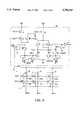
- FIG. 1includes a schematic diagram of a conventional sensing circuit
- FIG. 2includes a schematic diagram of a sensing circuit in accordance with the present invention.
- FIGS. 3A and 3Bare timing diagrams illustrating various node potentials of the sensing circuit shown in FIG. 2 during reading operations.
- a sensing circuit in accordance with the present inventionis described below in the context of a memory array 70 for clarity and convenience only; embodiments of the present invention are equally applicable for reading data from memory arrays containing other well known memory cells and having various other well known suitable array configurations. Further, it is to be understood that the description that follows is merely illustrative of the present invention and should not be construed in a limiting manner.
- sensing circuit 60is configured to determine the binary state of selected ones of memory cells 52 of bit-addressable memory array 70, where those elements common to the circuits of FIGS. 1 and 2 are similarly denoted.
- array 70contains neither reference bit lines nor reference cells. Note that page buffers and other appropriate address decode circuitry have been omitted from array 70 for clarity.
- the differential pair formed by transistors T1 and T2responds to differences between the voltage on a selected bit line BLx at SNODE and a predetermined reference voltage V ref at REFNODE.
- the bit lines BLx of memory array 70 and the drain of PMOS access transistor T3 of circuit 60are coupled together at a common node SRDX via the decode circuitry (not shown).
- the voltage at node SRDXi.e., the bit line voltage
- the gate of transistor T3is coupled to the output terminal of a NAND gate N1 having a first input terminal coupled to node SRDX and a second input terminal coupled to receive a select address signal SAD.
- Coupled between the gate of transistor T1 and ground potentialare diode-connected transistor T4 and a constant current sink NMOS transistor T15.
- the gate of sink transistor T15is coupled to receive a bias signal IBIASN.
- the gate of transistor T2is coupled to ground via diode-connected transistor T6.
- a PMOS bias transistor T11is coupled between the gate of transistor T2 and V CC , and has a gate coupled to receive a bias signal IBIASP. As will be explained below, the signal IBIASP sets up reference voltage V ref at the gate of transistor T2.
- the source of an NMOS transistor T12 and the drain a PMOS transistor T13are coupled to the source of access transistor T3 and thus to node SRDX.
- the source of transistor T13is coupled to ground potential, and the gate of transistor T13 is coupled to receive a reference voltage V ref1 .
- the drain of an NMOS transistor T12is coupled to the source of an NMOS pass transistor T14, and the gate of transistor T12 is coupled to receive a reference voltage V ref2 .
- V ref1 and V ref2are approximately 1.2 volts and approximately 2.2 volts, respectively.
- the gate of pass transistor T14is coupled to receive an address transition detection signal ATD, and the drain of transistor T14 is coupled to V CC .
- circuit 60The operation of circuit 60 is as follows. Signal IBIASP induces a current I 6 of approximately 2 microamps in transistor T11 and diode-connected transistor T6 which, in turn, results in V ref being equal to approximately 0.8 volts. In other embodiments, transistors T6 and T11 may be replaced by other suitable reference circuits.
- latch 12With the voltage at SNODE equal to approximately 1.5 volts and the voltage at REFNODE equal to approximately 0.8 volts, transistor T3 turns on much harder than transistor T4, thereby pulling the trip voltage V trip at the drain of transistor T1 towards ground potential. In response thereto, latch 12 outputs a logic low signal. Note that in other embodiments latch 12 may be replaced by any suitable circuit which transitions the logic state of its output signal in response to the trip voltage V trip crossing a predetermined threshold voltage.
- transistor T4is a large area transistor capable of conducting a current on the order of a few hundred amps.
- Appropriate read voltagesare provided on select line SL0, word line WL0, and to common source CS of memory array 70. Such read voltages are disclosed, for instance, in the above-referenced patent application entitled "A PMOS Memory Cell with Hot Electron Injection Programming and Tunnelling Erasing".
- the one of cells 52 selected for reading by the address decode circuitrysources approximately 10 microamps to SNODE via selected bit line BLx so as to prevent SNODE from discharging below approximately 0.9 volts.
- the voltage at SNODEremains higher than the voltage at REFNODE and, as a result, voltage V trip remains below the threshold of latch 12. Accordingly, latch 12 continues to output a logic low signal, thereby indicating that the selected one of cells 52 is in a programmed state.
- the potentials of SNODE and signal ATD when selected cell 52 is in a programmed stateare shown in FIG. 3A.
- transistor T15is preferably of a size to conduct a current I 15 of approximately between 3-4 microamps and is biased by a well known bandgap referenced current mirror. If the current through the selected cell 52 is greater than I 6 +I 15 , latch 12 will output a logic low signal indicative of selected cell 52 being in a programmed state and, conversely, if the current through the selected cell 52 is less than I 6 +I 15 , latch 12 will output a logic high signal indicative of selected cell 52 being in a erased state.
- transistor T15allows SNODE to discharge more quickly to ground potential, thereby compensating for limiting of the discharge rate of SNODE caused by the turning off transistor T4 when SNODE approaches 0.7 volts.
- V noiseThe noise margin for circuit 70, V noise , may be expressed as:
- V Tis the threshold voltage of transistors T4 and T6
- V D1is the underdrive voltage on the gate of transistor T4 when selected cell 52 in an erased state
- V D2is the overdrive voltage on the gate of transistor T4 when selected cell 52 in a programmed state.
- a transistor T16is coupled between the drain of transistor T1 and ground potential and has a gate coupled to receive signal EN. Transistor T16 ensures that during the first portion of the read cycle, i.e, when bit lines BLx are charged to approximately 1.5 volts by transistors T12 and T14, the trip voltage V trip remains at ground potential and thereby ensures that the differential pair T1 and T2 is properly calibrated.
Landscapes
- Read Only Memory (AREA)
Abstract
Description
V.sub.T +V.sub.D2 -(V.sub.T -V.sub.D1)=V.sub.D2 +V.sub.D1
Claims (19)
Priority Applications (2)
| Application Number | Priority Date | Filing Date | Title |
|---|---|---|---|
| US08/801,414US5798967A (en) | 1997-02-22 | 1997-02-22 | Sensing scheme for non-volatile memories |
| TW087113987ATW440849B (en) | 1997-02-22 | 1998-08-25 | Sensing scheme for non-volatile memories |
Applications Claiming Priority (1)
| Application Number | Priority Date | Filing Date | Title |
|---|---|---|---|
| US08/801,414US5798967A (en) | 1997-02-22 | 1997-02-22 | Sensing scheme for non-volatile memories |
Publications (1)
| Publication Number | Publication Date |
|---|---|
| US5798967Atrue US5798967A (en) | 1998-08-25 |
Family
ID=25181035
Family Applications (1)
| Application Number | Title | Priority Date | Filing Date |
|---|---|---|---|
| US08/801,414Expired - LifetimeUS5798967A (en) | 1997-02-22 | 1997-02-22 | Sensing scheme for non-volatile memories |
Country Status (2)
| Country | Link |
|---|---|
| US (1) | US5798967A (en) |
| TW (1) | TW440849B (en) |
Cited By (24)
| Publication number | Priority date | Publication date | Assignee | Title |
|---|---|---|---|---|
| US6115290A (en)* | 1998-04-29 | 2000-09-05 | Intel Corporation | Mechanism for resetting sense circuitry to a known state in a nonvolatile memory device |
| US6198661B1 (en)* | 1998-11-26 | 2001-03-06 | Hyundai Electronics Industries Co., Ltd. | Sensing circuit for semiconductor device and sensing method using the same |
| US6407588B1 (en)* | 2000-08-28 | 2002-06-18 | Micron Technology, Inc. | High speed low power input buffer |
| US20030021154A1 (en)* | 2001-02-22 | 2003-01-30 | Yeong-Taek Lee | Bit line setup and discharge circuit for programming non-volatile memory |
| US20030206437A1 (en)* | 1995-03-07 | 2003-11-06 | California Institute Of Technology, A California Non-Profit Corporation | Floating-gate semiconductor structures |
| US20040037127A1 (en)* | 2002-07-05 | 2004-02-26 | Impinj, Inc., A Delaware Corporation | Differential floating gate nonvolatile memories |
| US20040178829A1 (en)* | 2003-03-14 | 2004-09-16 | Wang Shiou-Yu Alex | Sense amplifier circuit and method |
| US20050063235A1 (en)* | 2002-07-05 | 2005-03-24 | Impinj, Inc., A Delaware Corporation | PFET nonvolatile memory |
| US20060221715A1 (en)* | 2005-03-31 | 2006-10-05 | Impinj, Inc. | Redundant non-volatile memory cell |
| US20060285391A1 (en)* | 2005-06-20 | 2006-12-21 | Raul-Adrian Cernea | Compensation currents in non-volatile memory read operations |
| US20070263456A1 (en)* | 2005-03-17 | 2007-11-15 | Impinj, Inc. | Inverter non-volatile memory cell and array system |
| US20080019173A1 (en)* | 2006-07-20 | 2008-01-24 | Yan Li | System for configuring compensation |
| US20080019193A1 (en)* | 2006-07-20 | 2008-01-24 | Yan Li | Compensating for coupling based on sensing a neighbor using coupling |
| US20080019175A1 (en)* | 2006-07-20 | 2008-01-24 | Yan Li | System that compensates for coupling based on sensing a neighbor using coupling |
| US20080019185A1 (en)* | 2006-07-20 | 2008-01-24 | Yan Li | Compensating for coupling during programming |
| US20080019186A1 (en)* | 2006-07-20 | 2008-01-24 | Yan Li | System that compensates for coupling during programming |
| US20080019174A1 (en)* | 2006-07-20 | 2008-01-24 | Yan Li | Method for configuring compensation |
| US20080123404A1 (en)* | 2006-11-17 | 2008-05-29 | Stmicroelectronics S.R.L. | Reading voltage generator for a non-volatile eeprom memory cell matrix of a semiconductor device and corresponding manufacturing process |
| US20080175050A1 (en)* | 2004-05-05 | 2008-07-24 | Alberto Pesavento | Pfet nonvolatile memory |
| US20080205150A1 (en)* | 2004-04-21 | 2008-08-28 | Impinj, Inc. | Hybrid non-volatile memory |
| US7796450B1 (en) | 2007-04-24 | 2010-09-14 | Virage Logic Corporation | Radio frequency (RFID) tag including configurable single bit/dual bits memory |
| US8102007B1 (en) | 2001-08-13 | 2012-01-24 | Synopsys, Inc. | Apparatus for trimming high-resolution digital-to-analog converter |
| US8122307B1 (en) | 2006-08-15 | 2012-02-21 | Synopsys, Inc. | One time programmable memory test structures and methods |
| US8139411B1 (en) | 2008-05-22 | 2012-03-20 | Synopsys, Inc. | pFET nonvolatile memory |
Citations (10)
| Publication number | Priority date | Publication date | Assignee | Title |
|---|---|---|---|---|
| US5138579A (en)* | 1987-07-31 | 1992-08-11 | Kabushiki Kaisha Toshiba | Semiconductor memory device having transfer gates which prevent high voltages from being applied to memory and dummy cells in the reading operation |
| US5177707A (en)* | 1989-10-02 | 1993-01-05 | Sgs-Thomson Microelectronics S.A. | Memory with improved reading time |
| US5197023A (en)* | 1990-10-31 | 1993-03-23 | Nec Corporation | Hardware arrangement for floating-point addition and subtraction |
| US5353249A (en)* | 1992-01-30 | 1994-10-04 | Fujitsu Limited | Non-volatile semiconductor memory device |
| US5386158A (en)* | 1992-03-13 | 1995-01-31 | Silicon Storage Technology, Inc. | Sensing circuit for a floating gate memory device |
| US5390147A (en)* | 1994-03-02 | 1995-02-14 | Atmel Corporation | Core organization and sense amplifier having lubricating current, active clamping and buffered sense node for speed enhancement for non-volatile memory |
| US5428570A (en)* | 1992-05-28 | 1995-06-27 | Kabushiki Kaisha Toshiba | Nonvolatile semiconductor memory device |
| US5519652A (en)* | 1992-12-07 | 1996-05-21 | Fujitsu Limited | Nonvolatile semiconductor memory for positively holding stored data |
| US5559737A (en)* | 1991-07-25 | 1996-09-24 | Kabushiki Kaisha Toshiba | Nonvolatile semiconductor memory capable of simultaneously equalizing bit lines and sense lines |
| US5627790A (en)* | 1994-03-22 | 1997-05-06 | Sgs-Thomson Microelectronics S.R.L. | Reading circuit for an integrated semiconductor memory device |
- 1997
- 1997-02-22USUS08/801,414patent/US5798967A/ennot_activeExpired - Lifetime
- 1998
- 1998-08-25TWTW087113987Apatent/TW440849B/ennot_activeIP Right Cessation
Patent Citations (10)
| Publication number | Priority date | Publication date | Assignee | Title |
|---|---|---|---|---|
| US5138579A (en)* | 1987-07-31 | 1992-08-11 | Kabushiki Kaisha Toshiba | Semiconductor memory device having transfer gates which prevent high voltages from being applied to memory and dummy cells in the reading operation |
| US5177707A (en)* | 1989-10-02 | 1993-01-05 | Sgs-Thomson Microelectronics S.A. | Memory with improved reading time |
| US5197023A (en)* | 1990-10-31 | 1993-03-23 | Nec Corporation | Hardware arrangement for floating-point addition and subtraction |
| US5559737A (en)* | 1991-07-25 | 1996-09-24 | Kabushiki Kaisha Toshiba | Nonvolatile semiconductor memory capable of simultaneously equalizing bit lines and sense lines |
| US5353249A (en)* | 1992-01-30 | 1994-10-04 | Fujitsu Limited | Non-volatile semiconductor memory device |
| US5386158A (en)* | 1992-03-13 | 1995-01-31 | Silicon Storage Technology, Inc. | Sensing circuit for a floating gate memory device |
| US5428570A (en)* | 1992-05-28 | 1995-06-27 | Kabushiki Kaisha Toshiba | Nonvolatile semiconductor memory device |
| US5519652A (en)* | 1992-12-07 | 1996-05-21 | Fujitsu Limited | Nonvolatile semiconductor memory for positively holding stored data |
| US5390147A (en)* | 1994-03-02 | 1995-02-14 | Atmel Corporation | Core organization and sense amplifier having lubricating current, active clamping and buffered sense node for speed enhancement for non-volatile memory |
| US5627790A (en)* | 1994-03-22 | 1997-05-06 | Sgs-Thomson Microelectronics S.R.L. | Reading circuit for an integrated semiconductor memory device |
Cited By (76)
| Publication number | Priority date | Publication date | Assignee | Title |
|---|---|---|---|---|
| US20030206437A1 (en)* | 1995-03-07 | 2003-11-06 | California Institute Of Technology, A California Non-Profit Corporation | Floating-gate semiconductor structures |
| US20050104118A1 (en)* | 1995-03-07 | 2005-05-19 | California Institute Of Technology, A California Non-Profit Corporation | Floating-gate semiconductor structures |
| US20050104119A1 (en)* | 1995-03-07 | 2005-05-19 | California Institute Of Technology, A California Non-Profit Corporation | Floating-gate semiconductor structures |
| US7548460B2 (en) | 1995-03-07 | 2009-06-16 | California Institute Of Technology | Floating-gate semiconductor structures |
| US20050099859A1 (en)* | 1995-03-07 | 2005-05-12 | California Institute Of Technology, A California Non-Profit Corporation | Floating-gate semiconductor structures |
| US6965142B2 (en) | 1995-03-07 | 2005-11-15 | Impinj, Inc. | Floating-gate semiconductor structures |
| US7098498B2 (en) | 1995-03-07 | 2006-08-29 | California Institute Of Technology | Floating-gate semiconductor structures |
| US6115290A (en)* | 1998-04-29 | 2000-09-05 | Intel Corporation | Mechanism for resetting sense circuitry to a known state in a nonvolatile memory device |
| US6198661B1 (en)* | 1998-11-26 | 2001-03-06 | Hyundai Electronics Industries Co., Ltd. | Sensing circuit for semiconductor device and sensing method using the same |
| US6600343B2 (en) | 2000-08-28 | 2003-07-29 | Micron Technology, Inc. | High speed low power input buffer |
| US20050225364A1 (en)* | 2000-08-28 | 2005-10-13 | Micron Technology, Inc. | High speed low power input buffer |
| US6914454B2 (en) | 2000-08-28 | 2005-07-05 | Micron Technology, Inc. | High speed low power input buffer |
| US20040017231A1 (en)* | 2000-08-28 | 2004-01-29 | Micron Technology, Inc. | High speed low power input buffer |
| US6407588B1 (en)* | 2000-08-28 | 2002-06-18 | Micron Technology, Inc. | High speed low power input buffer |
| KR100454116B1 (en)* | 2001-02-22 | 2004-10-26 | 삼성전자주식회사 | Bit line setup and discharge circuit for programming non-volatile memory |
| US20030026145A1 (en)* | 2001-02-22 | 2003-02-06 | Yeong-Taek Lee | Bit line setup and discharge circuit for programming non-volatile memory |
| US6813187B2 (en) | 2001-02-22 | 2004-11-02 | Samsung Electronics Co., Ltd. | Bit line setup and discharge circuit for programming non-volatile memory |
| US7453729B2 (en) | 2001-02-22 | 2008-11-18 | Samsung Electronics Co., Ltd. | Bit line setup and discharge circuit for programming non-volatile memory |
| US7835191B2 (en) | 2001-02-22 | 2010-11-16 | Samsung Electronics Co., Ltd. | Bit line setup and discharge circuit for programming non-volatile memory |
| US20030021154A1 (en)* | 2001-02-22 | 2003-01-30 | Yeong-Taek Lee | Bit line setup and discharge circuit for programming non-volatile memory |
| US6751124B2 (en) | 2001-02-22 | 2004-06-15 | Samsung Electronics Co., Ltd. | Bit line setup and discharge circuit for programming non-volatile memory |
| US8102007B1 (en) | 2001-08-13 | 2012-01-24 | Synopsys, Inc. | Apparatus for trimming high-resolution digital-to-analog converter |
| US20040037127A1 (en)* | 2002-07-05 | 2004-02-26 | Impinj, Inc., A Delaware Corporation | Differential floating gate nonvolatile memories |
| US6950342B2 (en) | 2002-07-05 | 2005-09-27 | Impinj, Inc. | Differential floating gate nonvolatile memories |
| US7221596B2 (en) | 2002-07-05 | 2007-05-22 | Impinj, Inc. | pFET nonvolatile memory |
| US20050063235A1 (en)* | 2002-07-05 | 2005-03-24 | Impinj, Inc., A Delaware Corporation | PFET nonvolatile memory |
| US20040178829A1 (en)* | 2003-03-14 | 2004-09-16 | Wang Shiou-Yu Alex | Sense amplifier circuit and method |
| US6940315B2 (en) | 2003-03-14 | 2005-09-06 | Programmable Microelectronics Corporation | High speed sense amplifier for memory output |
| US20080205150A1 (en)* | 2004-04-21 | 2008-08-28 | Impinj, Inc. | Hybrid non-volatile memory |
| US8077511B2 (en) | 2004-04-21 | 2011-12-13 | Synopsys, Inc. | Hybrid non-volatile memory |
| US20080175050A1 (en)* | 2004-05-05 | 2008-07-24 | Alberto Pesavento | Pfet nonvolatile memory |
| US8111558B2 (en) | 2004-05-05 | 2012-02-07 | Synopsys, Inc. | pFET nonvolatile memory |
| US20070263456A1 (en)* | 2005-03-17 | 2007-11-15 | Impinj, Inc. | Inverter non-volatile memory cell and array system |
| US7791950B2 (en) | 2005-03-17 | 2010-09-07 | Virage Logic Corporation | Inverter non-volatile memory cell and array system |
| US20080136602A1 (en)* | 2005-03-31 | 2008-06-12 | Impinj, Inc. | Rfid tag with redundant non-volatile memory cell |
| US7808823B2 (en) | 2005-03-31 | 2010-10-05 | Virage Logic Corporation | RFID tag with redundant non-volatile memory cell |
| US20060221715A1 (en)* | 2005-03-31 | 2006-10-05 | Impinj, Inc. | Redundant non-volatile memory cell |
| US7679957B2 (en) | 2005-03-31 | 2010-03-16 | Virage Logic Corporation | Redundant non-volatile memory cell |
| US20070133298A1 (en)* | 2005-06-20 | 2007-06-14 | Raul-Adrian Cernea | Time-dependent compensation currents in non-volatile memory read operations |
| US20070133297A1 (en)* | 2005-06-20 | 2007-06-14 | Raul-Adrian Cernea | Non-volatile memory read operations using compensation currents |
| US7193898B2 (en) | 2005-06-20 | 2007-03-20 | Sandisk Corporation | Compensation currents in non-volatile memory read operations |
| US20080198656A1 (en)* | 2005-06-20 | 2008-08-21 | Raul-Adrian Cernea | Time-dependent compensation currents in non-volatile memory read operations |
| US20060285391A1 (en)* | 2005-06-20 | 2006-12-21 | Raul-Adrian Cernea | Compensation currents in non-volatile memory read operations |
| US7656713B2 (en) | 2005-06-20 | 2010-02-02 | Sandisk Corporation | Non-volatile memory read operations using compensation currents |
| US7379343B2 (en) | 2005-06-20 | 2008-05-27 | Sandisk Corporation | Time-dependent compensation currents in non-volatile memory read operations |
| US7535769B2 (en) | 2005-06-20 | 2009-05-19 | Sandisk Corporation | Time-dependent compensation currents in non-volatile memory read operations |
| US7400535B2 (en) | 2006-07-20 | 2008-07-15 | Sandisk Corporation | System that compensates for coupling during programming |
| US7969778B2 (en) | 2006-07-20 | 2011-06-28 | Sandisk Corporation | System that compensates for coupling based on sensing a neighbor using coupling |
| US20090003053A1 (en)* | 2006-07-20 | 2009-01-01 | Yan Li | System that compensates for coupling based on sensing a neighbor using coupling |
| US7480179B2 (en) | 2006-07-20 | 2009-01-20 | Sandisk Corporation | System that compensates for coupling during programming |
| US7495953B2 (en) | 2006-07-20 | 2009-02-24 | Sandisk Corporation | System for configuring compensation |
| US7506113B2 (en) | 2006-07-20 | 2009-03-17 | Sandisk Corporation | Method for configuring compensation |
| US7522454B2 (en) | 2006-07-20 | 2009-04-21 | Sandisk Corporation | Compensating for coupling based on sensing a neighbor using coupling |
| US7443729B2 (en) | 2006-07-20 | 2008-10-28 | Sandisk Corporation | System that compensates for coupling based on sensing a neighbor using coupling |
| US20080219056A1 (en)* | 2006-07-20 | 2008-09-11 | Yan Li | System that compensates for coupling during programming |
| US20090185416A1 (en)* | 2006-07-20 | 2009-07-23 | Yan Li | System that compensates for coupling based on sensing a neighbor using coupling |
| US7602647B2 (en) | 2006-07-20 | 2009-10-13 | Sandisk Corporation | System that compensates for coupling based on sensing a neighbor using coupling |
| US7616480B2 (en) | 2006-07-20 | 2009-11-10 | Sandisk Corp | System that compensates for coupling based on sensing a neighbor using coupling |
| US7630248B2 (en) | 2006-07-20 | 2009-12-08 | Sandisk Corporation | System that compensates for coupling during programming |
| US20080219051A1 (en)* | 2006-07-20 | 2008-09-11 | Yan Li | System that compensates for coupling during programming |
| US8411507B2 (en) | 2006-07-20 | 2013-04-02 | Sandisk Technologies Inc. | Compensating for coupling during programming |
| US8284606B2 (en) | 2006-07-20 | 2012-10-09 | Sandisk Technologies Inc. | Compensating for coupling during programming |
| US20100067296A1 (en)* | 2006-07-20 | 2010-03-18 | Yan Li | Compensating for coupling during programming |
| US20080019174A1 (en)* | 2006-07-20 | 2008-01-24 | Yan Li | Method for configuring compensation |
| US20080019173A1 (en)* | 2006-07-20 | 2008-01-24 | Yan Li | System for configuring compensation |
| US20080019186A1 (en)* | 2006-07-20 | 2008-01-24 | Yan Li | System that compensates for coupling during programming |
| US20080019185A1 (en)* | 2006-07-20 | 2008-01-24 | Yan Li | Compensating for coupling during programming |
| US7885119B2 (en) | 2006-07-20 | 2011-02-08 | Sandisk Corporation | Compensating for coupling during programming |
| US20090003052A1 (en)* | 2006-07-20 | 2009-01-01 | Yan Li | System that compensates for coupling based on sensing a neighbor using coupling |
| US20080019175A1 (en)* | 2006-07-20 | 2008-01-24 | Yan Li | System that compensates for coupling based on sensing a neighbor using coupling |
| US20080019193A1 (en)* | 2006-07-20 | 2008-01-24 | Yan Li | Compensating for coupling based on sensing a neighbor using coupling |
| US8122307B1 (en) | 2006-08-15 | 2012-02-21 | Synopsys, Inc. | One time programmable memory test structures and methods |
| US20080123404A1 (en)* | 2006-11-17 | 2008-05-29 | Stmicroelectronics S.R.L. | Reading voltage generator for a non-volatile eeprom memory cell matrix of a semiconductor device and corresponding manufacturing process |
| US7663927B2 (en)* | 2006-11-17 | 2010-02-16 | Stmicroelectronics S.R.L. | Reading voltage generator for a non-volatile EEPROM memory cell matrix of a semiconductor device and corresponding manufacturing process |
| US7796450B1 (en) | 2007-04-24 | 2010-09-14 | Virage Logic Corporation | Radio frequency (RFID) tag including configurable single bit/dual bits memory |
| US8139411B1 (en) | 2008-05-22 | 2012-03-20 | Synopsys, Inc. | pFET nonvolatile memory |
Also Published As
| Publication number | Publication date |
|---|---|
| TW440849B (en) | 2001-06-16 |
Similar Documents
| Publication | Publication Date | Title |
|---|---|---|
| US5798967A (en) | Sensing scheme for non-volatile memories | |
| KR100218244B1 (en) | Data reading circuit of nonvolatile semiconductor memory | |
| US5638326A (en) | Parallel page buffer verify or read of cells on a word line using a signal from a reference cell in a flash memory device | |
| EP1023731B1 (en) | Sense amplifier for flash memories | |
| EP0907955B1 (en) | A multiple bits-per-cell flash shift register page buffer | |
| US5428570A (en) | Nonvolatile semiconductor memory device | |
| US5594691A (en) | Address transition detection sensing interface for flash memory having multi-bit cells | |
| EP0477369B1 (en) | Semiconductor memory device | |
| EP0740307B1 (en) | Sense amplifier circuit for semiconductor memory devices | |
| CN101107671B (en) | Memory sensing circuit and method for low voltage operation | |
| US6788601B2 (en) | Semiconductor memory device and current mirror circuit | |
| US5982662A (en) | Semiconductor memory device with improved read characteristics for data having multi values | |
| EP0791936B1 (en) | Semiconductor memory device | |
| US6147910A (en) | Parallel read and verify for floating gate memory device | |
| US5293345A (en) | Semiconductor memory device having a data detection circuit with two reference potentials | |
| JP3615009B2 (en) | Semiconductor memory device | |
| US5191552A (en) | Semiconductor memory device with address transition actuated dummy cell | |
| WO1997005623A1 (en) | Flash memory system having reduced disturb and method | |
| US6166957A (en) | Nonvolatile semiconductor memory device with a level shifter circuit | |
| US6101126A (en) | Nonvolatile semiconductor memory device with a level shifter circuit | |
| KR100413997B1 (en) | Nonvolatile semiconductor memory | |
| US7221595B2 (en) | Semiconductor device and method of generating sense signal | |
| EP0405220B1 (en) | Semiconductor memory device | |
| KR100281799B1 (en) | Semiconductor memory device having circuitry for generating different word line voltages | |
| JP2595084B2 (en) | Semiconductor storage device |
Legal Events
| Date | Code | Title | Description |
|---|---|---|---|
| AS | Assignment | Owner name:PROGRAMMABLE MICROELECTRONICS CORPORATION, CALIFOR Free format text:ASSIGNMENT OF ASSIGNORS INTEREST;ASSIGNORS:SARIN, VISHAL;KOWSHIK, VIKRAM;TENG-FENG YU, ANDY;REEL/FRAME:008418/0989 Effective date:19970220 | |
| STCF | Information on status: patent grant | Free format text:PATENTED CASE | |
| FEPP | Fee payment procedure | Free format text:PAYOR NUMBER ASSIGNED (ORIGINAL EVENT CODE: ASPN); ENTITY STATUS OF PATENT OWNER: LARGE ENTITY | |
| FPAY | Fee payment | Year of fee payment:4 | |
| FEPP | Fee payment procedure | Free format text:PAT HOLDER NO LONGER CLAIMS SMALL ENTITY STATUS, ENTITY STATUS SET TO UNDISCOUNTED (ORIGINAL EVENT CODE: STOL); ENTITY STATUS OF PATENT OWNER: LARGE ENTITY | |
| REFU | Refund | Free format text:REFUND - PAYMENT OF MAINTENANCE FEE, 8TH YR, SMALL ENTITY (ORIGINAL EVENT CODE: R2552); ENTITY STATUS OF PATENT OWNER: LARGE ENTITY | |
| FPAY | Fee payment | Year of fee payment:8 | |
| SULP | Surcharge for late payment | Year of fee payment:7 | |
| AS | Assignment | Owner name:CHINGIS TECHNOLOGY CORPORATION, CALIFORNIA Free format text:CHANGE OF NAME;ASSIGNOR:PROGRAMMABLE MICROELECTRONICS CORP.;REEL/FRAME:017422/0868 Effective date:20060130 | |
| FPAY | Fee payment | Year of fee payment:12 |