US5798829A - Single laser bright field and dark field system for detecting anomalies of a sample - Google Patents
Single laser bright field and dark field system for detecting anomalies of a sampleDownload PDFInfo
- Publication number
- US5798829A US5798829AUS08/611,109US61110996AUS5798829AUS 5798829 AUS5798829 AUS 5798829AUS 61110996 AUS61110996 AUS 61110996AUS 5798829 AUS5798829 AUS 5798829A
- Authority
- US
- United States
- Prior art keywords
- sample
- beams
- incident
- light
- detecting
- Prior art date
- Legal status (The legal status is an assumption and is not a legal conclusion. Google has not performed a legal analysis and makes no representation as to the accuracy of the status listed.)
- Expired - Lifetime
Links
Images


Classifications
- G—PHYSICS
- G01—MEASURING; TESTING
- G01N—INVESTIGATING OR ANALYSING MATERIALS BY DETERMINING THEIR CHEMICAL OR PHYSICAL PROPERTIES
- G01N21/00—Investigating or analysing materials by the use of optical means, i.e. using sub-millimetre waves, infrared, visible or ultraviolet light
- G01N21/84—Systems specially adapted for particular applications
- G01N21/88—Investigating the presence of flaws or contamination
- G01N21/95—Investigating the presence of flaws or contamination characterised by the material or shape of the object to be examined
- G01N21/9501—Semiconductor wafers
- G—PHYSICS
- G01—MEASURING; TESTING
- G01N—INVESTIGATING OR ANALYSING MATERIALS BY DETERMINING THEIR CHEMICAL OR PHYSICAL PROPERTIES
- G01N21/00—Investigating or analysing materials by the use of optical means, i.e. using sub-millimetre waves, infrared, visible or ultraviolet light
- G01N21/84—Systems specially adapted for particular applications
- G01N21/88—Investigating the presence of flaws or contamination
- G01N21/8806—Specially adapted optical and illumination features
- G01N2021/8822—Dark field detection
- G01N2021/8825—Separate detection of dark field and bright field
Definitions
- This inventionrelates in general to systems for detecting anomalies of samples, and in particular to a single laser bright field and dark field system for detecting anomalies on samples such as semiconductor wafers, photomasks, reticles and ceramic tiles.
- semiconductor devices fabricated on silicon wafershas been continually reduced.
- semiconductor devicescan be fabricated at a resolution of a half micron or less, and 64 megabit DRAMS are being fabricated with a 0.35 micron design rule.
- the shrinking of semiconductor devices to smaller and smaller sizeshas imposed a much more stringent requirement on the sensitivity of wafer inspection instruments which are called upon to detect contaminant particles and surface defects that are small compared to the size of the semiconductor devices.
- it is useful also to know the structural characteristics of the defectsuch as whether a surface defect is an elevation or a depression in the surface.
- Many wafer inspection instrumentsare dark field systems, where light scattered on a surface is inspected to detect particles and surface defects.
- One of the problems in a dark field systemis that, due to the fact that information concerning structural characteristics of the defects may be lost because of the scattering, it may be difficult or impossible for dark field systems to determine the structural characteristics of the defects, such as whether the defect is an elevation or a depression in the surface. While it is possible for bright field systems to detect the structural characteristics of the defect, the ever present background signal can be many orders of magnitude larger than the feature related signal from the defect.
- This inventionis based on the observation that both dark field detection and bright field detection may be employed for detecting particles and surface defects that are small compared to the size of semiconductor devices as well as the structural characteristics of the defects. While two lasers may be used, one for the bright field portion and one for the dark field portion of the system, it is advantageous to use a single laser for both portions of the system in a manner that facilitates the registration of areas detected by the two portions of the system.
- One aspect of the inventionis directed towards a system for detecting anomalies of a sample, comprising means for transmitting to said sample two substantially parallel optical incident beams.
- the beamsare initially coherent but are of different polarizations, so that any anomaly of the sample and illuminated by one of the beams causes a phase shift in a beam resulting from transmission or reflection of said one of the incident beams by the sample.
- the systemfurther comprises at least one dark field detector detecting light scattered by the sample from the two incident beams and a bright field detector detecting any phase shift in transmissions or reflections of the two incident beams by the sample.
- Another aspect of the inventionis directed towards a method for detecting anomalies of a sample, comprising the steps of transmitting to said sample two substantially parallel optical incident beams, said beams being initially coherent but of different polarizations, so that any anomaly of said sample and illuminated by one of the beams causes a phase shift in a beam resulting from transmission or reflection of said one of the incident beams by the sample; detecting light scattered by the sample from the two incident beams; and detecting any phase shift in transmissions or reflections of the two incident beams by the sample.
- FIG. 1is a schematic diagram illustrating a combined dark field and bright field system for detecting anomalies on a surface to illustrate the preferred embodiment of the invention.
- FIG. 2is a graphical plot of the point spread function of the system of FIG. 1 to illustrate the preferred embodiment of the invention.
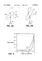
- FIG. 3Ais a schematic diagram illustrating the incident angle of the light of the system of FIG. 1 relative to a block of a transparent dielectric material useful for illustrating the invention.
- FIG. 3Bis a schematic diagram of the block of FIG. 3A, but where the incident angles of the laser light and its reflections relative to the block have been altered to improve the sensitivity of bright field detection to illustrate the preferred embodiment of the invention.
- FIG. 4is a graphical illustration of the reflectance of the block of transparent dielectric of FIG. 3B as a function of the angle of incidence to illustrate the preferred embodiment of the invention.
- FIG. 5is a schematic diagram illustrating a combined dark field and bright field system for detecting anomalies of a sample to illustrate an alternative embodiment of the invention.
- System 10 of FIG. 1is a laser-based scanner anomaly detection system to illustrate the preferred embodiment of the invention.
- the illumination system and the light collection and detection system of FIG. 1are stationary and the surface 12 of a sample to be inspected is moved along a spiral path.
- a spiral scan pathis accomplished by rotating the surface about a shaft or axle by a rotary motor, and simultaneously translating the shaft or axle along a line using a linear translation stage and motor combination.
- the rotational motion of the surface about the shaft or axle, and the translational motion of the shaft or axleare coordinated by controlling the two motors so that the illuminated portion of the surface traces a spiral path on the substrate.
- Surface 12is a light reflective surface, such as that of a semiconductor wafer, photomask, reticle, ceramic tile, or other surface.
- surface 12 to be inspectedis rotated about a shaft or axle 14 located behind the plane of the paper, so that the illumination portion of the system 10 causes two spots 16 and 18 of surface 12 to be illuminated.
- spots 16 and 18are located on a tangential path of the rotational motion of surface 12 about axle or shaft 14. If surface 12 is rotated about axle 14 along the direction of arrow 22 indicated, then the portion of the surface first illuminated within spot 16 will be illuminated in spot 18 at a later time.
- Surface 12is also moved relative to axle 14 in a translational motion so that spots 16, 18 will cover the entire surface 12 along a spiral path.
- System 10employs a bright field detection scheme that utilizes Nomarski's differential interference contrast principles.
- Nomarski's differential interference contrast principlesplease see “Quantitative Surface Topography Determination by Nomarski, Reflection Microscopy, I. Theory," by Delbert L. Lessor, John S. Hartman and Richard L. Gordon, Journal of Optical Society of America Vol. 69 No. 2, page 357 (1979).
- laser 30provides a coherent optical beam 32 substantially at a predetermined wavelength of linearly polarized light. Beam 32 is passed through a Faraday isolator 34 and a halfwave plate 36 and passes through a beam splitter 38 before it reaches a Wollaston prism 40.
- Beam splitter 38is of a type that preferably transmits 85% or more of the light in beam 32 towards the Wollaston prism.
- Halfwave plate 32is used to rotate the plane of polarization of beam 32 with respect to the vertical and horizontal axes of Wollaston prism 40 so that the beam 42 transmitted through beam splitter 38 is split into two beams 52 and 54, one with a vertical plane of polarization and the other with a horizontal plane of polarization.
- the beams 52 and 54are passed through the beam forming optics 42, reflected by mirror 44 through an aperture in an ellipsoidal container 46 towards another mirror 48 which reflects the two beams towards surface 12 to illuminate the two spots 16, 18 described above.
- beams 52, 54are substantially normal to surface 12
- the specular reflections of the two beams 52, 54 by surface 12substantially retrace the paths of the two incident beams, from surface 12 to mirror 48, mirror 44, beam forming optics 42, and are combined by Wollaston prism 40 into a single beam 56 again, with 85% or more of such combined beam passing through beam splitter 38 and then absorbed by Faraday isolator 34. But 15% or less of the light in such combined beam 56 is reflected by beam splitter 38 towards a bright field detector 60.
- A, Bare the complex electric fields of the reflections of respective beams 52, 54 by surface 12 in the combined beam 56, then the complex fields A, B are given by the equations below:
- ⁇is the angular optical frequency of laser 30 and .O slashed. 1 and .O slashed. 2 are the optical phases associated with or caused by surface 12 at spots 16, 18 respectively, and ⁇ 1 and ⁇ 2 are the average optical phases of two beams 52, 54 incident upon surface 12 and reflected therefrom, where the latter two terms ⁇ 1 , ⁇ 2 also include the effect of microphonics in the system such as temperature and pressure fluctuations and mechanical vibrations. In a differential interference contrast system such as system 10, however, due to the proximity of the two beams 52, 54 to each other, these spurious effects are almost identical and can be ignored.
- Polarizing beam splitter 62has its axes oriented at approximately 45° with respect to the axes of the Wollaston prism, so that the transmitted beam 72 and the reflected beam 74 have complex electric fields E 1 , E 2 given by the equations below: ##EQU1##
- Detector D1detects the intensity S 1 of beam 72 and detector D2 detects the intensity S 2 of beam 74, where S 1 , S 2 are proportional to quantities given below: ##EQU2##
- the quantity ⁇can be adjusted by adjusting the lateral incident position of the beam for illuminating the surface on Wollaston prism 40; preferably, such relative position is adjusted so that ⁇ has the value of 90° or ⁇ /2.
- the above equations for S 1 and S 2therefore reduce to the following: ##EQU3##
- phase difference ⁇ .O slashed.would be small, so that the above-described linearization process may be employed.
- Other schemes for linearizing the phase differencemay also be used, such as that described in "Linear Imaging in Scanning Polarization/Interference Contrast Microscopy," by C. W. See and M. Vaez-Iravani, Electronics Letters, Sep. 25, 1986, Vol. 22, No. 20, pages 1079-1081.
- the differential phase between the complex electric fields A, B of the reflections at spots 16, 18is measured by the difference output 66a, and is given by the quantity S in the equations above.
- system 10can be calibrated to measure the differential phase between the complex electric fields A, B.
- One important feature of system 10is the fact that, since the measured quantity S responds linearly to the differential phase between A, B, the measured quantity S preserves the sign of the differential phase; that is, whether the anomaly is a depression or an elevation on the surface 12. In this instance, a particle on the surface will give rise to a positive differential phase, just as with an elevation.
- the Wollaston-based system 10allows arbitrary phase biasing between the two beams 52, 54, which results in a guaranteed linear response of the system. Furthermore, since the system is differential in nature, it has major advantages in terms of the rejection of common mode noise, and cancellation of vibrations which are along the beam direction affecting the light paths of the two beams. In a normal mode of operation, the phase difference is obtained at a high frequency. This allows the possibility of applying a high pass filter to the output differential phase signal which, in turn, greatly alleviates complications due to vibration induced lateral shift of the Wollaston prism and the light beams passing through the prism.
- the total reflectance signal at output 66agives the total reflectance of a sample and can be used for normalizing the difference output signal at output 66a.
- the ellipsoidal collector 46reflects the scattered light from spots 16 and 18 towards a dark field detector 80.
- a dark field detector 80For a more detailed explanation of the operation of the ellipsoidal collector 46 and the dark field detector 80, please see U.S. patent application Ser. No. 08/216,834, filed Mar. 24, 1994, entitled “Process and Assembly for Non-destructive Testing of Surfaces," which is incorporated herein in its entirety by reference.
- Mirror 48prevents specular reflection from spots 16 and 18 from reaching the dark field detector 80.
- only the light rays collected by collector 46 from spot 16are shown in FIG. 1, it being understood that collector 46 will also collect light from spot 18 and direct such rays to detector 80.
- the separation between the spots 16, 18is exaggerated; such separation is typically half of a spot diameter or less.
- the phase detection scheme described above for bright field detectioncan differentiate between depression on the one hand and elevation or particle on the other; such bright field detection can be used to supplement dark field detection to yield more information on the surface anomaly. If a first laser is used to illuminate a first spot on the surface 12 for dark field detection and a second laser is used to illuminated a second spot on the surface 12 for bright field detection, then in order to benefit from both dark and bright field detections, one must be able to identify or register the dark field data for a particular spot on the surface with the bright field data for the same spot. This is cumbersome and any misregistration errors would defeat the purpose of using both bright and dark field detection.
- the scheme 10 of FIG. 1avoids this problem altogether since a single laser is used so that both the bright field detector 60 and the dark field detector 80 are detecting from surface features on the same area or areas such as spots 16, 18 on surface 12. This eliminates any need for methodology to remedy misalignment of bright and dark field data.
- the relative intensity of beams 52, 54may be such that one (e.g. beam 52) is at a much higher intensity than the other, such as where one beam is at an intensity that is twenty times or more that of the other.
- the optical arrangement for achieving such ratio of intensitiesis explained below. As shown below, the above advantages of a single laser for both bright and dark field detection can be retained without sacrificing significantly the illumination and hence the detection sensitivity of dark field detection. This is illustrated in FIG. 2.
- FIG. 2is a graphical plot of the point spread function of the two illuminated spots 16, 18 as seen by detector 80 where the intensity of the beam with a first polarization and having power P 1 illuminating one spot is twenty-four times the intensity of the other beam with a second different polarization and power P 2 illuminating the other spot.
- 102is the point spread function of the spot illuminated by the beam with the first polarization
- point spread function 104is that of the spot illuminated by the beam with the other polarization.
- the sum of the two functions as seen by detector 80is illustrated by curve 106.
- the combined point spread function of the two spots 16, 18is essentially the same as that of the spot 16 illuminated by the beam with the first polarization alone.
- the dark field detection system originally designed for detecting light scattered from a single illuminated spotneed not be altered to accommodate a combined dark and bright field detection system such as system 10 of FIG. 1.
- the halfwave plate 36is used to rotate the plane of polarization of beam 32 so that the plane of polarization is at such angle to the vertical and horizontal axes of the Wollaston prism 40 that beam 52 of the first polarization has an intensity or power P 1 that is at least twenty times the intensity or power P 2 of the other beam 54.
- the portion of the beam 58 from reflection of beam 52has P polarization and the portion of the beam 58 from the reflection of beam 54 has S polarization.
- Pis the total power of beam 56 before reflection by beam splitter 38
- P p and P sare respectively the powers of the P polarization and S polarization portions of beam 56 and ⁇ is the ratio P p /P
- the quantities P, P p , P sare related as follows:
- the intensity I out detected by detector D1 from beam 72is proportional to quantity given as follows: ##EQU4## where R p is the reflectance of the beam splitter 38 with respect to light of P polarization and R s is the reflectance of beam splitter 38 with respect to light of S polarization. If the beam splitter 38 has equal reflectance for light of P and S polarizations and if ⁇ is 24/25, then the intensity detected by detector D1 is given approximately as follows:
- Ris the reflectance of beam splitter 38 of light of both P and S polarizations.
- the phase shift that is detected by the bright field detector 60is reduced only by about 60% despite the big difference (24 to 1) in intensity between the light of P polarization and the light of S polarization in beam 58. If beam splitter 38 transmits 85% of incident light and reflects 15% of the incident light, then the total power P of beam 58 is about 12% of the light provided by laser 30, where this percentage may be further reduced due to the imperfect light reflection at the surface 12.
- One alternative scheme to the above described oneis to orient the halfwave plate 36 so that beams 52 and 54 have equal intensities; this would increase the percentage of laser power delivered to the bright field detector 60 at the cost of reducing the intensity density of light delivered to the dark field detector and hence its sensitivity. Even so, the total power of beam 58 sent to the bright field detector 60 would only be 25% of that of the light provided by laser 30 (again not taking into account the further reduction in intensity due to the imperfect light reflection at the surface 12), and such power is only about twice that delivered using the scheme described above in reference to FIG. 2. In other words, at a modest reduction (by a factor of about 2) of the total power delivered to the bright field detector 60, the intensity or power for dark field detection is not noticeably reduced so that the detection sensitivity of the dark field portion of the system is preserved.
- the scheme described aboveavoids a redesign of the dark field detection system at only a modest reduction in the total power of the light delivered to the bright field detector 60 and at a modest reduction of the phase shift signal detected by the detector 60.
- FIG. 3Ainstead of beam splitter 38, a block of a transparent dielectric material 138 is interposed between the halfwave plate 36 and the Wollaston prism 40.
- Block 138has two substantially parallel surfaces 138a, 138b.
- Block 138 in FIG. 3Ais oriented so that the surfaces 138a, 138b are at 45° to beams 32' and 56.
- FIG. 4is a graphical illustration of the reflectance of glass at different incidence angles of an incident beam of light, showing the reflectances of the light of both P and S polarizations.
- block 138has a higher reflectance of light of S polarization compared to that of P polarization except at very low and very high angles of incidence.
- the reflectance of light of S polarizationis roughly an order of magnitude higher than that for light of P polarization. This will tend to compensate for the reduction in signal of the phase shift detected by detector 60.
- Such range of angleshave values that are smaller than the Brewster angle of glass as shown below.
- the refractive index for glassis 1.5 so that the Brewster angle is about 56°. If a 64° incidence angle (greater than the Brewster angle) is chosen instead as illustrated in FIG. 3B, then the light reflectance of light of S polarization is about twenty to twenty-five times that of light of P polarization. In such event, the ratio R p /R s is approximately equal to (1- ⁇ )/ ⁇ , so that the intensity detected by detector D1 is proportional to a quantity given as follows: ##EQU5##
- the above-described reduction in the phase shift signal detected by detector 60is entirely compensated for, so that there is no longer such reduction.
- the value of the incidence anglemay be chosen from two ranges of values, with the values within one range less than and with values within the other range greater than the Brewster angle.
- the fringe visibility of detection 60can be derived and is given by the expression on the left hand side of the equation below.
- the fringe visibility of detection 60should be as high as possible, that is, as close to 1 as possible.
- nrefraction index of beam-splitter material.
- the choice of angle of incidence such as illustrated in FIGS. 3A, 3Bis such that fringe visibility is optimized.
- the above equations for the fringe visibilitymay be used to derive an optimum value for the incident angle between beams 32', 56 and the two surfaces 138a, 138b of block 138.
- FIG. 5a slightly modified scheme may be used for detecting anomalies on surfaces of or within layers of material that are transparent. This is illustrated in FIG. 5.
- the light transmitted towards spots 16, 18 on surface 12 of a layer of transparent material 200will pass through the surface and layer and be reflected by reflectors 152, 154 towards beam forming optics 156 and combined by a second Wollaston prism 160 (designed to be complementary with the first Wollaston prism 40) and directed to detector 60 to be detected in the same manner as described above. Since no reflected light will retrace the path of the incident beam towards the laser, no beam splitter will be necessary in the light path between laser 30 and surface 12.
Landscapes
- Physics & Mathematics (AREA)
- Health & Medical Sciences (AREA)
- Life Sciences & Earth Sciences (AREA)
- Chemical & Material Sciences (AREA)
- Analytical Chemistry (AREA)
- Biochemistry (AREA)
- General Health & Medical Sciences (AREA)
- General Physics & Mathematics (AREA)
- Immunology (AREA)
- Pathology (AREA)
- Investigating Materials By The Use Of Optical Means Adapted For Particular Applications (AREA)
- Testing Or Measuring Of Semiconductors Or The Like (AREA)
Abstract
Description
This invention relates in general to systems for detecting anomalies of samples, and in particular to a single laser bright field and dark field system for detecting anomalies on samples such as semiconductor wafers, photomasks, reticles and ceramic tiles.
The size of semiconductor devices fabricated on silicon wafers has been continually reduced. At the present time, for example, semiconductor devices can be fabricated at a resolution of a half micron or less, and 64 megabit DRAMS are being fabricated with a 0.35 micron design rule. The shrinking of semiconductor devices to smaller and smaller sizes has imposed a much more stringent requirement on the sensitivity of wafer inspection instruments which are called upon to detect contaminant particles and surface defects that are small compared to the size of the semiconductor devices. In addition to the detection of the presence of a defect, frequently it is useful also to know the structural characteristics of the defect, such as whether a surface defect is an elevation or a depression in the surface.
Many wafer inspection instruments are dark field systems, where light scattered on a surface is inspected to detect particles and surface defects. One of the problems in a dark field system is that, due to the fact that information concerning structural characteristics of the defects may be lost because of the scattering, it may be difficult or impossible for dark field systems to determine the structural characteristics of the defects, such as whether the defect is an elevation or a depression in the surface. While it is possible for bright field systems to detect the structural characteristics of the defect, the ever present background signal can be many orders of magnitude larger than the feature related signal from the defect.
Thus none of the conventional systems or systems proposed is entirely satisfactory. It is therefore desirable to provide an improved anomaly detection system which can detect anomalies which are small relative to the size of the semiconductor devices as well as the structural characteristics of the defects.
This invention is based on the observation that both dark field detection and bright field detection may be employed for detecting particles and surface defects that are small compared to the size of semiconductor devices as well as the structural characteristics of the defects. While two lasers may be used, one for the bright field portion and one for the dark field portion of the system, it is advantageous to use a single laser for both portions of the system in a manner that facilitates the registration of areas detected by the two portions of the system.
One aspect of the invention is directed towards a system for detecting anomalies of a sample, comprising means for transmitting to said sample two substantially parallel optical incident beams. The beams are initially coherent but are of different polarizations, so that any anomaly of the sample and illuminated by one of the beams causes a phase shift in a beam resulting from transmission or reflection of said one of the incident beams by the sample. The system further comprises at least one dark field detector detecting light scattered by the sample from the two incident beams and a bright field detector detecting any phase shift in transmissions or reflections of the two incident beams by the sample.
Another aspect of the invention is directed towards a method for detecting anomalies of a sample, comprising the steps of transmitting to said sample two substantially parallel optical incident beams, said beams being initially coherent but of different polarizations, so that any anomaly of said sample and illuminated by one of the beams causes a phase shift in a beam resulting from transmission or reflection of said one of the incident beams by the sample; detecting light scattered by the sample from the two incident beams; and detecting any phase shift in transmissions or reflections of the two incident beams by the sample.
FIG. 1 is a schematic diagram illustrating a combined dark field and bright field system for detecting anomalies on a surface to illustrate the preferred embodiment of the invention.
FIG. 2 is a graphical plot of the point spread function of the system of FIG. 1 to illustrate the preferred embodiment of the invention.
FIG. 3A is a schematic diagram illustrating the incident angle of the light of the system of FIG. 1 relative to a block of a transparent dielectric material useful for illustrating the invention.
FIG. 3B is a schematic diagram of the block of FIG. 3A, but where the incident angles of the laser light and its reflections relative to the block have been altered to improve the sensitivity of bright field detection to illustrate the preferred embodiment of the invention.
FIG. 4 is a graphical illustration of the reflectance of the block of transparent dielectric of FIG. 3B as a function of the angle of incidence to illustrate the preferred embodiment of the invention.
FIG. 5 is a schematic diagram illustrating a combined dark field and bright field system for detecting anomalies of a sample to illustrate an alternative embodiment of the invention.
For simplicity in description, identical components are identified by the same numerals in the application.
If A, B are the complex electric fields of the reflections ofrespective beams surface 12 in the combinedbeam 56, then the complex fields A, B are given by the equations below:
A=e.sub.1 r.sub.1 exp {j(ωt+.O slashed..sub.1 β.sub.1)}B=e.sub.2 r.sub.2 exp {j(ωt+.O slashed..sub.2 β.sub.2)}where e1, e2 are the amplitudes of the incident electric fields ofbeams spots laser 30 and .O slashed.1 and .O slashed.2 are the optical phases associated with or caused bysurface 12 atspots beams surface 12 and reflected therefrom, where the latter two terms β1, β2 also include the effect of microphonics in the system such as temperature and pressure fluctuations and mechanical vibrations. In a differential interference contrast system such assystem 10, however, due to the proximity of the twobeams
Polarizingbeam splitter 62 has its axes oriented at approximately 45° with respect to the axes of the Wollaston prism, so that the transmittedbeam 72 and thereflected beam 74 have complex electric fields E1, E2 given by the equations below: ##EQU1##
Detector D1 detects the intensity S1 ofbeam 72 and detector D2 detects the intensity S2 ofbeam 74, where S1, S2 are proportional to quantities given below: ##EQU2##
In a manner known to those skilled in the art, the quantity β can be adjusted by adjusting the lateral incident position of the beam for illuminating the surface on Wollastonprism 40; preferably, such relative position is adjusted so that β has the value of 90° or π/2. The above equations for S1 and S2 therefore reduce to the following: ##EQU3##
For most anomalies, the phase difference δ.O slashed. would be small, so that the above-described linearization process may be employed. Other schemes for linearizing the phase difference may also be used, such as that described in "Linear Imaging in Scanning Polarization/Interference Contrast Microscopy," by C. W. See and M. Vaez-Iravani, Electronics Letters, Sep. 25, 1986, Vol. 22, No. 20, pages 1079-1081.
Thus from the above equations, it is seen that the differential phase between the complex electric fields A, B of the reflections atspots difference output 66a, and is given by the quantity S in the equations above. Thussystem 10 can be calibrated to measure the differential phase between the complex electric fields A, B. One important feature ofsystem 10 is the fact that, since the measured quantity S responds linearly to the differential phase between A, B, the measured quantity S preserves the sign of the differential phase; that is, whether the anomaly is a depression or an elevation on thesurface 12. In this instance, a particle on the surface will give rise to a positive differential phase, just as with an elevation. An inherent feature of the Wollaston-basedsystem 10 is that it allows arbitrary phase biasing between the twobeams output 66a gives the total reflectance of a sample and can be used for normalizing the difference output signal atoutput 66a.
Theellipsoidal collector 46 reflects the scattered light fromspots dark field detector 80. For a more detailed explanation of the operation of theellipsoidal collector 46 and thedark field detector 80, please see U.S. patent application Ser. No. 08/216,834, filed Mar. 24, 1994, entitled "Process and Assembly for Non-destructive Testing of Surfaces," which is incorporated herein in its entirety by reference.Mirror 48 prevents specular reflection fromspots dark field detector 80. For simplicity, only the light rays collected bycollector 46 fromspot 16 are shown in FIG. 1, it being understood thatcollector 46 will also collect light fromspot 18 and direct such rays todetector 80. Also for clarity of illustration, the separation between thespots
While dark field detection can be very sensitive to small surface anomalies, dark field detection alone typically does not yield information on the structural characteristics of the surface anomaly. As noted above, the phase detection scheme described above for bright field detection can differentiate between depression on the one hand and elevation or particle on the other; such bright field detection can be used to supplement dark field detection to yield more information on the surface anomaly. If a first laser is used to illuminate a first spot on thesurface 12 for dark field detection and a second laser is used to illuminated a second spot on thesurface 12 for bright field detection, then in order to benefit from both dark and bright field detections, one must be able to identify or register the dark field data for a particular spot on the surface with the bright field data for the same spot. This is cumbersome and any misregistration errors would defeat the purpose of using both bright and dark field detection.
Thescheme 10 of FIG. 1 avoids this problem altogether since a single laser is used so that both thebright field detector 60 and thedark field detector 80 are detecting from surface features on the same area or areas such asspots surface 12. This eliminates any need for methodology to remedy misalignment of bright and dark field data.
To avoid reducing significantly the intensity of illumination and hence the detection sensitivity in dark field detection systems, the relative intensity ofbeams
Many dark field detection systems have been designed assuming that only a single spot of the surface to be inspected is to be illuminated at any one time so that data processing is performed assuming the point spread function of a single spot. Therefore, the presence of twodifferent spots surface 12, and is undesirable. The present invention eliminates the need for such redesign as explained below.
FIG. 2 is a graphical plot of the point spread function of the two illuminatedspots detector 80 where the intensity of the beam with a first polarization and having power P1 illuminating one spot is twenty-four times the intensity of the other beam with a second different polarization and power P2 illuminating the other spot. As shown in FIG. 2, 102 is the point spread function of the spot illuminated by the beam with the first polarization andpoint spread function 104 is that of the spot illuminated by the beam with the other polarization. The sum of the two functions as seen bydetector 80 is illustrated bycurve 106. As is clear from FIG. 2, the combined point spread function of the twospots spot 16 illuminated by the beam with the first polarization alone. Hence the dark field detection system originally designed for detecting light scattered from a single illuminated spot need not be altered to accommodate a combined dark and bright field detection system such assystem 10 of FIG. 1.
Thehalfwave plate 36 is used to rotate the plane of polarization ofbeam 32 so that the plane of polarization is at such angle to the vertical and horizontal axes of theWollaston prism 40 thatbeam 52 of the first polarization has an intensity or power P1 that is at least twenty times the intensity or power P2 of theother beam 54.
The operation of thebright field detector 60 will now be described. Upon reflection bybeam splitter 38, the portion of thebeam 58 from reflection ofbeam 52 has P polarization and the portion of thebeam 58 from the reflection ofbeam 54 has S polarization. Assuming that P is the total power ofbeam 56 before reflection bybeam splitter 38, Pp and Ps are respectively the powers of the P polarization and S polarization portions ofbeam 56 and γ is the ratio Pp /P, then the quantities P, Pp, Ps are related as follows:
P.sub.p =Pγ and P.sub.s =P(1-y)
Then the intensity Iout detected by detector D1 frombeam 72 is proportional to quantity given as follows: ##EQU4## where Rp is the reflectance of thebeam splitter 38 with respect to light of P polarization and Rs is the reflectance ofbeam splitter 38 with respect to light of S polarization. If thebeam splitter 38 has equal reflectance for light of P and S polarizations and if γ is 24/25, then the intensity detected by detector D1 is given approximately as follows:
I.sub.out αPR(1-2/5δ.O slashed.)
where R is the reflectance ofbeam splitter 38 of light of both P and S polarizations.
In other words, ifbeam splitter 38 has the same reflectance irrespective of polarization, and where light of P polarization is of an intensity twenty-four times that of the S polarization, the phase shift that is detected by thebright field detector 60 is reduced only by about 60% despite the big difference (24 to 1) in intensity between the light of P polarization and the light of S polarization inbeam 58. Ifbeam splitter 38 transmits 85% of incident light and reflects 15% of the incident light, then the total power P ofbeam 58 is about 12% of the light provided bylaser 30, where this percentage may be further reduced due to the imperfect light reflection at thesurface 12.
One alternative scheme to the above described one is to orient thehalfwave plate 36 so thatbeams bright field detector 60 at the cost of reducing the intensity density of light delivered to the dark field detector and hence its sensitivity. Even so, the total power ofbeam 58 sent to thebright field detector 60 would only be 25% of that of the light provided by laser 30 (again not taking into account the further reduction in intensity due to the imperfect light reflection at the surface 12), and such power is only about twice that delivered using the scheme described above in reference to FIG. 2. In other words, at a modest reduction (by a factor of about 2) of the total power delivered to thebright field detector 60, the intensity or power for dark field detection is not noticeably reduced so that the detection sensitivity of the dark field portion of the system is preserved.
As noted above, where beams 52, 54 have the same intensity, this will require the data processing portion of the dark field detection system be altered to accommodate detection from two illuminated spots, which is undesirable. In other words, the scheme described above avoids a redesign of the dark field detection system at only a modest reduction in the total power of the light delivered to thebright field detector 60 and at a modest reduction of the phase shift signal detected by thedetector 60.
The above-described 60% reduction in the phase shift signal can be compensated for by using a transparent dielectric material instead of abeam splitter 38 as described below in reference to FIGS. 3A, 3B and 4. As shown in FIG. 3A, instead ofbeam splitter 38, a block of a transparentdielectric material 138 is interposed between thehalfwave plate 36 and theWollaston prism 40.Block 138 has two substantiallyparallel surfaces Block 138 in FIG. 3A is oriented so that thesurfaces beams 32' and 56. FIG. 4 is a graphical illustration of the reflectance of glass at different incidence angles of an incident beam of light, showing the reflectances of the light of both P and S polarizations. As is evident from FIG. 4, ifblock 138 is made of glass, it has a higher reflectance of light of S polarization compared to that of P polarization except at very low and very high angles of incidence. At 45° angle of incidence as shown in FIG. 3A, the reflectance of light of S polarization is roughly an order of magnitude higher than that for light of P polarization. This will tend to compensate for the reduction in signal of the phase shift detected bydetector 60. There is a range of angles around 45 degrees within which the relative reflectances of light of P and S polarizations will compensate for the reduction in signal of the phase shift detected bydetector 60. Such range of angles have values that are smaller than the Brewster angle of glass as shown below. Thus if the incidence angle is chosen to be within such range, the reduction in the phase shift signal due to the disparity in intensities ofbeams
In reference to FIG. 4, the refractive index for glass is 1.5 so that the Brewster angle is about 56°. If a 64° incidence angle (greater than the Brewster angle) is chosen instead as illustrated in FIG. 3B, then the light reflectance of light of S polarization is about twenty to twenty-five times that of light of P polarization. In such event, the ratio Rp /Rs is approximately equal to (1-γ)/γ, so that the intensity detected by detector D1 is proportional to a quantity given as follows: ##EQU5##
In other words, by using a transparent dielectric having a reflectance ratio Rp /Rs that compensates for the big difference in intensity between thebeams detector 60 is entirely compensated for, so that there is no longer such reduction. Again there is a range of angles around 64 degrees within which the relative reflectances of light of P and S polarizations will compensate for the reduction in signal of the phase shift detected bydetector 60. In general, to compensate for the reduction in the phase shift signal, the value of the incidence angle may be chosen from two ranges of values, with the values within one range less than and with values within the other range greater than the Brewster angle.
From the equations above, the fringe visibility ofdetection 60 can be derived and is given by the expression on the left hand side of the equation below. For best results, the fringe visibility ofdetection 60 should be as high as possible, that is, as close to 1 as possible. For a practical system, it is assumed that the fringe visibility ofdetection 60 is greater than 0.9, as given by the equation below: ##EQU6## with θ=angle of incidence θ'=angle of refraction=sin-1 (1/n)sin(θ)!
n=refraction index of beam-splitter material.
Note that if other values of fringe visibility are acceptable, then one simply changes 0.9 to one of those values.
Preferably, the choice of angle of incidence such as illustrated in FIGS. 3A, 3B is such that fringe visibility is optimized. Once a suitable material has been selected for the transparent dielectric inblock 138 so that its refractive index is known, then the above equations for the fringe visibility may be used to derive an optimum value for the incident angle betweenbeams 32', 56 and the twosurfaces block 138.
While the invention has been described above by reference to detection of light reflected from anopaque surface 12 such as that of a semiconductor wafer, a slightly modified scheme may be used for detecting anomalies on surfaces of or within layers of material that are transparent. This is illustrated in FIG. 5. As shown in FIG. 5, the light transmitted towardsspots surface 12 of a layer oftransparent material 200 will pass through the surface and layer and be reflected byreflectors beam forming optics 156 and combined by a second Wollaston prism 160 (designed to be complementary with the first Wollaston prism 40) and directed todetector 60 to be detected in the same manner as described above. Since no reflected light will retrace the path of the incident beam towards the laser, no beam splitter will be necessary in the light path betweenlaser 30 andsurface 12.
While the invention has been described above by reference to various embodiments, it will be understood that different changes and modifications may be made without departing from the scope of the invention which is to be limited only by the appended claims.
Claims (16)
1. A system for detecting anomalies of a sample, comprising:
means for transmitting to said sample two substantially parallel optical incident beams, said beams being initially coherent but of different polarizations, so that portions of the beams are reflected or transmitted by the sample;
at least one dark field detector detecting intensity of light scattered by the sample from the two incident beams; and
a bright field detector detecting any phase shift between the reflected or transmitted portions of the two incident beams.
2. The system of claim 1, further comprising means for combining the reflected or transmitted portions of the two beams to form a combined beam; wherein said bright field detector includes:
means for separating the combined beam or a beam obtained therefrom into a first and a second output beam having different polarizations; and
means for detecting the first and second output beams to provide two outputs and for subtracting the two outputs to provide a phase shift signal.
3. The system of claim 1, wherein one of the two incident beams is at a higher intensity than the other of the two incident beams.
4. The system of claim 3, wherein one of the two incident beams is at an intensity at least 20 times that of the other of the two incident beams.
5. The system of claim 1, said transmitting means including:
a laser to provide a coherent light beam towards the sample;
a beam splitter passing the coherent light beam from the laser towards the sample, and reflecting reflections by the sample of such beam towards the bright field detector, wherein the beam splitter passes 85% or more of the light incident on it.
6. The system of claim 1, said transmitting means including a body of a transparent dielectric material.
7. The system of claim 6, wherein said transmitting means includes means for providing a laser beam, said dielectric material having a Brewster angle, said body being in the shape of a block with an incident surface and a reflecting surface, said two surfaces substantially parallel to one another, said beam provided by the laser being directed towards the incident surface at an incident angle which has a value in one of two ranges, the values of one of said two ranges being greater than and the values of the other of said two ranges being smaller than the Brewster angle of the dielectric material.
8. The system of claim 1, said two incident beams simultaneously illuminating at least two areas of the sample, wherein the at least one dark field detector detects light scattered by the simultaneously illuminated areas of the sample and the bright field detector detects the reflected or transmitted portions of the two beams from the simultaneously illuminated areas of the sample.
9. A method for detecting anomalies of a sample, comprising the steps of
transmitting to said sample two substantially parallel optical incident beams, said beams being initially coherent but of different polarizations, so that portions of the beams are reflected or transmitted by the sample;
detecting light scattered by the sample from the two incident beams without substantially detecting light directly from the incident beams and the reflected or transmitted portions; and
detecting any phase shift between the reflected or transmitted portions of the two incident beams.
10. The method of claim 9, further comprising combining the reflected or transmitted portions of the two beams by the sample to form a combined beam; wherein said phase shift detecting step includes:
separating the combined beam or a beam obtained therefrom into a first and a second output beam having different polarizations; and
detecting the first and second output beams to provide two outputs and for subtracting the two outputs to provide a phase shift signal.
11. The method of claim 9, wherein one of the two incident beams is at a higher intensity than the other of the two incident beams.
12. The method of claim 11, wherein one of the two incident beams is at an intensity at least 20 times that of the other of the two incident beams.
13. The method of claim 9, said transmitting step including:
directing a coherent light beam towards the sample;
providing a beam splitter passing the coherent beam from the laser towards the sample, and reflecting reflections from the sample of such beam towards the bright field detector, wherein the beam splitter passes 85% or more of the light incident on it.
14. The method of claim 13, wherein said transmitting step includes providing a body of a transparent dielectric material for passing the coherent beam towards the sample and reflecting reflections by the sample towards a bright field detector, said body being in the shape of a block with an incident surface and a reflecting surface, said two surfaces being substantially parallel to one another, said transmitting step including directing the coherent beam towards the incident surface at an incident angle.
15. The method of claim 14, further comprising the step of determining, prior to the directing step, an optimal value for the incident angle as a function of the index of refraction of the dielectric material, and of a desired fringe visibility.
16. The method of claim 9, said transmitting step causing the two incident beams to simultaneously illuminate at least two areas of the sample, wherein the two detecting steps detect light scattered by and phase shift between the transmitted portions or reflected portions from the simultaneously illuminated areas of the sample.
Priority Applications (4)
| Application Number | Priority Date | Filing Date | Title |
|---|---|---|---|
| US08/611,109US5798829A (en) | 1996-03-05 | 1996-03-05 | Single laser bright field and dark field system for detecting anomalies of a sample |
| AU22132/97AAU2213297A (en) | 1996-03-05 | 1997-03-05 | Single laser bright field and dark field system for detecting anomalies of a sample |
| PCT/US1997/004134WO1997033158A1 (en) | 1996-03-05 | 1997-03-05 | Single laser bright field and dark field system for detecting anomalies of a sample |
| JP53204397AJP3955329B2 (en) | 1996-03-05 | 1997-03-05 | Single laser brightfield and darkfield apparatus for detecting sample anomalies |
Applications Claiming Priority (1)
| Application Number | Priority Date | Filing Date | Title |
|---|---|---|---|
| US08/611,109US5798829A (en) | 1996-03-05 | 1996-03-05 | Single laser bright field and dark field system for detecting anomalies of a sample |
Publications (1)
| Publication Number | Publication Date |
|---|---|
| US5798829Atrue US5798829A (en) | 1998-08-25 |
Family
ID=24447663
Family Applications (1)
| Application Number | Title | Priority Date | Filing Date |
|---|---|---|---|
| US08/611,109Expired - LifetimeUS5798829A (en) | 1996-03-05 | 1996-03-05 | Single laser bright field and dark field system for detecting anomalies of a sample |
Country Status (4)
| Country | Link |
|---|---|
| US (1) | US5798829A (en) |
| JP (1) | JP3955329B2 (en) |
| AU (1) | AU2213297A (en) |
| WO (1) | WO1997033158A1 (en) |
Cited By (115)
| Publication number | Priority date | Publication date | Assignee | Title |
|---|---|---|---|---|
| WO1999014575A1 (en)* | 1997-09-19 | 1999-03-25 | Kla-Tencor Corporation | Improved sample inspection system |
| US6118525A (en)* | 1995-03-06 | 2000-09-12 | Ade Optical Systems Corporation | Wafer inspection system for distinguishing pits and particles |
| WO2000029807A3 (en)* | 1998-11-18 | 2000-11-23 | Kla Tencor Corp | Detection system for nanometer scale topographic measurements of reflective surfaces |
| US6153873A (en)* | 1998-05-20 | 2000-11-28 | E. I. Dupont De Numours And Company | Optical probe having an imaging apparatus |
| US20020015146A1 (en)* | 1997-09-22 | 2002-02-07 | Meeks Steven W. | Combined high speed optical profilometer and ellipsometer |
| US20020041374A1 (en)* | 2000-10-10 | 2002-04-11 | Yoshimasa Ohshima | Apparatus for detecting foreign particle and defect and the same method |
| US20020145740A1 (en)* | 2001-03-26 | 2002-10-10 | Meeks Steven W. | Material independent optical profilometer |
| WO2002082064A1 (en)* | 2001-04-06 | 2002-10-17 | Kla-Tencor Corporation | Improved defect detection system |
| US20020163634A1 (en)* | 2001-03-26 | 2002-11-07 | Meeks Steven W. | Multiple spot size optical profilometer, ellipsometer, reflectometer and scatterometer |
| US6486946B1 (en) | 1999-06-15 | 2002-11-26 | Ade Corporation | Method for discriminating between holes in and particles on a film covering a substrate |
| US20020186368A1 (en)* | 2001-06-08 | 2002-12-12 | Eliezer Rosengaus | Systems and methods for inspection of specimen surfaces |
| US20030025905A1 (en)* | 2001-03-26 | 2003-02-06 | Meeks Steven W. | Method of detecting and classifying scratches, particles and pits on thin film disks or wafers |
| US6538730B2 (en)* | 2001-04-06 | 2003-03-25 | Kla-Tencor Technologies Corporation | Defect detection system |
| US20030139838A1 (en)* | 2002-01-16 | 2003-07-24 | Marella Paul Frank | Systems and methods for closed loop defect reduction |
| US6633831B2 (en) | 2000-09-20 | 2003-10-14 | Kla Tencor Technologies | Methods and systems for determining a critical dimension and a thin film characteristic of a specimen |
| US20030197874A1 (en)* | 2002-04-19 | 2003-10-23 | Moghaddam Alireza Shahdoost | Method of detecting the thickness of thin film disks or wafers |
| US6673637B2 (en) | 2000-09-20 | 2004-01-06 | Kla-Tencor Technologies | Methods and systems for determining a presence of macro defects and overlay of a specimen |
| US20040017561A1 (en)* | 1997-09-22 | 2004-01-29 | Meeks Steven W. | Method of detecting and classifying scratches and particles on thin film disks or wafers |
| US6694284B1 (en) | 2000-09-20 | 2004-02-17 | Kla-Tencor Technologies Corp. | Methods and systems for determining at least four properties of a specimen |
| US20040032581A1 (en)* | 2002-01-15 | 2004-02-19 | Mehrdad Nikoonahad | Systems and methods for inspection of specimen surfaces |
| US6696362B2 (en)* | 2001-02-08 | 2004-02-24 | Applied Materials Inc. | Method for using an in situ particle sensor for monitoring particle performance in plasma deposition processes |
| US20040046959A1 (en)* | 1997-09-22 | 2004-03-11 | Meeks Steven W. | System and method for simultaneously measuring thin film layer thickness, reflectivity, roughness, surface profile and magnetic pattern on thin film magnetic disks and silicon wafers |
| US6717671B1 (en) | 1997-09-22 | 2004-04-06 | Candela Instruments | System for simultaneously measuring thin film layer thickness, reflectivity, roughness, surface profile and magnetic pattern |
| US20040095573A1 (en)* | 2000-09-12 | 2004-05-20 | Tsai Bin-Ming Benjamin | Excimer laser inspection system |
| US6757056B1 (en) | 2001-03-26 | 2004-06-29 | Candela Instruments | Combined high speed optical profilometer and ellipsometer |
| US20040125368A1 (en)* | 2002-09-13 | 2004-07-01 | Mehdi Vaez-Iravani | Inspection system for integrated applications |
| US20040136665A1 (en)* | 2003-01-15 | 2004-07-15 | Negevtech Ltd. | Fiber optical illumination system |
| US20040146295A1 (en)* | 2003-01-15 | 2004-07-29 | Negevtech Ltd. | System for detection of wafer defects |
| US20040156043A1 (en)* | 2003-01-09 | 2004-08-12 | Orbotech Ltd | Method and apparatus for simultaneous 2-D and topographical inspection |
| US6782337B2 (en) | 2000-09-20 | 2004-08-24 | Kla-Tencor Technologies Corp. | Methods and systems for determining a critical dimension an a presence of defects on a specimen |
| US20040169850A1 (en)* | 1999-07-02 | 2004-09-02 | Meeks Steven W. | System and method for double sided optical inspection of thin film disks or wafers |
| US6812045B1 (en) | 2000-09-20 | 2004-11-02 | Kla-Tencor, Inc. | Methods and systems for determining a characteristic of a specimen prior to, during, or subsequent to ion implantation |
| US6853446B1 (en) | 1999-08-16 | 2005-02-08 | Applied Materials, Inc. | Variable angle illumination wafer inspection system |
| US20050094864A1 (en)* | 2003-10-29 | 2005-05-05 | Xu James J. | Surface inspection system |
| US20050094136A1 (en)* | 2003-10-29 | 2005-05-05 | Xu James J. | Defect review system and method |
| US6891627B1 (en) | 2000-09-20 | 2005-05-10 | Kla-Tencor Technologies Corp. | Methods and systems for determining a critical dimension and overlay of a specimen |
| US20050099621A1 (en)* | 1997-09-19 | 2005-05-12 | Mehdi Vaez-Iravani | Sample inspection system |
| US20050105791A1 (en)* | 2003-10-29 | 2005-05-19 | Lee Ken K. | Surface inspection method |
| US6898037B2 (en) | 2001-02-20 | 2005-05-24 | Seagate Technology Llc | Optical equipment assemblies and techniques |
| US20050134841A1 (en)* | 1998-09-18 | 2005-06-23 | Mehdi Vacz-Iravani | Sample inspection system |
| US6919957B2 (en) | 2000-09-20 | 2005-07-19 | Kla-Tencor Technologies Corp. | Methods and systems for determining a critical dimension, a presence of defects, and a thin film characteristic of a specimen |
| US6956644B2 (en) | 1997-09-19 | 2005-10-18 | Kla-Tencor Technologies Corporation | Systems and methods for a wafer inspection system using multiple angles and multiple wavelength illumination |
| US20050254065A1 (en)* | 2004-05-12 | 2005-11-17 | Stokowski Stanley E | Method and apparatus for detecting surface characteristics on a mask blank |
| US20060007434A1 (en)* | 2004-07-12 | 2006-01-12 | Dov Furman | Multi mode inspection method and apparatus |
| US20060012781A1 (en)* | 2004-07-14 | 2006-01-19 | Negevtech Ltd. | Programmable spatial filter for wafer inspection |
| US20060068512A1 (en)* | 2004-09-29 | 2006-03-30 | Yoshimasa Ohshima | Method and apparatus for detecting defects |
| US20060087742A1 (en)* | 2004-10-26 | 2006-04-27 | Seiko Epson Corporation | Method of manufacturing a microlens substrate, a substrate with concave portions, a microlens substrate, a transmission screen, and a rear projection |
| US20060139629A1 (en)* | 2004-12-09 | 2006-06-29 | Yoshimasa Ohshima | Method and apparatus for detecting defects |
| US7075741B1 (en) | 2004-06-14 | 2006-07-11 | Kla Tencor Technologues Corporation | System and method for automatically determining magnetic eccentricity of a disk |
| US20060193507A1 (en)* | 2005-02-28 | 2006-08-31 | Negevtech Ltd. | Method and apparatus for detecting defects in wafers |
| US20060193506A1 (en)* | 2005-02-28 | 2006-08-31 | Negevtech Ltd. | Method and apparatus for detecting defects in wafers including alignment of the wafer images so as to induce the same smear in all images |
| US7106425B1 (en) | 2000-09-20 | 2006-09-12 | Kla-Tencor Technologies Corp. | Methods and systems for determining a presence of defects and a thin film characteristic of a specimen |
| US20060215289A1 (en)* | 2004-06-14 | 2006-09-28 | Kla-Tencor Technologies Corp. | Servo pattern characterization on magnetic disks |
| US7130029B2 (en) | 2000-09-20 | 2006-10-31 | Kla-Tencor Technologies Corp. | Methods and systems for determining an adhesion characteristic and a thickness of a specimen |
| US20060250609A1 (en)* | 2005-05-06 | 2006-11-09 | Kla-Tencor Technologies Corp. | Wafer edge inspection |
| US20060250611A1 (en)* | 2005-05-06 | 2006-11-09 | Kla-Tencor Technologies Corp. | Wafer edge inspection |
| US20060250612A1 (en)* | 1997-09-22 | 2006-11-09 | Meeks Steven W | Detecting and classifying surface features or defects by controlling the angle of the illumination plane of incidence with respect to the feature or defect |
| US20060256325A1 (en)* | 2005-05-11 | 2006-11-16 | Kla-Tencor Technologies Corp. | Illumination energy management in surface inspection |
| US20060256345A1 (en)* | 2005-05-12 | 2006-11-16 | Kla-Tencor Technologies Corp. | Interferometry measurement in disturbed environments |
| US20060262291A1 (en)* | 2005-05-17 | 2006-11-23 | Hess Harald F | Dynamic reference plane compensation |
| US20060268265A1 (en)* | 2005-05-31 | 2006-11-30 | Chuang Yung-Ho | Reducing variations in energy reflected from a sample due to thin film interference |
| US7201799B1 (en) | 2004-11-24 | 2007-04-10 | Kla-Tencor Technologies Corporation | System and method for classifying, detecting, and counting micropipes |
| US20070081151A1 (en)* | 2005-10-06 | 2007-04-12 | David Shortt | Methods and systems for inspection of a wafer |
| US20070103676A1 (en)* | 1994-03-24 | 2007-05-10 | Kla-Tencor Corporation | Process and Assembly for Non-Destructive Surface Inspections |
| US20070117225A1 (en)* | 2005-11-21 | 2007-05-24 | Capaldo Kevin P | Integrated inspection system and defect correction method |
| US20070114693A1 (en)* | 2005-11-21 | 2007-05-24 | Buckley Paul W | Methods for improving mold quality for use in the manufacture of liquid crystal display components |
| US20070116350A1 (en)* | 2005-11-21 | 2007-05-24 | Cheverton Mark A | Method for detecting the alignment of films for automated defect detection |
| US20070115460A1 (en)* | 2005-11-21 | 2007-05-24 | Capaldo Kevin P | Method for examining molds and apparatus for accomplishing the same |
| US20070115483A1 (en)* | 1997-09-22 | 2007-05-24 | Oak Dave S | Surface finish roughness measurement |
| US20070115464A1 (en)* | 2005-11-21 | 2007-05-24 | Harding Kevin G | System and method for inspection of films |
| US20070146694A1 (en)* | 2003-01-15 | 2007-06-28 | Negevtech Ltd. | Fiber optical illumination system |
| US7286229B1 (en) | 2005-09-06 | 2007-10-23 | Kla-Tencor Technologies Corporation | Detecting multi-domain states in perpendicular magnetic media |
| US20070252976A1 (en)* | 2006-04-26 | 2007-11-01 | Siemens Aktiengesellschaft | Optical sensor and method for optically inspecting surfaces |
| US7295300B1 (en) | 2005-09-28 | 2007-11-13 | Kla-Tencor Technologies Corporation | Detecting surface pits |
| US20070262771A1 (en)* | 2006-05-11 | 2007-11-15 | Kla-Tencor Technologies Corporation | Method and System for Perpendicular Magnetic Media Metrology |
| US20070268484A1 (en)* | 2006-05-17 | 2007-11-22 | Hitachi High Technologies Corp. | Optical inspection method and optical inspection apparatus |
| US20080002194A1 (en)* | 2006-06-30 | 2008-01-03 | Shigeru Matsui | Optical inspection method and optical inspection apparatus |
| US20080007725A1 (en)* | 2006-07-07 | 2008-01-10 | Hitachi High-Technologies Corporation | Method for detecting particles and defects and inspection equipment thereof |
| US20080013076A1 (en)* | 2006-07-13 | 2008-01-17 | Hitachi High-Technologies Corporation | Surface Inspection Method and Surface Inspection Apparatus |
| US20080013084A1 (en)* | 2006-07-13 | 2008-01-17 | Hitachi High-Technologies Corporation | Surface Inspection Method and Surface Inspection Apparatus |
| US20080015810A1 (en)* | 2006-07-12 | 2008-01-17 | Hitachi High-Technologies Corporation | Surface inspection method and surface inspection apparatus |
| US7349090B2 (en) | 2000-09-20 | 2008-03-25 | Kla-Tencor Technologies Corp. | Methods and systems for determining a property of a specimen prior to, during, or subsequent to lithography |
| US20080123434A1 (en)* | 2006-06-26 | 2008-05-29 | Masao Kuriyama | Erase discharge control method of nonvolatile semiconductor memory device |
| US20080137073A1 (en)* | 2006-11-28 | 2008-06-12 | Negevtech, Ltd. | Image Splitting in Optical Inspection Systems |
| US20080137074A1 (en)* | 2006-11-28 | 2008-06-12 | Negevtech, Ltd. | Image Splitting in Optical Inspection Systems |
| US7397553B1 (en) | 2005-10-24 | 2008-07-08 | Kla-Tencor Technologies Corporation | Surface scanning |
| US7396022B1 (en) | 2004-09-28 | 2008-07-08 | Kla-Tencor Technologies Corp. | System and method for optimizing wafer flatness at high rotational speeds |
| US20080174764A1 (en)* | 2006-09-01 | 2008-07-24 | Hitachi High-Technologies Corporation | Surface Inspection Method and Surface Inspection Apparatus |
| US20080180656A1 (en)* | 2007-01-26 | 2008-07-31 | Kla-Tencor Technologies Corporation | Surface characteristic analysis |
| US7433034B1 (en) | 2005-06-17 | 2008-10-07 | Nanometrics Incorporated | Darkfield defect inspection with spectral contents |
| US7463349B1 (en) | 2006-06-02 | 2008-12-09 | Kla-Tencor Technologies Corp. | Systems and methods for determining a characteristic of a specimen |
| US20090009753A1 (en)* | 2007-07-04 | 2009-01-08 | Hitachi High-Technologies Corporation | Inspection method and inspection device |
| US20090040525A1 (en)* | 2007-08-10 | 2009-02-12 | Azmi Kadkly | Systems configured to inspect a wafer |
| US20090059236A1 (en)* | 2007-08-30 | 2009-03-05 | Kla-Tencor Technologies Corporation | Wafer Edge Inspection |
| US20090066940A1 (en)* | 2007-09-11 | 2009-03-12 | Hitachi High-Technologies Corporation | Surface inspection method and surface inspection apparatus |
| US20090161096A1 (en)* | 2002-04-18 | 2009-06-25 | Kla- Tencor Technologies Corporation | Simultaneous Multi-Spot Inspection And Imaging |
| US20090213364A1 (en)* | 2008-02-27 | 2009-08-27 | Hitachi High-Technologies Corporation | Surface inspection method and inspection device using the same |
| US7623229B1 (en) | 2008-10-07 | 2009-11-24 | Kla-Tencor Corporation | Systems and methods for inspecting wafers |
| US7684032B1 (en) | 2005-01-06 | 2010-03-23 | Kla-Tencor Corporation | Multi-wavelength system and method for detecting epitaxial layer defects |
| US20100073665A1 (en)* | 2008-02-05 | 2010-03-25 | Kla-Tencor Corporation | Defect detection using time delay lock-in thermography (lit) and dark field lit |
| US7714995B2 (en) | 1997-09-22 | 2010-05-11 | Kla-Tencor Corporation | Material independent profiler |
| US20100225903A1 (en)* | 2007-05-02 | 2010-09-09 | Hitachi High-Technologies Corporation | Pattern defect inspection apparatus and method |
| US20110134418A1 (en)* | 2008-08-08 | 2011-06-09 | Shigeru Matsui | Light source device, surface inspecting apparatus using the device, and method for calibrating surface inspecting apparatus using the device |
| US8031931B2 (en) | 2006-04-24 | 2011-10-04 | Applied Materials South East Asia Pte. Ltd. | Printed fourier filtering in optical inspection tools |
| US20120081701A1 (en)* | 2010-09-30 | 2012-04-05 | Hitachi High-Technologies Corporation | Method and apparatus for inspecting a surface of a substrate |
| US20140176943A1 (en)* | 2007-04-25 | 2014-06-26 | Hitachi High-Technologies Corporation | Surface defect inspection method and apparatus |
| US8823935B1 (en) | 2008-09-10 | 2014-09-02 | Kla-Tencor Corporation | Detecting and classifying surface defects with multiple radiation collectors |
| CN105210233A (en)* | 2013-02-28 | 2015-12-30 | 摩巴尔萨特有限公司 | Antenna for receiving and/or transmitting polarized communication signals |
| US20160202177A1 (en)* | 2015-01-12 | 2016-07-14 | Kla-Tencor Corporation | System and method for semiconductor wafer inspection and metrology |
| US9726615B2 (en) | 2014-07-22 | 2017-08-08 | Kla-Tencor Corporation | System and method for simultaneous dark field and phase contrast inspection |
| US10133188B2 (en) | 2015-12-23 | 2018-11-20 | Asml Netherlands B.V. | Metrology method, target and substrate |
| CN113508286A (en)* | 2019-03-21 | 2021-10-15 | 贝克顿·迪金森公司 | Light detection system and method of use |
| US11175220B2 (en) | 2019-07-08 | 2021-11-16 | Shanghai Institute Of Optics And Fine Mechanics, Chinese Academy Of Sciences | Surface defect measuring apparatus and method by microscopic scattering polarization imaging |
| US12175654B2 (en) | 2020-11-06 | 2024-12-24 | Carl Zeiss Metrology Llc | Surface inspection system and method for differentiating particulate contamination from defects on a surface of a specimen |
| US12422347B2 (en) | 2018-04-17 | 2025-09-23 | Chemometec A/S | Depicting of objects |
Families Citing this family (3)
| Publication number | Priority date | Publication date | Assignee | Title |
|---|---|---|---|---|
| US6407373B1 (en) | 1999-06-15 | 2002-06-18 | Applied Materials, Inc. | Apparatus and method for reviewing defects on an object |
| RU2184365C2 (en)* | 2000-08-21 | 2002-06-27 | Лысенко Галина Артуровна | Method for measuring phase shift of transparent optical anisotropic specimen |
| US6831742B1 (en) | 2000-10-23 | 2004-12-14 | Applied Materials, Inc | Monitoring substrate processing using reflected radiation |
Citations (13)
| Publication number | Priority date | Publication date | Assignee | Title |
|---|---|---|---|---|
| US4353650A (en)* | 1980-06-16 | 1982-10-12 | The United States Of America As Represented By The United States Department Of Energy | Laser heterodyne surface profiler |
| US4449818A (en)* | 1981-02-10 | 1984-05-22 | Hitachi Metals, Ltd. | Method of inspecting microscopic surface defects |
| US4595289A (en)* | 1984-01-25 | 1986-06-17 | At&T Bell Laboratories | Inspection system utilizing dark-field illumination |
| JPS61198008A (en)* | 1985-02-28 | 1986-09-02 | Fujitsu Ltd | image detection device |
| US4764014A (en)* | 1982-12-20 | 1988-08-16 | International Business Machines Corporation | Interferometric measuring methods for surfaces |
| US4871257A (en)* | 1982-12-01 | 1989-10-03 | Canon Kabushiki Kaisha | Optical apparatus for observing patterned article |
| EP0335163A2 (en)* | 1988-03-28 | 1989-10-04 | Horiba, Ltd. | Apparatus for detecting foreign matter on the surface of a substrate |
| US5037202A (en)* | 1990-07-02 | 1991-08-06 | International Business Machines Corporation | Measurement of size and refractive index of particles using the complex forward-scattered electromagnetic field |
| US5058178A (en)* | 1989-12-21 | 1991-10-15 | At&T Bell Laboratories | Method and apparatus for inspection of specular, three-dimensional features |
| US5379150A (en)* | 1990-11-09 | 1995-01-03 | Mitsubishi Denki Kabushiki Kaisha | Method of manufacturing a spatial frequency filter for use in a pattern defect detection device |
| US5465145A (en)* | 1993-10-18 | 1995-11-07 | Mitsubishi Denki Kabushiki Kaisha | Semiconductor wafer inspection apparatus |
| US5469259A (en)* | 1994-01-03 | 1995-11-21 | International Business Machines Corporation | Inspection interferometer with scanning autofocus, and phase angle control features |
| US5606418A (en)* | 1993-04-01 | 1997-02-25 | High Yield Technology, Inc. | Quasi bright field particle sensor |
- 1996
- 1996-03-05USUS08/611,109patent/US5798829A/ennot_activeExpired - Lifetime
- 1997
- 1997-03-05AUAU22132/97Apatent/AU2213297A/ennot_activeAbandoned
- 1997-03-05JPJP53204397Apatent/JP3955329B2/ennot_activeExpired - Lifetime
- 1997-03-05WOPCT/US1997/004134patent/WO1997033158A1/enactiveApplication Filing
Patent Citations (13)
| Publication number | Priority date | Publication date | Assignee | Title |
|---|---|---|---|---|
| US4353650A (en)* | 1980-06-16 | 1982-10-12 | The United States Of America As Represented By The United States Department Of Energy | Laser heterodyne surface profiler |
| US4449818A (en)* | 1981-02-10 | 1984-05-22 | Hitachi Metals, Ltd. | Method of inspecting microscopic surface defects |
| US4871257A (en)* | 1982-12-01 | 1989-10-03 | Canon Kabushiki Kaisha | Optical apparatus for observing patterned article |
| US4764014A (en)* | 1982-12-20 | 1988-08-16 | International Business Machines Corporation | Interferometric measuring methods for surfaces |
| US4595289A (en)* | 1984-01-25 | 1986-06-17 | At&T Bell Laboratories | Inspection system utilizing dark-field illumination |
| JPS61198008A (en)* | 1985-02-28 | 1986-09-02 | Fujitsu Ltd | image detection device |
| EP0335163A2 (en)* | 1988-03-28 | 1989-10-04 | Horiba, Ltd. | Apparatus for detecting foreign matter on the surface of a substrate |
| US5058178A (en)* | 1989-12-21 | 1991-10-15 | At&T Bell Laboratories | Method and apparatus for inspection of specular, three-dimensional features |
| US5037202A (en)* | 1990-07-02 | 1991-08-06 | International Business Machines Corporation | Measurement of size and refractive index of particles using the complex forward-scattered electromagnetic field |
| US5379150A (en)* | 1990-11-09 | 1995-01-03 | Mitsubishi Denki Kabushiki Kaisha | Method of manufacturing a spatial frequency filter for use in a pattern defect detection device |
| US5606418A (en)* | 1993-04-01 | 1997-02-25 | High Yield Technology, Inc. | Quasi bright field particle sensor |
| US5465145A (en)* | 1993-10-18 | 1995-11-07 | Mitsubishi Denki Kabushiki Kaisha | Semiconductor wafer inspection apparatus |
| US5469259A (en)* | 1994-01-03 | 1995-11-21 | International Business Machines Corporation | Inspection interferometer with scanning autofocus, and phase angle control features |
Non-Patent Citations (13)
| Title |
|---|
| "Detection and Refractive Index Identification of Sub-micron Particles on Surfaces," by Taubenblatt and Batchelder, SPIE vol. 1821, 152, (1992). |
| "Linear Imaging in Scanning Polarisation/Interference Contrast Microscopy," by C.W. See and M. Vaez-Iravani, Electronics Letters, Sep. 25, 1986, vol. 22, No. 20, pp. 1079-1081. |
| "Measurement of the Size and Refractive Index of a Small Particle Using the Complex Forward-Scattered Electromagnetic Field," by Taubenblatt and Batchelder, Applied Optics, vol. 30, No. 33, Nov. 20, 1991. |
| "Phase Contrast and Amplitude Pseudoheterodyne Interference Near Field Scanning Optical Microscopy," by Vaez-Iravan and Toledo-Crow, Appl. Phys. Lett., vol. 62, No. 10, Mar. 8, 1993. |
| "Reticle Particle Detection System," T. Nishino et al., 8297 Hitachi Review 40(1991), Dec., No. 6, Tokyo, Japan, pp. 395-400. |
| "Wafer Inspection With a Laser Scanning Microscope," J. de la Rosa et al., AT&T Technical Journal, 65 (1986), Jan.-Feb., No. 1, Short Hills, NJ, U.S.A., pp. 68-77. |
| Detection and Refractive Index Identification of Sub micron Particles on Surfaces, by Taubenblatt and Batchelder, SPIE vol. 1821, 152, (1992).* |
| Linear and Differential Techniques in the Scanning Optical Microscope, by M. Vaez Iravani and C.W. See, Proc. SPIE, vol. 897, 43 (1988).* |
| Linear Imaging in Scanning Polarisation/Interference Contrast Microscopy, by C.W. See and M. Vaez Iravani, Electronics Letters, Sep. 25, 1986, vol. 22, No. 20, pp. 1079 1081.* |
| Measurement of the Size and Refractive Index of a Small Particle Using the Complex Forward Scattered Electromagnetic Field, by Taubenblatt and Batchelder, Applied Optics, vol. 30, No. 33, Nov. 20, 1991.* |
| Phase Contrast and Amplitude Pseudoheterodyne Interference Near Field Scanning Optical Microscopy, by Vaez Iravan and Toledo Crow, Appl. Phys. Lett., vol. 62, No. 10, Mar. 8, 1993.* |
| Reticle Particle Detection System, T. Nishino et al., 8297 Hitachi Review 40(1991), Dec., No. 6, Tokyo, Japan, pp. 395 400.* |
| Wafer Inspection With a Laser Scanning Microscope, J. de la Rosa et al., AT&T Technical Journal, 65 (1986), Jan. Feb., No. 1, Short Hills, NJ, U.S.A., pp. 68 77.* |
Cited By (258)
| Publication number | Priority date | Publication date | Assignee | Title |
|---|---|---|---|---|
| US7477371B2 (en) | 1994-03-24 | 2009-01-13 | Kla-Tencor Corporation | Process and assembly for non-destructive surface inspections |
| US20070103676A1 (en)* | 1994-03-24 | 2007-05-10 | Kla-Tencor Corporation | Process and Assembly for Non-Destructive Surface Inspections |
| US6292259B1 (en) | 1995-03-06 | 2001-09-18 | Ade Optical Systems Corporation | Wafer inspection system for distinguishing pits and particles |
| US6118525A (en)* | 1995-03-06 | 2000-09-12 | Ade Optical Systems Corporation | Wafer inspection system for distinguishing pits and particles |
| US6509965B2 (en) | 1995-03-06 | 2003-01-21 | Ade Optical Systems Corporation | Wafer inspection system for distinguishing pits and particles |
| US6891611B1 (en)* | 1997-09-19 | 2005-05-10 | Kla- Tencor Corporation | Sample inspection system |
| US7079238B2 (en) | 1997-09-19 | 2006-07-18 | Kla-Tencor Technologies Corporation | Sample inspection system |
| WO1999014575A1 (en)* | 1997-09-19 | 1999-03-25 | Kla-Tencor Corporation | Improved sample inspection system |
| US6384910B2 (en) | 1997-09-19 | 2002-05-07 | Kla-Tencor Corporation | Sample inspection system |
| US20050099621A1 (en)* | 1997-09-19 | 2005-05-12 | Mehdi Vaez-Iravani | Sample inspection system |
| US6639662B2 (en) | 1997-09-19 | 2003-10-28 | Kla-Tencor Corporation | Sample inspection system |
| US7064821B2 (en)* | 1997-09-19 | 2006-06-20 | Kla-Tencor Technologies Corporation | Sample inspection system |
| US20060007435A1 (en)* | 1997-09-19 | 2006-01-12 | Steve Biellak | Systems and methods for a wafer inspection system using multiple angles and multiple wavelength illumination |
| US7119897B2 (en)* | 1997-09-19 | 2006-10-10 | Kla-Tencor Technologies Corporation | Sample inspection system |
| US6201601B1 (en)* | 1997-09-19 | 2001-03-13 | Kla-Tencor Corporation | Sample inspection system |
| US7218392B2 (en) | 1997-09-19 | 2007-05-15 | Kla-Tencor Technologies Corporation | Systems and methods for a wafer inspection system using multiple angles and multiple wavelength illumination |
| US20050174568A1 (en)* | 1997-09-19 | 2005-08-11 | Mehdi Vaez-Iravani | Sample inspection system |
| US6956644B2 (en) | 1997-09-19 | 2005-10-18 | Kla-Tencor Technologies Corporation | Systems and methods for a wafer inspection system using multiple angles and multiple wavelength illumination |
| US6618134B2 (en) | 1997-09-19 | 2003-09-09 | Kla-Tencor Corporation | Sample inspection system |
| US6657715B2 (en) | 1997-09-19 | 2003-12-02 | Kla-Tencor Corporation | Sample inspection system |
| US7688435B2 (en) | 1997-09-22 | 2010-03-30 | Kla-Tencor Corporation | Detecting and classifying surface features or defects by controlling the angle of the illumination plane of incidence with respect to the feature or defect |
| US20060250612A1 (en)* | 1997-09-22 | 2006-11-09 | Meeks Steven W | Detecting and classifying surface features or defects by controlling the angle of the illumination plane of incidence with respect to the feature or defect |
| US6956658B2 (en) | 1997-09-22 | 2005-10-18 | Kla-Tencor Technologies Corporation | System and method for measuring object characteristics using phase differences in polarized light reflections |
| US20070115483A1 (en)* | 1997-09-22 | 2007-05-24 | Oak Dave S | Surface finish roughness measurement |
| US7123357B2 (en) | 1997-09-22 | 2006-10-17 | Candela Instruments | Method of detecting and classifying scratches and particles on thin film disks or wafers |
| US20040017561A1 (en)* | 1997-09-22 | 2004-01-29 | Meeks Steven W. | Method of detecting and classifying scratches and particles on thin film disks or wafers |
| US20020015146A1 (en)* | 1997-09-22 | 2002-02-07 | Meeks Steven W. | Combined high speed optical profilometer and ellipsometer |
| US7630086B2 (en) | 1997-09-22 | 2009-12-08 | Kla-Tencor Corporation | Surface finish roughness measurement |
| US7714995B2 (en) | 1997-09-22 | 2010-05-11 | Kla-Tencor Corporation | Material independent profiler |
| US20040046959A1 (en)* | 1997-09-22 | 2004-03-11 | Meeks Steven W. | System and method for simultaneously measuring thin film layer thickness, reflectivity, roughness, surface profile and magnetic pattern on thin film magnetic disks and silicon wafers |
| US6717671B1 (en) | 1997-09-22 | 2004-04-06 | Candela Instruments | System for simultaneously measuring thin film layer thickness, reflectivity, roughness, surface profile and magnetic pattern |
| US6956660B2 (en) | 1997-09-22 | 2005-10-18 | Kla-Tencor Technologies | System and method for measuring properties of an object using a phase difference between two reflected light signals |
| US6153873A (en)* | 1998-05-20 | 2000-11-28 | E. I. Dupont De Numours And Company | Optical probe having an imaging apparatus |
| US20050134841A1 (en)* | 1998-09-18 | 2005-06-23 | Mehdi Vacz-Iravani | Sample inspection system |
| WO2000029807A3 (en)* | 1998-11-18 | 2000-11-23 | Kla Tencor Corp | Detection system for nanometer scale topographic measurements of reflective surfaces |
| US7342672B2 (en) | 1998-11-18 | 2008-03-11 | Kla-Tencor Corporation | Detection system for nanometer scale topographic measurements of reflective surfaces |
| US6999183B2 (en) | 1998-11-18 | 2006-02-14 | Kla-Tencor Corporation | Detection system for nanometer scale topographic measurements of reflective surfaces |
| US8384903B2 (en) | 1998-11-18 | 2013-02-26 | Kla-Tencor Corporation | Detection system for nanometer scale topographic measurements of reflective surfaces |
| US20060092427A1 (en)* | 1998-11-18 | 2006-05-04 | Nielsen Henrik K | Detection system for nanometer scale topographic measurements of reflective surfaces |
| US20080225275A1 (en)* | 1998-11-18 | 2008-09-18 | Kla-Tencor Corporation | Detection system for nanometer scale topographic measurements of reflective surfaces |
| US6486946B1 (en) | 1999-06-15 | 2002-11-26 | Ade Corporation | Method for discriminating between holes in and particles on a film covering a substrate |
| US20040169850A1 (en)* | 1999-07-02 | 2004-09-02 | Meeks Steven W. | System and method for double sided optical inspection of thin film disks or wafers |
| US7061601B2 (en) | 1999-07-02 | 2006-06-13 | Kla-Tencor Technologies Corporation | System and method for double sided optical inspection of thin film disks or wafers |
| US6853446B1 (en) | 1999-08-16 | 2005-02-08 | Applied Materials, Inc. | Variable angle illumination wafer inspection system |
| US7136159B2 (en) | 2000-09-12 | 2006-11-14 | Kla-Tencor Technologies Corporation | Excimer laser inspection system |
| US20040095573A1 (en)* | 2000-09-12 | 2004-05-20 | Tsai Bin-Ming Benjamin | Excimer laser inspection system |
| US6829559B2 (en) | 2000-09-20 | 2004-12-07 | K.L.A.-Tencor Technologies | Methods and systems for determining a presence of macro and micro defects on a specimen |
| US7751046B2 (en) | 2000-09-20 | 2010-07-06 | Kla-Tencor Technologies Corp. | Methods and systems for determining a critical dimension and overlay of a specimen |
| US7106425B1 (en) | 2000-09-20 | 2006-09-12 | Kla-Tencor Technologies Corp. | Methods and systems for determining a presence of defects and a thin film characteristic of a specimen |
| US7196782B2 (en) | 2000-09-20 | 2007-03-27 | Kla-Tencor Technologies Corp. | Methods and systems for determining a thin film characteristic and an electrical property of a specimen |
| US7460981B2 (en) | 2000-09-20 | 2008-12-02 | Kla-Tencor Technologies Corp. | Methods and systems for determining a presence of macro and micro defects on a specimen |
| US6818459B2 (en) | 2000-09-20 | 2004-11-16 | Kla-Tencor Technologies Corp. | Methods and systems for determining a presence of macro defects and overlay of a specimen |
| US6891627B1 (en) | 2000-09-20 | 2005-05-10 | Kla-Tencor Technologies Corp. | Methods and systems for determining a critical dimension and overlay of a specimen |
| US8179530B2 (en) | 2000-09-20 | 2012-05-15 | Kla-Tencor Technologies Corp. | Methods and systems for determining a critical dimension and overlay of a specimen |
| US6891610B2 (en) | 2000-09-20 | 2005-05-10 | Kla-Tencor Technologies Corp. | Methods and systems for determining an implant characteristic and a presence of defects on a specimen |
| US6812045B1 (en) | 2000-09-20 | 2004-11-02 | Kla-Tencor, Inc. | Methods and systems for determining a characteristic of a specimen prior to, during, or subsequent to ion implantation |
| US7349090B2 (en) | 2000-09-20 | 2008-03-25 | Kla-Tencor Technologies Corp. | Methods and systems for determining a property of a specimen prior to, during, or subsequent to lithography |
| US6806951B2 (en) | 2000-09-20 | 2004-10-19 | Kla-Tencor Technologies Corp. | Methods and systems for determining at least one characteristic of defects on at least two sides of a specimen |
| US7006235B2 (en) | 2000-09-20 | 2006-02-28 | Kla-Tencor Technologies Corp. | Methods and systems for determining overlay and flatness of a specimen |
| US6782337B2 (en) | 2000-09-20 | 2004-08-24 | Kla-Tencor Technologies Corp. | Methods and systems for determining a critical dimension an a presence of defects on a specimen |
| US8502979B2 (en) | 2000-09-20 | 2013-08-06 | Kla-Tencor Technologies Corp. | Methods and systems for determining a critical dimension and overlay of a specimen |
| US7130029B2 (en) | 2000-09-20 | 2006-10-31 | Kla-Tencor Technologies Corp. | Methods and systems for determining an adhesion characteristic and a thickness of a specimen |
| US6694284B1 (en) | 2000-09-20 | 2004-02-17 | Kla-Tencor Technologies Corp. | Methods and systems for determining at least four properties of a specimen |
| US6917419B2 (en) | 2000-09-20 | 2005-07-12 | Kla-Tencor Technologies Corp. | Methods and systems for determining flatness, a presence of defects, and a thin film characteristic of a specimen |
| US6917433B2 (en) | 2000-09-20 | 2005-07-12 | Kla-Tencor Technologies Corp. | Methods and systems for determining a property of a specimen prior to, during, or subsequent to an etch process |
| US6919957B2 (en) | 2000-09-20 | 2005-07-19 | Kla-Tencor Technologies Corp. | Methods and systems for determining a critical dimension, a presence of defects, and a thin film characteristic of a specimen |
| US6673637B2 (en) | 2000-09-20 | 2004-01-06 | Kla-Tencor Technologies | Methods and systems for determining a presence of macro defects and overlay of a specimen |
| US6633831B2 (en) | 2000-09-20 | 2003-10-14 | Kla Tencor Technologies | Methods and systems for determining a critical dimension and a thin film characteristic of a specimen |
| US7139083B2 (en) | 2000-09-20 | 2006-11-21 | Kla-Tencor Technologies Corp. | Methods and systems for determining a composition and a thickness of a specimen |
| US6946394B2 (en) | 2000-09-20 | 2005-09-20 | Kla-Tencor Technologies | Methods and systems for determining a characteristic of a layer formed on a specimen by a deposition process |
| US6950196B2 (en) | 2000-09-20 | 2005-09-27 | Kla-Tencor Technologies Corp. | Methods and systems for determining a thickness of a structure on a specimen and at least one additional property of the specimen |
| US6731384B2 (en)* | 2000-10-10 | 2004-05-04 | Hitachi, Ltd. | Apparatus for detecting foreign particle and defect and the same method |
| US20020041374A1 (en)* | 2000-10-10 | 2002-04-11 | Yoshimasa Ohshima | Apparatus for detecting foreign particle and defect and the same method |
| US6696362B2 (en)* | 2001-02-08 | 2004-02-24 | Applied Materials Inc. | Method for using an in situ particle sensor for monitoring particle performance in plasma deposition processes |
| US6898037B2 (en) | 2001-02-20 | 2005-05-24 | Seagate Technology Llc | Optical equipment assemblies and techniques |
| US7075630B2 (en) | 2001-03-26 | 2006-07-11 | Kla-Tencor Technologies Corporation | Combined high speed optical profilometer and ellipsometer |
| US20020145740A1 (en)* | 2001-03-26 | 2002-10-10 | Meeks Steven W. | Material independent optical profilometer |
| US20020163634A1 (en)* | 2001-03-26 | 2002-11-07 | Meeks Steven W. | Multiple spot size optical profilometer, ellipsometer, reflectometer and scatterometer |
| US6897957B2 (en) | 2001-03-26 | 2005-05-24 | Candela Instruments | Material independent optical profilometer |
| US6909500B2 (en) | 2001-03-26 | 2005-06-21 | Candela Instruments | Method of detecting and classifying scratches, particles and pits on thin film disks or wafers |
| US20050057747A1 (en)* | 2001-03-26 | 2005-03-17 | Meeks Steven W. | Method of detecting and classifying scratches, particles and pits on thin film disks or wafers |
| US20030025905A1 (en)* | 2001-03-26 | 2003-02-06 | Meeks Steven W. | Method of detecting and classifying scratches, particles and pits on thin film disks or wafers |
| US6757056B1 (en) | 2001-03-26 | 2004-06-29 | Candela Instruments | Combined high speed optical profilometer and ellipsometer |
| US7113284B1 (en) | 2001-03-26 | 2006-09-26 | Kla-Tencor Technologies Corporation | Material independent optical profilometer |
| US20040233419A1 (en)* | 2001-03-26 | 2004-11-25 | Meeks Steven W. | Combined high speed optical profilometer and ellipsometer |
| US20050018181A1 (en)* | 2001-04-06 | 2005-01-27 | Mehdi Vaez-Iravani | Defect detection system |
| US6862096B2 (en) | 2001-04-06 | 2005-03-01 | Kla-Tencor Corporation | Defect detection system |
| US20030210393A1 (en)* | 2001-04-06 | 2003-11-13 | Kla-Tencor Corporation | Defect detection system |
| US6538730B2 (en)* | 2001-04-06 | 2003-03-25 | Kla-Tencor Technologies Corporation | Defect detection system |
| WO2002082064A1 (en)* | 2001-04-06 | 2002-10-17 | Kla-Tencor Corporation | Improved defect detection system |
| US20020186368A1 (en)* | 2001-06-08 | 2002-12-12 | Eliezer Rosengaus | Systems and methods for inspection of specimen surfaces |
| US7072034B2 (en) | 2001-06-08 | 2006-07-04 | Kla-Tencor Corporation | Systems and methods for inspection of specimen surfaces |
| US20040032581A1 (en)* | 2002-01-15 | 2004-02-19 | Mehrdad Nikoonahad | Systems and methods for inspection of specimen surfaces |
| US20030139838A1 (en)* | 2002-01-16 | 2003-07-24 | Marella Paul Frank | Systems and methods for closed loop defect reduction |
| US7236847B2 (en) | 2002-01-16 | 2007-06-26 | Kla-Tencor Technologies Corp. | Systems and methods for closed loop defect reduction |
| US8817248B2 (en)* | 2002-04-18 | 2014-08-26 | Kla-Tencor Corporation | Simultaneous multi-spot inspection and imaging |
| US20090161096A1 (en)* | 2002-04-18 | 2009-06-25 | Kla- Tencor Technologies Corporation | Simultaneous Multi-Spot Inspection And Imaging |
| US6882437B2 (en) | 2002-04-19 | 2005-04-19 | Kla-Tencor Technologies | Method of detecting the thickness of thin film disks or wafers |
| US20030197874A1 (en)* | 2002-04-19 | 2003-10-23 | Moghaddam Alireza Shahdoost | Method of detecting the thickness of thin film disks or wafers |
| US7116413B2 (en) | 2002-09-13 | 2006-10-03 | Kla-Tencor Corporation | Inspection system for integrated applications |
| US20040125368A1 (en)* | 2002-09-13 | 2004-07-01 | Mehdi Vaez-Iravani | Inspection system for integrated applications |
| US7253891B2 (en) | 2003-01-09 | 2007-08-07 | Orbotech Ltd. | Method and apparatus for simultaneous 2-D and topographical inspection |
| US20040156043A1 (en)* | 2003-01-09 | 2004-08-12 | Orbotech Ltd | Method and apparatus for simultaneous 2-D and topographical inspection |
| WO2004063668A3 (en)* | 2003-01-09 | 2005-09-09 | Orbotech Ltd | Method and apparatus for simultaneous 2-d and topographical inspection |
| US7486861B2 (en) | 2003-01-15 | 2009-02-03 | Negevtech Ltd. | Fiber optical illumination system |
| US7180586B2 (en) | 2003-01-15 | 2007-02-20 | Negevtech Ltd. | System for detection of wafer defects |
| US7633041B2 (en) | 2003-01-15 | 2009-12-15 | Applied Materials South East Asia Pte, Ltd. | Apparatus for determining optimum position of focus of an imaging system |
| US20050180707A1 (en)* | 2003-01-15 | 2005-08-18 | Negevtech Ltd. | Fiber optical illumination system |
| US7260298B2 (en) | 2003-01-15 | 2007-08-21 | Negevtech Ltd. | Fiber optical illumination system |
| US7525659B2 (en) | 2003-01-15 | 2009-04-28 | Negevtech Ltd. | System for detection of water defects |
| US20070146694A1 (en)* | 2003-01-15 | 2007-06-28 | Negevtech Ltd. | Fiber optical illumination system |
| US20050110987A1 (en)* | 2003-01-15 | 2005-05-26 | Negevtech Ltd. | System for detection of wafer defects |
| US20040136665A1 (en)* | 2003-01-15 | 2004-07-15 | Negevtech Ltd. | Fiber optical illumination system |
| US7477383B2 (en) | 2003-01-15 | 2009-01-13 | Negevtech Ltd. | System for detection of wafer defects |
| US20060244956A1 (en)* | 2003-01-15 | 2006-11-02 | Negevtech Ltd. | System for detection of wafer defects |
| US7843559B2 (en) | 2003-01-15 | 2010-11-30 | Applied Materials South East Asia Pte. Ltd. | System for detection of wafer defects |
| US6892013B2 (en) | 2003-01-15 | 2005-05-10 | Negevtech Ltd. | Fiber optical illumination system |
| US7961763B2 (en) | 2003-01-15 | 2011-06-14 | Applied Materials South East Asia Pte. Ltd. | System for detection of wafer defects |
| US20040146295A1 (en)* | 2003-01-15 | 2004-07-29 | Negevtech Ltd. | System for detection of wafer defects |
| US20050105791A1 (en)* | 2003-10-29 | 2005-05-19 | Lee Ken K. | Surface inspection method |
| US7433031B2 (en) | 2003-10-29 | 2008-10-07 | Core Tech Optical, Inc. | Defect review system with 2D scanning and a ring detector |
| US20050094136A1 (en)* | 2003-10-29 | 2005-05-05 | Xu James J. | Defect review system and method |
| US7110106B2 (en) | 2003-10-29 | 2006-09-19 | Coretech Optical, Inc. | Surface inspection system |
| US20050094864A1 (en)* | 2003-10-29 | 2005-05-05 | Xu James J. | Surface inspection system |
| US20080218747A1 (en)* | 2004-05-12 | 2008-09-11 | Stokowski Stanley E | Method and Apparatus for Detecting Surface Characteristics on a Mask Blank |
| US20050254065A1 (en)* | 2004-05-12 | 2005-11-17 | Stokowski Stanley E | Method and apparatus for detecting surface characteristics on a mask blank |
| US7397621B2 (en) | 2004-06-14 | 2008-07-08 | Kla-Tencor Technologies Corporation | Servo pattern characterization on magnetic disks |
| US20060215289A1 (en)* | 2004-06-14 | 2006-09-28 | Kla-Tencor Technologies Corp. | Servo pattern characterization on magnetic disks |
| US7075741B1 (en) | 2004-06-14 | 2006-07-11 | Kla Tencor Technologues Corporation | System and method for automatically determining magnetic eccentricity of a disk |
| US7274444B2 (en) | 2004-07-12 | 2007-09-25 | Negevtech Ltd. | Multi mode inspection method and apparatus |
| US20060007434A1 (en)* | 2004-07-12 | 2006-01-12 | Dov Furman | Multi mode inspection method and apparatus |
| US20060012781A1 (en)* | 2004-07-14 | 2006-01-19 | Negevtech Ltd. | Programmable spatial filter for wafer inspection |
| US7396022B1 (en) | 2004-09-28 | 2008-07-08 | Kla-Tencor Technologies Corp. | System and method for optimizing wafer flatness at high rotational speeds |
| US20100103409A1 (en)* | 2004-09-29 | 2010-04-29 | Yoshimasa Ohshima | Method and apparatus for detecting defects |
| US20060068512A1 (en)* | 2004-09-29 | 2006-03-30 | Yoshimasa Ohshima | Method and apparatus for detecting defects |
| US7643139B2 (en) | 2004-09-29 | 2010-01-05 | Hitachi High-Technologies Corporation | Method and apparatus for detecting defects |
| US20060087742A1 (en)* | 2004-10-26 | 2006-04-27 | Seiko Epson Corporation | Method of manufacturing a microlens substrate, a substrate with concave portions, a microlens substrate, a transmission screen, and a rear projection |
| US7201799B1 (en) | 2004-11-24 | 2007-04-10 | Kla-Tencor Technologies Corporation | System and method for classifying, detecting, and counting micropipes |
| US7426023B2 (en) | 2004-12-09 | 2008-09-16 | Hitachi, Ltd. | Method and apparatus for detecting defects |
| US20060139629A1 (en)* | 2004-12-09 | 2006-06-29 | Yoshimasa Ohshima | Method and apparatus for detecting defects |
| US7684032B1 (en) | 2005-01-06 | 2010-03-23 | Kla-Tencor Corporation | Multi-wavelength system and method for detecting epitaxial layer defects |
| US7804993B2 (en) | 2005-02-28 | 2010-09-28 | Applied Materials South East Asia Pte. Ltd. | Method and apparatus for detecting defects in wafers including alignment of the wafer images so as to induce the same smear in all images |
| US20060193507A1 (en)* | 2005-02-28 | 2006-08-31 | Negevtech Ltd. | Method and apparatus for detecting defects in wafers |
| US7813541B2 (en) | 2005-02-28 | 2010-10-12 | Applied Materials South East Asia Pte. Ltd. | Method and apparatus for detecting defects in wafers |
| US20060193506A1 (en)* | 2005-02-28 | 2006-08-31 | Negevtech Ltd. | Method and apparatus for detecting defects in wafers including alignment of the wafer images so as to induce the same smear in all images |
| US20070127016A1 (en)* | 2005-05-06 | 2007-06-07 | Meeks Steven W | Wafer edge inspection |
| US7532318B2 (en) | 2005-05-06 | 2009-05-12 | Kla-Tencor Corporation | Wafer edge inspection |
| US20060250610A1 (en)* | 2005-05-06 | 2006-11-09 | Kla-Tencor Technologies Corp. | Wafer edge inspection |
| US20060250609A1 (en)* | 2005-05-06 | 2006-11-09 | Kla-Tencor Technologies Corp. | Wafer edge inspection |
| US20060250611A1 (en)* | 2005-05-06 | 2006-11-09 | Kla-Tencor Technologies Corp. | Wafer edge inspection |
| US20060256325A1 (en)* | 2005-05-11 | 2006-11-16 | Kla-Tencor Technologies Corp. | Illumination energy management in surface inspection |
| US7548308B2 (en)* | 2005-05-11 | 2009-06-16 | Kla-Tencor Corporation | Illumination energy management in surface inspection |
| US20060256345A1 (en)* | 2005-05-12 | 2006-11-16 | Kla-Tencor Technologies Corp. | Interferometry measurement in disturbed environments |
| US20060262291A1 (en)* | 2005-05-17 | 2006-11-23 | Hess Harald F | Dynamic reference plane compensation |
| US7505143B2 (en) | 2005-05-17 | 2009-03-17 | Kla-Tencor Corporation | Dynamic reference plane compensation |
| US7609373B2 (en) | 2005-05-31 | 2009-10-27 | Kla-Tencor Technologies Corporation | Reducing variations in energy reflected from a sample due to thin film interference |
| US20060268265A1 (en)* | 2005-05-31 | 2006-11-30 | Chuang Yung-Ho | Reducing variations in energy reflected from a sample due to thin film interference |
| US7433034B1 (en) | 2005-06-17 | 2008-10-07 | Nanometrics Incorporated | Darkfield defect inspection with spectral contents |
| US7286229B1 (en) | 2005-09-06 | 2007-10-23 | Kla-Tencor Technologies Corporation | Detecting multi-domain states in perpendicular magnetic media |
| US7295300B1 (en) | 2005-09-28 | 2007-11-13 | Kla-Tencor Technologies Corporation | Detecting surface pits |
| US20070081151A1 (en)* | 2005-10-06 | 2007-04-12 | David Shortt | Methods and systems for inspection of a wafer |
| US7554656B2 (en) | 2005-10-06 | 2009-06-30 | Kla-Tencor Technologies Corp. | Methods and systems for inspection of a wafer |
| US7397553B1 (en) | 2005-10-24 | 2008-07-08 | Kla-Tencor Technologies Corporation | Surface scanning |
| US20070116350A1 (en)* | 2005-11-21 | 2007-05-24 | Cheverton Mark A | Method for detecting the alignment of films for automated defect detection |
| US20070117225A1 (en)* | 2005-11-21 | 2007-05-24 | Capaldo Kevin P | Integrated inspection system and defect correction method |
| US20070114693A1 (en)* | 2005-11-21 | 2007-05-24 | Buckley Paul W | Methods for improving mold quality for use in the manufacture of liquid crystal display components |
| US7371590B2 (en) | 2005-11-21 | 2008-05-13 | General Electric Company | Integrated inspection system and defect correction method |
| US20070115460A1 (en)* | 2005-11-21 | 2007-05-24 | Capaldo Kevin P | Method for examining molds and apparatus for accomplishing the same |
| US20070115464A1 (en)* | 2005-11-21 | 2007-05-24 | Harding Kevin G | System and method for inspection of films |
| US8031931B2 (en) | 2006-04-24 | 2011-10-04 | Applied Materials South East Asia Pte. Ltd. | Printed fourier filtering in optical inspection tools |
| US20070252976A1 (en)* | 2006-04-26 | 2007-11-01 | Siemens Aktiengesellschaft | Optical sensor and method for optically inspecting surfaces |
| US7538866B2 (en)* | 2006-04-26 | 2009-05-26 | Siemens Aktiengesellschaft | Optical sensor and method for optically inspecting surfaces |
| US20070262771A1 (en)* | 2006-05-11 | 2007-11-15 | Kla-Tencor Technologies Corporation | Method and System for Perpendicular Magnetic Media Metrology |
| US7684145B2 (en) | 2006-05-11 | 2010-03-23 | Microsense, Llc | Method and system for perpendicular magnetic media metrology |
| US20100002326A1 (en)* | 2006-05-11 | 2010-01-07 | Ade Technologies, Inc. | Method and system for perpendicular magnetic media metrology |
| US7973922B2 (en) | 2006-05-17 | 2011-07-05 | Hitachi High-Tecnologies Corporation | Optical inspection method and optical inspection apparatus |
| US20070268484A1 (en)* | 2006-05-17 | 2007-11-22 | Hitachi High Technologies Corp. | Optical inspection method and optical inspection apparatus |
| US7602482B2 (en)* | 2006-05-17 | 2009-10-13 | Hitachi High-Technologies Corporation | Optical inspection method and optical inspection apparatus |
| US20090323051A1 (en)* | 2006-05-17 | 2009-12-31 | Hitachi High-Technologies Corporation | Optical inspection method and optical inspection apparatus |
| US7463349B1 (en) | 2006-06-02 | 2008-12-09 | Kla-Tencor Technologies Corp. | Systems and methods for determining a characteristic of a specimen |
| US20080123434A1 (en)* | 2006-06-26 | 2008-05-29 | Masao Kuriyama | Erase discharge control method of nonvolatile semiconductor memory device |
| US20100253938A1 (en)* | 2006-06-30 | 2010-10-07 | Hitachi High-Technologies Corporation | Optical inspection method and optical inspection apparatus |
| US7990530B2 (en) | 2006-06-30 | 2011-08-02 | Hitachi High-Technologies Corporation | Optical inspection method and optical inspection apparatus |
| US8243263B2 (en) | 2006-06-30 | 2012-08-14 | Hitachi High-Technologies Corporation | Optical inspection method and optical inspection apparatus |
| US20080002194A1 (en)* | 2006-06-30 | 2008-01-03 | Shigeru Matsui | Optical inspection method and optical inspection apparatus |
| US7755751B2 (en) | 2006-06-30 | 2010-07-13 | Hitachi High-Technologies Corporation | Optical inspection method and optical inspection apparatus |
| US8878119B2 (en) | 2006-06-30 | 2014-11-04 | Hitachi High-Technologies Corporation | Optical inspection method and optical inspection apparatus |
| US20100020315A1 (en)* | 2006-07-07 | 2010-01-28 | Hitachi High-Technologies Corp | Method for detecting particles and defects and inspection equipment thereof |
| US7456948B2 (en) | 2006-07-07 | 2008-11-25 | Hitachi High-Technologies Corporation | Method for detecting particles and defects and inspection equipment thereof |
| USRE44977E1 (en) | 2006-07-07 | 2014-07-01 | Hitachi High-Technologies Corporation | Method for detecting particles and defects and inspection equipment thereof |
| US8094298B2 (en) | 2006-07-07 | 2012-01-10 | Hitachi High-Technologies Corporation | Method for detecting particles and defects and inspection equipment thereof |
| US20080007725A1 (en)* | 2006-07-07 | 2008-01-10 | Hitachi High-Technologies Corporation | Method for detecting particles and defects and inspection equipment thereof |
| US7619729B2 (en) | 2006-07-07 | 2009-11-17 | Hitachi High-Technologies Corporation | Method for detecting particles and defects and inspection equipment thereof |
| US20090066941A1 (en)* | 2006-07-07 | 2009-03-12 | Hitachi High-Technologies Corporation | Method for detecting particles and defects and inspection equipment thereof |
| USRE44840E1 (en) | 2006-07-07 | 2014-04-15 | Hitachi High-Technologies Corporation | Method for detecting particles and defects and inspection equipment thereof |
| US7487049B2 (en) | 2006-07-12 | 2009-02-03 | Hitachi High-Technologies Corporation | Surface inspection method and surface inspection apparatus |
| US7761246B2 (en) | 2006-07-12 | 2010-07-20 | Hitachi High-Technologies Corporation | Surface inspection method and surface inspection apparatus |
| US20090135413A1 (en)* | 2006-07-12 | 2009-05-28 | Hitachi High-Technologies Corporation | Surface inspection method and surface inspection apparatus |
| US20080015810A1 (en)* | 2006-07-12 | 2008-01-17 | Hitachi High-Technologies Corporation | Surface inspection method and surface inspection apparatus |
| US20080013084A1 (en)* | 2006-07-13 | 2008-01-17 | Hitachi High-Technologies Corporation | Surface Inspection Method and Surface Inspection Apparatus |
| US8305568B2 (en) | 2006-07-13 | 2012-11-06 | Hitachi High-Technologies Corporation | Surface inspection method and surface inspection apparatus |
| US20110141461A1 (en)* | 2006-07-13 | 2011-06-16 | Hitachi High-Technologies Corporation | Surface Inspection Method and Surface Inspection Apparatus |
| US20080013076A1 (en)* | 2006-07-13 | 2008-01-17 | Hitachi High-Technologies Corporation | Surface Inspection Method and Surface Inspection Apparatus |
| US7719669B2 (en) | 2006-07-13 | 2010-05-18 | Hitachi High-Technologies Corporation | Surface inspection method and surface inspection apparatus |
| US7916287B2 (en) | 2006-07-13 | 2011-03-29 | Hitachi High-Technologies Corporation | Surface inspection method and surface inspection apparatus |
| US20100188656A1 (en)* | 2006-07-13 | 2010-07-29 | Hitachi High-Technologies Corporation | Surface Inspection Method and Surface Inspection Apparatus |
| US8248594B2 (en) | 2006-09-01 | 2012-08-21 | Hitachi High-Technologies Corporation | Surface inspection method and surface inspection apparatus |
| US7764367B2 (en) | 2006-09-01 | 2010-07-27 | Hitachi High-Technologies Corporation | Surface inspection method and surface inspection apparatus |
| US20080174764A1 (en)* | 2006-09-01 | 2008-07-24 | Hitachi High-Technologies Corporation | Surface Inspection Method and Surface Inspection Apparatus |
| US7719674B2 (en) | 2006-11-28 | 2010-05-18 | Applied Materials South East Asia Pte. Ltd. | Image splitting in optical inspection systems |
| US7714998B2 (en) | 2006-11-28 | 2010-05-11 | Applied Materials South East Asia Pte. Ltd. | Image splitting in optical inspection systems |
| US20080137073A1 (en)* | 2006-11-28 | 2008-06-12 | Negevtech, Ltd. | Image Splitting in Optical Inspection Systems |
| US20080137074A1 (en)* | 2006-11-28 | 2008-06-12 | Negevtech, Ltd. | Image Splitting in Optical Inspection Systems |
| US20080180656A1 (en)* | 2007-01-26 | 2008-07-31 | Kla-Tencor Technologies Corporation | Surface characteristic analysis |
| US7554654B2 (en) | 2007-01-26 | 2009-06-30 | Kla-Tencor Corporation | Surface characteristic analysis |
| US20140176943A1 (en)* | 2007-04-25 | 2014-06-26 | Hitachi High-Technologies Corporation | Surface defect inspection method and apparatus |
| US8467048B2 (en) | 2007-05-02 | 2013-06-18 | Hitachi High-Technologies Corporation | Pattern defect inspection apparatus and method |
| US20100225903A1 (en)* | 2007-05-02 | 2010-09-09 | Hitachi High-Technologies Corporation | Pattern defect inspection apparatus and method |
| US8233145B2 (en) | 2007-05-02 | 2012-07-31 | Hitachi High-Technologies Corporation | Pattern defect inspection apparatus and method |
| US20100271626A1 (en)* | 2007-07-04 | 2010-10-28 | Hitachi High-Technologies Corporation | Inspection method and inspection device |
| US20090009753A1 (en)* | 2007-07-04 | 2009-01-08 | Hitachi High-Technologies Corporation | Inspection method and inspection device |
| US9007581B2 (en) | 2007-07-04 | 2015-04-14 | Hitachi High-Technologies Corporation | Inspection method and inspection device |
| US7777876B2 (en) | 2007-07-04 | 2010-08-17 | Hitachi High-Technologies Corporation | Inspection method and inspection device |
| US7746459B2 (en) | 2007-08-10 | 2010-06-29 | Kla-Tencor Technologies Corp. | Systems configured to inspect a wafer |
| US20090040525A1 (en)* | 2007-08-10 | 2009-02-12 | Azmi Kadkly | Systems configured to inspect a wafer |
| US7656519B2 (en)* | 2007-08-30 | 2010-02-02 | Kla-Tencor Corporation | Wafer edge inspection |
| US20090059236A1 (en)* | 2007-08-30 | 2009-03-05 | Kla-Tencor Technologies Corporation | Wafer Edge Inspection |
| US20090284737A9 (en)* | 2007-09-11 | 2009-11-19 | Hitachi High-Technologies Corporation | Surface inspection method and surface inspection apparatus |
| US20090066940A1 (en)* | 2007-09-11 | 2009-03-12 | Hitachi High-Technologies Corporation | Surface inspection method and surface inspection apparatus |
| US20100118310A1 (en)* | 2007-09-11 | 2010-05-13 | Hitachi High-Technologies Corporation | Surface inspection method and surface inspection apparatus |
| US20110075135A1 (en)* | 2007-09-11 | 2011-03-31 | Hitachi High-Technologies Corporation | Surface inspection method and surface inspection apparatus |
| US7872742B2 (en)* | 2007-09-11 | 2011-01-18 | Hitachi High-Technologies Corporation | Surface inspection method and surface inspection apparatus |
| US8160352B2 (en)* | 2007-09-11 | 2012-04-17 | Hitachi High-Technologies Corporation | Surface inspection method and surface inspection apparatus |
| US7671980B2 (en)* | 2007-09-11 | 2010-03-02 | Hitachi High-Technologies Corporation | Surface inspection method and surface inspection apparatus |
| US7709794B2 (en)* | 2008-02-05 | 2010-05-04 | Kla-Tencor Corporation | Defect detection using time delay lock-in thermography (LIT) and dark field LIT |
| US20100073665A1 (en)* | 2008-02-05 | 2010-03-25 | Kla-Tencor Corporation | Defect detection using time delay lock-in thermography (lit) and dark field lit |
| US7952701B2 (en)* | 2008-02-27 | 2011-05-31 | Hitachi High-Technologies Corporation | Surface inspection method and inspecting device using the same |
| US20090213364A1 (en)* | 2008-02-27 | 2009-08-27 | Hitachi High-Technologies Corporation | Surface inspection method and inspection device using the same |
| US20110134418A1 (en)* | 2008-08-08 | 2011-06-09 | Shigeru Matsui | Light source device, surface inspecting apparatus using the device, and method for calibrating surface inspecting apparatus using the device |
| US8743357B2 (en) | 2008-08-08 | 2014-06-03 | Hitachi High-Technologies Corporation | Light source device, surface inspecting apparatus using the device, and method for calibrating surface inspecting apparatus using the device |
| US9157866B2 (en) | 2008-08-08 | 2015-10-13 | Hitachi High-Technologies Corporation | Light source device, surface inspecting apparatus using the device, and method for calibrating surface inspecting apparatus using the device |
| US8823935B1 (en) | 2008-09-10 | 2014-09-02 | Kla-Tencor Corporation | Detecting and classifying surface defects with multiple radiation collectors |
| US7623229B1 (en) | 2008-10-07 | 2009-11-24 | Kla-Tencor Corporation | Systems and methods for inspecting wafers |
| US8547545B2 (en)* | 2010-09-30 | 2013-10-01 | Hitachi High-Technologies Corporation | Method and apparatus for inspecting a surface of a substrate |
| US20120081701A1 (en)* | 2010-09-30 | 2012-04-05 | Hitachi High-Technologies Corporation | Method and apparatus for inspecting a surface of a substrate |
| CN105210233A (en)* | 2013-02-28 | 2015-12-30 | 摩巴尔萨特有限公司 | Antenna for receiving and/or transmitting polarized communication signals |
| US20160006465A1 (en)* | 2013-02-28 | 2016-01-07 | Mobile Sat Ltd. | Antenna for receiving and/or transmitting polarized communication signals |
| US9503131B2 (en)* | 2013-02-28 | 2016-11-22 | Mobile Sat Ltd | Antenna for receiving and/or transmitting polarized communication signals |
| US9726615B2 (en) | 2014-07-22 | 2017-08-08 | Kla-Tencor Corporation | System and method for simultaneous dark field and phase contrast inspection |
| DE112015003394B4 (en) | 2014-07-22 | 2023-04-27 | Kla-Tencor Corporation | DEVICE FOR SIMULTANEOUS DARK FIELD INSPECTION AND INSPECTION BY DIFFERENTIAL INTERFERENCE CONTRAST |
| US20160202177A1 (en)* | 2015-01-12 | 2016-07-14 | Kla-Tencor Corporation | System and method for semiconductor wafer inspection and metrology |
| US9658150B2 (en)* | 2015-01-12 | 2017-05-23 | Kla-Tencor Corporation | System and method for semiconductor wafer inspection and metrology |
| US10133188B2 (en) | 2015-12-23 | 2018-11-20 | Asml Netherlands B.V. | Metrology method, target and substrate |
| US10379445B2 (en) | 2015-12-23 | 2019-08-13 | Asml Netherlands B.V. | Metrology method, target and substrate |
| US12422347B2 (en) | 2018-04-17 | 2025-09-23 | Chemometec A/S | Depicting of objects |
| CN113508286A (en)* | 2019-03-21 | 2021-10-15 | 贝克顿·迪金森公司 | Light detection system and method of use |
| US11175220B2 (en) | 2019-07-08 | 2021-11-16 | Shanghai Institute Of Optics And Fine Mechanics, Chinese Academy Of Sciences | Surface defect measuring apparatus and method by microscopic scattering polarization imaging |
| US12175654B2 (en) | 2020-11-06 | 2024-12-24 | Carl Zeiss Metrology Llc | Surface inspection system and method for differentiating particulate contamination from defects on a surface of a specimen |
Also Published As
| Publication number | Publication date |
|---|---|
| AU2213297A (en) | 1997-09-22 |
| WO1997033158A1 (en) | 1997-09-12 |
| JP2000506275A (en) | 2000-05-23 |
| JP3955329B2 (en) | 2007-08-08 |
Similar Documents
| Publication | Publication Date | Title |
|---|---|---|
| US5798829A (en) | Single laser bright field and dark field system for detecting anomalies of a sample | |
| US5042951A (en) | High resolution ellipsometric apparatus | |
| US5923423A (en) | Heterodyne scatterometer for detecting and analyzing wafer surface defects | |
| US5596411A (en) | Integrated spectroscopic ellipsometer | |
| US5333052A (en) | Method and apparatus for automatic optical inspection | |
| US5754296A (en) | Ellipsometric microscope | |
| US5764363A (en) | Apparatus for observing a surface using polarized light | |
| US6922236B2 (en) | Systems and methods for simultaneous or sequential multi-perspective specimen defect inspection | |
| US5189481A (en) | Particle detector for rough surfaces | |
| US7299147B2 (en) | Systems for managing production information | |
| US4845356A (en) | Apparatus and method for surface inspection with test and reference channel comparison | |
| US4534649A (en) | Surface profile interferometer | |
| US7327464B2 (en) | System and method for coherent optical inspection | |
| KR19980702809A (en) | Specimen surface inspection system and method | |
| EP0396409B1 (en) | High resolution ellipsometric apparatus | |
| US7206066B2 (en) | Reflectance surface analyzer | |
| GB2109545A (en) | Surface profile interferometer | |
| JP2022013154A (en) | Inspection apparatus of ellipsometer and semiconductor device | |
| JPH0961366A (en) | Differential interference microscope and defect inspection apparatus using the microscope | |
| Mishima et al. | Detection of thickness uniformity of film layers in semiconductor devices by spatially resolved ellipso-interferometry | |
| JPH0961367A (en) | Defect inspection equipment | |
| JPH09281401A (en) | Object inspection device | |
| CN114371148B (en) | Scattering interference imaging system and method based on zero ellipsometry dark field illumination | |
| JPH0961371A (en) | Defect inspection equipment | |
| JPH0961368A (en) | Defect inspection equipment |
Legal Events
| Date | Code | Title | Description |
|---|---|---|---|
| AS | Assignment | Owner name:TENCOR INSTRUMENTS, CALIFORNIA Free format text:ASSIGNMENT OF ASSIGNORS INTEREST;ASSIGNOR:VAEZ-IRAVANI, MEHDI;REEL/FRAME:008002/0278 Effective date:19960424 | |
| STCF | Information on status: patent grant | Free format text:PATENTED CASE | |
| FPAY | Fee payment | Year of fee payment:4 | |
| REMI | Maintenance fee reminder mailed | ||
| FPAY | Fee payment | Year of fee payment:8 | |
| FPAY | Fee payment | Year of fee payment:12 |