US5796183A - Capacitive responsive electronic switching circuit - Google Patents
Capacitive responsive electronic switching circuitDownload PDFInfo
- Publication number
- US5796183A US5796183AUS08/601,268US60126896AUS5796183AUS 5796183 AUS5796183 AUS 5796183AUS 60126896 AUS60126896 AUS 60126896AUS 5796183 AUS5796183 AUS 5796183A
- Authority
- US
- United States
- Prior art keywords
- touch
- oscillator
- operator
- output signal
- circuit
- Prior art date
- Legal status (The legal status is an assumption and is not a legal conclusion. Google has not performed a legal analysis and makes no representation as to the accuracy of the status listed.)
- Expired - Lifetime
Links
- 230000000737periodic effectEffects0.000claimsabstractdescription24
- 238000007667floatingMethods0.000claimsdescription27
- 230000035945sensitivityEffects0.000claimsdescription20
- 230000008878couplingEffects0.000claimsdescription11
- 238000010168coupling processMethods0.000claimsdescription11
- 238000005859coupling reactionMethods0.000claimsdescription11
- 239000000758substrateSubstances0.000claimsdescription9
- 230000004913activationEffects0.000claimsdescription4
- 230000007423decreaseEffects0.000claimsdescription3
- 230000002708enhancing effectEffects0.000claims3
- 239000000356contaminantSubstances0.000abstractdescription10
- 230000009467reductionEffects0.000abstractdescription2
- 239000003990capacitorSubstances0.000description79
- 239000011521glassSubstances0.000description45
- XLYOFNOQVPJJNP-UHFFFAOYSA-NwaterSubstancesOXLYOFNOQVPJJNP-UHFFFAOYSA-N0.000description36
- 238000001514detection methodMethods0.000description26
- 238000011109contaminationMethods0.000description23
- 230000033001locomotionEffects0.000description17
- 238000000034methodMethods0.000description17
- 230000003287optical effectEffects0.000description13
- 230000008901benefitEffects0.000description12
- 230000001105regulatory effectEffects0.000description10
- 238000010276constructionMethods0.000description9
- 238000012360testing methodMethods0.000description9
- 239000003921oilSubstances0.000description8
- 210000003205muscleAnatomy0.000description6
- 239000004033plasticSubstances0.000description6
- 230000007797corrosionEffects0.000description5
- 238000005260corrosionMethods0.000description5
- 230000000694effectsEffects0.000description5
- 210000004247handAnatomy0.000description5
- 230000006872improvementEffects0.000description5
- 208000012514Cumulative Trauma diseaseDiseases0.000description4
- 238000009833condensationMethods0.000description4
- 230000005494condensationEffects0.000description4
- 238000013461designMethods0.000description4
- 238000010586diagramMethods0.000description4
- 238000001914filtrationMethods0.000description4
- 210000000245forearmAnatomy0.000description4
- 239000000463materialSubstances0.000description4
- 239000004417polycarbonateSubstances0.000description4
- 229920000515polycarbonatePolymers0.000description4
- 230000001960triggered effectEffects0.000description4
- 230000000007visual effectEffects0.000description4
- 230000009471actionEffects0.000description3
- 238000004364calculation methodMethods0.000description3
- 239000004020conductorSubstances0.000description3
- 239000006260foamSubstances0.000description3
- 238000003780insertionMethods0.000description3
- 230000037431insertionEffects0.000description3
- 239000012528membraneSubstances0.000description3
- 230000008569processEffects0.000description3
- 230000002441reversible effectEffects0.000description3
- 239000004065semiconductorSubstances0.000description3
- 210000000707wristAnatomy0.000description3
- CYTYCFOTNPOANT-UHFFFAOYSA-NPerchloroethyleneChemical compoundClC(Cl)=C(Cl)ClCYTYCFOTNPOANT-UHFFFAOYSA-N0.000description2
- 230000003213activating effectEffects0.000description2
- 238000004458analytical methodMethods0.000description2
- 238000013459approachMethods0.000description2
- 208000003295carpal tunnel syndromeDiseases0.000description2
- 230000008859changeEffects0.000description2
- 238000011161developmentMethods0.000description2
- 230000036039immunityEffects0.000description2
- 239000012212insulatorSubstances0.000description2
- 239000000314lubricantSubstances0.000description2
- 238000005259measurementMethods0.000description2
- 230000005012migrationEffects0.000description2
- 238000013508migrationMethods0.000description2
- 238000003825pressingMethods0.000description2
- 238000011084recoveryMethods0.000description2
- 230000003252repetitive effectEffects0.000description2
- 239000008399tap waterSubstances0.000description2
- 235000020679tap waterNutrition0.000description2
- 229910001369BrassInorganic materials0.000description1
- 241001669679EleotrisSpecies0.000description1
- 208000027418Wounds and injuryDiseases0.000description1
- 238000003491arrayMethods0.000description1
- 206010003246arthritisDiseases0.000description1
- QVGXLLKOCUKJST-UHFFFAOYSA-Natomic oxygenChemical compound[O]QVGXLLKOCUKJST-UHFFFAOYSA-N0.000description1
- 230000015572biosynthetic processEffects0.000description1
- 239000010951brassSubstances0.000description1
- 230000001680brushing effectEffects0.000description1
- 230000003139buffering effectEffects0.000description1
- 229920001940conductive polymerPolymers0.000description1
- 238000012790confirmationMethods0.000description1
- 230000006378damageEffects0.000description1
- 230000003247decreasing effectEffects0.000description1
- 238000005530etchingMethods0.000description1
- 238000010438heat treatmentMethods0.000description1
- 208000014674injuryDiseases0.000description1
- 239000011810insulating materialSubstances0.000description1
- 238000009413insulationMethods0.000description1
- 238000011835investigationMethods0.000description1
- 210000001503jointAnatomy0.000description1
- 238000004519manufacturing processMethods0.000description1
- 230000007246mechanismEffects0.000description1
- 230000003340mental effectEffects0.000description1
- 239000007769metal materialSubstances0.000description1
- 238000012986modificationMethods0.000description1
- 230000004048modificationEffects0.000description1
- 238000000465mouldingMethods0.000description1
- 230000007935neutral effectEffects0.000description1
- 239000011368organic materialSubstances0.000description1
- 230000001590oxidative effectEffects0.000description1
- 229910052760oxygenInorganic materials0.000description1
- 239000001301oxygenSubstances0.000description1
- 239000011120plywoodSubstances0.000description1
- 238000012545processingMethods0.000description1
- 230000000750progressive effectEffects0.000description1
- 230000004044responseEffects0.000description1
- 150000003839saltsChemical class0.000description1
- 238000011896sensitive detectionMethods0.000description1
- 238000000926separation methodMethods0.000description1
- 230000036620skin drynessEffects0.000description1
- 210000004872soft tissueAnatomy0.000description1
- 239000007787solidSubstances0.000description1
- 210000004243sweatAnatomy0.000description1
- 230000008961swellingEffects0.000description1
- 208000024891symptomDiseases0.000description1
- 229910052715tantalumInorganic materials0.000description1
- GUVRBAGPIYLISA-UHFFFAOYSA-Ntantalum atomChemical compound[Ta]GUVRBAGPIYLISA-UHFFFAOYSA-N0.000description1
- 210000002435tendonAnatomy0.000description1
- 239000002023woodSubstances0.000description1
- 210000003857wrist jointAnatomy0.000description1
Images


Classifications
- H—ELECTRICITY
- H03—ELECTRONIC CIRCUITRY
- H03K—PULSE TECHNIQUE
- H03K17/00—Electronic switching or gating, i.e. not by contact-making and –breaking
- H03K17/94—Electronic switching or gating, i.e. not by contact-making and –breaking characterised by the way in which the control signals are generated
- H03K17/96—Touch switches
- H03K17/962—Capacitive touch switches
- H—ELECTRICITY
- H03—ELECTRONIC CIRCUITRY
- H03K—PULSE TECHNIQUE
- H03K17/00—Electronic switching or gating, i.e. not by contact-making and –breaking
- H03K17/94—Electronic switching or gating, i.e. not by contact-making and –breaking characterised by the way in which the control signals are generated
- H03K17/96—Touch switches
- H03K2017/9602—Touch switches characterised by the type or shape of the sensing electrodes
- H—ELECTRICITY
- H03—ELECTRONIC CIRCUITRY
- H03K—PULSE TECHNIQUE
- H03K2217/00—Indexing scheme related to electronic switching or gating, i.e. not by contact-making or -breaking covered by H03K17/00
- H03K2217/94—Indexing scheme related to electronic switching or gating, i.e. not by contact-making or -breaking covered by H03K17/00 characterised by the way in which the control signal is generated
- H03K2217/96—Touch switches
- H03K2217/96058—Fail-safe touch switches, where switching takes place only after repeated touch
- H—ELECTRICITY
- H03—ELECTRONIC CIRCUITRY
- H03K—PULSE TECHNIQUE
- H03K2217/00—Indexing scheme related to electronic switching or gating, i.e. not by contact-making or -breaking covered by H03K17/00
- H03K2217/94—Indexing scheme related to electronic switching or gating, i.e. not by contact-making or -breaking covered by H03K17/00 characterised by the way in which the control signal is generated
- H03K2217/96—Touch switches
- H03K2217/9607—Capacitive touch switches
- H03K2217/960755—Constructional details of capacitive touch and proximity switches
- H03K2217/96076—Constructional details of capacitive touch and proximity switches with spring electrode
Definitions
- the present inventionrelates to an electrical circuit and particularly a capacitive responsive electronic switching circuit used to make possible a "zero force" manual electronic switch.
- Manual switchesare well known in the art existing in the familiar forms of the common toggle light switch, pull cord switches, push button switches, and keyboard switches among others. The majority of such switches employ a mechanical contact that "makes” and “breaks” the circuit to be switched as the switch is moved to a closed or an open condition.
- Switches that operate by a mechanical contacthave a number of well known problems.
- mechanical movements of components within any mechanismmake those components susceptible to wear, fatigue, and loosening. This is a progressive problem that occurs with use and leads to eventual failure when a sufficient amount of movement has occurred.
- a sudden "make” or “break” between conductive contactstypically produces an electrical arc as the contacts come into close proximity. This arcing action generates both radio frequency emissions and high frequency noise on the line that is switched.
- a further solutionhas been to detect the operator's touch via the electrical conductivity of the operator's skin.
- Such a systemis described in U.S. Pat. No. 3,879,618.
- Problems with this systemresult from variations in the electrical conductivity of different operators due to variations in sweat, skin oils, or dryness, and from variable ambient conditions such as humidity.
- a further problemarises in that the touch surface of the switch that the operator touches must remain clean enough to provide an electrical conductivity path to the operator. Such surfaces can be susceptible to contamination, corrosion, and/or a wearing away of the conductive material. Also, these switches do not work if the operator is wearing a glove.
- Safety considerationsalso arise by virtue of the operators placing their body in electrical contact with the switch electronics.
- a further problemarises in that such systems are vulnerable to contact with materials that are equally or more conductive than human skin. For instance, water condensation can provide a conductive path as good as that of an operator's skin, resulting in a false activation.
- a common solution used to achieve a zero force touch switchhas been to make use of the capacitance of the human operator.
- Such switcheswhich are hereinafter referred to as capacitive touch switches, utilize one of at least three different methodologies.
- the first methodinvolves detecting RF or other high frequency noise that a human operator can capacitively couple to a touch terminal when the operator makes contact such as is disclosed in U.S. Pat. No. 5,066,898.
- One common source of noiseis 60 Hz noise radiated from commercial power lines.
- a drawback of this approachis that radiated electrical noise can vary in intensity from locale to locale and thereby cause variations in switch sensitivity.
- devices implemented using this first methodrely on conductive contact between the operator and the touch terminal of the switch.
- a second method for implementing capacitive touch switchesis to couple the capacitance of the operator into a variable oscillator circuit that outputs a signal having a frequency that varies with the capacitance seen at a touch terminal.
- a variable oscillator circuitthat outputs a signal having a frequency that varies with the capacitance seen at a touch terminal.
- Another method for implementing capacitive touch switchesrelies on the change in capacitive coupling between a touch terminal and ground.
- Systems utilizing such a methodare described in U.S. Pat. No. 4,758,735 and U.S. Pat. No. 5,087,825.
- the detection circuitconsists of an oscillator (or AC line voltage derivative) providing a signal to a touch terminal whose voltage is then monitored by a detector.
- the touch terminalis driven in electrical series with other components that function in part as a charge pump.
- the touch of an operatorthen provides a capacitive short to ground via the operator's own body capacitance that lowers the amplitude of oscillator voltage seen at the touch terminal.
- a major advantage of this methodologyis that the operator need not come in conductive contact with the touch terminal but rather only in close proximity to it.
- the sensitivitymay be adjusted in this manner to a point where the operator's body part, for instance, a finger, has to entirely overlap a touch terminal and come into contact with its dielectric facing plate before actuation occurs.
- switchescan be used to control actuation time and to ensure that the operator's hand(s) or other body part(s) are out of the field of motion of associated machinery.
- a common type of switch used in this applicationis the palm button.
- the buttonis large enough so that the operator can rapidly bring his or her hand into contact with the button without having to lose the time that would be taken in acquiring and lining up a finger with a smaller switch.
- Zero force touch switchesare also desirable in this application as Repetitive Motion or Cumulative Trauma Disorders have been a problem with operator's utilizing palm buttons--especially those palm buttons that must be actuated against a spring resistance. In this area capacitive touch switches have also been employed.
- 5,233,231is an example of such an implementation. Due to the proximity of machinery with the potential to cause injury, false actuations are a particular liability in such applications. Capacitive touch switches that exhibit vulnerability to radiated electromagnetic noise or that operate off operator proximity have the potential to actuate when the operator's hand(s) is not at the desired location on the palm button(s). In general, this is addressed by the use of redundancies. In U.S. Pat. No. 5,233,231, a separate detector is used to measure RF noise and disable the system to a safe state if excessive RF noise is present. Other systems such as UltraTouch vended by Pinnacle Systems, Inc. use redundant sensing methodologies.
- the present inventionovercomes the above problems by using the method of sensing body capacitance to ground in conjunction with redundant detection circuits. Additional improvements are offered in the construction of the touch terminal (palm button) itself and in the regime of body capacitance to ground detection which minimizes sensitivity to skin oils and other contaminants.
- the inventionalso allows the operator to utilize the system with or without gloves which is a particular advantage in the industrial setting.
- the specific touch detection method of the present inventionhas similarities to the devices of U.S. Pat. No. 4,758,735 and U.S. Pat. No. 5,087,825.
- significant improvementsare offered in the means of detection and in the development of an overall system to employ the touch switches in a dense array and in an improved zero force palm button.
- the touch detection circuit of the present inventionfeatures operation at frequencies at or above 50 kHz and preferably at or above 800 kHz to minimize the effects of surface contamination from materials such a skin oils and water. It also offers improvements in detection sensitivity that allow close control of the degree of proximity (ideally very close proximity) that is required for actuation and to enable employment of a multiplicity of small sized touch terminals in a physically close array such as a keyboard.
- the circuitry of the present inventionminimizes the force required in human operator motions and eliminates awkward angles and other constraints required in those motions.
- the outer surface of the touch switchtypically consists of a continuous dielectric layer such as glass or polycarbonate with no mechanical or electrical feed-throughs.
- the surfacecan be shaped to have no recesses that would trap or hold organic material. As a result it is easily cleaned and kept clean and so is ideal for hygienic applications such as medical or food processing equipment.
- the circuitoffers enhanced detection sensitivity to allow reliable operation with small (finger size) touch pads. Susceptibility to variations in supply voltage and noise are minimized by use of a floating common and supply that follow the oscillator signal to power the detection circuit.
- the enhanced sensitivityallows the use of a 26V or lower amplitude oscillator signal applied to the touch terminal and detection circuit. This lower voltage (as compared to the device of U.S. Pat. No. 4,758,735) obviates the need for expensive UL listed higher voltage construction measures and testing to handle what would otherwise be large enough voltages to cause safety concerns.
- a further advantage of the present inventionis seen in the manner in which the touch terminal detection circuit is interfaced to the touch terminals and to external control systems.
- a dedicated microprocessor referenced to the floating supply and floating common of the detection circuitmaybe used to cost effectively multiplex a number of touch terminal detection circuits and multiplex the associated touch terminal output signals over a two line optical bus to a dedicated microprocessor referenced to a fixed supply and ground.
- An additional advantage of the microprocessoris an expanded ability to detect faults, i.e. a pad that is touched for an excessive amount of time that is known a priori to be an unlikely mode of operation or two or more pads touched at the same time or in an improper order. Additionally, the microprocessor can be used to distinguish desired multiple pad touches in simultaneous or sequential modes, i.e. two or more switches touched in a given order within a given amount of time.
- the microprocessorcan be used to perform system diagnostics as well.
- the microprocessoralso allows the use of visual indicators such as LEDs or annunciators such as a bell or tone generator to confirm the actuation of a given touch switch or switches. This is particularly useful in cases where a sequence of actuations is required before an action occurs.
- the feedback to the operator provided by a visual or audio indicator activated by the microprocessor in response to intermediate touches in a required sequencecan minimize time lost and/or frustration on the part of the operator due to failed actuations from partial touches or wrong actuations from touching the wrong pad in a given required sequence or combination of touches.
- the second microprocessormay be used to communicate with the user's control system.
- Additional featuresinclude a "sleep mode" to minimize power consumption during periods of non-use or power brown outs, and redundant control circuits to facilitate "fail to safe” operation. Another improvement is offered in a means to move much of the cost of the system into simplified custom integrated circuits that allow ease of sensitivity adjustment and assembly.
- an improved palm buttonis featured.
- a dielectric covera large metallic touch terminal can be used that differentiates between the touch of a finger or partial touch and the full touch of a palm. In this way the system avoids false triggers due to inadvertent finger touches or brushing contact with the palm prior or after an intended touch.
- the second embodimentalso features redundant control circuits to facilitate "fail to safe" operation.
- the capacitive responsive electronic switching circuitcomprises an oscillator providing a periodic output signal having a frequency of 50 kHz or greater, an input touch terminal defining an area for an operator to provide an input by touch, and a detector circuit coupled to the oscillator for receiving the periodic output signal from the oscillator, and coupled to the input touch terminal.
- the detector circuitbeing responsive to signals from the oscillator and the presence of an operator's body capacitance to ground coupled to the touch terminal when touched by an operator to provide a control output signal.
- the oscillatorprovides a periodic output signal having a frequency of 800 kHz or greater.
- FIG. 1is an electrical schematic of a testing circuit used to measure the impedance of the human body
- FIG. 2is an electrical schematic of a testing circuit used to measure the impedance of water
- FIG. 3is an electrical schematic of an equivalent circuit model for analyzing a human body in contact with glass covered with water;
- FIG. 4is a block diagram of a capacitive responsive electronic switching circuit constructed in accordance with a first embodiment of the present invention
- FIG. 5is an electrical schematic of a preferred voltage regulator circuit for use in the capacitive responsive electronic switching circuit shown in FIG. 4;
- FIG. 6is an electrical schematic of a preferred oscillator circuit for use in the capacitive responsive electronic switching circuit shown in FIG. 4;
- FIG. 7is an electrical schematic of a preferred floating common generator circuit for use in the capacitive responsive electronic switching circuit shown in FIG. 4;
- FIG. 8is an electrical schematic of a preferred touch circuit for use in the capacitive responsive electronic switching circuit shown in FIG. 4;
- FIG. 11is a block diagram of a capacitive responsive electronic switching circuit constructed in accordance with a second embodiment of the present invention.
- FIG. 12is a block diagram of a capacitive responsive electronic switching circuit constructed in accordance with a third embodiment of the present invention.
- FIG. 13is an electrical schematic of a preferred voltage regulator, oscillator, and touch circuits for use in the capacitive responsive electronic switching circuit shown in FIG. 12;
- FIG. 14is an electrical schematic of preferred driver circuits for use in the capacitive responsive electronic switching circuit shown in FIG. 12;
- FIGS. 15A-Care top, side, and front views, respectively, of an example of a flat palm button constructed in accordance with the present invention.
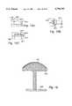
- FIG. 16is a cross-sectional view of an example of a dome-shaped palm button constructed in accordance with the present invention.
- FIG. 17is an electrical schematic of a touch circuit of the present invention implemented in a custom integrated circuit
- FIG. 18is an electrical schematic of an oscillator having a sleeper circuit for use in the capacitive responsive electronic switching circuits of the present invention.
- FIG. 19is a pictorial view of a device having two palm buttons and an indicator light operated in accordance with the present invention.
- FIGS. 20A-Care pictorial views of another embodiment of the device shown in FIG. 19.
- the touch circuit of present inventionoperates at a higher frequency than prior touch sensing circuits.
- a move to high frequency operation(>50 to 800 kHz) is not a benign choice relative to the lower frequency (60 to 1000 Hz) operation seen in existing art such as U.S. Pat. No. 4,758,735 and U.S. Pat. No. 5,087,825.
- Higher frequenciesrequire generally more costly, higher speed parts, and often results in the added cost of special design measures to minimize electronic emissions and the introduction of high frequency noise on power supply lines.
- the preference for using such higher frequenciesis based on a study performed to determine if high frequency operation would allow a touch of an operator and conduction via surface contamination films, such as moisture, providing a conductive path from a non-touched area to the touched area.
- the studyalso determined whether a high frequency touch circuit could operate over a sufficiently wide temperature range, an assortment of overlying dielectric layer thicknesses and materials, and in the presence of likely power supply fluctuations.
- the following calculations and measurementsare the results of this study.
- the resultssummarize the investigation conducted to reduce crosstalk due to condensation of water on the dielectric member (glass). By increasing the frequency of operation, the impedance of the body-glass combination is reduced as compared to the impedance of water between the touch pads.
- testing circuit 10includes an oscillator 20 coupled between ground plate and a 100 k ⁇ series resistor 22 and in parallel with a 10 M ⁇ resistor 24, a 20 pF capacitor 26, and contacts for connecting to a human body identified in the figure as an impedance load 15 having an impedance Z B representing the body's impedance.
- a human body's impedancemay be represented by the series combination of a 20-300 pF capacitor and a 1 k-2 k ⁇ resistor.
- testing circuit 30includes an oscillator 40 coupled in series with a 1 M ⁇ resistor 42 and contacts across which water is applied to define an impedance load 35 having an impedance Z w representing the impedance of water.
- a true RMS voltage meter 45is connected across the contacts of the impedance load 35.
- the capacitance of a piece of glass measuring 1/2" ⁇ 1/2" ⁇ 1/4"is approximately 2 pF.
- the equivalent circuit 50 of body touching the glass with the presence of wateris shown in FIG. 3.
- the equivalent circuit 50includes a polycarbon (PCB) plate 55 having at least two pads 57 and 59 formed thereon, a glass plate 60 adjacent to PCB plate 55, water 65 on glass plate 60 spanning at least two touch pad areas, and a body 70 in contact with the water 65 and glass plate 60 at one touch pad area.
- the impedance of glass plate 60is approximated by two 2 pF capacitors 62 and 64 connected to pads 57 and 59, respectively.
- the water 65is approximated by a 1 M ⁇ resistor 68 connected between capacitors 62 and 64.
- the bodyis represented by a 20-300 pF capacitor 72 coupled at one end to water resistor 68 and glass plate capacitor 62, and by a 1-2 k ⁇ resistor 74 coupled between the other end of capacitor 72 and ground.
- a human touch opposite pad 57will couple pad 57 to ground through the capacitance of glass 62 and the series contact with the human body impedance provided by the 20-300 pF capacitance and the 1 k-2 k ⁇ resistance of a typical human body. This will have the effect of pulling any voltage on the pad towards ground.
- Pad 59will be similarly effected, however it's coupling to ground will not only be through capacitance 64, and the series capacitance and resistance of the human body, but will also be through the ohmic resistance of water on the glass cover between the proximate location of pad 59 and the touched pad 57.
- the impedance of the path to ground for pads 57 and 59will be dominated by the glass and water impedances. If the impedance of the water path is significant compared to that of the glass, then the effect of a touch will be more significant at pad 57 than at pad 59.
- the impedance of the glassis preferably made as small as is practical compared to the impedance of the water. This allows discrimination between touched and adjacent pads. As the water impedance is primarily resistive and the glass impedance is primarily capacitive, the impedance of the glass will drop with frequency.
- FIG. 3Ashows the maximum and minimum glass impedance as a function of frequency.
- the maximum and minimum glass impedances shownwere computed as follows:
- the capacitive impedance of the glassis much greater than the nominal 1 M ⁇ of the water bridge between the pads.
- the glass impedancedrops to approximately 1 M ⁇ resulting in the impedance of the path to ground for pad 59 being twice that of the touched pad 57.
- a 100 kHz oscillator frequencywould allow a sufficiently low detection threshold to be set to differentiate between the signal changes induced at both pads by a human touch opposite a single pad.
- the impedance of the glassdrops to 200 k ⁇ or lower giving a ratio of a greater than 5 to 1 impedance difference between the paths to ground of the touched pad 57 and adjacent pads 59.
- the impedance ratiomay exceed 10 to 1, as illustrated in the calculation below. This allows the detection threshold for the touched pad to be set well below that of an adjacent pad resulting in a much lower incidence of inadvertent actuation of adjacent touch pads to that of the touched pad.
- the frequency of operationwould be kept at the 800 kHz of the preferred embodiment or even higher. However, as noted earlier, higher frequency operation forces the use of more expensive components and designs. For applications where thermal drift and electronic noise levels are low, operation at or near 100 kHz may be possible.
- the impedance of the glassbecomes much greater than that of likely water bridges between pads resulting in adjacent pads being effected as much by a touch as the touched pad itself.
- the preferred frequencyis at or above 100 kHz, and more preferably at or above 800 kHz, it is conceivable that frequencies as low as 50 kHz could be used provided the frequency creates a difference in the impedance paths of adjacent pads that is sufficient enough to accurately distinguish between an intended touch and the touch of an adjacent pad.
- Use of frequencies as low as 50 kHzmay also be possible depending upon the type of glass or covering or the thickness thereof used for the touch pad. However, in cases where there is little or no surface contamination, the frequency of operation can go well below 50 kHz.
- the frequency chosenwill be a tradeoff between the likelihood of surface contamination and the cost of going to higher frequencies to prevent cross talk due to such contamination.
- the following analysisillustrates one example of how a frequency may be calculated based on the typical parameters used to construct a touch switch and the typical impedance of a contaminant, such as rain water. In the analysis below a 10 to 1 ratio of water to glass impedance is sought.
- the impedance of body (Z B ) and glass (Z g ) combinationmust be much lower than impedance of water (Z W ). Since the impedance of glass is much higher than body impedance, Z g will be considered only. Therefore,
- the electronic switching circuitincludes a voltage regulator 100 including input lines 101 and 102 for receiving a 24 V AC line voltage and a line 103 for grounding the circuit.
- Voltage regulator 100converts the received AC voltage to a DC voltage and supplies a regulated 5 V DC power to an oscillator 200 via lines 104 and 105.
- Voltage regulatoralso supplies oscillator 200 with 26 V DC power via line 106.
- the details of voltage regulator 100are discussed below with reference to FIG. 5.
- oscillator 200Upon being powered by voltage regulator 100, oscillator 200 generates a square wave with a frequency of 50 kHz, and preferably greater than 800 kHz, and having an amplitude of 26 V peak.
- the square wave generated by oscillator 200is supplied via line 201 to a floating common generator 300, a touch pad shield plate 460, a touch circuit 400, and a microcontroller 500.
- Oscillator 200is described below with reference to FIG. 6.
- Floating common generator 300receives the 26 V peak square wave from oscillator 200 and outputs a regulated floating common that is 5 volts below the square wave output from oscillator 200 and has the same phase and frequency as the received square wave. This floating common output is supplied to touch circuit 400 and microcontroller 500 via line 301 such that the output square wave from oscillator 200 and floating common output from floating common generator 300 provide power to touch circuit 400 and microcontroller 500. Details of floating common generator 300 are discussed below with reference to FIG. 7.
- Touch circuit 400senses capacitance from a touch pad 450 via line 451 and outputs a signal to microcontroller 500 via line 401 upon detecting a capacitance to ground at touch pad 450 that exceeds a threshold value. The details of touch circuit 400 are described below with reference to FIG. 8.
- microcontroller 500Upon receiving an indication from touch circuit 400 that a sufficient capacitance to ground (typically at least 20 pF) is present at touch pad 450, microcontroller 500 outputs a signal to a load-controlling microcontroller 600 via line 501, which is preferably a two way optical coupling bus. Microcontroller 600 then responds in a predetermined manner to control a load 700. Having generally described the basic construction of the first embodiment, the preferred detailed construction of the depicted components will now be described with FIGS. 5-8. In cases where the number of lines to be switched is low, microcontroller 600 can be replaced by additional optical coupling lines.
- the number of lines to be switchedwill dictate whether it is more cost effective to multiplex over a two line optical bus such as line 501 and use a microcontroller to demultiplex, or to use a multiplicity of optical coupling lines. Other considerations such as reliability and power consumption may also affect this choice.
- the use of a single pair of optical coupling paths (line 501) and a microcontroller 600,is shown to emphasize the capability to switch a large number of lines.
- Voltage regulator 100preferably includes an AC/DC convertor 110 for generating 29 V to 36 V unregulated DC on line 119. This unregulated DC power is supplied to a 5 V DC regulator 120 and to a 26 V DC regulator 130.
- AC/DC convertor 110includes diodes 112, 114, 116, and 118, which rectify the supplied 24 V AC power provided on power lines 101 and 102.
- the anode of the first diode 112is coupled to power line 101 and to the cathode of the second diode 114.
- the cathode of the first diode 112is coupled to output line 119.
- the anode of the second diode 114is coupled to ground via line 103 and to the anode of the fourth diode 118.
- the anode of the third diode 116is coupled to the cathode of the fourth diode 118 and to power line 102.
- the cathode of the third diode 116is coupled to line 119 and to the cathode of the first diode 112.
- the anode of the fourth diode 118is coupled to ground via line 103.
- Diodes 112, 114, 116, and 118are preferably diodes having part no. 1N4002 available from LITEON.
- AC/DC convertor 110also preferably includes a capacitor 115 for filtering the rectified output of the diodes.
- Capacitor 115is preferably a 1000 ⁇ F capacitor coupled between output line 119 and ground via line 103.
- the 5 V regulator 120preferably includes a 500 ⁇ resistor 122 coupled between line 119 and 5 V output line 104, and a zener diode 124, a first capacitor 126, and second capacitor 128 all connected and parallel between output power lines 104 and 105.
- zener diode 124is a 5.1 V zener diode having part no. 1N4733A available from LITEON
- first capacitor 126has a capacitance of 10 ⁇ F
- second capacitor 128has a capacitance of 0.1 ⁇ F.
- the 26 V regulator 130preferably includes a transistor 134 having a collector connected to line 119 via a first resistor 132, a base connected to line 119 via a second resistor 136, and an emitter coupled to the regulated 26 V output power line 106.
- the 26 V regulator 130also preferably includes a capacitor 137 and zener diode 138 connected in parallel between the base of transistor 134 and ground line 103.
- first resistor 132is a 20 ⁇
- second resistor 136is a 1 k ⁇
- capacitor 137is a 0.1 ⁇ F capacitor
- zener diode 138is a 27 V, 0.5 W diode having part no.
- 1N5254Bavailable from LITEON. It will be apparent to those skilled in the art, that various components of voltage regulator 100 may be added or excluded depending upon the source of power available to power the oscillator 200. For example, if the available power is a 110 V AC 60 Hz commercial power line, a transformer may be added to convert the 110 V AC power to 24 V AC. Alternatively, if a DC battery is used, the AC/DC convertor among other components may be eliminated.
- Oscillator 200preferably includes a square wave generator 210, which is powered by 5 V regulator 120 via lines 104 and 105, for generating a 5 V peak square wave having the desired frequency, and a buffer circuit 230 powered by 26 V regulator 130 via line 106 for buffering the output of square wave generator 210 and boosting its peak from 5 V to 26 V while maintaining the preferred frequency.
- Square wave generator 210is preferably an astable multivibrator constructed with at least two serially connected invertor gates 212 and 214, and optionally, a third serially connected invertor gate 216.
- Invertor gates 212, 214 and 216are preferably provided in a single integrated circuit designated as part 74HC04 available from National Semiconductor.
- the output of the first invertor gate 212is coupled to it's input via resistors 218 and 222 and is coupled to the output of the second invertor gate 214 via a capacitor 224.
- the input of the second invertor gate 214is directly connected to the output of the first invertor gate 212 and the output of the second invertor gate 214 is directly connected to the input of the optional third invertor gate 216.
- resistor 218preferably has a 10.0 k ⁇ value
- resistor 222preferably has a 1.78 k ⁇ value
- capacitor 224is preferably a 220 pF capacitor.
- the 5 V peak square wave generated by square wave generator 210is supplied from either the output of invertor gate 214 or the output of optional invertor gate 216 to the base of a first transistor 238 via a first resistor 232 connected and parallel a capacitor 234.
- the base of first transistor 238is connected to the 26 V regulated DC power line 106 via a second resistor 236.
- the collector of first transistor 238is connected to 26 V power line 106 via a third resistor 240 and to the base of a second transistor 244.
- the emitter of first transistor 238is coupled to ground and to it's own collector and the base of second transistor 244 via a fourth resistor 242.
- the collector of the second transistor 244is connected directly to 26 V power line 106 and the emitter of second transistor 244 is connected to ground via a fifth resistor 246.
- Second transistor 244provides the 26 V peak square wave on output line 201, which is connected to it's emitter.
- the square wave signal applied to the base of transistor 238causes the collector of transistor 238 to swing between near to the DC supply 106 voltage and the collector-emitter saturation voltage.
- Capacitor 234is provided to improve the turning off of transistor 238.
- Transistor 244 along with resistors 242 and 246are used to buffer the square wave signal generated by transistor 238.
- the values of the resistors and capacitorare as follows: first resistor 232 is 5.1 k ⁇ , capacitor 234 is 0.0047 ⁇ F, second resistor 236 is 1 M ⁇ , third resistor 240 is 1.6 k ⁇ , fourth resistor 242 is 100 k ⁇ , and fifth resistor 246 is 4.7 k ⁇ .
- transistors 238 and 244are those identified as part no. ZTX600 available from ZETEX.
- the oscillator 200sources 80 mA to the floating common generator 300 such that together they supply a floating 5 V DC to power touch circuit(s) 400, microcontroller 500, and Schmitt triggered gates 420 (FIG. 8).
- oscillator 200may be varied from those disclosed above to provide for different oscillator output frequencies. As discussed above, however, oscillator 200 is preferably constructed so as to output a square wave having a frequency of 50 kHz or greater, and more preferably, of 800 kHz or greater. In some cases it may be necessary to use lower gain bandwidth product transistors or filtration to achieve a softer roll-off of the square edges to reduce high frequency noise emissions. When this is done the amplitude of the oscillator voltage can be increased to compensate.
- floating ground generator 300includes a zener diode 310 having a cathode connected to the oscillator output on line 201 and an anode connected to floating ground output line 301 and to ground via resistor 316 and diode 318.
- Floating ground generator 300also preferably includes a first capacitor 312 and a second capacitor 314 connected in parallel with zener diode 310.
- zener diode 310is a 5.1 V zener diode identified by part no.
- capacitor 312is a 47 ⁇ F tantalum capacitor
- capacitor 314is a 0.1 ⁇ F capacitor
- resistor 316is a 270 ⁇ resistor
- diode 318is a diode identified as part no. 1N914B available from LITEON.
- Touch circuit 400preferably includes a transistor 410 having a base connected to touch pad 450 via resistor 413 and line 451, an emitter coupled to oscillator output line 201, and a collector coupled to floating ground line 301 via a pulse stretcher circuit 417, which includes a resistor 416 and a capacitor 418 connected in parallel.
- a pulse stretcher circuit 417which includes a resistor 416 and a capacitor 418 connected in parallel.
- the physical length of the path between the touch pad 450 and the base of the transistor 410must be held to a minimum.
- RC filterscan be placed in line 401 between the output of the touch circuit 400 and the input of the microcontroller 500 to give additional EMI/RFI immunity. Additionally, the higher the frequency, the higher the gain bandwidth product that is required in transistor 410.
- the gain bandwidth productmust be sufficient to guarantee that the oscillator turns on during oscillator High pulses.
- a further trade-offis to use higher gain bandwidth product to allow lower oscillator voltages or higher oscillator voltages to all allow a lower gain bandwidth product transistor to be used.
- the combination of oscillator voltage, frequency and transistor gain bandwidth product that is usedwill necessarily vary with the cost, safety and reliability requirements of a given application. The present combination was chosen to keep the oscillator voltage down and allow operation at 800 kHz to minimize cross talk. At higher frequencies a higher gain bandwidth product transistor would be required in both the oscillator 200 and detection 400 circuits.
- Touch circuit 400also preferably includes resistor 412 and a diode 414 having an anode connected to the base of transistor 410 and to resistor 413, and a cathode connected to the emitter of transistor 410 and to a resistor 412 connected in parallel with diode 414 between the base and emitter of transistor 410.
- the pulse stretcher circuit 417is identified as such because the sensitivity of the touch circuit may be increased or decreased by varying the resistance of resistor 416.
- the base of transistor 410is connected via resistor 413 to line 451 connected to touch pad 450.
- touch circuit 400may include at least one Schmitt triggered gate 420 powered by the voltage difference existing between oscillator line 201 and 301, and having an input terminal coupled to the collector of transistor 410 and an output coupled to microcontroller 500 via output line 401.
- Schmitt triggered invertor gate 420is optionally provided to improve the rise time of the touch switch output and to buffer the output.
- transistor 410is part no. BC858CL available from Motorola
- resistor 412is a 12 M ⁇ resistor
- diode 414is part no. 1N914B available from Diodes, Inc.
- resistor 416is a 470 k ⁇ resistor
- capacitor 418is a 0.001 ⁇ F capacitor
- resistor 413is a 10 k ⁇ resistor.
- the operator's bodyincludes a capacitance to ground, which may range in a typical person from between 20 to 300 pF.
- the base terminal of transistor 410is coupled to it's emitter by resistor 412 such that unless capacitance is present by the user touching the touch pad 450, transistor 410 will not be forward biased and will not conduct.
- the output signal at the collector terminal of transistor 410 and across pulse stretcher circuit 417will be zero volts.
- a person touches the touch pad 450that person's body capacitance to ground couples the base of transistor 410 to ground 103 through resistor 413, thereby forward biasing transistor 410 into conduction.
- Diode 414is coupled across the base to emitter junction of transistor 410 to clamp the base emitter reverse bias voltage to -0.7 V and also reduce the forward recovery and turn-on time.
- Touch pad 450includes a substrate on which a plurality of electrically conductive plate members are mounted on one surface thereof.
- the substrateis an insulator and the plates are spaced apart in order to insulate the plates from one another and from ground.
- a guard bandpositioned on the substrate is a guard band, generally shown as 460.
- Guard band 460is a grid of conductor segments extending between adjacent pairs of plate members. All conductor segments are physically interconnected to define a plurality of spaces with one plate member positioned centrally within each space. Components of the touch circuit may be positioned on the side of substrate opposite plate members and guard band 460.
- a planar dielectric memberis spaced from the substrate facing plate members.
- the dielectric memberis made from a non-porous insulating material such as polycarbonate or glass.
- a plurality of electrically conductive spring contactsare sandwiched between the inner surface of the dielectric member and the substrate.
- An indicia layermay be adhered to the inner surface of the dielectric member to provide an indication of the function of each input portion.
- interface between the dielectric member and a conductive plateis a metallic spring contact that is attached to the back of the dielectric member.
- the spring contactsoffer advantages at high temperature extremes.
- conductive polymer foam pads cut to the size of the touch padsare preferably used to fill the gap between conductive pad and dielectric layer.
- the function of the spring contacts or conductive foam padsis to eliminate that capacitive contribution of the air filled gap between the conductive pads and the overlying dielectric layer.
- a problem with capacity responsive keyboardsis the tendency of switches that are closely positioned in a keyboard system to inadvertently become actuated even though the user is touching an adjacent switch. Furthermore, this problem is greatly aggravated by the presence of contamination on the outer surface of dielectric member. Contamination such as skin oil or moisture causes erratic keyboard operation and multiple switches will turn on even though one switch is touched.
- a high frequencysuch as 100 kHz or 800 kHz
- the impedance of the series combination of body and glass capacitanceare lowered as compared to the impedance of contamination present on the glass thereby reducing crosstalk.
- the touch circuitbecomes more sensitive to body capacitance.
- the oscillator circuitry shown in FIG. 6is very stable over the temperature range of -40° C. to 105° C.
- the output of the touch switch circuitrydrops at a rate of approximately 40 mV/°C. when temperature falls below 0° C.
- the following three methodsmay be used to increase the output of the switch: increase the oscillator's regulated supply voltage, increase the resistance of resistor 416, and use a higher gain transistor 410. All of these methods would increase sensitivity at high temperatures.
- Another way to correct this problemis to use a thermistor to vary the regulated supply voltage as a function of temperature.
- the circuit of FIG. 3was used to simulate glass, water resistance, and body capacitance. The following two conditions were simulated and tested:
- Table 4 belowshows the signal and noise voltages at the switch output for different values of body capacitance and contamination resistance.
- the circuitWith contamination resistance of 1 M ⁇ or more, the circuit is insensitive to body capacitance variations and has a minimum signal-to-noise ratio of -34 dB. With no contamination, signal-to-noise ratio is approximately -54 dB.
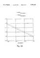
- the graph in FIG. 9shows the signal-to-noise ratio versus body capacitance, for different values of contamination resistance at 105° C. The minimum body capacitance to turn on a switch is 20 pF.
- the graph of FIG. 10shows the measured signal-to-noise ratio versus body capacitance, for different contamination resistance values at room temperature.
- the 20-300 pF of capacitance to ground offered by the human bodypresents a considerably lower impedance than the primarily resistive impedance of skin oil or water films that may appear on the dielectric layer overlying the conductive touch pads.
- Thisallows the peak voltage of a pad that is touched to come considerably closer to ground than adjacent pads which will have a voltage drop across any contaminating film layer that is providing a conductive path to the area that is touched.
- the enhanced sensitivity offered by the omission of any capacitor between the base and emitter of the detection transistor 410allows the threshold of detection to be set much closer to ground than would be the case otherwise.
- FIG. 11A multiple touch pad circuit constructed in accordance with the second embodiment is shown in FIG. 11.
- the multiple touch pad circuitis a variation of the first embodiment in that it includes an array of touch circuits designated as 900 1 through 900 nm , which, as shown, include both the touch circuit 400 shown in FIGS. 4 and 8 and the input touch terminal pad 451 (FIG. 4).
- Microcontroller 500selects each row of the touch circuits 900 1 to 900 nm by providing the signal from oscillator 200 to selected rows of touch circuits.
- microcontroller 500can sequentially activate the touch circuit rows and associate the received inputs from the columns of the array with the activated touch circuit(s).
- the detection circuits 900are physically located directly beneath the touch pads.
- a flexible circuit boardsuch as vended by Sheldahl, Inc. or Circuit Etching Technics, Inc. can be used for this purpose.
- the printed circuitwill be fixed directly against the surface (typically glass) bearing the conductive touch pads to eliminate air gaps and the need for conductive foam pads and spring contacts which were used to fill air gaps.
- the oscillator 200 of the first embodimentmay be slightly modified from that shown in FIG. 6 to include a transistor (not shown) coupled between the oscillator output and ground with it's base connected to microcontroller 600 such that microcontroller 600 may selectively disable the output of oscillator 200.
- the use of a high frequency in accordance with the present inventionprovides distinct advantages for circuits such as the multiple touch pad circuit of the present invention due to the manner in which crosstalk is substantially reduced without requiring any physical structure to isolate the touch terminals. Further, the reduction in crosstalk afforded by the present invention, allows the touch terminals in the array to be more closely spaced together.
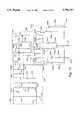
- the switching circuit according to the third embodimentincludes a voltage regulator 1100 for regulating power supplied by 24 V DC power lines 1101 and 1102 with ground connection 1103, for supplying the regulated power to an oscillator 1200 via lines 1104 and 1107.
- Oscillator 1200supplies a continuous and periodic signal to touch circuits 1400a and 1400b via line 1201.
- the frequency of the oscillator output signalis at least 100 kHz, and more preferably, at least 800 kHz.
- the two touch circuits 1400a and 1400bare identical in construction and both receive the output of touch terminal 1450 via line 1451.
- a detailed description of the preferred voltage regulator circuit 1100, oscillator 1200, and touch circuits 1400a and 1400bis provided below with reference to FIG. 13 following the description of the remaining portion of the third embodiment.
- the output of the first touch circuit 1400ais supplied to a first driver circuit 1500 via line 1401a while the output of the second touch circuit 1400b is supplied to a second driver circuit 1600 via line 1401b.
- the two driver circuits 1500 and 1600are provided to drive first and second serially connected switching transistors 1700 and 1710.
- the switching transistors 1700 and 1710must both be conducting to supply power to a relay switch 1800. Thus, if one of touch circuits 1400a and 1400b does not detect a touch of touch terminal 1450, one of switching transistors 1700 and 1710 will not conduct and power will not be supplied to relay switch 1800.
- the preferred construction of driver circuits 1500 and 1600 and relay switch 1800are described below with reference to FIG. 14.
- voltage regulator 1100may be constructed by providing a first capacitor 1110 and a varistor 1112 connected in parallel across input power terminals 1101 and 1102.
- return power terminal 1102is connected via line 1103 to ground.
- Varistor 1112is used to protect the circuit for over-voltage conditions.
- the voltage regulator 1100is reverse polarity protected by diode 1116 and current limited by resistor 1118.
- Capacitors 1120 and 1122provide filtering.
- Voltage regulator 1100further includes a zener diode 1128 having it's cathode connected to a node between resistor 1118 and capacitors 1120 and 1122 and to output power line 1104.
- the anode of zener diode 1128is coupled to output power common line 1107 and to ground line 1103 via two serially connected resistors 1124 and 1126.
- Zener diode 1128 and resistors 1124 and 1126generate regulated 15 V DC.
- Two capacitors 1130 and 1132are connected in parallel with zener diode 1128 between power lines 1104 and 1107. Capacitors 1130 and 1132 provide filtering and decoupling, respectively.
- capacitor 1110has a capacitance of 1000 pF, 1000V
- varistor 1112is part no. S14K25 available from Siemens
- fuse 1114is a 1/4A fuse
- diode 1116is part no. 1N4002 available from LITEON
- resistor 1118has a resistance of 10 ⁇ , 1/2W
- capacitor 1120has a capacitance of 22 ⁇ F, 35V
- capacitor 1122has a capacitance of 0.1 ⁇ F
- zener diode 1128is part no.
- resistor 1124has a resistance of 220 ⁇
- resistor 1126has a resistance of 220 ⁇
- capacitor 1130has a capacitance of 1 ⁇ F
- 25Vhas a capacitance of 0.1 ⁇ F.
- Oscillator 1200is preferably comprised of a first invertor gate 1210 having it's input coupled to it's output via resistors 1214 and 1216, and a second invertor gate 1212 having it's input coupled to the output of first invertor gate 1210 and it's output coupled to it's input via a capacitor 1218 and resistor 1216.
- the oscillating output of the second invertor gate 1212is buffered via transistor 1226, which has it's base connected to the output of second invertor gate 1212 via resistor 1220 and capacitor 1222, which are connected in parallel therebetween.
- the base of transistor 1226is also coupled to power line 1104 via a resistor 1224.
- the emitter of transistor 1226is connected to power line 1104 and the collector is connected to power line 1107 via a resistor 1230, to the anode of a diode 1228, and to the oscillator output line 1201.
- Diode 1228has it's cathode connected to power line 1104 and is used to protect transistor 1226.
- invertor gates 1210 and 1212are provided by part no. CD40106B available from Harris, resistor 1214 has a resistance of 10 k ⁇ , resistor 1216 has a resistance of 1.18 k ⁇ , 1%, capacitor 1218 has a capacitance of 220 pF, resistor 1220 has a resistance of 4.7 k ⁇ , capacitor 1222 has a capacitance of 220 pF, resistor 1224 has a resistance of 100 k ⁇ , transistor 1226 is part no. MMBTA70L available from Motorola, diode 1228 is part no. RLS4448 available from LITEON, and resistor 1230 has a resistance of 3.3 k ⁇ .
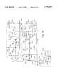
- Touch circuit 1400apreferably includes two resistors 1410a and 1412a coupled in series between touch terminal output line 1451 and the base of a bipolar PNP transistor 1420a.
- Transistor 1420ahas it's emitter connected to the oscillator output line 1201 and it's collector connected to power common line 1107 via a resistor 1422a.
- Touch circuit 1400afurther includes a diode 1414a, a capacitor 1416a, and a resistor 1418a all connected in parallel between the base of transistor 1420a and the emitter thereof, which is connected to oscillator output line 1201.
- Touch circuit 1400aalso includes a diode 1424a having it's anode connected to the collector of transistor 1420a and it's cathode connected to touch circuit output line 1401a via a resistor 1426a.
- resistor 1410ahas a resistance of 5.1 k ⁇
- resistor 1412ahas a resistance of 5.1 k ⁇
- diode 1414ais part no. RLS4448 available from LITEON
- capacitor 1416ahas a capacitance of 240 pF
- resistor 1418ahas a resistance of 12 M ⁇
- transistor 1420ais part no. BC857CL available from Motorola
- resistor 1422ahas a resistance of 100 k ⁇
- diode 1424ais part no. RLS4448 available from LITEON
- resistor 1426ahas a resistance of 100 k ⁇ .
- first driver circuit 1500the output line 1401a of first touch circuit 1400a is connected to power common line 1107 via a resistor 1510 and also via a capacitor 1512 connected in parallel therewith.
- the output line 1401ais also connected to the inverting input terminal of an operational amplifier 1514.
- the non-inverting input terminal of operational amplifier 1514is connected to line 1502, which runs between first and second driver circuits 1500 and 1600 and is connected to power line 1104 via a resistor 1626.
- the output of op amp 1514is connected to power line 1104 via a resistor 1518 and to the input of a Schmitt trigger invertor gate 1516.
- Schmitt trigger invertor gate 1516is connected to the input of a second Schmitt trigger invertor gate 1526 via a resistor 1520.
- a diode 1522is connected in parallel with resistor 1520 with it's cathode connected to the output of invertor gate 1516 and it's anode connected to the input of invertor gate 1526 and to power common line 1107 via capacitor 1524.
- the output of invertor gate 1526is connected to the base of bipolar PNP switching transistor 1700 via a resistor 1528.
- the base of transistor 1700is also connected to power common line 1107 via a capacitor 1532 and to power line 1104 and it's emitter via a resistor 1530.
- resistor 1510has a resistance of 10 M ⁇
- capacitor 1512has a capacitance of 0.01 ⁇ F
- op amp comparator 1514is part no. LM393 available from National Semiconductor
- invertor gate 1516is part no. CD40106B available from Harris
- resistor 1518has a resistance of 10 k ⁇
- resistor 1520has a resistance of 1 M ⁇
- diode 1522is part no.
- RLS4448available from LITEON
- capacitor 1524has a capacitance of 0.22 ⁇ F.
- invertor gate 1526is part no.
- resistor 1528has a resistance of 12 k ⁇
- resistor 1530has a resistance of 100 k ⁇
- capacitor 1532has a capacitance of 0.01 ⁇ F
- transistor 1700is part no. MMBTA56L available from Motorola.
- the output line 1401b of second touch circuit 1400bis connected to power common line 1107 via a resistor 1610 and also via a capacitor 1612 connected in parallel therewith.
- the output line 1401bis also connected to the inverting input terminal of an operational amplifier 1614.
- the non-inverting input terminal of operational amplifier 1614is connected to line 1502, which is connected to power line 1104 via resistor 1626.
- the non-inverting input terminal of op amp 1614is also connected to power common line 1107 via a capacitor 1616 and a resistor 1618, which are connected in parallel.
- the output of op amp 1614is connected to power line 1104 via a resistor 1630 and to the coupled inputs of a Schmitt trigger invertor gate 1628.
- the output of op amp 1614is also connected to it's non-inverting input terminal via a resistor 1624.
- the output of Schmitt trigger invertor NAND gate 1628is connected to the input of a second Schmitt trigger invertor gate 1638 via a resistor 1632.
- a diode 1634is connected in parallel with resistor 1632 with it's cathode connected to the output of invertor NAND gate 1628 and it's anode connected to the input of invertor NAND gate 1638 and to power common line 1107 via a capacitor 1636.
- the output of invertor gate 1638is connected to the base of switching bipolar PNP transistor 1710 via a resistor 1640.
- Second driver circuit 1600also preferably includes capacitors 1620 and 1622 connected in parallel between it's connections to power lines 1104 and 1107.
- resistor 1610has a resistance of 10 M ⁇
- capacitor 1612has a capacitance of 0.01 ⁇ F
- op amp comparator 1614is part no. LM393 available from National Semiconductor
- capacitor 1616has a capacitance of 0.01 ⁇ F
- resistor 1618has a resistance of 20 k ⁇
- capacitor 1620has a capacitance of 0.1 ⁇ F
- capacitor 1622has a capacitance of 0.1 ⁇ F
- resistor 1624has a resistance of 100 k ⁇
- resistor 1626has a resistance of 10 k ⁇
- invertor NAND gate 1628is part no.
- CD4093Bavailable from Harris
- resistor 1630has a resistance of 10 k ⁇
- resistor 1632has a resistance of 1 M ⁇
- diode 1634is part no.
- RLS4448available from LITEON
- capacitor 1636has a capacitance of 0.22 ⁇ F
- invertor NAND gate 1638is part no.
- CD4093Bavailable from Harris
- resistor 1640has a resistance of 12 k ⁇
- capacitor 1642has a capacitance of 0.01 ⁇ F
- resistor 1644has a resistance of 100 k ⁇
- transistor 1710is part no.
- MMBTA56Lavailable from Motorola.
- the output of transistor 1420a(FIG. 13) taken at it's collector is rectified by diode 1424a and a DC level is generated by resistors 1426a and 1510 and capacitor 1512 (a DC level of the output of transistor 1420b is generated by resistors 1426b and 1610 and capacitor 1612).
- a DC level of the output of transistor 1420bis generated by resistors 1426b and 1610 and capacitor 1612.
- the output of schmitt triggered invertor gate 1516 inverter NAND gate 1628 (1628)goes high which charges capacitor 1524 (1636) through resistor 1520 (1632).
- Gates 1516 and 1526 (1628 and 1638), resistor 1520 (1632), and capacitor 1524 (1636)provide debounce in a conventional manner.
- Diode 1522 (1634)is used to provide fast release when the palm of the hand is removed from the touch terminal 1450.
- the output of the debounce circuitrydrives transistor 1700 (1710).
- Resistor 1528 (1640) and capacitor 1532 (1642)are used to filter noise. Both touch circuits must be functional in order to drive the relay switch 1800. Also, if one of the transistors 1700 or 1710 fails, the relay will not be activated.
- Relay switch 1800may be any conventional relay. An example of such a relay is shown in FIG. 14.
- Relay switch 1800may include a relay coil 1810 coupled between the selective power supply 1711 of transistors 1700 and 1710 and ground, and a pair of magnetically responsive switches that switch from normally closed terminals 1805 and 1807 to normally open terminals 1801 and 1803 when the relay coil is energized.
- a zener diode 1815may be placed in series with a diode 1820 to reduce stress on the relay coil 1810 and to protect transistor 1710 when transistors 1700 and 1710 switch off.
- touch circuits of the third embodimentare disclosed as operating a relay switch via driver circuits, it will be appreciated by those skilled in the art that the outputs of touch circuits 1400a and 1400b could be supplied to a microcontroller in the manner discussed above with respect to the first embodiment.
- the palm button switch of the present inventionuses two redundant touch switch circuits, such as shown in FIG. 12, to disable relay drivers if one of the touch switch circuits fails and redundant relay driver circuitry to turn off a relay switch if one of the driver circuits fails.
- a method to prevent inadvertent actuationsis to require a multi-step process.
- a deviceis shown having a first palm button 2201, a second palm button 2202, and an indicator light 2205. Palm button 2201 has to be activated first and then button 2202 has to be activated within a 2 second time window before a desired actuation can occur.
- the 90 degree orientation of the two buttonsmakes it extremely difficult to accidently touch both with an arm and an elbow or other such physical combination.
- buttons 2201 to button 2202can provide some relief from fatigue in the forearm by the resulting muscle flexure that would otherwise not occur if the hand had to be kept near a single button for extended periods of time.
- a further redundancycan be achieved by requiring simultaneous operation of two such devices, one for each hand. This provides further safeguards against inadvertent actuations and forces the operator to have both hands in a desired safe location once a desired actuation occurs.
- a further optionis to provide one or more LEDs 2205 or audible annunciators for visual or audible feedback to the operator. Specifically, in FIG.
- the LED 2205will come on when button 2201 has been successfully activated to cue the operator that it is time to move to button 2202.
- a second LED with a different color than the firstcan be provided to provide visual confirmation that the second button 2202 has been activated or that the required combination of the two buttons has been activated.
- Two different audible tone or sound generatorscould also be used in lieu of the LEDs to provide feedback to the operator.
- the housingis made of high strength polycarbonate (or other high strength non-metallic material) to meet high impact and vibration requirements, preferably NEMA 4.
- a further optionis to provide lighting for the switches to allow operation in the dark.
- two touch plates within a housingare used to provide a two-step turn-on.
- the first step to actuate the output relay 2310is initiated when the operator inserts his hands and touches the vertical touch sensor 2301 with the dorsal side of the hands.
- a yellow LED 2304 on top of the deviceshow the successful completion of the first step.
- the second stepis to flip the hand over and touch the horizontal touch sensor 2302 with the palmar side of the hand.
- a red LED 2305 on top of the deviceshows the completion of the two step turn-on and activation of output relay 2310.
- the flipping action of the hand in the second stepcauses the forearm muscles to flex, thereby reducing stiffness and fatigue. Also, the hands, and arms can rest on the run bar until the machine cycle is complete.
- the second step of the two-step turn-onmust occur within some predetermined time (for example 2 seconds) after the release of vertical touch sensor or the first step must be repeated. In this proposed embodiment, the second step provides an added stimulus and reduces operator errors due to mental and physical fatigue.
- the top coverprevents actuation of two devices by the use of one hand and elbow of the same arm, as required by ANSI Standard B11.19-1990.
- the enclosuremust be a high strength polycarbonate module to meet the high impact and vibration requirements of the industry, preferably NEMA 4.
- the palm buttonmay be formed as the flat palm button shown in FIGS. 15A-C or as a dome-shaped palm button shown in FIG. 16.
- the buttonis made of a brass plate 1910 (1930) and can be covered with a plastic or glass 1925 (1933) cover or membrane to desensitize the unit even more against contaminants and other inadvertent actuation.
- the plastic cover 1925 (1933)acts as a dielectric and capacitance is varied as a function of the area of the plastic being touched. Therefore, if button is touched by finger, a much smaller series capacitance is generated as opposed to button being touched by the palm of a hand.
- This capacitanceis placed in series with the capacitance of the body to ground when the button is touched. Since the capacitance of the body to ground is much larger than the capacitance generated by the button, the functionality of the unit is independent of the variations in body capacitance to ground from person to person. The other factor that needs to be considered here is body resistance. If the button is not covered with an insulator such as plastic, the unit would become sensitive to body resistance. Body resistance to ground, changes as a function of moisture in the work area, skin dryness, floor structure, and shoes. By using a plastic cover, the unit is made insensitive to variations of body resistance and capacitance. The shape of the button is also a factor in sensitivity.
- the buttonis flat, less of the button area would be covered by the palm of the hand as opposed to a dome shape button that matches the contour of the palm. Therefore, if the button is dome-shaped, the unit can be even more desensitized against inadvertent operation.
- the palm button of the present inventioncan be activated with or without gloves.
- the zero force palm button of the present inventionmay be used to activate electric, pneumatic, air clutch, and hydraulic equipment such as punch presses, molding machines, etc.
- the flat palm buttonmay include a plastic housing 1917 having an optional metallic enclosure 1922 for surface mounting.
- the buttonalso may include a flush mount surface 1915 and optional guarding 1920.
- the circuit board 1935 used with the palm button of the present inventionmay be packaged on two printed circuit boards. One board for power and relay and the other for touch switches and relay drivers.
- the touch circuit on the touch switch boardis interfaced to the button through a screw that also holds the button in place.
- the power/relay boardis interfaced to the touch switch board through a three pin right angle connector. Wiring to the unit is done through a seven position terminal block on the power/relay board.
- the power/relay boardis designed for 24 V DC input power and provides two double-throw relay contacts. However, it can be modified to accommodate different power inputs and switch outputs. For example, a transformer may be added to the power board so that the unit is powered 110VAC/220VAC instead of 24 V DC. Also, the relays may be replaced with other outputs such as digital or 4-20 mA outputs.
- the touch circuit componentscan be integrated in a custom IC 2000, as shown in FIG. 17, to facilitate manufacturing and to reduce cost.
- Components 413, 412, 414, 410, 418, and 420are similar to those of circuit 400 shown in FIG. 8.
- resistor 2004has a resistance of 470 k ⁇ and diode 2002 has characteristics similar to part no. 1N4148 available from LITEON.
- Resistors 2008 and 2006are used to adjust the sensitivity.
- Diode 2002 at the output of 420allows the IC to be used in applications where several touch circuit IC's are multiplexed.
- a sleep circuit 2100may be added to the oscillator circuit 200 (FIG. 6) to allow microcontroller 600 to turn off the oscillator circuit 200.
- the disabling of oscillator circuit 200is done to reduce drainage of capacitor 126 in the regulator circuit 120 during brown outs.
- the circuit diagram shown in FIG. 18is a modified version of circuit 200 in FIG. 6.
- microcontroller 600pulls the input of gate 2116 to ground and causes the output of gate 2116 to go high (power line 104). Therefore, transistor 2110 is biased on and oscillator 200 is functional.
- microcontroller 600sources the input to gate 2116 high and causes the output of gate 2116 to go low which turns off transistor 2110 and pulls the input of gate 212 low. Therefore, the oscillator will stop oscillating and drainage on capacitor 126 decreases considerably.
Landscapes
- Electronic Switches (AREA)
Abstract
Description
TABLE 1 ______________________________________ CONCRETE SLAB CONCRETE SLAB SUBFLOOR SUBFLOOR ______________________________________ 1.4 kΩ 100 pF 1.7 kΩ 73 pF 1.4 kΩ 217 pF 1.9 kΩ 78 pF 1.3 kΩ 174 pF 1.9 kΩ 93 pF 1.2 kΩ 160 pF 1.6 kΩ 85 pF 1.0 kΩ 107 pF 1.4 kΩ 75 pF ______________________________________
K.sub.a =0.08842×10.sup.-6 for vacuum
6.0<K.sub.glass <10
A=0.25 in.sup.2
L=0.25 in
C.sub.max =10×0.08842×10.sup.-6 ×2.54×10.sup.-6 =2.25 pF
C.sub.min =6×0.08842×10.sup.-6 ×2.54×10.sup.-6 =1.35 pF
TABLE 2 ______________________________________ Dielectric Constant TYPE OF GLASS (K) ______________________________________ Corning 0010 6.32 Corning 0080 6.75 Corning 0120 6.65 Corning 8870 9.5 ______________________________________
e.sub.o =8.854×10.sup.-12 C.sup.2 /(nm.sup.2)
K.sub.gmin =6
K.sub.gmax =10
A=0.25 in.sup.2
L=0.25 in
C.sub.max =K.sub.gmax e.sub.0 A/L C.sub.max =2.249 pF
C.sub.min =K.sub.gmin e.sub.0 A/L C.sub.min =1.349 pF
Zgmin.sub.frequency =1/(2 πC.sub.max frequency)
Zgmax.sub.frequency =1/(2 πC.sub.min frequency)
10|Z.sub.g |<|Z.sub.W |Eq. 3
C.sub.glass =2 pF Z.sub.W =1 MΩ ##EQU4## Therefore,
ƒ>796 kHz
TABLE 3 ______________________________________ SUPPLY VOLTAGE SWITCH OUTPUT ______________________________________ 36 VDC 4.96V 35 VDC 4.96 V 34 VDC 4.95 V 33 VDC 4.95 V 32 VDC 4.94 V 31 VDC 4.93V 30 VDC 4.93 V 29 VDC 4.92 V ______________________________________
PSRR=6 mV/V=-45 dB
TABLE 4 ______________________________________ CONTAM- INATION RE- BODY CAPACITANCE SISTANCE 20pF 220pF 330pF 550pF 1230 pF ______________________________________ 330 kΩ S: 5.1 V S: 5.1 V S: 5.1 V S: 5.1 V S: 5.1 V N: 2.0 V N: 4.0 V N: 4.5 V N: 4.9 V N: 5.0V 500 kΩ S: 5.1 V S: 5.1 V S: 5.1 V S: 5.1 V S: 5.1 V N: 0.2 V N: 0.6 V N: 0.7 V N: 0.8 V N: 0.8V 1 MΩ S: 5.1 V S: 5.1 V S: 5.1 V S: 5.1 V S: 5.1 V (Condensed N: 0.1 V N: 0.1 V N: 0.1 V N: 0.1 V N: 0.1 V Water) NONE S: 5.1 V S: 5.1 V S: 5.1 V S: 5.1 V S: 5.1 V N: 10 mV N: 10 mV N: 10 mV N: 10 mV N: 10 mV ______________________________________ S = Signal (TOUCH) N = Noise (NO TOUCH) supply voltage = 36 VDC temperature = 105° C.
TABLE 5 ______________________________________ CONTAM- INATION RE- BODY CAPACITANCE SISTANCE 20pF 220pF 330pF 550pF 1230 pF ______________________________________ 200 kΩ S: 5.1 V S: 5.1 V S: 5.1 V S: 5.1 V S: 5.1 V N: 0.2 V N: 1.0 V N: 1.2 V N: 1.8 V N: 2.2 V 250 kΩ S: 5.1 V S: 5.1 V S: 5.1 V S: 5.1 V S: 5.1 V N: 0.1 V N: 0.1 V N: 0.5 V N: 0.5 V N: 0.5V 330 kΩ S: 5.1 V S: 5.1 V S: 5.1 V S: 5.1 V S: 5.1 V N: 0.1 V N: 0.1 V N: 0.1 V N: 0.1 V N: 0.1V 1 MΩ S: 5.1 V S: 5.1 V S: 5.1 V S: 5.1 V S: 5.1 V (Condensed N: 0.1 V N: 0.1 V N: 0.1 V N: 0.1 V N: 0.1 V Water) ______________________________________ S = Signal (TOUCH) N = Noise (NO TOUCH) supply voltage = 36 VDC temperature = 25° C.
Claims (32)
Priority Applications (2)
| Application Number | Priority Date | Filing Date | Title |
|---|---|---|---|
| US08/601,268US5796183A (en) | 1996-01-31 | 1996-01-31 | Capacitive responsive electronic switching circuit |
| DE19703404ADE19703404B4 (en) | 1996-01-31 | 1997-01-30 | Capacitive reaction electronic circuit |
Applications Claiming Priority (1)
| Application Number | Priority Date | Filing Date | Title |
|---|---|---|---|
| US08/601,268US5796183A (en) | 1996-01-31 | 1996-01-31 | Capacitive responsive electronic switching circuit |
Publications (1)
| Publication Number | Publication Date |
|---|---|
| US5796183Atrue US5796183A (en) | 1998-08-18 |
Family
ID=24406854
Family Applications (1)
| Application Number | Title | Priority Date | Filing Date |
|---|---|---|---|
| US08/601,268Expired - LifetimeUS5796183A (en) | 1996-01-31 | 1996-01-31 | Capacitive responsive electronic switching circuit |
Country Status (2)
| Country | Link |
|---|---|
| US (1) | US5796183A (en) |
| DE (1) | DE19703404B4 (en) |
Cited By (162)
| Publication number | Priority date | Publication date | Assignee | Title |
|---|---|---|---|---|
| US5973417A (en)* | 1997-02-17 | 1999-10-26 | E.G.O. Elektro-Geraetebau Gmbh | Circuit arrangement for a sensor element |
| US6282909B1 (en) | 1995-09-01 | 2001-09-04 | Nartron Corporation | Ice making system, method, and component apparatus |
| EP1164697A1 (en)* | 2000-06-13 | 2001-12-19 | Lg Electronics Inc. | Glass touch sensing circuit |
| US6452494B1 (en)* | 1999-09-27 | 2002-09-17 | Intel Corporation | Activating devices |
| US6499359B1 (en) | 2001-07-09 | 2002-12-31 | Nartron Corporation | Compressible capacitance sensor for determining the presence of an object |
| US20030019886A1 (en)* | 2001-01-19 | 2003-01-30 | Lancer Partnership. Ltd | Customer interface for a beverage dispenser |
| US20030056600A1 (en)* | 2001-07-09 | 2003-03-27 | Nartron Corporation | Anti-entrapment system |
| US6608617B2 (en) | 2000-05-09 | 2003-08-19 | Marc O. Hoffknecht | Lighting control interface |
| WO2004001560A1 (en)* | 2002-06-19 | 2003-12-31 | Nokia Corporation | Method of deactivating lock, and portable electronic device |
| US20040056845A1 (en)* | 2002-07-19 | 2004-03-25 | Alton Harkcom | Touch and proximity sensor control systems and methods with improved signal and noise differentiation |
| US6713897B2 (en)* | 1999-01-19 | 2004-03-30 | Touchsensor Technologies, Llc | Touch switch with integral control circuit |
| US20040189100A1 (en)* | 2003-03-25 | 2004-09-30 | Gasperi Michael Lee | Method and apparatus for providing a switching signal in the presence of noise |
| US20040195919A1 (en)* | 2003-04-02 | 2004-10-07 | Gasperi Michael Lee | Method and apparatus for providing a switching signal in the presence of noise |
| US20050062732A1 (en)* | 2001-03-30 | 2005-03-24 | Microsoft Corporation | Capacitance touch slider |
| US20050068646A1 (en)* | 2003-09-25 | 2005-03-31 | Homedics, Inc. | Mirror with adjustable magnification and with a plurality of displays and devices |
| US20050068078A1 (en)* | 2003-04-22 | 2005-03-31 | Steenwyk Timothy Edward | Electronic door latch system with water rejection filtering |
| US20050092097A1 (en)* | 2001-07-09 | 2005-05-05 | Nartron Corporation | Anti-entrapment system |
| US20050184749A1 (en)* | 2004-02-24 | 2005-08-25 | Hitachi High-Technologies Corporation | Control system and method of semiconductor inspection system |
| US20060087314A1 (en)* | 2004-10-26 | 2006-04-27 | Georgia Tech Research Corporation | Displacement sensor |
| US20060117862A1 (en)* | 2004-12-06 | 2006-06-08 | Shank David W | Anti-entrapment system |
| US20060117661A1 (en)* | 2002-09-12 | 2006-06-08 | Goran Hansson | Capacitive squeeze protecting device |
| US20060158041A1 (en)* | 1999-01-19 | 2006-07-20 | Caldwell David W | Touch switches and practical applications therefor |
| US20060174858A1 (en)* | 2005-02-04 | 2006-08-10 | Denso Corporation | Ignition apparatus for internal combustion engine |
| US20060202651A1 (en)* | 2005-03-11 | 2006-09-14 | Washeleski John M | Powered panel moving system |
| US20060273806A1 (en)* | 2004-02-17 | 2006-12-07 | Gustav Magenwirth Gmbh & Co. Kg | Operator sensing circuit for disabling motor of power equipment |
| US20070018509A1 (en)* | 2005-07-20 | 2007-01-25 | Ewig Industries Macao Commercial Offshore Limited | Device having multiple conductive contact switches |
| US20070070524A1 (en)* | 2005-09-28 | 2007-03-29 | Nikon Corporation | High zoom ratio zoom lens system |
| US20070089527A1 (en)* | 2001-07-09 | 2007-04-26 | Nartron Corporation | Anti-entrapment system |
| US20070152615A1 (en)* | 2006-01-04 | 2007-07-05 | Nartron Corporation | Vehicle panel control system |
| US20070176903A1 (en)* | 2006-01-31 | 2007-08-02 | Dahlin Jeffrey J | Capacitive touch sensor button activation |
| US7253643B1 (en) | 2006-07-19 | 2007-08-07 | Cypress Semiconductor Corporation | Uninterrupted radial capacitive sense interface |
| US20070186663A1 (en)* | 2006-02-13 | 2007-08-16 | Samsung Electronics Co., Ltd. | Apparatus, method, and medium for adaptively setting reference sensing boundary of touch sensor |
| US7307485B1 (en) | 2005-11-14 | 2007-12-11 | Cypress Semiconductor Corporation | Capacitance sensor using relaxation oscillators |
| US7312616B2 (en) | 2006-01-20 | 2007-12-25 | Cypress Semiconductor Corporation | Successive approximate capacitance measurement circuit |
| US20080194909A1 (en)* | 2007-02-13 | 2008-08-14 | Brown Stuart I | Holding device for medical purposes |
| US20090021267A1 (en)* | 2006-07-17 | 2009-01-22 | Mykola Golovchenko | Variably dimensioned capacitance sensor elements |
| US7483252B2 (en) | 2006-12-05 | 2009-01-27 | Ferraz Shawmut S.A. | Circuit protection device |
| US20090058430A1 (en)* | 2007-09-05 | 2009-03-05 | Sentrinsic | Systems and Methods for Sensing Positions of Components |
| US20090107493A1 (en)* | 2007-10-29 | 2009-04-30 | Smiths Medical Asd, Inc. | Redundant power control for respiratory system heaters |
| US20090165690A1 (en)* | 2008-01-02 | 2009-07-02 | Walworth Christopher J | Sports board |
| US7593000B1 (en) | 2008-05-17 | 2009-09-22 | David H. Chin | Touch-based authentication of a mobile device through user generated pattern creation |
| US20090266605A1 (en)* | 2006-06-20 | 2009-10-29 | Abb Research Ltd. | High voltage valve group with increased breakdown strength |
| US20100044604A1 (en)* | 2007-03-28 | 2010-02-25 | Masco Corporation Of Indiana | Capacitive touch sensor |
| US20100053093A1 (en)* | 2008-08-27 | 2010-03-04 | Jing Kong | Multi-point touch-sensitive system |
| US7721609B2 (en) | 2006-03-31 | 2010-05-25 | Cypress Semiconductor Corporation | Method and apparatus for sensing the force with which a button is pressed |
| US7737724B2 (en) | 2007-04-17 | 2010-06-15 | Cypress Semiconductor Corporation | Universal digital block interconnection and channel routing |
| US7761845B1 (en) | 2002-09-09 | 2010-07-20 | Cypress Semiconductor Corporation | Method for parameterizing a user module |
| US7765095B1 (en) | 2000-10-26 | 2010-07-27 | Cypress Semiconductor Corporation | Conditional branching in an in-circuit emulation system |
| US7770113B1 (en) | 2001-11-19 | 2010-08-03 | Cypress Semiconductor Corporation | System and method for dynamically generating a configuration datasheet |
| US7774190B1 (en) | 2001-11-19 | 2010-08-10 | Cypress Semiconductor Corporation | Sleep and stall in an in-circuit emulation system |
| US7825688B1 (en) | 2000-10-26 | 2010-11-02 | Cypress Semiconductor Corporation | Programmable microcontroller architecture(mixed analog/digital) |
| US20100297930A1 (en)* | 2009-05-20 | 2010-11-25 | Harris Technology, Llc | Portable Device with a Vehicle driver Detection |
| US7844437B1 (en) | 2001-11-19 | 2010-11-30 | Cypress Semiconductor Corporation | System and method for performing next placements and pruning of disallowed placements for programming an integrated circuit |
| US7893724B2 (en) | 2004-03-25 | 2011-02-22 | Cypress Semiconductor Corporation | Method and circuit for rapid alignment of signals |
| USRE42319E1 (en) | 1998-06-08 | 2011-05-03 | Mersen France Sb Sas | Circuit protection device |
| US20110227837A1 (en)* | 2010-03-16 | 2011-09-22 | E Ink Holdings Inc. | Electromagnetic touch displayer |
| US8026739B2 (en) | 2007-04-17 | 2011-09-27 | Cypress Semiconductor Corporation | System level interconnect with programmable switching |
| US8040142B1 (en) | 2006-03-31 | 2011-10-18 | Cypress Semiconductor Corporation | Touch detection techniques for capacitive touch sense systems |
| US8040321B2 (en) | 2006-07-10 | 2011-10-18 | Cypress Semiconductor Corporation | Touch-sensor with shared capacitive sensors |
| US8040266B2 (en) | 2007-04-17 | 2011-10-18 | Cypress Semiconductor Corporation | Programmable sigma-delta analog-to-digital converter |
| US8049569B1 (en) | 2007-09-05 | 2011-11-01 | Cypress Semiconductor Corporation | Circuit and method for improving the accuracy of a crystal-less oscillator having dual-frequency modes |
| US8058937B2 (en) | 2007-01-30 | 2011-11-15 | Cypress Semiconductor Corporation | Setting a discharge rate and a charge rate of a relaxation oscillator circuit |
| US8067948B2 (en) | 2006-03-27 | 2011-11-29 | Cypress Semiconductor Corporation | Input/output multiplexer bus |
| US8069436B2 (en) | 2004-08-13 | 2011-11-29 | Cypress Semiconductor Corporation | Providing hardware independence to automate code generation of processing device firmware |
| US8069405B1 (en) | 2001-11-19 | 2011-11-29 | Cypress Semiconductor Corporation | User interface for efficiently browsing an electronic document using data-driven tabs |
| US8069428B1 (en) | 2001-10-24 | 2011-11-29 | Cypress Semiconductor Corporation | Techniques for generating microcontroller configuration information |
| US8078894B1 (en) | 2007-04-25 | 2011-12-13 | Cypress Semiconductor Corporation | Power management architecture, method and configuration system |
| US8078970B1 (en) | 2001-11-09 | 2011-12-13 | Cypress Semiconductor Corporation | Graphical user interface with user-selectable list-box |
| US8085100B2 (en) | 2005-02-04 | 2011-12-27 | Cypress Semiconductor Corporation | Poly-phase frequency synthesis oscillator |
| US8085067B1 (en) | 2005-12-21 | 2011-12-27 | Cypress Semiconductor Corporation | Differential-to-single ended signal converter circuit and method |
| US8086417B2 (en) | 2007-07-03 | 2011-12-27 | Cypress Semiconductor Corporation | Normalizing capacitive sensor array signals |
| US8089472B2 (en) | 2006-05-26 | 2012-01-03 | Cypress Semiconductor Corporation | Bidirectional slider with delete function |
| US8089289B1 (en) | 2007-07-03 | 2012-01-03 | Cypress Semiconductor Corporation | Capacitive field sensor with sigma-delta modulator |
| US8089461B2 (en) | 2005-06-23 | 2012-01-03 | Cypress Semiconductor Corporation | Touch wake for electronic devices |
| US8089288B1 (en) | 2006-11-16 | 2012-01-03 | Cypress Semiconductor Corporation | Charge accumulation capacitance sensor with linear transfer characteristic |
| US8092083B2 (en) | 2007-04-17 | 2012-01-10 | Cypress Semiconductor Corporation | Temperature sensor with digital bandgap |
| US8103496B1 (en) | 2000-10-26 | 2012-01-24 | Cypress Semicondutor Corporation | Breakpoint control in an in-circuit emulation system |
| US8103497B1 (en) | 2002-03-28 | 2012-01-24 | Cypress Semiconductor Corporation | External interface for event architecture |
| US8120408B1 (en) | 2005-05-05 | 2012-02-21 | Cypress Semiconductor Corporation | Voltage controlled oscillator delay cell and method |
| US20120050214A1 (en)* | 2010-08-24 | 2012-03-01 | Viktor Kremin | Reducing water influence on a touch-sensing device |
| US8130025B2 (en) | 2007-04-17 | 2012-03-06 | Cypress Semiconductor Corporation | Numerical band gap |
| US8144126B2 (en) | 2007-05-07 | 2012-03-27 | Cypress Semiconductor Corporation | Reducing sleep current in a capacitance sensing system |
| US8149048B1 (en) | 2000-10-26 | 2012-04-03 | Cypress Semiconductor Corporation | Apparatus and method for programmable power management in a programmable analog circuit block |
| US8160864B1 (en) | 2000-10-26 | 2012-04-17 | Cypress Semiconductor Corporation | In-circuit emulator and pod synchronized boot |
| US8169238B1 (en) | 2007-07-03 | 2012-05-01 | Cypress Semiconductor Corporation | Capacitance to frequency converter |
| US8176296B2 (en) | 2000-10-26 | 2012-05-08 | Cypress Semiconductor Corporation | Programmable microcontroller architecture |
| US8286125B2 (en) | 2004-08-13 | 2012-10-09 | Cypress Semiconductor Corporation | Model for a hardware device-independent method of defining embedded firmware for programmable systems |
| US20120281443A1 (en)* | 2009-09-11 | 2012-11-08 | Sma Solar Technology Ag | Inverter device comprising a topology surveying a series of capacitors |
| US8321174B1 (en) | 2008-09-26 | 2012-11-27 | Cypress Semiconductor Corporation | System and method to measure capacitance of capacitive sensor array |
| US8358142B2 (en) | 2008-02-27 | 2013-01-22 | Cypress Semiconductor Corporation | Methods and circuits for measuring mutual and self capacitance |
| US8402313B1 (en) | 2002-05-01 | 2013-03-19 | Cypress Semiconductor Corporation | Reconfigurable testing system and method |
| US20130123763A1 (en)* | 2006-03-27 | 2013-05-16 | Lutronic Corporation | Control method and structure of laser beam irradiation by using a contact sensor |
| US8454181B2 (en) | 2010-08-25 | 2013-06-04 | Ford Global Technologies, Llc | Light bar proximity switch |
| US8477468B2 (en) | 2011-11-04 | 2013-07-02 | Mersen Usa Newburyport-Ma, Llc | Circuit protection device |
| US8487639B1 (en) | 2008-11-21 | 2013-07-16 | Cypress Semiconductor Corporation | Receive demodulator for capacitive sensing |
| US8487912B1 (en) | 2008-02-01 | 2013-07-16 | Cypress Semiconductor Corporation | Capacitive sense touch device with hysteresis threshold |
| US8493351B2 (en) | 2006-03-30 | 2013-07-23 | Cypress Semiconductor Corporation | Apparatus and method for reducing average scan rate to detect a conductive object on a sensing device |
| US8499270B1 (en) | 2007-04-25 | 2013-07-30 | Cypress Semiconductor Corporation | Configuration of programmable IC design elements |
| US8516025B2 (en) | 2007-04-17 | 2013-08-20 | Cypress Semiconductor Corporation | Clock driven dynamic datapath chaining |
| US8525798B2 (en) | 2008-01-28 | 2013-09-03 | Cypress Semiconductor Corporation | Touch sensing |
| US8527949B1 (en) | 2001-11-19 | 2013-09-03 | Cypress Semiconductor Corporation | Graphical user interface for dynamically reconfiguring a programmable device |
| US8537121B2 (en) | 2006-05-26 | 2013-09-17 | Cypress Semiconductor Corporation | Multi-function slider in touchpad |
| US20130261771A1 (en)* | 2010-12-17 | 2013-10-03 | Koninklijke Philips Electronics N.V. | Gesture control for monitoring vital body signs |
| US8564313B1 (en) | 2007-07-03 | 2013-10-22 | Cypress Semiconductor Corporation | Capacitive field sensor with sigma-delta modulator |
| US8570052B1 (en) | 2008-02-27 | 2013-10-29 | Cypress Semiconductor Corporation | Methods and circuits for measuring mutual and self capacitance |
| US8575949B2 (en) | 2010-08-25 | 2013-11-05 | Ford Global Technologies, Llc | Proximity sensor with enhanced activation |
| WO2012158507A3 (en)* | 2011-05-13 | 2014-01-30 | Xylem Ip Holdings Llc | Level sensing |
| US8796575B2 (en) | 2012-10-31 | 2014-08-05 | Ford Global Technologies, Llc | Proximity switch assembly having ground layer |
| US8810988B2 (en) | 2011-11-04 | 2014-08-19 | Mersen Usa Newburyport-Ma, Llc | Circuit protection device |
| US20140285444A1 (en)* | 2013-03-22 | 2014-09-25 | Bernard J. Hermes | Touch Sensing Having Increased Immunity to the Presence of a Fluid Layer |
| US8866500B2 (en) | 2009-03-26 | 2014-10-21 | Cypress Semiconductor Corporation | Multi-functional capacitance sensing circuit with a current conveyor |
| US8878438B2 (en) | 2011-11-04 | 2014-11-04 | Ford Global Technologies, Llc | Lamp and proximity switch assembly and method |
| US8922340B2 (en) | 2012-09-11 | 2014-12-30 | Ford Global Technologies, Llc | Proximity switch based door latch release |
| US8928336B2 (en) | 2011-06-09 | 2015-01-06 | Ford Global Technologies, Llc | Proximity switch having sensitivity control and method therefor |
| US8933708B2 (en) | 2012-04-11 | 2015-01-13 | Ford Global Technologies, Llc | Proximity switch assembly and activation method with exploration mode |
| US8975903B2 (en) | 2011-06-09 | 2015-03-10 | Ford Global Technologies, Llc | Proximity switch having learned sensitivity and method therefor |
| US8981602B2 (en) | 2012-05-29 | 2015-03-17 | Ford Global Technologies, Llc | Proximity switch assembly having non-switch contact and method |
| US8994228B2 (en) | 2011-11-03 | 2015-03-31 | Ford Global Technologies, Llc | Proximity switch having wrong touch feedback |
| US9065447B2 (en) | 2012-04-11 | 2015-06-23 | Ford Global Technologies, Llc | Proximity switch assembly and method having adaptive time delay |
| US9104273B1 (en) | 2008-02-29 | 2015-08-11 | Cypress Semiconductor Corporation | Multi-touch sensing method |
| US9136840B2 (en) | 2012-05-17 | 2015-09-15 | Ford Global Technologies, Llc | Proximity switch assembly having dynamic tuned threshold |
| US9143126B2 (en) | 2011-09-22 | 2015-09-22 | Ford Global Technologies, Llc | Proximity switch having lockout control for controlling movable panel |
| US9154160B2 (en) | 2006-11-14 | 2015-10-06 | Cypress Semiconductor Corporation | Capacitance to code converter with sigma-delta modulator |
| US9184745B2 (en) | 2012-04-11 | 2015-11-10 | Ford Global Technologies, Llc | Proximity switch assembly and method of sensing user input based on signal rate of change |
| US9197206B2 (en) | 2012-04-11 | 2015-11-24 | Ford Global Technologies, Llc | Proximity switch having differential contact surface |
| US9219472B2 (en) | 2012-04-11 | 2015-12-22 | Ford Global Technologies, Llc | Proximity switch assembly and activation method using rate monitoring |
| US9268441B2 (en) | 2011-04-05 | 2016-02-23 | Parade Technologies, Ltd. | Active integrator for a capacitive sense array |
| US9287864B2 (en) | 2012-04-11 | 2016-03-15 | Ford Global Technologies, Llc | Proximity switch assembly and calibration method therefor |
| US9298325B2 (en) | 2013-09-30 | 2016-03-29 | Synaptics Incorporated | Processing system for a capacitive sensing device |
| US9311204B2 (en) | 2013-03-13 | 2016-04-12 | Ford Global Technologies, Llc | Proximity interface development system having replicator and method |
| US9337832B2 (en) | 2012-06-06 | 2016-05-10 | Ford Global Technologies, Llc | Proximity switch and method of adjusting sensitivity therefor |
| US9417728B2 (en) | 2009-07-28 | 2016-08-16 | Parade Technologies, Ltd. | Predictive touch surface scanning |
| US9448964B2 (en) | 2009-05-04 | 2016-09-20 | Cypress Semiconductor Corporation | Autonomous control in a programmable system |
| US9500686B1 (en) | 2007-06-29 | 2016-11-22 | Cypress Semiconductor Corporation | Capacitance measurement system and methods |
| US9507465B2 (en) | 2006-07-25 | 2016-11-29 | Cypress Semiconductor Corporation | Technique for increasing the sensitivity of capacitive sensor arrays |
| US9520875B2 (en) | 2012-04-11 | 2016-12-13 | Ford Global Technologies, Llc | Pliable proximity switch assembly and activation method |
| US9531379B2 (en) | 2012-04-11 | 2016-12-27 | Ford Global Technologies, Llc | Proximity switch assembly having groove between adjacent proximity sensors |
| US9548733B2 (en) | 2015-05-20 | 2017-01-17 | Ford Global Technologies, Llc | Proximity sensor assembly having interleaved electrode configuration |
| US9559688B2 (en) | 2012-04-11 | 2017-01-31 | Ford Global Technologies, Llc | Proximity switch assembly having pliable surface and depression |
| US9564902B2 (en) | 2007-04-17 | 2017-02-07 | Cypress Semiconductor Corporation | Dynamically configurable and re-configurable data path |
| US9568527B2 (en) | 2012-04-11 | 2017-02-14 | Ford Global Technologies, Llc | Proximity switch assembly and activation method having virtual button mode |
| US9641172B2 (en) | 2012-06-27 | 2017-05-02 | Ford Global Technologies, Llc | Proximity switch assembly having varying size electrode fingers |
| US9654103B2 (en) | 2015-03-18 | 2017-05-16 | Ford Global Technologies, Llc | Proximity switch assembly having haptic feedback and method |
| US9660644B2 (en) | 2012-04-11 | 2017-05-23 | Ford Global Technologies, Llc | Proximity switch assembly and activation method |
| US9715304B2 (en) | 2015-06-30 | 2017-07-25 | Synaptics Incorporated | Regular via pattern for sensor-based input device |
| US9720805B1 (en) | 2007-04-25 | 2017-08-01 | Cypress Semiconductor Corporation | System and method for controlling a target device |
| US9720541B2 (en) | 2015-06-30 | 2017-08-01 | Synaptics Incorporated | Arrangement of sensor pads and display driver pads for input device |
| US9760212B2 (en) | 2013-09-30 | 2017-09-12 | Synaptics Incorported | Matrix sensor for image touch sensing |
| US9766738B1 (en) | 2006-08-23 | 2017-09-19 | Cypress Semiconductor Corporation | Position and usage based prioritization for capacitance sense interface |
| US9778713B2 (en) | 2015-01-05 | 2017-10-03 | Synaptics Incorporated | Modulating a reference voltage to preform capacitive sensing |
| US9831870B2 (en) | 2012-04-11 | 2017-11-28 | Ford Global Technologies, Llc | Proximity switch assembly and method of tuning same |
| US9939972B2 (en) | 2015-04-06 | 2018-04-10 | Synaptics Incorporated | Matrix sensor with via routing |
| US9944237B2 (en) | 2012-04-11 | 2018-04-17 | Ford Global Technologies, Llc | Proximity switch assembly with signal drift rejection and method |
| US10004286B2 (en) | 2011-08-08 | 2018-06-26 | Ford Global Technologies, Llc | Glove having conductive ink and method of interacting with proximity sensor |
| US10038443B2 (en) | 2014-10-20 | 2018-07-31 | Ford Global Technologies, Llc | Directional proximity switch assembly |
| US10042489B2 (en) | 2013-09-30 | 2018-08-07 | Synaptics Incorporated | Matrix sensor for image touch sensing |
| US10067587B2 (en) | 2015-12-29 | 2018-09-04 | Synaptics Incorporated | Routing conductors in an integrated display device and sensing device |
| US10112556B2 (en) | 2011-11-03 | 2018-10-30 | Ford Global Technologies, Llc | Proximity switch having wrong touch adaptive learning and method |
| CN110784176A (en)* | 2018-07-31 | 2020-02-11 | 慧荣科技股份有限公司 | oscillator device |
| US20200194205A1 (en)* | 2018-12-18 | 2020-06-18 | Emerson Electric Co. | Multi-voltage contactors and controls and related methods |
| US10698662B2 (en) | 2001-11-15 | 2020-06-30 | Cypress Semiconductor Corporation | System providing automatic source code generation for personalization and parameterization of user modules |
| US12436411B2 (en) | 2010-07-02 | 2025-10-07 | E-Vision Optics, Llc | Moisture-resistant eye wear |
Families Citing this family (2)
| Publication number | Priority date | Publication date | Assignee | Title |
|---|---|---|---|---|
| EP2363956B1 (en) | 2010-03-02 | 2012-09-26 | RAFI GmbH & Co. KG | Capacitive switch |
| DE102010048236A1 (en)* | 2010-10-12 | 2012-04-12 | Odelo Gmbh | Motor vehicle light |
Citations (49)
| Publication number | Priority date | Publication date | Assignee | Title |
|---|---|---|---|---|
| US3549909A (en)* | 1969-08-25 | 1970-12-22 | Hall Barkan Instr Inc | Touch activated ac,full wave,two-wire swtiches |
| US3641410A (en)* | 1970-04-30 | 1972-02-08 | Black & Decker Mfg Co | Touch control for electrical apparatus |
| US3651391A (en)* | 1969-09-26 | 1972-03-21 | Black & Decker Mfg Co | Electronic switch arrangements |
| US3666988A (en)* | 1970-01-22 | 1972-05-30 | Robert E Bellis | Touch sensitive power control circuit |
| US3798370A (en)* | 1972-04-17 | 1974-03-19 | Elographics Inc | Electrographic sensor for determining planar coordinates |
| US3879618A (en)* | 1971-11-16 | 1975-04-22 | Magic Dot Inc | Touch sensitive electronic switch |
| US3899713A (en)* | 1972-01-06 | 1975-08-12 | Hall Barkan Instr Inc | Touch lamp, latching AC solid state touch switch usable with such lamp, and circuits for the same |
| US3911215A (en)* | 1974-03-18 | 1975-10-07 | Elographics Inc | Discriminating contact sensor |
| US3919596A (en)* | 1973-01-31 | 1975-11-11 | Robert Elliott Bellis | Touch sensitive power control system |
| US3965465A (en)* | 1974-05-16 | 1976-06-22 | Alexander Jerry L | Self timing switch |
| US3984757A (en)* | 1973-01-05 | 1976-10-05 | Gott Daniel A | Proximity actuated power control variable as to sense and magnitude |
| US4016453A (en)* | 1976-03-15 | 1977-04-05 | Herald Richard Moennig | Proximity pad with controlled illumination |
| US4031408A (en)* | 1975-10-03 | 1977-06-21 | George Ernest Holz | Proximity switching system |
| US4071689A (en)* | 1976-09-27 | 1978-01-31 | Elographics, Incorporated | Lucent electrographic sensor for determining planar coordinates |
| US4101805A (en)* | 1977-01-24 | 1978-07-18 | Destron, Inc. | Touch-responsive socket |
| US4119864A (en)* | 1976-08-23 | 1978-10-10 | Rca Corporation | Touch switch circuits |
| US4152629A (en)* | 1977-06-15 | 1979-05-01 | Raupp Harry F | Lamp responsive to the human touch upon a living plant and control system therefor |
| US4159473A (en)* | 1976-05-28 | 1979-06-26 | Johnson-Lazare Canada Limited | Charge sensitive switch |
| US4210822A (en)* | 1977-08-05 | 1980-07-01 | Wern Lars A | Touch control switch |
| US4211959A (en)* | 1978-09-05 | 1980-07-08 | Westek Corporation | Touch-control adapter for electric lamps |
| US4213061A (en)* | 1978-01-30 | 1980-07-15 | Conner Charles C | Electronically actuated electric switch |
| US4220815A (en)* | 1978-12-04 | 1980-09-02 | Elographics, Inc. | Nonplanar transparent electrographic sensor |
| US4237421A (en)* | 1978-10-19 | 1980-12-02 | General Electric Company | Single-electrode capacitance touchpad sensor systems |
| US4246533A (en)* | 1979-05-25 | 1981-01-20 | Bing Chiang | Proximity controlled power switching circuit |
| US4257117A (en)* | 1978-04-11 | 1981-03-17 | Ebauches S.A. | Electronic watch with touch-sensitive keys |
| US4289980A (en)* | 1979-06-22 | 1981-09-15 | Mclaughlin Richard J | Touch sensitive electric switch |
| US4289972A (en)* | 1977-08-05 | 1981-09-15 | Wern Lars A | Touch control switch |
| US4308443A (en)* | 1979-05-01 | 1981-12-29 | Rangaire Corporation | Induction cook-top with improved touch control |
| US4323829A (en)* | 1980-07-28 | 1982-04-06 | Barry M. Fish | Capacitive sensor control system |
| US4352141A (en)* | 1979-10-04 | 1982-09-28 | Starcote Limited | Touch switch device |
| US4360737A (en)* | 1980-11-17 | 1982-11-23 | Leviton Manufacturing Co., Inc. | Touch sensitive switch |
| US4374381A (en)* | 1980-07-18 | 1983-02-15 | Interaction Systems, Inc. | Touch terminal with reliable pad selection |
| US4476463A (en)* | 1981-08-24 | 1984-10-09 | Interaction Systems, Inc. | Display device having unpatterned touch detection |
| US4503294A (en)* | 1982-12-30 | 1985-03-05 | Nippon Mektron Ltd. | Keyboard switch |
| US4731548A (en)* | 1986-09-29 | 1988-03-15 | Nartron Corporation | Touch control switch circuit |
| US4758735A (en)* | 1986-09-29 | 1988-07-19 | Nartron Corporation | DC touch control switch circuit |
| US4831279A (en)* | 1986-09-29 | 1989-05-16 | Nartron Corporation | Capacity responsive control circuit |
| US4910504A (en)* | 1984-01-30 | 1990-03-20 | Touch Display Systems Ab | Touch controlled display device |
| US4939382A (en)* | 1989-04-20 | 1990-07-03 | Victor Gruodis | Touch responsive power control system |
| US4942631A (en)* | 1988-06-29 | 1990-07-24 | Barry Robertson | Hand sanitizing station |
| US5012124A (en)* | 1989-07-24 | 1991-04-30 | Hollaway Jerrell P | Touch sensitive control panel |
| US5066898A (en)* | 1990-05-03 | 1991-11-19 | Delat Systems, Incorporated | Multi-way switch system having plural remote touch pads |
| US5087825A (en)* | 1990-02-15 | 1992-02-11 | Nartron Corporation | Capacity responsive keyboard |
| US5208516A (en)* | 1991-06-24 | 1993-05-04 | Jacob Saidian | Touch controlled electric light socket with high current tolerance |
| US5233231A (en)* | 1991-11-29 | 1993-08-03 | Pepperl + Fuchs, Inc. | Control-safe capacitive switch |
| US5235217A (en)* | 1991-07-24 | 1993-08-10 | Isb Ltd. | Capacitive press control actuation system |
| US5386219A (en)* | 1991-10-16 | 1995-01-31 | International Business Machines Corp. | Touch overlay for improved touch sensitivity |
| US5453644A (en)* | 1991-10-17 | 1995-09-26 | U.S. Philips Corporation | Personal-care apparatus comprising a capacitive on/off switch |
| US5572205A (en)* | 1993-03-29 | 1996-11-05 | Donnelly Technology, Inc. | Touch control system |
Family Cites Families (11)
| Publication number | Priority date | Publication date | Assignee | Title |
|---|---|---|---|---|
| FR2148915A5 (en)* | 1971-08-10 | 1973-03-23 | Nicolas Jean Pierre | |
| DE2339746B2 (en)* | 1973-08-06 | 1976-05-20 | Siemens AG, 1000 Berlin und 8000 München | CONTACTLESS COMMANDER |
| US4001613A (en)* | 1974-09-20 | 1977-01-04 | Rca Corporation | Proximity sensing circuit |
| DE3029717C2 (en)* | 1980-08-06 | 1990-08-23 | Ing. Wolfgang Schäfer Elektrotechnik + Maschinenbau, 7480 Sigmaringen | Touch switch |
| US4405917A (en)* | 1981-04-28 | 1983-09-20 | Honeywell Inc. | Matrix screening and grounding arrangement and method |
| US4492631A (en)* | 1982-01-19 | 1985-01-08 | Ae Plc | Centrifugal separator |
| GB8426010D0 (en)* | 1984-10-15 | 1984-11-21 | Memco Med Ltd | Automatic control |
| GB2205950A (en)* | 1987-04-24 | 1988-12-21 | Coleman Electronic Designs Ltd | Capacitive proximity sensor |
| US5189417A (en)* | 1990-10-16 | 1993-02-23 | Donnelly Corporation | Detection circuit for matrix touch pad |
| GB2279750A (en)* | 1993-07-10 | 1995-01-11 | Paul Thomas Ryan | Capacitive proximity sensor |
| CA2139957C (en)* | 1994-02-18 | 1999-02-09 | Andrew R. Chraplyvy | Multi-channel optical fiber communication system |
- 1996
- 1996-01-31USUS08/601,268patent/US5796183A/ennot_activeExpired - Lifetime
- 1997
- 1997-01-30DEDE19703404Apatent/DE19703404B4/ennot_activeExpired - Fee Related
Patent Citations (51)
| Publication number | Priority date | Publication date | Assignee | Title |
|---|---|---|---|---|
| US3549909A (en)* | 1969-08-25 | 1970-12-22 | Hall Barkan Instr Inc | Touch activated ac,full wave,two-wire swtiches |
| US3651391A (en)* | 1969-09-26 | 1972-03-21 | Black & Decker Mfg Co | Electronic switch arrangements |
| US3666988A (en)* | 1970-01-22 | 1972-05-30 | Robert E Bellis | Touch sensitive power control circuit |
| US3641410A (en)* | 1970-04-30 | 1972-02-08 | Black & Decker Mfg Co | Touch control for electrical apparatus |
| US3879618A (en)* | 1971-11-16 | 1975-04-22 | Magic Dot Inc | Touch sensitive electronic switch |
| US3899713A (en)* | 1972-01-06 | 1975-08-12 | Hall Barkan Instr Inc | Touch lamp, latching AC solid state touch switch usable with such lamp, and circuits for the same |
| US3798370A (en)* | 1972-04-17 | 1974-03-19 | Elographics Inc | Electrographic sensor for determining planar coordinates |
| US3984757A (en)* | 1973-01-05 | 1976-10-05 | Gott Daniel A | Proximity actuated power control variable as to sense and magnitude |
| US3919596A (en)* | 1973-01-31 | 1975-11-11 | Robert Elliott Bellis | Touch sensitive power control system |
| US3911215A (en)* | 1974-03-18 | 1975-10-07 | Elographics Inc | Discriminating contact sensor |
| US3965465A (en)* | 1974-05-16 | 1976-06-22 | Alexander Jerry L | Self timing switch |
| US4031408A (en)* | 1975-10-03 | 1977-06-21 | George Ernest Holz | Proximity switching system |
| US4016453A (en)* | 1976-03-15 | 1977-04-05 | Herald Richard Moennig | Proximity pad with controlled illumination |
| US4159473A (en)* | 1976-05-28 | 1979-06-26 | Johnson-Lazare Canada Limited | Charge sensitive switch |
| US4119864A (en)* | 1976-08-23 | 1978-10-10 | Rca Corporation | Touch switch circuits |
| US4071689A (en)* | 1976-09-27 | 1978-01-31 | Elographics, Incorporated | Lucent electrographic sensor for determining planar coordinates |
| US4101805A (en)* | 1977-01-24 | 1978-07-18 | Destron, Inc. | Touch-responsive socket |
| US4152629A (en)* | 1977-06-15 | 1979-05-01 | Raupp Harry F | Lamp responsive to the human touch upon a living plant and control system therefor |
| US4210822A (en)* | 1977-08-05 | 1980-07-01 | Wern Lars A | Touch control switch |
| US4289972A (en)* | 1977-08-05 | 1981-09-15 | Wern Lars A | Touch control switch |
| US4264831A (en)* | 1977-08-05 | 1981-04-28 | Wern Lars A | Touch control switch |
| US4213061A (en)* | 1978-01-30 | 1980-07-15 | Conner Charles C | Electronically actuated electric switch |
| US4257117A (en)* | 1978-04-11 | 1981-03-17 | Ebauches S.A. | Electronic watch with touch-sensitive keys |
| US4211959A (en)* | 1978-09-05 | 1980-07-08 | Westek Corporation | Touch-control adapter for electric lamps |
| US4237421A (en)* | 1978-10-19 | 1980-12-02 | General Electric Company | Single-electrode capacitance touchpad sensor systems |
| US4220815A (en)* | 1978-12-04 | 1980-09-02 | Elographics, Inc. | Nonplanar transparent electrographic sensor |
| US4220815B1 (en)* | 1978-12-04 | 1996-09-03 | Elographics Inc | Nonplanar transparent electrographic sensor |
| US4308443A (en)* | 1979-05-01 | 1981-12-29 | Rangaire Corporation | Induction cook-top with improved touch control |
| US4246533A (en)* | 1979-05-25 | 1981-01-20 | Bing Chiang | Proximity controlled power switching circuit |
| US4289980A (en)* | 1979-06-22 | 1981-09-15 | Mclaughlin Richard J | Touch sensitive electric switch |
| US4352141A (en)* | 1979-10-04 | 1982-09-28 | Starcote Limited | Touch switch device |
| US4374381A (en)* | 1980-07-18 | 1983-02-15 | Interaction Systems, Inc. | Touch terminal with reliable pad selection |
| US4323829A (en)* | 1980-07-28 | 1982-04-06 | Barry M. Fish | Capacitive sensor control system |
| US4360737A (en)* | 1980-11-17 | 1982-11-23 | Leviton Manufacturing Co., Inc. | Touch sensitive switch |
| US4476463A (en)* | 1981-08-24 | 1984-10-09 | Interaction Systems, Inc. | Display device having unpatterned touch detection |
| US4503294A (en)* | 1982-12-30 | 1985-03-05 | Nippon Mektron Ltd. | Keyboard switch |
| US4910504A (en)* | 1984-01-30 | 1990-03-20 | Touch Display Systems Ab | Touch controlled display device |
| US4831279A (en)* | 1986-09-29 | 1989-05-16 | Nartron Corporation | Capacity responsive control circuit |
| US4731548A (en)* | 1986-09-29 | 1988-03-15 | Nartron Corporation | Touch control switch circuit |
| US4758735A (en)* | 1986-09-29 | 1988-07-19 | Nartron Corporation | DC touch control switch circuit |
| US4942631A (en)* | 1988-06-29 | 1990-07-24 | Barry Robertson | Hand sanitizing station |
| US4939382A (en)* | 1989-04-20 | 1990-07-03 | Victor Gruodis | Touch responsive power control system |
| US5012124A (en)* | 1989-07-24 | 1991-04-30 | Hollaway Jerrell P | Touch sensitive control panel |
| US5087825A (en)* | 1990-02-15 | 1992-02-11 | Nartron Corporation | Capacity responsive keyboard |
| US5066898A (en)* | 1990-05-03 | 1991-11-19 | Delat Systems, Incorporated | Multi-way switch system having plural remote touch pads |
| US5208516A (en)* | 1991-06-24 | 1993-05-04 | Jacob Saidian | Touch controlled electric light socket with high current tolerance |
| US5235217A (en)* | 1991-07-24 | 1993-08-10 | Isb Ltd. | Capacitive press control actuation system |
| US5386219A (en)* | 1991-10-16 | 1995-01-31 | International Business Machines Corp. | Touch overlay for improved touch sensitivity |
| US5453644A (en)* | 1991-10-17 | 1995-09-26 | U.S. Philips Corporation | Personal-care apparatus comprising a capacitive on/off switch |
| US5233231A (en)* | 1991-11-29 | 1993-08-03 | Pepperl + Fuchs, Inc. | Control-safe capacitive switch |
| US5572205A (en)* | 1993-03-29 | 1996-11-05 | Donnelly Technology, Inc. | Touch control system |
Cited By (259)
| Publication number | Priority date | Publication date | Assignee | Title |
|---|---|---|---|---|
| US6282909B1 (en) | 1995-09-01 | 2001-09-04 | Nartron Corporation | Ice making system, method, and component apparatus |
| US6581393B2 (en) | 1995-09-01 | 2003-06-24 | Nartron Corporation | Ice making system, method, and component apparatus |
| US5973417A (en)* | 1997-02-17 | 1999-10-26 | E.G.O. Elektro-Geraetebau Gmbh | Circuit arrangement for a sensor element |
| USRE42319E1 (en) | 1998-06-08 | 2011-05-03 | Mersen France Sb Sas | Circuit protection device |
| US9306561B2 (en) | 1999-01-19 | 2016-04-05 | Touchsensor Technologies, Llc | Touch switches and practical applications therefor |
| US8227940B2 (en) | 1999-01-19 | 2012-07-24 | Touchsensor Technologies, Llc | Touch switches and practical applications therefor |
| US7906875B2 (en) | 1999-01-19 | 2011-03-15 | Touchsensor Technologies, Llc | Touch switches and practical applications therefor |
| US20060158041A1 (en)* | 1999-01-19 | 2006-07-20 | Caldwell David W | Touch switches and practical applications therefor |
| US20110133815A1 (en)* | 1999-01-19 | 2011-06-09 | Touchsensor Technologies, Llc | Touch switches and practical applications therefor |
| US6713897B2 (en)* | 1999-01-19 | 2004-03-30 | Touchsensor Technologies, Llc | Touch switch with integral control circuit |
| US6452494B1 (en)* | 1999-09-27 | 2002-09-17 | Intel Corporation | Activating devices |
| US6608617B2 (en) | 2000-05-09 | 2003-08-19 | Marc O. Hoffknecht | Lighting control interface |
| EP1164697A1 (en)* | 2000-06-13 | 2001-12-19 | Lg Electronics Inc. | Glass touch sensing circuit |
| US8555032B2 (en) | 2000-10-26 | 2013-10-08 | Cypress Semiconductor Corporation | Microcontroller programmable system on a chip with programmable interconnect |
| US9766650B2 (en) | 2000-10-26 | 2017-09-19 | Cypress Semiconductor Corporation | Microcontroller programmable system on a chip with programmable interconnect |
| US10248604B2 (en) | 2000-10-26 | 2019-04-02 | Cypress Semiconductor Corporation | Microcontroller programmable system on a chip |
| US8176296B2 (en) | 2000-10-26 | 2012-05-08 | Cypress Semiconductor Corporation | Programmable microcontroller architecture |
| US8358150B1 (en) | 2000-10-26 | 2013-01-22 | Cypress Semiconductor Corporation | Programmable microcontroller architecture(mixed analog/digital) |
| US8149048B1 (en) | 2000-10-26 | 2012-04-03 | Cypress Semiconductor Corporation | Apparatus and method for programmable power management in a programmable analog circuit block |
| US7825688B1 (en) | 2000-10-26 | 2010-11-02 | Cypress Semiconductor Corporation | Programmable microcontroller architecture(mixed analog/digital) |
| US8103496B1 (en) | 2000-10-26 | 2012-01-24 | Cypress Semicondutor Corporation | Breakpoint control in an in-circuit emulation system |
| US7765095B1 (en) | 2000-10-26 | 2010-07-27 | Cypress Semiconductor Corporation | Conditional branching in an in-circuit emulation system |
| US8160864B1 (en) | 2000-10-26 | 2012-04-17 | Cypress Semiconductor Corporation | In-circuit emulator and pod synchronized boot |
| US10020810B2 (en) | 2000-10-26 | 2018-07-10 | Cypress Semiconductor Corporation | PSoC architecture |
| US9843327B1 (en) | 2000-10-26 | 2017-12-12 | Cypress Semiconductor Corporation | PSOC architecture |
| US10725954B2 (en) | 2000-10-26 | 2020-07-28 | Monterey Research, Llc | Microcontroller programmable system on a chip |
| US10261932B2 (en) | 2000-10-26 | 2019-04-16 | Cypress Semiconductor Corporation | Microcontroller programmable system on a chip |
| US8736303B2 (en) | 2000-10-26 | 2014-05-27 | Cypress Semiconductor Corporation | PSOC architecture |
| US20030019886A1 (en)* | 2001-01-19 | 2003-01-30 | Lancer Partnership. Ltd | Customer interface for a beverage dispenser |
| US20030192912A1 (en)* | 2001-01-19 | 2003-10-16 | Lancer Partnership, Ltd. | Customer interface for a beverage dispenser |
| US7050927B2 (en) | 2001-03-30 | 2006-05-23 | Microsoft Corporation | Capacitance touch slider |
| US20050062732A1 (en)* | 2001-03-30 | 2005-03-24 | Microsoft Corporation | Capacitance touch slider |
| US20070046651A1 (en)* | 2001-03-30 | 2007-03-01 | Microsoft Corporation | Capacitance touch slider |
| US6879930B2 (en)* | 2001-03-30 | 2005-04-12 | Microsoft Corporation | Capacitance touch slider |
| US7812825B2 (en) | 2001-03-30 | 2010-10-12 | Microsoft Corporation | Capacitance touch slider |
| US7158125B2 (en) | 2001-03-30 | 2007-01-02 | Microsoft Corporation | Capacitance touch slider |
| US7132642B2 (en) | 2001-07-09 | 2006-11-07 | Nartron Corporation | Anti-entrapment systems for preventing objects from being entrapped by translating devices |
| US7513166B2 (en) | 2001-07-09 | 2009-04-07 | Nartron Corporation | Anti-entrapment system |
| US20030056600A1 (en)* | 2001-07-09 | 2003-03-27 | Nartron Corporation | Anti-entrapment system |
| US7293467B2 (en) | 2001-07-09 | 2007-11-13 | Nartron Corporation | Anti-entrapment system |
| US9389062B2 (en) | 2001-07-09 | 2016-07-12 | Uusi, Llc | Anti-entrapment system |
| US20050092097A1 (en)* | 2001-07-09 | 2005-05-05 | Nartron Corporation | Anti-entrapment system |
| US6782759B2 (en) | 2001-07-09 | 2004-08-31 | Nartron Corporation | Anti-entrapment system |
| US6968746B2 (en) | 2001-07-09 | 2005-11-29 | Nartron Corporation | Anti-entrapment system |
| US20070089527A1 (en)* | 2001-07-09 | 2007-04-26 | Nartron Corporation | Anti-entrapment system |
| US6499359B1 (en) | 2001-07-09 | 2002-12-31 | Nartron Corporation | Compressible capacitance sensor for determining the presence of an object |
| US20050016290A1 (en)* | 2001-07-09 | 2005-01-27 | Nartron Corporation | Anti-entrapment system |
| US10466980B2 (en) | 2001-10-24 | 2019-11-05 | Cypress Semiconductor Corporation | Techniques for generating microcontroller configuration information |
| US8793635B1 (en) | 2001-10-24 | 2014-07-29 | Cypress Semiconductor Corporation | Techniques for generating microcontroller configuration information |
| US8069428B1 (en) | 2001-10-24 | 2011-11-29 | Cypress Semiconductor Corporation | Techniques for generating microcontroller configuration information |
| US8078970B1 (en) | 2001-11-09 | 2011-12-13 | Cypress Semiconductor Corporation | Graphical user interface with user-selectable list-box |
| US10698662B2 (en) | 2001-11-15 | 2020-06-30 | Cypress Semiconductor Corporation | System providing automatic source code generation for personalization and parameterization of user modules |
| US8370791B2 (en) | 2001-11-19 | 2013-02-05 | Cypress Semiconductor Corporation | System and method for performing next placements and pruning of disallowed placements for programming an integrated circuit |
| US8527949B1 (en) | 2001-11-19 | 2013-09-03 | Cypress Semiconductor Corporation | Graphical user interface for dynamically reconfiguring a programmable device |
| US8533677B1 (en) | 2001-11-19 | 2013-09-10 | Cypress Semiconductor Corporation | Graphical user interface for dynamically reconfiguring a programmable device |
| US7844437B1 (en) | 2001-11-19 | 2010-11-30 | Cypress Semiconductor Corporation | System and method for performing next placements and pruning of disallowed placements for programming an integrated circuit |
| US8069405B1 (en) | 2001-11-19 | 2011-11-29 | Cypress Semiconductor Corporation | User interface for efficiently browsing an electronic document using data-driven tabs |
| US7774190B1 (en) | 2001-11-19 | 2010-08-10 | Cypress Semiconductor Corporation | Sleep and stall in an in-circuit emulation system |
| US7770113B1 (en) | 2001-11-19 | 2010-08-03 | Cypress Semiconductor Corporation | System and method for dynamically generating a configuration datasheet |
| US8103497B1 (en) | 2002-03-28 | 2012-01-24 | Cypress Semiconductor Corporation | External interface for event architecture |
| US8402313B1 (en) | 2002-05-01 | 2013-03-19 | Cypress Semiconductor Corporation | Reconfigurable testing system and method |
| US7453443B2 (en) | 2002-06-19 | 2008-11-18 | Nokia Corporation | Method of deactivating lock and portable electronic device |
| WO2004001560A1 (en)* | 2002-06-19 | 2003-12-31 | Nokia Corporation | Method of deactivating lock, and portable electronic device |
| US20050253817A1 (en)* | 2002-06-19 | 2005-11-17 | Markku Rytivaara | Method of deactivating lock and portable electronic device |
| US20040056845A1 (en)* | 2002-07-19 | 2004-03-25 | Alton Harkcom | Touch and proximity sensor control systems and methods with improved signal and noise differentiation |
| US6998545B2 (en) | 2002-07-19 | 2006-02-14 | E.G.O. North America, Inc. | Touch and proximity sensor control systems and methods with improved signal and noise differentiation |
| US7761845B1 (en) | 2002-09-09 | 2010-07-20 | Cypress Semiconductor Corporation | Method for parameterizing a user module |
| US7504787B2 (en)* | 2002-09-12 | 2009-03-17 | Goran Hansson | Capacitive squeeze protecting device |
| US20060117661A1 (en)* | 2002-09-12 | 2006-06-08 | Goran Hansson | Capacitive squeeze protecting device |
| US7132766B2 (en)* | 2003-03-25 | 2006-11-07 | Rockwell Automation Technologies, Inc. | Method and apparatus for providing a switching signal in the presence of noise |
| US20040189100A1 (en)* | 2003-03-25 | 2004-09-30 | Gasperi Michael Lee | Method and apparatus for providing a switching signal in the presence of noise |
| US20040195919A1 (en)* | 2003-04-02 | 2004-10-07 | Gasperi Michael Lee | Method and apparatus for providing a switching signal in the presence of noise |
| US20050068078A1 (en)* | 2003-04-22 | 2005-03-31 | Steenwyk Timothy Edward | Electronic door latch system with water rejection filtering |
| US7026861B2 (en) | 2003-04-22 | 2006-04-11 | Touchsensor Technologies Llc | Electronic door latch system with water rejection filtering |
| US20050068646A1 (en)* | 2003-09-25 | 2005-03-31 | Homedics, Inc. | Mirror with adjustable magnification and with a plurality of displays and devices |
| US20060273806A1 (en)* | 2004-02-17 | 2006-12-07 | Gustav Magenwirth Gmbh & Co. Kg | Operator sensing circuit for disabling motor of power equipment |
| US7795882B2 (en)* | 2004-02-17 | 2010-09-14 | Gustav Magenwirth Gmbh & Co. Kg | Operator sensing circuit for disabling motor of power equipment |
| US7196533B2 (en)* | 2004-02-24 | 2007-03-27 | Hitachi High-Technologies Corporation | Control system and method of semiconductor inspection system |
| US20050184749A1 (en)* | 2004-02-24 | 2005-08-25 | Hitachi High-Technologies Corporation | Control system and method of semiconductor inspection system |
| US20070170951A1 (en)* | 2004-02-24 | 2007-07-26 | Hitachi High-Tecnhologies Corporation | Control system and method of semiconductor inspection system |
| US7642796B2 (en) | 2004-02-24 | 2010-01-05 | Hitachi High-Technologies Corporation | Control system and method of semiconductor inspection system |
| US7893724B2 (en) | 2004-03-25 | 2011-02-22 | Cypress Semiconductor Corporation | Method and circuit for rapid alignment of signals |
| US8286125B2 (en) | 2004-08-13 | 2012-10-09 | Cypress Semiconductor Corporation | Model for a hardware device-independent method of defining embedded firmware for programmable systems |
| US8069436B2 (en) | 2004-08-13 | 2011-11-29 | Cypress Semiconductor Corporation | Providing hardware independence to automate code generation of processing device firmware |
| US7521921B2 (en) | 2004-10-26 | 2009-04-21 | Georgia Tech Research Corporation | Displacement sensor |
| US20060087314A1 (en)* | 2004-10-26 | 2006-04-27 | Georgia Tech Research Corporation | Displacement sensor |
| US20060117862A1 (en)* | 2004-12-06 | 2006-06-08 | Shank David W | Anti-entrapment system |
| US7162928B2 (en) | 2004-12-06 | 2007-01-16 | Nartron Corporation | Anti-entrapment system |
| US7107977B2 (en)* | 2005-02-04 | 2006-09-19 | Denso Corporation | Ignition apparatus for internal combustion engine |
| US8085100B2 (en) | 2005-02-04 | 2011-12-27 | Cypress Semiconductor Corporation | Poly-phase frequency synthesis oscillator |
| US20060174858A1 (en)* | 2005-02-04 | 2006-08-10 | Denso Corporation | Ignition apparatus for internal combustion engine |
| US7449852B2 (en) | 2005-03-11 | 2008-11-11 | Nartron Corporation | Powered panel moving system |
| US20060202651A1 (en)* | 2005-03-11 | 2006-09-14 | Washeleski John M | Powered panel moving system |
| US7312591B2 (en) | 2005-03-11 | 2007-12-25 | Npc Corporation | Powered panel moving system |
| US8120408B1 (en) | 2005-05-05 | 2012-02-21 | Cypress Semiconductor Corporation | Voltage controlled oscillator delay cell and method |
| US8089461B2 (en) | 2005-06-23 | 2012-01-03 | Cypress Semiconductor Corporation | Touch wake for electronic devices |
| US20070018509A1 (en)* | 2005-07-20 | 2007-01-25 | Ewig Industries Macao Commercial Offshore Limited | Device having multiple conductive contact switches |
| US20070070524A1 (en)* | 2005-09-28 | 2007-03-29 | Nikon Corporation | High zoom ratio zoom lens system |
| US7307485B1 (en) | 2005-11-14 | 2007-12-11 | Cypress Semiconductor Corporation | Capacitance sensor using relaxation oscillators |
| US8085067B1 (en) | 2005-12-21 | 2011-12-27 | Cypress Semiconductor Corporation | Differential-to-single ended signal converter circuit and method |
| US7518327B2 (en) | 2006-01-04 | 2009-04-14 | Nartron Corporation | Vehicle panel control system |
| US20080136358A1 (en)* | 2006-01-04 | 2008-06-12 | Nartron Corporation | Vehicle panel control system |
| US20070152615A1 (en)* | 2006-01-04 | 2007-07-05 | Nartron Corporation | Vehicle panel control system |
| US7342373B2 (en) | 2006-01-04 | 2008-03-11 | Nartron Corporation | Vehicle panel control system |
| US7312616B2 (en) | 2006-01-20 | 2007-12-25 | Cypress Semiconductor Corporation | Successive approximate capacitance measurement circuit |
| US7884621B2 (en) | 2006-01-20 | 2011-02-08 | Cypress Semiconductor Corporation | Successive approximate capacitance measurement circuit |
| US20070176903A1 (en)* | 2006-01-31 | 2007-08-02 | Dahlin Jeffrey J | Capacitive touch sensor button activation |
| US20070186663A1 (en)* | 2006-02-13 | 2007-08-16 | Samsung Electronics Co., Ltd. | Apparatus, method, and medium for adaptively setting reference sensing boundary of touch sensor |
| US7681458B2 (en)* | 2006-02-13 | 2010-03-23 | Samsung Electronics Co., Ltd. | Apparatus, method, and medium for adaptively setting reference sensing boundary of touch sensor |
| US8717042B1 (en) | 2006-03-27 | 2014-05-06 | Cypress Semiconductor Corporation | Input/output multiplexer bus |
| US20130123763A1 (en)* | 2006-03-27 | 2013-05-16 | Lutronic Corporation | Control method and structure of laser beam irradiation by using a contact sensor |
| US8067948B2 (en) | 2006-03-27 | 2011-11-29 | Cypress Semiconductor Corporation | Input/output multiplexer bus |
| US8493351B2 (en) | 2006-03-30 | 2013-07-23 | Cypress Semiconductor Corporation | Apparatus and method for reducing average scan rate to detect a conductive object on a sensing device |
| US9152284B1 (en) | 2006-03-30 | 2015-10-06 | Cypress Semiconductor Corporation | Apparatus and method for reducing average scan rate to detect a conductive object on a sensing device |
| US8248084B2 (en) | 2006-03-31 | 2012-08-21 | Cypress Semiconductor Corporation | Touch detection techniques for capacitive touch sense systems |
| US9494627B1 (en) | 2006-03-31 | 2016-11-15 | Monterey Research, Llc | Touch detection techniques for capacitive touch sense systems |
| US8040142B1 (en) | 2006-03-31 | 2011-10-18 | Cypress Semiconductor Corporation | Touch detection techniques for capacitive touch sense systems |
| US7721609B2 (en) | 2006-03-31 | 2010-05-25 | Cypress Semiconductor Corporation | Method and apparatus for sensing the force with which a button is pressed |
| US8537121B2 (en) | 2006-05-26 | 2013-09-17 | Cypress Semiconductor Corporation | Multi-function slider in touchpad |
| US8089472B2 (en) | 2006-05-26 | 2012-01-03 | Cypress Semiconductor Corporation | Bidirectional slider with delete function |
| US20090266605A1 (en)* | 2006-06-20 | 2009-10-29 | Abb Research Ltd. | High voltage valve group with increased breakdown strength |
| US8040321B2 (en) | 2006-07-10 | 2011-10-18 | Cypress Semiconductor Corporation | Touch-sensor with shared capacitive sensors |
| US7688080B2 (en)* | 2006-07-17 | 2010-03-30 | Synaptics Incorporated | Variably dimensioned capacitance sensor elements |
| US20090021267A1 (en)* | 2006-07-17 | 2009-01-22 | Mykola Golovchenko | Variably dimensioned capacitance sensor elements |
| US7253643B1 (en) | 2006-07-19 | 2007-08-07 | Cypress Semiconductor Corporation | Uninterrupted radial capacitive sense interface |
| US10133432B2 (en) | 2006-07-25 | 2018-11-20 | Cypress Semiconductor Corporation | Technique for increasing the sensitivity of capacitive sense arrays |
| US9507465B2 (en) | 2006-07-25 | 2016-11-29 | Cypress Semiconductor Corporation | Technique for increasing the sensitivity of capacitive sensor arrays |
| US9766738B1 (en) | 2006-08-23 | 2017-09-19 | Cypress Semiconductor Corporation | Position and usage based prioritization for capacitance sense interface |
| US9154160B2 (en) | 2006-11-14 | 2015-10-06 | Cypress Semiconductor Corporation | Capacitance to code converter with sigma-delta modulator |
| US9166621B2 (en) | 2006-11-14 | 2015-10-20 | Cypress Semiconductor Corporation | Capacitance to code converter with sigma-delta modulator |
| US8089288B1 (en) | 2006-11-16 | 2012-01-03 | Cypress Semiconductor Corporation | Charge accumulation capacitance sensor with linear transfer characteristic |
| US7483252B2 (en) | 2006-12-05 | 2009-01-27 | Ferraz Shawmut S.A. | Circuit protection device |
| US8058937B2 (en) | 2007-01-30 | 2011-11-15 | Cypress Semiconductor Corporation | Setting a discharge rate and a charge rate of a relaxation oscillator circuit |
| US20080194909A1 (en)* | 2007-02-13 | 2008-08-14 | Brown Stuart I | Holding device for medical purposes |
| US8409173B2 (en)* | 2007-02-13 | 2013-04-02 | University Of Dundee | Holding device for medical purposes |
| US20100044604A1 (en)* | 2007-03-28 | 2010-02-25 | Masco Corporation Of Indiana | Capacitive touch sensor |
| US8376313B2 (en)* | 2007-03-28 | 2013-02-19 | Masco Corporation Of Indiana | Capacitive touch sensor |
| US8482313B2 (en) | 2007-04-17 | 2013-07-09 | Cypress Semiconductor Corporation | Universal digital block interconnection and channel routing |
| US8130025B2 (en) | 2007-04-17 | 2012-03-06 | Cypress Semiconductor Corporation | Numerical band gap |
| US8476928B1 (en) | 2007-04-17 | 2013-07-02 | Cypress Semiconductor Corporation | System level interconnect with programmable switching |
| US8092083B2 (en) | 2007-04-17 | 2012-01-10 | Cypress Semiconductor Corporation | Temperature sensor with digital bandgap |
| US7737724B2 (en) | 2007-04-17 | 2010-06-15 | Cypress Semiconductor Corporation | Universal digital block interconnection and channel routing |
| US8026739B2 (en) | 2007-04-17 | 2011-09-27 | Cypress Semiconductor Corporation | System level interconnect with programmable switching |
| US9564902B2 (en) | 2007-04-17 | 2017-02-07 | Cypress Semiconductor Corporation | Dynamically configurable and re-configurable data path |
| US8040266B2 (en) | 2007-04-17 | 2011-10-18 | Cypress Semiconductor Corporation | Programmable sigma-delta analog-to-digital converter |
| US8516025B2 (en) | 2007-04-17 | 2013-08-20 | Cypress Semiconductor Corporation | Clock driven dynamic datapath chaining |
| US8499270B1 (en) | 2007-04-25 | 2013-07-30 | Cypress Semiconductor Corporation | Configuration of programmable IC design elements |
| US8909960B1 (en) | 2007-04-25 | 2014-12-09 | Cypress Semiconductor Corporation | Power management architecture, method and configuration system |
| US9720805B1 (en) | 2007-04-25 | 2017-08-01 | Cypress Semiconductor Corporation | System and method for controlling a target device |
| US8078894B1 (en) | 2007-04-25 | 2011-12-13 | Cypress Semiconductor Corporation | Power management architecture, method and configuration system |
| US8976124B1 (en) | 2007-05-07 | 2015-03-10 | Cypress Semiconductor Corporation | Reducing sleep current in a capacitance sensing system |
| US8144126B2 (en) | 2007-05-07 | 2012-03-27 | Cypress Semiconductor Corporation | Reducing sleep current in a capacitance sensing system |
| US10788937B2 (en) | 2007-05-07 | 2020-09-29 | Cypress Semiconductor Corporation | Reducing sleep current in a capacitance sensing system |
| US12181943B2 (en) | 2007-05-07 | 2024-12-31 | Cypress Semiconductor Corporation | Reducing sleep current in a capacitance sensing system |
| US9500686B1 (en) | 2007-06-29 | 2016-11-22 | Cypress Semiconductor Corporation | Capacitance measurement system and methods |
| US8315832B1 (en) | 2007-07-03 | 2012-11-20 | Cypress Semiconductor Corporation | Normalizing capacitive sensor array signals |
| US8570053B1 (en) | 2007-07-03 | 2013-10-29 | Cypress Semiconductor Corporation | Capacitive field sensor with sigma-delta modulator |
| US8086417B2 (en) | 2007-07-03 | 2011-12-27 | Cypress Semiconductor Corporation | Normalizing capacitive sensor array signals |
| US8169238B1 (en) | 2007-07-03 | 2012-05-01 | Cypress Semiconductor Corporation | Capacitance to frequency converter |
| US8536902B1 (en)* | 2007-07-03 | 2013-09-17 | Cypress Semiconductor Corporation | Capacitance to frequency converter |
| US8089289B1 (en) | 2007-07-03 | 2012-01-03 | Cypress Semiconductor Corporation | Capacitive field sensor with sigma-delta modulator |
| USRE46317E1 (en) | 2007-07-03 | 2017-02-21 | Monterey Research, Llc | Normalizing capacitive sensor array signals |
| US8564313B1 (en) | 2007-07-03 | 2013-10-22 | Cypress Semiconductor Corporation | Capacitive field sensor with sigma-delta modulator |
| US20090058430A1 (en)* | 2007-09-05 | 2009-03-05 | Sentrinsic | Systems and Methods for Sensing Positions of Components |
| US8049569B1 (en) | 2007-09-05 | 2011-11-01 | Cypress Semiconductor Corporation | Circuit and method for improving the accuracy of a crystal-less oscillator having dual-frequency modes |
| US20090107493A1 (en)* | 2007-10-29 | 2009-04-30 | Smiths Medical Asd, Inc. | Redundant power control for respiratory system heaters |
| US8511305B2 (en) | 2007-10-29 | 2013-08-20 | Smiths Medical Asd, Inc. | Redundant power control for respiratory system heaters |
| US7930985B2 (en)* | 2008-01-02 | 2011-04-26 | Walworth Christopher J | Sports board |
| US20090165690A1 (en)* | 2008-01-02 | 2009-07-02 | Walworth Christopher J | Sports board |
| US9760192B2 (en) | 2008-01-28 | 2017-09-12 | Cypress Semiconductor Corporation | Touch sensing |
| US8525798B2 (en) | 2008-01-28 | 2013-09-03 | Cypress Semiconductor Corporation | Touch sensing |
| US8487912B1 (en) | 2008-02-01 | 2013-07-16 | Cypress Semiconductor Corporation | Capacitive sense touch device with hysteresis threshold |
| US8358142B2 (en) | 2008-02-27 | 2013-01-22 | Cypress Semiconductor Corporation | Methods and circuits for measuring mutual and self capacitance |
| US8692563B1 (en) | 2008-02-27 | 2014-04-08 | Cypress Semiconductor Corporation | Methods and circuits for measuring mutual and self capacitance |
| US9423427B2 (en) | 2008-02-27 | 2016-08-23 | Parade Technologies, Ltd. | Methods and circuits for measuring mutual and self capacitance |
| US8570052B1 (en) | 2008-02-27 | 2013-10-29 | Cypress Semiconductor Corporation | Methods and circuits for measuring mutual and self capacitance |
| US9494628B1 (en) | 2008-02-27 | 2016-11-15 | Parade Technologies, Ltd. | Methods and circuits for measuring mutual and self capacitance |
| US9104273B1 (en) | 2008-02-29 | 2015-08-11 | Cypress Semiconductor Corporation | Multi-touch sensing method |
| US8174503B2 (en) | 2008-05-17 | 2012-05-08 | David H. Cain | Touch-based authentication of a mobile device through user generated pattern creation |
| US7593000B1 (en) | 2008-05-17 | 2009-09-22 | David H. Chin | Touch-based authentication of a mobile device through user generated pattern creation |
| US20100053093A1 (en)* | 2008-08-27 | 2010-03-04 | Jing Kong | Multi-point touch-sensitive system |
| US8115744B2 (en)* | 2008-08-27 | 2012-02-14 | Byd Company, Ltd. | Multi-point touch-sensitive system |
| US8321174B1 (en) | 2008-09-26 | 2012-11-27 | Cypress Semiconductor Corporation | System and method to measure capacitance of capacitive sensor array |
| US11029795B2 (en) | 2008-09-26 | 2021-06-08 | Cypress Semiconductor Corporation | System and method to measure capacitance of capacitive sensor array |
| US10386969B1 (en) | 2008-09-26 | 2019-08-20 | Cypress Semiconductor Corporation | System and method to measure capacitance of capacitive sensor array |
| US8487639B1 (en) | 2008-11-21 | 2013-07-16 | Cypress Semiconductor Corporation | Receive demodulator for capacitive sensing |
| US8575947B1 (en) | 2008-11-21 | 2013-11-05 | Cypress Semiconductor Corporation | Receive demodulator for capacitive sensing |
| US9442146B2 (en) | 2009-03-26 | 2016-09-13 | Parade Technologies, Ltd. | Multi-mode capacitive sensing device and method with current conveyor |
| US8866500B2 (en) | 2009-03-26 | 2014-10-21 | Cypress Semiconductor Corporation | Multi-functional capacitance sensing circuit with a current conveyor |
| US9448964B2 (en) | 2009-05-04 | 2016-09-20 | Cypress Semiconductor Corporation | Autonomous control in a programmable system |
| US20100297930A1 (en)* | 2009-05-20 | 2010-11-25 | Harris Technology, Llc | Portable Device with a Vehicle driver Detection |
| US9417728B2 (en) | 2009-07-28 | 2016-08-16 | Parade Technologies, Ltd. | Predictive touch surface scanning |
| US8975899B2 (en)* | 2009-09-11 | 2015-03-10 | Sma Solar Technology Ag | Inverter device comprising a topology surveying a series of capacitors |
| US20120281443A1 (en)* | 2009-09-11 | 2012-11-08 | Sma Solar Technology Ag | Inverter device comprising a topology surveying a series of capacitors |
| US20110227837A1 (en)* | 2010-03-16 | 2011-09-22 | E Ink Holdings Inc. | Electromagnetic touch displayer |
| US12436411B2 (en) | 2010-07-02 | 2025-10-07 | E-Vision Optics, Llc | Moisture-resistant eye wear |
| US20120050214A1 (en)* | 2010-08-24 | 2012-03-01 | Viktor Kremin | Reducing water influence on a touch-sensing device |
| US8717331B2 (en)* | 2010-08-24 | 2014-05-06 | Cypress Semiconductor Corporation | Reducing water influence on a touch-sensing device |
| US8454181B2 (en) | 2010-08-25 | 2013-06-04 | Ford Global Technologies, Llc | Light bar proximity switch |
| US8575949B2 (en) | 2010-08-25 | 2013-11-05 | Ford Global Technologies, Llc | Proximity sensor with enhanced activation |
| US9898182B2 (en)* | 2010-12-17 | 2018-02-20 | Koninklijke Philips N.V. | Gesture control for monitoring vital body signs |
| US20130261771A1 (en)* | 2010-12-17 | 2013-10-03 | Koninklijke Philips Electronics N.V. | Gesture control for monitoring vital body signs |
| US9268441B2 (en) | 2011-04-05 | 2016-02-23 | Parade Technologies, Ltd. | Active integrator for a capacitive sense array |
| US9692411B2 (en) | 2011-05-13 | 2017-06-27 | Flow Control LLC | Integrated level sensing printed circuit board |
| WO2012158507A3 (en)* | 2011-05-13 | 2014-01-30 | Xylem Ip Holdings Llc | Level sensing |
| US8975903B2 (en) | 2011-06-09 | 2015-03-10 | Ford Global Technologies, Llc | Proximity switch having learned sensitivity and method therefor |
| US8928336B2 (en) | 2011-06-09 | 2015-01-06 | Ford Global Technologies, Llc | Proximity switch having sensitivity control and method therefor |
| US10595574B2 (en) | 2011-08-08 | 2020-03-24 | Ford Global Technologies, Llc | Method of interacting with proximity sensor with a glove |
| US10004286B2 (en) | 2011-08-08 | 2018-06-26 | Ford Global Technologies, Llc | Glove having conductive ink and method of interacting with proximity sensor |
| US9143126B2 (en) | 2011-09-22 | 2015-09-22 | Ford Global Technologies, Llc | Proximity switch having lockout control for controlling movable panel |
| US8994228B2 (en) | 2011-11-03 | 2015-03-31 | Ford Global Technologies, Llc | Proximity switch having wrong touch feedback |
| US10112556B2 (en) | 2011-11-03 | 2018-10-30 | Ford Global Technologies, Llc | Proximity switch having wrong touch adaptive learning and method |
| US10501027B2 (en) | 2011-11-03 | 2019-12-10 | Ford Global Technologies, Llc | Proximity switch having wrong touch adaptive learning and method |
| US8810988B2 (en) | 2011-11-04 | 2014-08-19 | Mersen Usa Newburyport-Ma, Llc | Circuit protection device |
| US8878438B2 (en) | 2011-11-04 | 2014-11-04 | Ford Global Technologies, Llc | Lamp and proximity switch assembly and method |
| US8477468B2 (en) | 2011-11-04 | 2013-07-02 | Mersen Usa Newburyport-Ma, Llc | Circuit protection device |
| US9065447B2 (en) | 2012-04-11 | 2015-06-23 | Ford Global Technologies, Llc | Proximity switch assembly and method having adaptive time delay |
| US9944237B2 (en) | 2012-04-11 | 2018-04-17 | Ford Global Technologies, Llc | Proximity switch assembly with signal drift rejection and method |
| US9660644B2 (en) | 2012-04-11 | 2017-05-23 | Ford Global Technologies, Llc | Proximity switch assembly and activation method |
| US8933708B2 (en) | 2012-04-11 | 2015-01-13 | Ford Global Technologies, Llc | Proximity switch assembly and activation method with exploration mode |
| US9184745B2 (en) | 2012-04-11 | 2015-11-10 | Ford Global Technologies, Llc | Proximity switch assembly and method of sensing user input based on signal rate of change |
| US9197206B2 (en) | 2012-04-11 | 2015-11-24 | Ford Global Technologies, Llc | Proximity switch having differential contact surface |
| US9219472B2 (en) | 2012-04-11 | 2015-12-22 | Ford Global Technologies, Llc | Proximity switch assembly and activation method using rate monitoring |
| US9568527B2 (en) | 2012-04-11 | 2017-02-14 | Ford Global Technologies, Llc | Proximity switch assembly and activation method having virtual button mode |
| US9287864B2 (en) | 2012-04-11 | 2016-03-15 | Ford Global Technologies, Llc | Proximity switch assembly and calibration method therefor |
| US9520875B2 (en) | 2012-04-11 | 2016-12-13 | Ford Global Technologies, Llc | Pliable proximity switch assembly and activation method |
| US9831870B2 (en) | 2012-04-11 | 2017-11-28 | Ford Global Technologies, Llc | Proximity switch assembly and method of tuning same |
| US9559688B2 (en) | 2012-04-11 | 2017-01-31 | Ford Global Technologies, Llc | Proximity switch assembly having pliable surface and depression |
| US9531379B2 (en) | 2012-04-11 | 2016-12-27 | Ford Global Technologies, Llc | Proximity switch assembly having groove between adjacent proximity sensors |
| US9136840B2 (en) | 2012-05-17 | 2015-09-15 | Ford Global Technologies, Llc | Proximity switch assembly having dynamic tuned threshold |
| US8981602B2 (en) | 2012-05-29 | 2015-03-17 | Ford Global Technologies, Llc | Proximity switch assembly having non-switch contact and method |
| US9337832B2 (en) | 2012-06-06 | 2016-05-10 | Ford Global Technologies, Llc | Proximity switch and method of adjusting sensitivity therefor |
| US9641172B2 (en) | 2012-06-27 | 2017-05-02 | Ford Global Technologies, Llc | Proximity switch assembly having varying size electrode fingers |
| US8922340B2 (en) | 2012-09-11 | 2014-12-30 | Ford Global Technologies, Llc | Proximity switch based door latch release |
| US9447613B2 (en) | 2012-09-11 | 2016-09-20 | Ford Global Technologies, Llc | Proximity switch based door latch release |
| US8796575B2 (en) | 2012-10-31 | 2014-08-05 | Ford Global Technologies, Llc | Proximity switch assembly having ground layer |
| US9311204B2 (en) | 2013-03-13 | 2016-04-12 | Ford Global Technologies, Llc | Proximity interface development system having replicator and method |
| US20140285444A1 (en)* | 2013-03-22 | 2014-09-25 | Bernard J. Hermes | Touch Sensing Having Increased Immunity to the Presence of a Fluid Layer |
| US10088951B2 (en) | 2013-09-30 | 2018-10-02 | Synaptics Incorporated | Matrix sensor for image touch sensing |
| US9760212B2 (en) | 2013-09-30 | 2017-09-12 | Synaptics Incorported | Matrix sensor for image touch sensing |
| US9298325B2 (en) | 2013-09-30 | 2016-03-29 | Synaptics Incorporated | Processing system for a capacitive sensing device |
| US9778790B2 (en) | 2013-09-30 | 2017-10-03 | Synaptics Incorporated | Matrix sensor for image touch sensing |
| US10042489B2 (en) | 2013-09-30 | 2018-08-07 | Synaptics Incorporated | Matrix sensor for image touch sensing |
| US10038443B2 (en) | 2014-10-20 | 2018-07-31 | Ford Global Technologies, Llc | Directional proximity switch assembly |
| US10990148B2 (en) | 2015-01-05 | 2021-04-27 | Synaptics Incorporated | Central receiver for performing capacitive sensing |
| US10795471B2 (en) | 2015-01-05 | 2020-10-06 | Synaptics Incorporated | Modulating a reference voltage to perform capacitive sensing |
| US9778713B2 (en) | 2015-01-05 | 2017-10-03 | Synaptics Incorporated | Modulating a reference voltage to preform capacitive sensing |
| US11693462B2 (en) | 2015-01-05 | 2023-07-04 | Synaptics Incorporated | Central receiver for performing capacitive sensing |
| US9654103B2 (en) | 2015-03-18 | 2017-05-16 | Ford Global Technologies, Llc | Proximity switch assembly having haptic feedback and method |
| US9939972B2 (en) | 2015-04-06 | 2018-04-10 | Synaptics Incorporated | Matrix sensor with via routing |
| US9548733B2 (en) | 2015-05-20 | 2017-01-17 | Ford Global Technologies, Llc | Proximity sensor assembly having interleaved electrode configuration |
| US9720541B2 (en) | 2015-06-30 | 2017-08-01 | Synaptics Incorporated | Arrangement of sensor pads and display driver pads for input device |
| US9715304B2 (en) | 2015-06-30 | 2017-07-25 | Synaptics Incorporated | Regular via pattern for sensor-based input device |
| US10067587B2 (en) | 2015-12-29 | 2018-09-04 | Synaptics Incorporated | Routing conductors in an integrated display device and sensing device |
| CN110784176A (en)* | 2018-07-31 | 2020-02-11 | 慧荣科技股份有限公司 | oscillator device |
| CN110784176B (en)* | 2018-07-31 | 2023-03-28 | 慧荣科技股份有限公司 | Oscillator device |
| US11764014B2 (en)* | 2018-12-18 | 2023-09-19 | Copeland Comfort Control Lp | Multi-voltage contactors and controls and related methods |
| US20200194205A1 (en)* | 2018-12-18 | 2020-06-18 | Emerson Electric Co. | Multi-voltage contactors and controls and related methods |
| US12406820B2 (en) | 2018-12-18 | 2025-09-02 | Copeland Comfort Control Lp | Multi-voltage contactors, controls, and related methods |
Also Published As
| Publication number | Publication date |
|---|---|
| DE19703404A1 (en) | 1997-08-07 |
| DE19703404B4 (en) | 2007-03-15 |
Similar Documents
| Publication | Publication Date | Title |
|---|---|---|
| US5796183A (en) | Capacitive responsive electronic switching circuit | |
| US6756703B2 (en) | Trigger switch module | |
| US9948297B2 (en) | Pressure dependent capacitive sensing circuit switch construction | |
| KR850000038B1 (en) | Pressure sensor | |
| US8456180B2 (en) | Capacitive switch reference method | |
| AU767502C (en) | Apparatus for detecting enuresis in a patient | |
| US20100321301A1 (en) | Systems and methods for implementing pressure sensitive keyboards | |
| US20030193013A1 (en) | Capacitive type control member | |
| KR100362244B1 (en) | Pointing device | |
| WO2005073834A3 (en) | Touch screens | |
| EP3347797A1 (en) | Pressure sensitive stylus | |
| KR102088607B1 (en) | Apparatus and method for detecting pressure and approach and / or contact of an object against a detection surface | |
| KR20040108794A (en) | Keypads with multi-function keys | |
| KR20160129957A (en) | Apparatus for driving haptic and electronic device having haptic function | |
| EP1029315A1 (en) | A sensor for indicating changes in the presence of persons or objects | |
| US20190343271A1 (en) | Electromotive furniture drive and item of furniture | |
| US20040215853A1 (en) | Touch sensor system | |
| JP2017169881A (en) | Bed sensor and bed state determination device | |
| JP2675952B2 (en) | Non-contact switch | |
| KR20110094568A (en) | Capacitive Sensing Touch Switch | |
| WO2008152179A1 (en) | Input arrangement | |
| KR20110094571A (en) | Capacitive Sensing Touch Switch | |
| US5138137A (en) | Fault detecting membrane potentiometer switch | |
| EP2911300B1 (en) | Touch sensitive electrical control device with a haptic feedback | |
| WO2024070174A1 (en) | Electrostatic capacitance sensor |
Legal Events
| Date | Code | Title | Description |
|---|---|---|---|
| AS | Assignment | Owner name:NARTRON CORPORATION, MICHIGAN Free format text:ASSIGNMENT OF ASSIGNORS INTEREST;ASSIGNOR:HOURMAND, BYRON;REEL/FRAME:008254/0496 Effective date:19960131 | |
| AS | Assignment | Owner name:NARTRON CORPORATION, MICHIGAN Free format text:ASSIGNMENT OF ASSIGNORS INTEREST;ASSIGNOR:HOURMAND, BYRON;REEL/FRAME:008443/0749 Effective date:19960131 | |
| STCF | Information on status: patent grant | Free format text:PATENTED CASE | |
| CC | Certificate of correction | ||
| FPAY | Fee payment | Year of fee payment:4 | |
| FEPP | Fee payment procedure | Free format text:PAT HOLDER NO LONGER CLAIMS SMALL ENTITY STATUS, ENTITY STATUS SET TO UNDISCOUNTED (ORIGINAL EVENT CODE: STOL); ENTITY STATUS OF PATENT OWNER: LARGE ENTITY | |
| FEPP | Fee payment procedure | Free format text:PAYOR NUMBER ASSIGNED (ORIGINAL EVENT CODE: ASPN); ENTITY STATUS OF PATENT OWNER: LARGE ENTITY Free format text:PAT HOLDER CLAIMS SMALL ENTITY STATUS, ENTITY STATUS SET TO SMALL (ORIGINAL EVENT CODE: LTOS); ENTITY STATUS OF PATENT OWNER: LARGE ENTITY | |
| FPAY | Fee payment | Year of fee payment:8 | |
| AS | Assignment | Owner name:UUSI, LLC, MICHIGAN Free format text:ASSIGNMENT OF ASSIGNORS INTEREST;ASSIGNOR:NARTRON CORPORATION;REEL/FRAME:023679/0803 Effective date:20091217 | |
| FPAY | Fee payment | Year of fee payment:12 | |
| CC | Certificate of correction | ||
| AS | Assignment | Owner name:NARTRON CORPORATION, MICHIGAN Free format text:ASSIGNMENT OF ASSIGNORS INTEREST;ASSIGNOR:COOPER, STEPHEN R.W.;REEL/FRAME:028804/0137 Effective date:20100414 Owner name:NARTRON CORPORATION, MICHIGAN Free format text:ASSIGNMENT OF ASSIGNORS INTEREST;ASSIGNOR:WASHELESKI, JOHN M.;REEL/FRAME:028804/0075 Effective date:20100414 | |
| RR | Request for reexamination filed | Effective date:20120817 | |
| B1 | Reexamination certificate first reexamination | Free format text:CLAIMS 18, 27, 28 AND 32 ARE DETERMINED TO BE PATENTABLE AS AMENDED.NEW CLAIMS 33-39 ARE ADDED AND DETERMINED TO BE PATENTABLE.CLAIMS 1-17, 19-26 AND 29-31 WERE NOT REEXAMINED. | |
| FEPP | Fee payment procedure | Free format text:PAT HOLDER NO LONGER CLAIMS SMALL ENTITY STATUS, ENTITY STATUS SET TO UNDISCOUNTED (ORIGINAL EVENT CODE: STOL); ENTITY STATUS OF PATENT OWNER: LARGE ENTITY | |
| RR | Request for reexamination filed | Effective date:20131224 | |
| B2 | Reexamination certificate second reexamination | Free format text:CLAIMS 18, 27 AND 35 ARE CANCELLED.NEW CLAIMS 40-117 ARE ADDED AND DETERMINED TO BE PATENTABLE.CLAIMS 1-17, 19-26, 28-34 AND 36-39 WERE NOT REEXAMINED. | |
| IPR | Aia trial proceeding filed before the patent and appeal board: inter partes review | Free format text:TRIAL NO: IPR2016-00908 Opponent name:SAMSUNG ELECTRONICS CO., LTD. ANDSAMSUNG ELECTRONI Effective date:20160415 | |
| STCV | Information on status: appeal procedure | Free format text:APPLICATION INVOLVED IN COURT PROCEEDINGS | |
| IPR | Aia trial proceeding filed before the patent and appeal board: inter partes review | Free format text:TRIAL NO: IPR2019-00356 Opponent name:APPLE INC. Effective date:20181129 Free format text:TRIAL NO: IPR2019-00355 Opponent name:APPLE INC. Effective date:20181129 | |
| IPR | Aia trial proceeding filed before the patent and appeal board: inter partes review | Free format text:TRIAL NO: IPR2019-00357 Opponent name:APPLE INC. Effective date:20181129 | |
| IPR | Aia trial proceeding filed before the patent and appeal board: inter partes review | Free format text:TRIAL NO: IPR2019-00360 Opponent name:APPLE INC. Effective date:20181129 Free format text:TRIAL NO: IPR2019-00359 Opponent name:APPLE INC. Effective date:20181129 Free format text:TRIAL NO: IPR2019-00358 Opponent name:APPLE INC. Effective date:20181129 | |
| STCV | Information on status: appeal procedure | Free format text:APPLICATION INVOLVED IN COURT PROCEEDINGS | |
| STCV | Information on status: appeal procedure | Free format text:APPLICATION INVOLVED IN COURT PROCEEDINGS | |
| IPRC | Trial and appeal board: inter partes review certificate | Kind code of ref document:K1 Free format text:INTER PARTES REVIEW CERTIFICATE; TRIAL NO. IPR2016-00908, APR. 15, 2016; TRIAL NO. IPR2019-00358, NOV. 29, 2018; TRIAL NO. IPR2019-00359, NOV. 29, 2018 INTER PARTES REVIEW CERTIFICATE FOR PATENT 5,796,183, ISSUED AUG. 18, 1998, APPL. NO. 08/601,268, JAN. 31, 1996 INTER PARTES REVIEW CERTIFICATE ISSUED OCT. 27, 2023 Effective date:20231027 |