US5795688A - Process for detecting defects in photomasks through aerial image comparisons - Google Patents
Process for detecting defects in photomasks through aerial image comparisonsDownload PDFInfo
- Publication number
- US5795688A US5795688AUS08/696,652US69665296AUS5795688AUS 5795688 AUS5795688 AUS 5795688AUS 69665296 AUS69665296 AUS 69665296AUS 5795688 AUS5795688 AUS 5795688A
- Authority
- US
- United States
- Prior art keywords
- mask
- detecting defects
- masks
- image
- aerial image
- Prior art date
- Legal status (The legal status is an assumption and is not a legal conclusion. Google has not performed a legal analysis and makes no representation as to the accuracy of the status listed.)
- Expired - Lifetime
Links
Images

Classifications
- G—PHYSICS
- G03—PHOTOGRAPHY; CINEMATOGRAPHY; ANALOGOUS TECHNIQUES USING WAVES OTHER THAN OPTICAL WAVES; ELECTROGRAPHY; HOLOGRAPHY
- G03F—PHOTOMECHANICAL PRODUCTION OF TEXTURED OR PATTERNED SURFACES, e.g. FOR PRINTING, FOR PROCESSING OF SEMICONDUCTOR DEVICES; MATERIALS THEREFOR; ORIGINALS THEREFOR; APPARATUS SPECIALLY ADAPTED THEREFOR
- G03F1/00—Originals for photomechanical production of textured or patterned surfaces, e.g., masks, photo-masks, reticles; Mask blanks or pellicles therefor; Containers specially adapted therefor; Preparation thereof
- G03F1/36—Masks having proximity correction features; Preparation thereof, e.g. optical proximity correction [OPC] design processes
- G—PHYSICS
- G01—MEASURING; TESTING
- G01N—INVESTIGATING OR ANALYSING MATERIALS BY DETERMINING THEIR CHEMICAL OR PHYSICAL PROPERTIES
- G01N21/00—Investigating or analysing materials by the use of optical means, i.e. using sub-millimetre waves, infrared, visible or ultraviolet light
- G01N21/84—Systems specially adapted for particular applications
- G01N21/88—Investigating the presence of flaws or contamination
- G01N21/95—Investigating the presence of flaws or contamination characterised by the material or shape of the object to be examined
- G01N21/956—Inspecting patterns on the surface of objects
- G01N21/95607—Inspecting patterns on the surface of objects using a comparative method
- G—PHYSICS
- G03—PHOTOGRAPHY; CINEMATOGRAPHY; ANALOGOUS TECHNIQUES USING WAVES OTHER THAN OPTICAL WAVES; ELECTROGRAPHY; HOLOGRAPHY
- G03F—PHOTOMECHANICAL PRODUCTION OF TEXTURED OR PATTERNED SURFACES, e.g. FOR PRINTING, FOR PROCESSING OF SEMICONDUCTOR DEVICES; MATERIALS THEREFOR; ORIGINALS THEREFOR; APPARATUS SPECIALLY ADAPTED THEREFOR
- G03F1/00—Originals for photomechanical production of textured or patterned surfaces, e.g., masks, photo-masks, reticles; Mask blanks or pellicles therefor; Containers specially adapted therefor; Preparation thereof
- G03F1/68—Preparation processes not covered by groups G03F1/20 - G03F1/50
- G03F1/82—Auxiliary processes, e.g. cleaning or inspecting
- G03F1/84—Inspecting
- G—PHYSICS
- G03—PHOTOGRAPHY; CINEMATOGRAPHY; ANALOGOUS TECHNIQUES USING WAVES OTHER THAN OPTICAL WAVES; ELECTROGRAPHY; HOLOGRAPHY
- G03F—PHOTOMECHANICAL PRODUCTION OF TEXTURED OR PATTERNED SURFACES, e.g. FOR PRINTING, FOR PROCESSING OF SEMICONDUCTOR DEVICES; MATERIALS THEREFOR; ORIGINALS THEREFOR; APPARATUS SPECIALLY ADAPTED THEREFOR
- G03F7/00—Photomechanical, e.g. photolithographic, production of textured or patterned surfaces, e.g. printing surfaces; Materials therefor, e.g. comprising photoresists; Apparatus specially adapted therefor
- G03F7/70—Microphotolithographic exposure; Apparatus therefor
- G03F7/70483—Information management; Active and passive control; Testing; Wafer monitoring, e.g. pattern monitoring
- G03F7/70605—Workpiece metrology
- G03F7/70616—Monitoring the printed patterns
- G03F7/7065—Defects, e.g. optical inspection of patterned layer for defects
- G—PHYSICS
- G03—PHOTOGRAPHY; CINEMATOGRAPHY; ANALOGOUS TECHNIQUES USING WAVES OTHER THAN OPTICAL WAVES; ELECTROGRAPHY; HOLOGRAPHY
- G03F—PHOTOMECHANICAL PRODUCTION OF TEXTURED OR PATTERNED SURFACES, e.g. FOR PRINTING, FOR PROCESSING OF SEMICONDUCTOR DEVICES; MATERIALS THEREFOR; ORIGINALS THEREFOR; APPARATUS SPECIALLY ADAPTED THEREFOR
- G03F7/00—Photomechanical, e.g. photolithographic, production of textured or patterned surfaces, e.g. printing surfaces; Materials therefor, e.g. comprising photoresists; Apparatus specially adapted therefor
- G03F7/70—Microphotolithographic exposure; Apparatus therefor
- G03F7/70483—Information management; Active and passive control; Testing; Wafer monitoring, e.g. pattern monitoring
- G03F7/70605—Workpiece metrology
- G03F7/70653—Metrology techniques
- G03F7/70666—Aerial image, i.e. measuring the image of the patterned exposure light at the image plane of the projection system
Definitions
- the present inventionrelates to processes for inspecting photomasks to detect defects. More particularly, the present invention relates to an automatic inspection system for detecting defects in photomasks.
- lateral dimensions of featuresare generally defined by photolithographic techniques in which a detailed pattern is transferred to a photoresist by shining light through a photomask or reticle.
- phase shifting maskshave been developed to improve photolithographic processes. Phase shifting masks increased image contrast and resolution without reducing wave length or increasing numerical aperture. These masks also improve depth of focus and process latitude for a given feature size.
- phase shift photolithographyWith phase shift photolithography, the interference of light rays is used to overcome the problems of detraction and improve the resolution and depth of optical images projected onto a target.
- the phases of the exposure light at the targetis controlled such that adjacent bright areas are preferably formed 180° out of phase with each other. Dark regions are thus produced between the bright areas by destructive interference even when detraction would otherwise cause these areas to be lit. This technique improves total resolution at the target.
- optical proximity effect correctionAnother method that has been developed to produce masks for use in the fabrication of semiconductors containing small features is optical proximity effect correction "OPC").
- OPCoptical proximity effect correction
- changesare made to the binary mask's layout so that it will print more clearly.
- the patterns defined on the photomaskare transferred into the resist on the wafer with some distortions referred to as optical proximity effects.
- line width controlThe main consequences in term of line width control are: corner rounding, difference between isolated and semi-isolated or dense patterns, lack of CD linearity or where small features print even smaller than their expected size compared to large features, and line end shortening where the length of a line having a small line width becomes smaller than its expected size.
- optical proximity effectsare convoluted with subsequent processing step distortions like resist processing, dry etch proximity effects and wet etch proximity effects.
- the mask designsare corrected for proximity effects, namely re-entrant and outside serifs are used to correct rounding and the edges of the patterns are moved to correct line width errors.
- Another techniqueconsists in adding small, non-printing features, referred to as subresolution features, in order to correct line width errors. In some cases, these features can also improve the process latitude of the printed resist patterns.
- printable defects in photomasks and reticleshave historically been a source of defects that have reduced die yields.
- printable defects in the photomasksare repeated many times over the surface of a semiconductor wafer and can result in substantial yield losses. Accordingly, it is important to detect and correct as many defects as possible in the photomasks.
- Defects in photomaskscan arise from many different sources. For example, certain defects such as bubbles, scratches, pits and fractures can be contained in the raw glass substrates. Defects can also be formed in the chrome layer by particulate inclusions, pin holes or voids, and excess material.
- the present inventionprovides an automatic process for detecting printable defects in masks.
- the inventionis particularly useful in analyzing advanced photomask designs such as those which include optical proximity effect corrections and phase shifting layers.
- a mask designis generated from a binary mask layout.
- the mask designis then used to generate a photomask such as by suitably etching a chrome layer on a quartz plate.
- the present inventionprovides a process for detecting any defects that are formed in the photomask.
- an aerial image of the photomaskis generated. This is then compared with a simulated image of the binary mask layout which has been adjusted to account for expected distortions and corner rounding caused by image processing of the mask and wafer. Any discrepancies between the aerial image and the simulated image are likely due to defects in the photomask.
- the aerial image of the photomaskis compared with a simulated aerial image of the mask design. Again, any discrepancies between these two images are likely due to defects in the photomask.
- FIG. 1is a schematic illustration of a feature of a photomask design illustrated at different stages according to a first embodiment of the present invention.
- FIG. 2is a schematic illustration of a feature of a photomask design illustrated at different stages according to a second preferred embodiment of the present invention.
- the present inventionprovides a process for performing an automatic inspection of advanced design photomasks to detect printable defects which might cause fatal flaws in semiconductor dies.
- the inventionis best understood by reference to the attached drawings in which like parts are designated with like numerals.
- a feature of a semiconductor mask designis generally designated at 10.
- Feature 10forms part of a binary mask layout. From this layout, features on an advanced mask design are generated.
- Feature 12corresponds to feature 10 but is obtained by applying optical proximity effect correction techniques to feature 10.
- Feature 12is then used to generate a corresponding feature on a photomask.
- Feature 14corresponds to feature 12 as it appears in the chrome on the photomask.
- a defect 16was formed in the design.
- Defect 16comprises excess chrome which remains on the quartz plate.
- the process of the present inventioncan also be used to detect other types of defects such as missing chrome, contamination, glass damage, phase defects, transmission errors and even poor repairs made to a defective mask.
- an aerial image 18is generated from feature 14 on the photomask.
- Aerial imagescan be generated using a system comparable to the commercially available MSM-100 aerial image measurement system manufactured by Carl Zeiss, Inc. This system is set up to analyze actual masks under optical conditions that are essentially equivalent to those of a stepper of interest, but greatly magnified. As the exposure light is shown through the mask and magnified, a UV sensitive CCD camera is used for data capture.
- a simulated image 20 of feature 10is also generated and takes into account expected distortions and corner rounding due to image processing of the mask and wafer.
- Image 20can also be the result of the convolution of feature 10 with some convolution function(s) representing, but not limited to, the aerial image, the mask fabrication process and OPC corrections.
- the aerial imagecan be generated by various software programs such as FAIM produced by Vector Technologies, DEPICT produced by TMA, and SPLAT produced by The University of California, Berkeley.
- Aerial image 18which is generated using a threshold such that dimensions of image 18 match the dimensions of image 20, is then compared to simulated image 20.
- Incongruity 24, which corresponds to defect 16,will be identified during the comparison as a discrepancy between the two images.
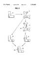
- FIG. 2illustrates a second preferred embodiment of the present invention.
- a feature 10 of binary mask designis again used to generate a mask design feature 12.
- This mask designis then used to generate feature 14 on a photomask and an aerial image 18 is generated from the image on the photomask.
- simulated image 30is generated as a simulated aerial image of mask design image 12.
- Aerial image 18is then compared to this simulated image 30 to obtain a comparison 32 where any incongruities 34 will appear as discrepancies between the two images.
- Image 30can also be the result of the convolution of feature 10 with some convolution function(s) representing, but not limited to, the aerial image, the mask fabrication process, OPC corrections, etc.
- the present inventioncan be used for x-ray masks, stencil masks for ion projection lithography, masks for electron beam projection lithography, etc.
- the techniques of the present inventioncan also be applied to imaging systems other than those used in the manufacture of integrated circuits.
- the inspection technique and aerial imagescould be performed out of focus in order to detect defects that mainly print out of focus such as phase defects.
- other techniques of mathematical processing of the datacan be used to generate images 20 and 30.
- the simulated image of the maskcan be generated during inspection or a portion of the simulation can be performed before inspection and the remainder during inspection. Accordingly, all changes or modifications which come within the meaning and range of equivalency of the claims are to be embraced within their scope.
Landscapes
- Physics & Mathematics (AREA)
- General Physics & Mathematics (AREA)
- Health & Medical Sciences (AREA)
- Life Sciences & Earth Sciences (AREA)
- Chemical & Material Sciences (AREA)
- Analytical Chemistry (AREA)
- Biochemistry (AREA)
- General Health & Medical Sciences (AREA)
- Immunology (AREA)
- Pathology (AREA)
- Preparing Plates And Mask In Photomechanical Process (AREA)
- Investigating Materials By The Use Of Optical Means Adapted For Particular Applications (AREA)
Abstract
Description
Claims (24)
Priority Applications (2)
| Application Number | Priority Date | Filing Date | Title |
|---|---|---|---|
| US08/696,652US5795688A (en) | 1996-08-14 | 1996-08-14 | Process for detecting defects in photomasks through aerial image comparisons |
| US10/810,406US20040179726A1 (en) | 1996-08-14 | 2004-03-26 | Process for detecting defects in photomasks |
Applications Claiming Priority (1)
| Application Number | Priority Date | Filing Date | Title |
|---|---|---|---|
| US08/696,652US5795688A (en) | 1996-08-14 | 1996-08-14 | Process for detecting defects in photomasks through aerial image comparisons |
Related Child Applications (1)
| Application Number | Title | Priority Date | Filing Date |
|---|---|---|---|
| US13511098ADivision | 1996-08-14 | 1998-08-17 |
Publications (1)
| Publication Number | Publication Date |
|---|---|
| US5795688Atrue US5795688A (en) | 1998-08-18 |
Family
ID=24797993
Family Applications (2)
| Application Number | Title | Priority Date | Filing Date |
|---|---|---|---|
| US08/696,652Expired - LifetimeUS5795688A (en) | 1996-08-14 | 1996-08-14 | Process for detecting defects in photomasks through aerial image comparisons |
| US10/810,406AbandonedUS20040179726A1 (en) | 1996-08-14 | 2004-03-26 | Process for detecting defects in photomasks |
Family Applications After (1)
| Application Number | Title | Priority Date | Filing Date |
|---|---|---|---|
| US10/810,406AbandonedUS20040179726A1 (en) | 1996-08-14 | 2004-03-26 | Process for detecting defects in photomasks |
Country Status (1)
| Country | Link |
|---|---|
| US (2) | US5795688A (en) |
Cited By (85)
| Publication number | Priority date | Publication date | Assignee | Title |
|---|---|---|---|---|
| WO1999014706A3 (en)* | 1997-09-17 | 1999-05-06 | Numerical Tech Inc | Visual inspection and verification system |
| US5965306A (en)* | 1997-10-15 | 1999-10-12 | International Business Machines Corporation | Method of determining the printability of photomask defects |
| US6016357A (en)* | 1997-06-16 | 2000-01-18 | International Business Machines Corporation | Feedback method to repair phase shift masks |
| US6078738A (en)* | 1997-05-08 | 2000-06-20 | Lsi Logic Corporation | Comparing aerial image to SEM of photoresist or substrate pattern for masking process characterization |
| US6120952A (en)* | 1998-10-01 | 2000-09-19 | Micron Technology, Inc. | Methods of reducing proximity effects in lithographic processes |
| US6183920B1 (en) | 1998-07-08 | 2001-02-06 | Matsushita Electric Industrial Co., Ltd. | Semiconductor device geometrical pattern correction process and geometrical pattern extraction process |
| WO2001013176A1 (en)* | 1999-08-02 | 2001-02-22 | Micron Technology, Inc. | Methods of determining alignment in the forming of phase shift regions in the fabrication of a phase shift mask |
| US6258493B1 (en) | 1996-09-18 | 2001-07-10 | Numerical Technologies, Inc. | Phase shifting circuit manufacture method and apparatus |
| US6261724B1 (en)* | 1999-06-16 | 2001-07-17 | International Business Machines Corporation | Method of modifying a microchip layout data set to generate a predicted mask printed data set |
| US6268093B1 (en) | 1999-10-13 | 2001-07-31 | Applied Materials, Inc. | Method for reticle inspection using aerial imaging |
| US6272018B1 (en) | 1999-02-11 | 2001-08-07 | Original Solutions Inc. | Method for the verification of the polarity and presence of components on a printed circuit board |
| US6317866B1 (en)* | 1997-08-19 | 2001-11-13 | Nec Corporation | Method of preparing charged particle beam drawing data and recording medium on which program thereof is recorded |
| US6329107B1 (en) | 2000-03-15 | 2001-12-11 | International Business Machines Corporation | Method of characterizing partial coherent light illumination and its application to serif mask design |
| US6343370B1 (en)* | 1997-12-05 | 2002-01-29 | Mitsubishi Denki Kabusiki Kaisha | Apparatus and process for pattern distortion detection for semiconductor process and semiconductor device manufactured by use of the apparatus or process |
| US20020035461A1 (en)* | 1997-09-17 | 2002-03-21 | Numerical Technologies, Inc. | Visual analysis and verification system using advanced tools |
| WO2001065317A3 (en)* | 2000-02-29 | 2002-03-28 | Advanced Micro Devices Inc | Method for evaluation of reticle image using aerial image simulator |
| US6370679B1 (en) | 1997-09-17 | 2002-04-09 | Numerical Technologies, Inc. | Data hierarchy layout correction and verification method and apparatus |
| US6373975B1 (en) | 1999-01-25 | 2002-04-16 | International Business Machines Corporation | Error checking of simulated printed images with process window effects included |
| US6393604B1 (en)* | 1998-11-09 | 2002-05-21 | Nec Corporation | Process for preparing data for direct-writing by a charged particle ray, process for verifying data for direct-writing by a charged particle ray, process for displaying data for direct-writing by a charged particle ray, and exposure device |
| US6400838B2 (en)* | 1997-07-29 | 2002-06-04 | Kabushiki Kaisha Toshiba | Pattern inspection equipment, pattern inspection method, and storage medium storing pattern inspection program |
| US6406818B1 (en)* | 1999-03-31 | 2002-06-18 | Photronics, Inc. | Method of manufacturing photomasks by plasma etching with resist stripped |
| US6425112B1 (en) | 1999-06-17 | 2002-07-23 | International Business Machines Corporation | Auto correction of error checked simulated printed images |
| US6440612B1 (en) | 1999-09-01 | 2002-08-27 | Micron Technology, Inc. | Field correction of overlay error |
| US6451490B1 (en) | 2000-11-08 | 2002-09-17 | International Business Machines Corporation | Method to overcome image shortening by use of sub-resolution reticle features |
| US6453457B1 (en) | 2000-09-29 | 2002-09-17 | Numerical Technologies, Inc. | Selection of evaluation point locations based on proximity effects model amplitudes for correcting proximity effects in a fabrication layout |
| US6453452B1 (en) | 1997-12-12 | 2002-09-17 | Numerical Technologies, Inc. | Method and apparatus for data hierarchy maintenance in a system for mask description |
| US6466315B1 (en) | 1999-09-03 | 2002-10-15 | Applied Materials, Inc. | Method and system for reticle inspection by photolithography simulation |
| US6470489B1 (en) | 1997-09-17 | 2002-10-22 | Numerical Technologies, Inc. | Design rule checking system and method |
| US6483937B1 (en)* | 1999-06-17 | 2002-11-19 | International Business Machines Corporation | Process for inspecting an object |
| US6485870B1 (en)* | 1999-09-21 | 2002-11-26 | Nikon Corporation | Charged-particle-beam microlithography masks and methods for manufacturing same |
| US20030044059A1 (en)* | 2001-08-28 | 2003-03-06 | Numerical Technologies, Inc. | System and method for indentifying dummy features on a mask layer |
| US6539521B1 (en) | 2000-09-29 | 2003-03-25 | Numerical Technologies, Inc. | Dissection of corners in a fabrication layout for correcting proximity effects |
| US20030082463A1 (en)* | 2001-10-09 | 2003-05-01 | Thomas Laidig | Method of two dimensional feature model calibration and optimization |
| WO2002075793A3 (en)* | 2001-03-20 | 2003-05-01 | Numerial Technologies Inc | System and method of providing mask defect printability analysis |
| US6560766B2 (en) | 2001-07-26 | 2003-05-06 | Numerical Technologies, Inc. | Method and apparatus for analyzing a layout using an instance-based representation |
| US20030093251A1 (en)* | 2001-11-14 | 2003-05-15 | Numerical Technologies, Inc. | Simulation using design geometry information |
| US6578190B2 (en)* | 2001-01-11 | 2003-06-10 | International Business Machines Corporation | Process window based optical proximity correction of lithographic images |
| US6578188B1 (en) | 1997-09-17 | 2003-06-10 | Numerical Technologies, Inc. | Method and apparatus for a network-based mask defect printability analysis system |
| US20030128870A1 (en)* | 2002-01-08 | 2003-07-10 | Pease R. Fabian W. | System and method for aerial image sensing |
| US6625800B1 (en)* | 1999-12-30 | 2003-09-23 | Intel Corporation | Method and apparatus for physical image based inspection system |
| US6625801B1 (en) | 2000-09-29 | 2003-09-23 | Numerical Technologies, Inc. | Dissection of printed edges from a fabrication layout for correcting proximity effects |
| US20030181139A1 (en)* | 2002-02-04 | 2003-09-25 | Kurt Lehman | Windows configurable to be coupled to a process tool or to be disposed within an opening in a polishing pad |
| US6631307B1 (en)* | 1998-03-19 | 2003-10-07 | Taiwan Semiconductor Manufacturing Company | Use of logical operations in place of OPC software |
| US20030192567A1 (en)* | 2002-04-12 | 2003-10-16 | Yoshihiro Koizumi | Method of making foreign matter harmless |
| US20030219154A1 (en)* | 2002-05-22 | 2003-11-27 | Medvedeva Marina M. | Quality measurement of an aerial image |
| US6658641B2 (en)* | 2000-10-18 | 2003-12-02 | Isao Ashida | Method for mask data verification and computer readable record medium recording the verification program |
| US20030226951A1 (en)* | 2002-06-07 | 2003-12-11 | Jun Ye | System and method for lithography process monitoring and control |
| US6665856B1 (en) | 2000-12-01 | 2003-12-16 | Numerical Technologies, Inc. | Displacing edge segments on a fabrication layout based on proximity effects model amplitudes for correcting proximity effects |
| US6670082B2 (en) | 2001-10-09 | 2003-12-30 | Numerical Technologies, Inc. | System and method for correcting 3D effects in an alternating phase-shifting mask |
| US20040008879A1 (en)* | 2002-07-11 | 2004-01-15 | United Microelectronics Corp. | Method for detecting wafer level defect |
| US20040015808A1 (en)* | 1997-09-17 | 2004-01-22 | Numerical Technologies, Inc. | System and method for providing defect printability analysis of photolithographic masks with job-based automation |
| WO2002099533A3 (en)* | 2001-06-07 | 2004-02-12 | Applied Materials Inc | Alternating phase-shift mask inspection method and apparatus |
| US6704695B1 (en) | 1999-07-16 | 2004-03-09 | International Business Machines Corporation | Interactive optical proximity correction design method |
| US20040052411A1 (en)* | 2002-09-13 | 2004-03-18 | Numerical Technologies, Inc. | Soft defect printability simulation and analysis for masks |
| US20040066963A1 (en)* | 2002-08-06 | 2004-04-08 | Christoph Hechtl | Method of inspecting a mask |
| US6721928B2 (en) | 2001-07-26 | 2004-04-13 | Numerical Technologies, Inc. | Verification utilizing instance-based hierarchy management |
| US20040098216A1 (en)* | 2002-11-04 | 2004-05-20 | Jun Ye | Method and apparatus for monitoring integrated circuit fabrication |
| US20040119957A1 (en)* | 2002-12-19 | 2004-06-24 | Renwick Stephen P. | Method to diagnose imperfections in illuminator of a lithographic tool |
| US20040151991A1 (en)* | 2002-09-18 | 2004-08-05 | Stewart Diane K. | Photolithography mask repair |
| US20040165761A1 (en)* | 2003-02-26 | 2004-08-26 | Chang-Cheng Hung | System and method for inspecting errors on a wafer |
| US6792590B1 (en) | 2000-09-29 | 2004-09-14 | Numerical Technologies, Inc. | Dissection of edges with projection points in a fabrication layout for correcting proximity effects |
| US20040179726A1 (en)* | 1996-08-14 | 2004-09-16 | James Burdorf | Process for detecting defects in photomasks |
| US6873720B2 (en) | 2001-03-20 | 2005-03-29 | Synopsys, Inc. | System and method of providing mask defect printability analysis |
| US20050096888A1 (en)* | 2001-05-11 | 2005-05-05 | Ismail Yehea I. | Efficient model order reduction via multi-point moment matching |
| US20050149902A1 (en)* | 2003-11-05 | 2005-07-07 | Xuelong Shi | Eigen decomposition based OPC model |
| US6925202B2 (en) | 2001-03-20 | 2005-08-02 | Synopsys, Inc. | System and method of providing mask quality control |
| US20050177772A1 (en)* | 2004-01-28 | 2005-08-11 | Microsoft Corporation | Method and system for masking dynamic regions in a user interface to enable testing of user interface consistency |
| US20050179886A1 (en)* | 2004-01-30 | 2005-08-18 | Xuelong Shi | Method of predicting and minimizing model OPC deviation due to mix/match of exposure tools using a calibrated eigen decomposition model |
| US20050210437A1 (en)* | 2004-01-30 | 2005-09-22 | Xuelong Shi | Method of manufacturing reliability checking and verification for lithography process using a calibrated eigen decomposition model |
| US20060080633A1 (en)* | 2004-09-14 | 2006-04-13 | Michael Hsu | Method for performing full-chip manufacturing reliability checking and correction |
| US20060099519A1 (en)* | 2004-11-10 | 2006-05-11 | Moriarty Michael H | Method of depositing a material providing a specified attenuation and phase shift |
| US7053355B2 (en) | 2003-03-18 | 2006-05-30 | Brion Technologies, Inc. | System and method for lithography process monitoring and control |
| DE102005009536A1 (en)* | 2005-02-25 | 2006-08-31 | Carl Zeiss Sms Gmbh | Process to inspect masks for weak spots uses aerial image simulation to produce a list of critical points or hotspots, which is analyzed using Aerial Imaging Measurement system to compare real with simulated images |
| US20060222963A1 (en)* | 2005-04-01 | 2006-10-05 | Terhune Robert V | Methods of forming patterns in substrates |
| US20060242619A1 (en)* | 1997-09-17 | 2006-10-26 | Synopsys, Inc. | System And Method For Providing Defect Printability Analysis Of Photolithographic Masks With Job-Based Automation |
| US20070002311A1 (en)* | 2004-08-26 | 2007-01-04 | Asml Masktools B.V. | Method of performing resist process calibration/optimization and DOE optimization for providing OPE matching between different lithography systems |
| US20070157154A1 (en)* | 2005-12-29 | 2007-07-05 | Robert John Socha | Method, program product and apparatus for model based geometry decomposition for use in a multiple exposure process |
| WO2007088542A2 (en) | 2006-02-01 | 2007-08-09 | Applied Materials Israel Limited | Method and system for evaluating a variation in a parameter of a pattern |
| US20080152212A1 (en)* | 2004-08-27 | 2008-06-26 | Haim Feldman | Simulation of aerial images |
| US20090262317A1 (en)* | 2008-04-18 | 2009-10-22 | International Business Machines Corporation | Test method for determining reticle transmission stability |
| US20090304262A1 (en)* | 2008-06-06 | 2009-12-10 | Advanced Mask Inspection Technology, Inc. | Ultrafine pattern discrimination using transmitted/reflected workpiece images for use in lithography inspection system |
| US8124300B1 (en)* | 2004-11-30 | 2012-02-28 | Globalfoundries Inc. | Method of lithographic mask correction using localized transmission adjustment |
| US20150324963A1 (en)* | 2014-05-06 | 2015-11-12 | Kla-Tencor Corporation | Reticle Inspection Using Near-Field Recovery |
| US10216890B2 (en) | 2004-04-21 | 2019-02-26 | Iym Technologies Llc | Integrated circuits having in-situ constraints |
| US10395361B2 (en) | 2015-08-10 | 2019-08-27 | Kla-Tencor Corporation | Apparatus and methods for inspecting reticles |
Families Citing this family (9)
| Publication number | Priority date | Publication date | Assignee | Title |
|---|---|---|---|---|
| JP4266971B2 (en)* | 2005-09-22 | 2009-05-27 | アドバンスド・マスク・インスペクション・テクノロジー株式会社 | Pattern inspection apparatus, pattern inspection method, and inspection target sample |
| CN1884043B (en)* | 2006-07-07 | 2011-05-11 | 南京大学 | Graphics compensation method for electron beam direct-writing graphics in preparation of nano dot structure |
| DE102006043874B4 (en)* | 2006-09-15 | 2020-07-09 | Carl Zeiss Smt Gmbh | Method and device for repairing photolithography masks |
| TWI644169B (en)* | 2014-05-06 | 2018-12-11 | 美商克萊譚克公司 | Computer-implemented method, non-transitory computer-readable medium, and system for reticle inspection using near-field recovery |
| JP6307367B2 (en) | 2014-06-26 | 2018-04-04 | 株式会社ニューフレアテクノロジー | Mask inspection apparatus, mask evaluation method and mask evaluation system |
| KR20240169729A (en) | 2015-08-10 | 2024-12-03 | 케이엘에이 코포레이션 | Apparatus and methods for predicting wafer-level defect printability |
| US10964014B2 (en)* | 2017-10-30 | 2021-03-30 | Taiwan Semiconductor Manufacturing Company, Ltd. | Defect detecting method and defect detecting system |
| US12400314B2 (en)* | 2021-09-13 | 2025-08-26 | Applied Materials Israel Ltd. | Mask inspection for semiconductor specimen fabrication |
| US20250112052A1 (en)* | 2023-09-29 | 2025-04-03 | Applied Materials, Inc. | Directional rie feature rectangularity |
Citations (3)
| Publication number | Priority date | Publication date | Assignee | Title |
|---|---|---|---|---|
| EP0138639A2 (en)* | 1983-09-16 | 1985-04-24 | Fujitsu Limited | Inspection method for mask pattern used in semiconductor device fabrication |
| US4809341A (en)* | 1986-07-18 | 1989-02-28 | Fujitsu Limited | Test method and apparatus for a reticle or mask pattern used in semiconductor device fabrication |
| US5481624A (en)* | 1992-04-27 | 1996-01-02 | Mitsubishi Denki Kabushiki Kaisha | Mask inspecting method and mask detector |
Family Cites Families (23)
| Publication number | Priority date | Publication date | Assignee | Title |
|---|---|---|---|---|
| JPS5832147A (en)* | 1981-08-20 | 1983-02-25 | Fujitsu Ltd | Reticle inspection method |
| US4926489A (en)* | 1983-03-11 | 1990-05-15 | Kla Instruments Corporation | Reticle inspection system |
| JPH0750664B2 (en)* | 1983-06-23 | 1995-05-31 | 富士通株式会社 | Reticle inspection method |
| US4644172A (en)* | 1984-02-22 | 1987-02-17 | Kla Instruments Corporation | Electronic control of an automatic wafer inspection system |
| US4633504A (en)* | 1984-06-28 | 1986-12-30 | Kla Instruments Corporation | Automatic photomask inspection system having image enhancement means |
| DE3587582D1 (en)* | 1985-03-14 | 1993-10-21 | Beltronics Inc | Device and method for automatically inspecting objects and for identifying or recognizing known and unknown parts thereof, including errors and the like. |
| US5029222A (en)* | 1987-09-02 | 1991-07-02 | Fujitsu Limited | Photoelectron image projection apparatus |
| JP2710967B2 (en)* | 1988-11-22 | 1998-02-10 | 株式会社日立製作所 | Manufacturing method of integrated circuit device |
| JPH0341347A (en)* | 1989-04-13 | 1991-02-21 | Mitsubishi Rayon Co Ltd | Inspection of defect and apparatus therefor |
| US5129009A (en)* | 1990-06-04 | 1992-07-07 | Motorola, Inc. | Method for automatic semiconductor wafer inspection |
| JP2747105B2 (en)* | 1990-11-05 | 1998-05-06 | 富士通株式会社 | Image data verification method and apparatus |
| US5563702A (en)* | 1991-08-22 | 1996-10-08 | Kla Instruments Corporation | Automated photomask inspection apparatus and method |
| US5475766A (en)* | 1991-09-05 | 1995-12-12 | Kabushiki Kaisha Toshiba | Pattern inspection apparatus with corner rounding of reference pattern data |
| JP3154802B2 (en)* | 1992-03-31 | 2001-04-09 | 株式会社東芝 | Pattern defect inspection equipment |
| JP3328323B2 (en)* | 1992-07-20 | 2002-09-24 | 株式会社日立製作所 | Method for manufacturing phase shift mask and method for manufacturing semiconductor integrated circuit device |
| US5307421A (en)* | 1992-10-14 | 1994-04-26 | Commissariat A L'energie Atomique | Process for producing a synthesized reference image for the inspection of objects and apparatus for performing the same |
| JPH0915833A (en)* | 1995-06-30 | 1997-01-17 | Sony Corp | Scanning data forming device and scanning data forming method in exposing mask manufacturing device |
| US6064484A (en)* | 1996-03-13 | 2000-05-16 | Fujitsu Limited | Pattern inspection method and system |
| US5862058A (en)* | 1996-05-16 | 1999-01-19 | International Business Machines Corporation | Optical proximity correction method and system |
| US5707765A (en)* | 1996-05-28 | 1998-01-13 | Microunity Systems Engineering, Inc. | Photolithography mask using serifs and method thereof |
| US5849440A (en)* | 1996-07-02 | 1998-12-15 | Motorola, Inc. | Process for producing and inspecting a lithographic reticle and fabricating semiconductor devices using same |
| US5795688A (en)* | 1996-08-14 | 1998-08-18 | Micron Technology, Inc. | Process for detecting defects in photomasks through aerial image comparisons |
| US5804340A (en)* | 1996-12-23 | 1998-09-08 | Lsi Logic Corporation | Photomask inspection method and inspection tape therefor |
- 1996
- 1996-08-14USUS08/696,652patent/US5795688A/ennot_activeExpired - Lifetime
- 2004
- 2004-03-26USUS10/810,406patent/US20040179726A1/ennot_activeAbandoned
Patent Citations (3)
| Publication number | Priority date | Publication date | Assignee | Title |
|---|---|---|---|---|
| EP0138639A2 (en)* | 1983-09-16 | 1985-04-24 | Fujitsu Limited | Inspection method for mask pattern used in semiconductor device fabrication |
| US4809341A (en)* | 1986-07-18 | 1989-02-28 | Fujitsu Limited | Test method and apparatus for a reticle or mask pattern used in semiconductor device fabrication |
| US5481624A (en)* | 1992-04-27 | 1996-01-02 | Mitsubishi Denki Kabushiki Kaisha | Mask inspecting method and mask detector |
Cited By (206)
| Publication number | Priority date | Publication date | Assignee | Title |
|---|---|---|---|---|
| US20040179726A1 (en)* | 1996-08-14 | 2004-09-16 | James Burdorf | Process for detecting defects in photomasks |
| US6566023B2 (en) | 1996-09-18 | 2003-05-20 | Numerical Technology, Inc. | Phase shifting circuit manufacture method and apparatus |
| US6818385B2 (en) | 1996-09-18 | 2004-11-16 | Numerical Technologies, Inc. | Phase shifting circuit manufacture method and apparatus |
| US6436590B2 (en) | 1996-09-18 | 2002-08-20 | Numerical Technologies, Inc. | Phase shifting circuit manufacture method and apparatus |
| US6258493B1 (en) | 1996-09-18 | 2001-07-10 | Numerical Technologies, Inc. | Phase shifting circuit manufacture method and apparatus |
| US6420074B2 (en) | 1996-09-18 | 2002-07-16 | Numerial Technologies, Inc. | Phase shifting circuit manufacture method and apparatus |
| US6078738A (en)* | 1997-05-08 | 2000-06-20 | Lsi Logic Corporation | Comparing aerial image to SEM of photoresist or substrate pattern for masking process characterization |
| US6081659A (en)* | 1997-05-08 | 2000-06-27 | Lsi Logic Corporation | Comparing aerial image to actual photoresist pattern for masking process characterization |
| US6016357A (en)* | 1997-06-16 | 2000-01-18 | International Business Machines Corporation | Feedback method to repair phase shift masks |
| US6400838B2 (en)* | 1997-07-29 | 2002-06-04 | Kabushiki Kaisha Toshiba | Pattern inspection equipment, pattern inspection method, and storage medium storing pattern inspection program |
| US6317866B1 (en)* | 1997-08-19 | 2001-11-13 | Nec Corporation | Method of preparing charged particle beam drawing data and recording medium on which program thereof is recorded |
| US7093229B2 (en) | 1997-09-17 | 2006-08-15 | Synopsys, Inc. | System and method for providing defect printability analysis of photolithographic masks with job-based automation |
| US7356788B2 (en) | 1997-09-17 | 2008-04-08 | Synopsys, Inc. | Method and apparatus for data hierarchy maintenance in a system for mask description |
| US20030018948A1 (en)* | 1997-09-17 | 2003-01-23 | Numerical Technologies, Inc. | Method and apparatus for data hierarchy maintenance in a system for mask description |
| US7107571B2 (en) | 1997-09-17 | 2006-09-12 | Synopsys, Inc. | Visual analysis and verification system using advanced tools |
| US6470489B1 (en) | 1997-09-17 | 2002-10-22 | Numerical Technologies, Inc. | Design rule checking system and method |
| US7523027B2 (en)* | 1997-09-17 | 2009-04-21 | Synopsys, Inc. | Visual inspection and verification system |
| US20060242619A1 (en)* | 1997-09-17 | 2006-10-26 | Synopsys, Inc. | System And Method For Providing Defect Printability Analysis Of Photolithographic Masks With Job-Based Automation |
| US20020019729A1 (en)* | 1997-09-17 | 2002-02-14 | Numerical Technologies, Inc. | Visual inspection and verification system |
| US20020035461A1 (en)* | 1997-09-17 | 2002-03-21 | Numerical Technologies, Inc. | Visual analysis and verification system using advanced tools |
| US20040243320A1 (en)* | 1997-09-17 | 2004-12-02 | Numerical Technologies, Inc. | Visual inspection and verification system |
| US6370679B1 (en) | 1997-09-17 | 2002-04-09 | Numerical Technologies, Inc. | Data hierarchy layout correction and verification method and apparatus |
| US7003755B2 (en) | 1997-09-17 | 2006-02-21 | Synopsys Inc. | User interface for a networked-based mask defect printability analysis system |
| US6757645B2 (en)* | 1997-09-17 | 2004-06-29 | Numerical Technologies, Inc. | Visual inspection and verification system |
| US20040015808A1 (en)* | 1997-09-17 | 2004-01-22 | Numerical Technologies, Inc. | System and method for providing defect printability analysis of photolithographic masks with job-based automation |
| WO1999014706A3 (en)* | 1997-09-17 | 1999-05-06 | Numerical Tech Inc | Visual inspection and verification system |
| US7617474B2 (en) | 1997-09-17 | 2009-11-10 | Synopsys, Inc. | System and method for providing defect printability analysis of photolithographic masks with job-based automation |
| US20030126581A1 (en)* | 1997-09-17 | 2003-07-03 | Numerical Technologies, Inc. | User interface for a network-based mask defect printability analysis system |
| US6578188B1 (en) | 1997-09-17 | 2003-06-10 | Numerical Technologies, Inc. | Method and apparatus for a network-based mask defect printability analysis system |
| US5965306A (en)* | 1997-10-15 | 1999-10-12 | International Business Machines Corporation | Method of determining the printability of photomask defects |
| US6343370B1 (en)* | 1997-12-05 | 2002-01-29 | Mitsubishi Denki Kabusiki Kaisha | Apparatus and process for pattern distortion detection for semiconductor process and semiconductor device manufactured by use of the apparatus or process |
| US6453452B1 (en) | 1997-12-12 | 2002-09-17 | Numerical Technologies, Inc. | Method and apparatus for data hierarchy maintenance in a system for mask description |
| US6631307B1 (en)* | 1998-03-19 | 2003-10-07 | Taiwan Semiconductor Manufacturing Company | Use of logical operations in place of OPC software |
| US6183920B1 (en) | 1998-07-08 | 2001-02-06 | Matsushita Electric Industrial Co., Ltd. | Semiconductor device geometrical pattern correction process and geometrical pattern extraction process |
| US6319644B2 (en) | 1998-10-01 | 2001-11-20 | Micron Technology, Inc. | Methods of reducing proximity effects in lithographic processes |
| US6284419B2 (en) | 1998-10-01 | 2001-09-04 | Micron Technology, Inc. | Methods of reducing proximity effects in lithographic processes |
| US6120952A (en)* | 1998-10-01 | 2000-09-19 | Micron Technology, Inc. | Methods of reducing proximity effects in lithographic processes |
| US6393604B1 (en)* | 1998-11-09 | 2002-05-21 | Nec Corporation | Process for preparing data for direct-writing by a charged particle ray, process for verifying data for direct-writing by a charged particle ray, process for displaying data for direct-writing by a charged particle ray, and exposure device |
| US6373975B1 (en) | 1999-01-25 | 2002-04-16 | International Business Machines Corporation | Error checking of simulated printed images with process window effects included |
| US6480394B1 (en) | 1999-02-11 | 2002-11-12 | Original Solutions Inc. | Method for the verification of the polarity, presence, alignment of components and short circuits on a printed circuits board |
| US6272018B1 (en) | 1999-02-11 | 2001-08-07 | Original Solutions Inc. | Method for the verification of the polarity and presence of components on a printed circuit board |
| US6562549B2 (en) | 1999-03-31 | 2003-05-13 | Photronics, Inc. | Method of manufacturing photomasks by plasma etching with resist stripped |
| US6406818B1 (en)* | 1999-03-31 | 2002-06-18 | Photronics, Inc. | Method of manufacturing photomasks by plasma etching with resist stripped |
| US6261724B1 (en)* | 1999-06-16 | 2001-07-17 | International Business Machines Corporation | Method of modifying a microchip layout data set to generate a predicted mask printed data set |
| US6483937B1 (en)* | 1999-06-17 | 2002-11-19 | International Business Machines Corporation | Process for inspecting an object |
| US6425112B1 (en) | 1999-06-17 | 2002-07-23 | International Business Machines Corporation | Auto correction of error checked simulated printed images |
| US6704695B1 (en) | 1999-07-16 | 2004-03-09 | International Business Machines Corporation | Interactive optical proximity correction design method |
| WO2001013176A1 (en)* | 1999-08-02 | 2001-02-22 | Micron Technology, Inc. | Methods of determining alignment in the forming of phase shift regions in the fabrication of a phase shift mask |
| US6395432B1 (en) | 1999-08-02 | 2002-05-28 | Micron Technology, Inc. | Methods of determining processing alignment in the forming of phase shift regions |
| US6811934B2 (en) | 1999-09-01 | 2004-11-02 | Micron Technology, Inc. | Field correction of overlay error |
| US6440612B1 (en) | 1999-09-01 | 2002-08-27 | Micron Technology, Inc. | Field correction of overlay error |
| US6779171B2 (en) | 1999-09-01 | 2004-08-17 | Micron Technology, Inc. | Field correction of overlay error |
| US6841889B2 (en) | 1999-09-01 | 2005-01-11 | Micron Technology, Inc. | Field correction of overlay error |
| US6893786B2 (en) | 1999-09-01 | 2005-05-17 | Micron Technology, Inc. | Field correction of overlay error |
| US6466315B1 (en) | 1999-09-03 | 2002-10-15 | Applied Materials, Inc. | Method and system for reticle inspection by photolithography simulation |
| US6485870B1 (en)* | 1999-09-21 | 2002-11-26 | Nikon Corporation | Charged-particle-beam microlithography masks and methods for manufacturing same |
| US7133548B2 (en) | 1999-10-13 | 2006-11-07 | Applied Materials, Inc. | Method and apparatus for reticle inspection using aerial imaging |
| US6268093B1 (en) | 1999-10-13 | 2001-07-31 | Applied Materials, Inc. | Method for reticle inspection using aerial imaging |
| US20010019625A1 (en)* | 1999-10-13 | 2001-09-06 | Boaz Kenan | Method and apparatus for reticle inspection using aerial imaging |
| US6625800B1 (en)* | 1999-12-30 | 2003-09-23 | Intel Corporation | Method and apparatus for physical image based inspection system |
| JP2003525529A (en)* | 2000-02-29 | 2003-08-26 | アドバンスト・マイクロ・ディバイシズ・インコーポレイテッド | A method for evaluating a reticle image using an optical image simulator |
| WO2001065317A3 (en)* | 2000-02-29 | 2002-03-28 | Advanced Micro Devices Inc | Method for evaluation of reticle image using aerial image simulator |
| US7120285B1 (en) | 2000-02-29 | 2006-10-10 | Advanced Micro Devices, Inc. | Method for evaluation of reticle image using aerial image simulator |
| KR100734533B1 (en)* | 2000-02-29 | 2007-07-04 | 어드밴스드 마이크로 디바이시즈, 인코포레이티드 | Evaluation Method of Reticle Images Using Aerial Image Simulator |
| US6329107B1 (en) | 2000-03-15 | 2001-12-11 | International Business Machines Corporation | Method of characterizing partial coherent light illumination and its application to serif mask design |
| US6918104B2 (en) | 2000-09-29 | 2005-07-12 | Synopsys, Inc. | Dissection of printed edges from a fabrication layout for correcting proximity effects |
| US6792590B1 (en) | 2000-09-29 | 2004-09-14 | Numerical Technologies, Inc. | Dissection of edges with projection points in a fabrication layout for correcting proximity effects |
| US6453457B1 (en) | 2000-09-29 | 2002-09-17 | Numerical Technologies, Inc. | Selection of evaluation point locations based on proximity effects model amplitudes for correcting proximity effects in a fabrication layout |
| US6539521B1 (en) | 2000-09-29 | 2003-03-25 | Numerical Technologies, Inc. | Dissection of corners in a fabrication layout for correcting proximity effects |
| US20040221255A1 (en)* | 2000-09-29 | 2004-11-04 | Numerical Technologies, Inc. | Dissection of edges with projection points in a fabrication layout for correcting proximity effects |
| US6625801B1 (en) | 2000-09-29 | 2003-09-23 | Numerical Technologies, Inc. | Dissection of printed edges from a fabrication layout for correcting proximity effects |
| US7003757B2 (en) | 2000-09-29 | 2006-02-21 | Synopsys, Inc. | Dissection of edges with projection points in a fabrication layout for correcting proximity effects |
| US6658641B2 (en)* | 2000-10-18 | 2003-12-02 | Isao Ashida | Method for mask data verification and computer readable record medium recording the verification program |
| US6451490B1 (en) | 2000-11-08 | 2002-09-17 | International Business Machines Corporation | Method to overcome image shortening by use of sub-resolution reticle features |
| US6665856B1 (en) | 2000-12-01 | 2003-12-16 | Numerical Technologies, Inc. | Displacing edge segments on a fabrication layout based on proximity effects model amplitudes for correcting proximity effects |
| US6578190B2 (en)* | 2001-01-11 | 2003-06-10 | International Business Machines Corporation | Process window based optical proximity correction of lithographic images |
| US7254251B2 (en) | 2001-03-20 | 2007-08-07 | Synopsys, Inc. | System and method of providing mask defect printability analysis |
| US6925202B2 (en) | 2001-03-20 | 2005-08-02 | Synopsys, Inc. | System and method of providing mask quality control |
| US20050190957A1 (en)* | 2001-03-20 | 2005-09-01 | Synopsys, Inc. | System and method of providing mask defect printability analysis |
| US6873720B2 (en) | 2001-03-20 | 2005-03-29 | Synopsys, Inc. | System and method of providing mask defect printability analysis |
| US7403649B2 (en) | 2001-03-20 | 2008-07-22 | Synopsys, Inc. | System and method of providing mask defect printability analysis |
| WO2002075793A3 (en)* | 2001-03-20 | 2003-05-01 | Numerial Technologies Inc | System and method of providing mask defect printability analysis |
| US20080260235A1 (en)* | 2001-03-20 | 2008-10-23 | Synopsys, Inc. | System And Method Of Providing Mask Defect Printability Analysis |
| US7565001B2 (en) | 2001-03-20 | 2009-07-21 | Synopsys, Inc. | System and method of providing mask defect printability analysis |
| US20090245621A1 (en)* | 2001-03-20 | 2009-10-01 | Synopsys, Inc, | System And Method Of Providing Mask Defect Printability Analysis |
| US7835565B2 (en) | 2001-03-20 | 2010-11-16 | Synopsys, Inc. | System and method of providing mask defect printability analysis |
| US20050096888A1 (en)* | 2001-05-11 | 2005-05-05 | Ismail Yehea I. | Efficient model order reduction via multi-point moment matching |
| WO2002099533A3 (en)* | 2001-06-07 | 2004-02-12 | Applied Materials Inc | Alternating phase-shift mask inspection method and apparatus |
| US7072502B2 (en) | 2001-06-07 | 2006-07-04 | Applied Materials, Inc. | Alternating phase-shift mask inspection method and apparatus |
| US6560766B2 (en) | 2001-07-26 | 2003-05-06 | Numerical Technologies, Inc. | Method and apparatus for analyzing a layout using an instance-based representation |
| US6721928B2 (en) | 2001-07-26 | 2004-04-13 | Numerical Technologies, Inc. | Verification utilizing instance-based hierarchy management |
| US7014955B2 (en) | 2001-08-28 | 2006-03-21 | Synopsys, Inc. | System and method for indentifying dummy features on a mask layer |
| US20030044059A1 (en)* | 2001-08-28 | 2003-03-06 | Numerical Technologies, Inc. | System and method for indentifying dummy features on a mask layer |
| US7820341B2 (en) | 2001-10-09 | 2010-10-26 | Asml Masktools B. V. | Method of two dimensional feature model calibration and optimization |
| US20030082463A1 (en)* | 2001-10-09 | 2003-05-01 | Thomas Laidig | Method of two dimensional feature model calibration and optimization |
| US6670082B2 (en) | 2001-10-09 | 2003-12-30 | Numerical Technologies, Inc. | System and method for correcting 3D effects in an alternating phase-shifting mask |
| US7175940B2 (en) | 2001-10-09 | 2007-02-13 | Asml Masktools B.V. | Method of two dimensional feature model calibration and optimization |
| US20070117030A1 (en)* | 2001-10-09 | 2007-05-24 | Asml Masktools B. V. | Method of two dimensional feature model calibration and optimization |
| US20040076895A1 (en)* | 2001-10-09 | 2004-04-22 | Numerical Technologies, Inc. | System and method for correcting 3D effects in an alternating phase-shifting mask |
| US6830854B2 (en) | 2001-10-09 | 2004-12-14 | Numerical Technologies, Inc. | System and method for correcting 3D effects in an alternating phase-shifting mask |
| US6976240B2 (en) | 2001-11-14 | 2005-12-13 | Synopsys Inc. | Simulation using design geometry information |
| US20030093251A1 (en)* | 2001-11-14 | 2003-05-15 | Numerical Technologies, Inc. | Simulation using design geometry information |
| US20030128870A1 (en)* | 2002-01-08 | 2003-07-10 | Pease R. Fabian W. | System and method for aerial image sensing |
| US6906305B2 (en) | 2002-01-08 | 2005-06-14 | Brion Technologies, Inc. | System and method for aerial image sensing |
| US6884146B2 (en) | 2002-02-04 | 2005-04-26 | Kla-Tencor Technologies Corp. | Systems and methods for characterizing a polishing process |
| US20030181138A1 (en)* | 2002-02-04 | 2003-09-25 | Kurt Lehman | Methods and systems for determining a characteristic of polishing within a zone on a specimen from combined output signals of an eddy current device |
| US8831767B2 (en) | 2002-02-04 | 2014-09-09 | Kla-Tencor Technologies Corp. | Methods and systems for monitoring a parameter of a measurement device during polishing, damage to a specimen during polishing, or a characteristic of a polishing pad or tool |
| US8010222B2 (en) | 2002-02-04 | 2011-08-30 | Kla-Tencor Technologies Corp. | Methods and systems for monitoring a parameter of a measurement device during polishing, damage to a specimen during polishing, or a characteristic of a polishing pad or tool |
| US20030181139A1 (en)* | 2002-02-04 | 2003-09-25 | Kurt Lehman | Windows configurable to be coupled to a process tool or to be disposed within an opening in a polishing pad |
| US6866559B2 (en) | 2002-02-04 | 2005-03-15 | Kla-Tencor Technologies | Windows configurable to be coupled to a process tool or to be disposed within an opening in a polishing pad |
| US20030180973A1 (en)* | 2002-02-04 | 2003-09-25 | Kurt Lehman | Methods and systems for monitoring a parameter of a measurement device during polishing, damage to a specimen during polishing, or a characteristic of a polishing pad or tool |
| US20060131273A1 (en)* | 2002-02-04 | 2006-06-22 | Kla-Tencor Technologies Corp. | Methods and systems for monitoring a parameter of a measurement device during polishing, damage to a specimen during polishing, or a characteristic of a polishing pad or tool |
| US20060148383A1 (en)* | 2002-02-04 | 2006-07-06 | Kla Tencor Technologies | Methods and systems for detecting a presence of blobs on a specimen during a polishing process |
| US7332438B2 (en) | 2002-02-04 | 2008-02-19 | Kla-Tencor Technologies Corp. | Methods and systems for monitoring a parameter of a measurement device during polishing, damage to a specimen during polishing, or a characteristic of a polishing pad or tool |
| US20030190864A1 (en)* | 2002-02-04 | 2003-10-09 | Kurt Lehman | Methods and systems for detecting a presence of blobs on a specimen during a polishing process |
| US6935922B2 (en) | 2002-02-04 | 2005-08-30 | Kla-Tencor Technologies Corp. | Methods and systems for generating a two-dimensional map of a characteristic at relative or absolute locations of measurement spots on a specimen during polishing |
| US7175503B2 (en) | 2002-02-04 | 2007-02-13 | Kla-Tencor Technologies Corp. | Methods and systems for determining a characteristic of polishing within a zone on a specimen from combined output signals of an eddy current device |
| US7030018B2 (en) | 2002-02-04 | 2006-04-18 | Kla-Tencor Technologies Corp. | Methods and systems for monitoring a parameter of a measurement device during polishing, damage to a specimen during polishing, or a characteristic of a polishing pad or tool |
| US7052369B2 (en) | 2002-02-04 | 2006-05-30 | Kla-Tencor Technologies Corp. | Methods and systems for detecting a presence of blobs on a specimen during a polishing process |
| US20030192567A1 (en)* | 2002-04-12 | 2003-10-16 | Yoshihiro Koizumi | Method of making foreign matter harmless |
| US7035446B2 (en)* | 2002-05-22 | 2006-04-25 | Lsi Logic Corporation | Quality measurement of an aerial image |
| US20030219154A1 (en)* | 2002-05-22 | 2003-11-27 | Medvedeva Marina M. | Quality measurement of an aerial image |
| US20040232313A1 (en)* | 2002-06-07 | 2004-11-25 | Jun Ye | System and method for lithography process monitoring and control |
| US20040222354A1 (en)* | 2002-06-07 | 2004-11-11 | Jun Ye | System and method for lithography process monitoring and control |
| US20040140418A1 (en)* | 2002-06-07 | 2004-07-22 | Jun Ye | System and method for lithography process monitoring and control |
| US6969864B2 (en) | 2002-06-07 | 2005-11-29 | Brion Technologies, Inc. | System and method for lithography process monitoring and control |
| US6969837B2 (en) | 2002-06-07 | 2005-11-29 | Brion Technologies, Inc. | System and method for lithography process monitoring and control |
| US6884984B2 (en) | 2002-06-07 | 2005-04-26 | Brion Technologies, Inc. | System and method for lithography process monitoring and control |
| US20030226951A1 (en)* | 2002-06-07 | 2003-12-11 | Jun Ye | System and method for lithography process monitoring and control |
| US6803554B2 (en) | 2002-06-07 | 2004-10-12 | Brion Technologies, Inc. | System and method for lithography process monitoring and control |
| US6828542B2 (en) | 2002-06-07 | 2004-12-07 | Brion Technologies, Inc. | System and method for lithography process monitoring and control |
| US6806456B1 (en) | 2002-06-07 | 2004-10-19 | Brion Technologies, Inc. | System and method for lithography process monitoring and control |
| US20040008879A1 (en)* | 2002-07-11 | 2004-01-15 | United Microelectronics Corp. | Method for detecting wafer level defect |
| US20040066963A1 (en)* | 2002-08-06 | 2004-04-08 | Christoph Hechtl | Method of inspecting a mask |
| US7160650B2 (en)* | 2002-08-06 | 2007-01-09 | Texas Instruments Incorporated | Method of inspecting a mask |
| US7043071B2 (en)* | 2002-09-13 | 2006-05-09 | Synopsys, Inc. | Soft defect printability simulation and analysis for masks |
| US20040052411A1 (en)* | 2002-09-13 | 2004-03-18 | Numerical Technologies, Inc. | Soft defect printability simulation and analysis for masks |
| US20040151991A1 (en)* | 2002-09-18 | 2004-08-05 | Stewart Diane K. | Photolithography mask repair |
| WO2004027684A3 (en)* | 2002-09-18 | 2004-11-04 | Fei Co | Photolithography mask repair |
| US7504182B2 (en) | 2002-09-18 | 2009-03-17 | Fei Company | Photolithography mask repair |
| US7662524B2 (en) | 2002-09-18 | 2010-02-16 | Fei Company | Photolithography mask repair |
| US20090111036A1 (en)* | 2002-09-18 | 2009-04-30 | Fei Company | Photolithography mask repair |
| US20040230396A1 (en)* | 2002-11-04 | 2004-11-18 | Jun Ye | Method and apparatus for monitoring integrated circuit fabrication |
| US20040148120A1 (en)* | 2002-11-04 | 2004-07-29 | Jun Ye | Method and apparatus for monitoring integrated circuit fabrication |
| US6820028B2 (en) | 2002-11-04 | 2004-11-16 | Brion Technologies, Inc. | Method and apparatus for monitoring integrated circuit fabrication |
| US20040162692A1 (en)* | 2002-11-04 | 2004-08-19 | Jun Ye | Method and apparatus for monitoring integrated circuit fabrication |
| US6807503B2 (en) | 2002-11-04 | 2004-10-19 | Brion Technologies, Inc. | Method and apparatus for monitoring integrated circuit fabrication |
| US7233874B2 (en) | 2002-11-04 | 2007-06-19 | Brion Technologies, Inc. | Method and apparatus for monitoring integrated circuit fabrication |
| US20040098216A1 (en)* | 2002-11-04 | 2004-05-20 | Jun Ye | Method and apparatus for monitoring integrated circuit fabrication |
| US20050125184A1 (en)* | 2002-11-04 | 2005-06-09 | Jun Ye | Method and apparatus for monitoring integrated circuit fabrication |
| US6959255B2 (en) | 2002-11-04 | 2005-10-25 | Brion Technologies, Inc. | Method and apparatus for monitoring integrated circuit fabrication |
| US6879924B2 (en) | 2002-11-04 | 2005-04-12 | Brion Technologies, Inc. | Method and apparatus for monitoring integrated circuit fabrication |
| US6892156B2 (en) | 2002-11-04 | 2005-05-10 | Brion Technologies, Inc. | Method and apparatus for monitoring integrated circuit fabrication |
| US6943882B2 (en)* | 2002-12-19 | 2005-09-13 | Nikon Precision, Inc. | Method to diagnose imperfections in illuminator of a lithographic tool |
| US20040119957A1 (en)* | 2002-12-19 | 2004-06-24 | Renwick Stephen P. | Method to diagnose imperfections in illuminator of a lithographic tool |
| US7469057B2 (en) | 2003-02-26 | 2008-12-23 | Taiwan Semiconductor Manufacturing Corp | System and method for inspecting errors on a wafer |
| US20040165761A1 (en)* | 2003-02-26 | 2004-08-26 | Chang-Cheng Hung | System and method for inspecting errors on a wafer |
| US7053355B2 (en) | 2003-03-18 | 2006-05-30 | Brion Technologies, Inc. | System and method for lithography process monitoring and control |
| US7398508B2 (en) | 2003-11-05 | 2008-07-08 | Asml Masktooks B.V. | Eigen decomposition based OPC model |
| US20050149902A1 (en)* | 2003-11-05 | 2005-07-07 | Xuelong Shi | Eigen decomposition based OPC model |
| US20050177772A1 (en)* | 2004-01-28 | 2005-08-11 | Microsoft Corporation | Method and system for masking dynamic regions in a user interface to enable testing of user interface consistency |
| US7296184B2 (en)* | 2004-01-28 | 2007-11-13 | Microsoft Corporation | Method and system for masking dynamic regions in a user interface to enable testing of user interface consistency |
| US20050179886A1 (en)* | 2004-01-30 | 2005-08-18 | Xuelong Shi | Method of predicting and minimizing model OPC deviation due to mix/match of exposure tools using a calibrated eigen decomposition model |
| US20070247610A1 (en)* | 2004-01-30 | 2007-10-25 | Asml Masktools B.V. | Method of predicting and minimizing model OPC deviation due to mix/match of exposure tools using a calibrated eigen decomposition model |
| US7342646B2 (en) | 2004-01-30 | 2008-03-11 | Asml Masktools B.V. | Method of manufacturing reliability checking and verification for lithography process using a calibrated eigen decomposition model |
| US7440082B2 (en) | 2004-01-30 | 2008-10-21 | Asml Masktools B.V. | Method of predicting and minimizing model OPC deviation due to mix/match of exposure tools using a calibrated eigen decomposition model |
| US20050210437A1 (en)* | 2004-01-30 | 2005-09-22 | Xuelong Shi | Method of manufacturing reliability checking and verification for lithography process using a calibrated eigen decomposition model |
| US7242459B2 (en) | 2004-01-30 | 2007-07-10 | Asml Masktools B.V. | Method of predicting and minimizing model OPC deviation due to mix/match of exposure tools using a calibrated Eigen decomposition model |
| US10846454B2 (en) | 2004-04-21 | 2020-11-24 | Iym Technologies Llc | Integrated circuits having in-situ constraints |
| US10860773B2 (en) | 2004-04-21 | 2020-12-08 | Iym Technologies Llc | Integrated circuits having in-situ constraints |
| US10216890B2 (en) | 2004-04-21 | 2019-02-26 | Iym Technologies Llc | Integrated circuits having in-situ constraints |
| US7652758B2 (en) | 2004-08-26 | 2010-01-26 | Asml Masktools B.V. | Method of performing resist process calibration/optimization and DOE optimization for providing OPE matching between different lithography systems |
| US20070002311A1 (en)* | 2004-08-26 | 2007-01-04 | Asml Masktools B.V. | Method of performing resist process calibration/optimization and DOE optimization for providing OPE matching between different lithography systems |
| US7634754B2 (en)* | 2004-08-27 | 2009-12-15 | Applied Materials, Israel, Ltd. | Simulation of aerial images |
| US20080152212A1 (en)* | 2004-08-27 | 2008-06-26 | Haim Feldman | Simulation of aerial images |
| US7620932B2 (en)* | 2004-08-27 | 2009-11-17 | Applied Materials, Israel, Ltd. | Simulation of aerial images |
| US20080152234A1 (en)* | 2004-08-27 | 2008-06-26 | Haim Feldman | Simulation of aerial images |
| US20060080633A1 (en)* | 2004-09-14 | 2006-04-13 | Michael Hsu | Method for performing full-chip manufacturing reliability checking and correction |
| US7434195B2 (en) | 2004-09-14 | 2008-10-07 | Asml Masktools B.V. | Method for performing full-chip manufacturing reliability checking and correction |
| US20060099519A1 (en)* | 2004-11-10 | 2006-05-11 | Moriarty Michael H | Method of depositing a material providing a specified attenuation and phase shift |
| US8124300B1 (en)* | 2004-11-30 | 2012-02-28 | Globalfoundries Inc. | Method of lithographic mask correction using localized transmission adjustment |
| JP2009521708A (en)* | 2005-02-25 | 2009-06-04 | カール ツアイス エスエムエス ゲゼルシャフト ミット ベシュレンクテル ハフツング | Method for mask inspection in mask design and mask manufacturing |
| WO2006089630A1 (en)* | 2005-02-25 | 2006-08-31 | Carl Zeiss Sms Gmbh | Method for mask inspection for mask design and mask production |
| DE102005009536A1 (en)* | 2005-02-25 | 2006-08-31 | Carl Zeiss Sms Gmbh | Process to inspect masks for weak spots uses aerial image simulation to produce a list of critical points or hotspots, which is analyzed using Aerial Imaging Measurement system to compare real with simulated images |
| US8705838B2 (en) | 2005-02-25 | 2014-04-22 | Carl Zeiss Sms Gmbh | Method for mask inspection for mask design and mask production |
| US20080247632A1 (en)* | 2005-02-25 | 2008-10-09 | Klaus Boehm | Method for Mask Inspection for Mask Design and Mask Production |
| US20060222963A1 (en)* | 2005-04-01 | 2006-10-05 | Terhune Robert V | Methods of forming patterns in substrates |
| US7455938B2 (en) | 2005-04-01 | 2008-11-25 | Micron Technology, Inc. | Methods of forming patterns in substrates |
| US7493589B2 (en) | 2005-12-29 | 2009-02-17 | Asml Masktools B.V. | Method, program product and apparatus for model based geometry decomposition for use in a multiple exposure process |
| US8640058B2 (en) | 2005-12-29 | 2014-01-28 | Asml Masktools B.V. | Method, program product and apparatus for model based geometry decomposition for use in a multiple exposure process |
| US20070157154A1 (en)* | 2005-12-29 | 2007-07-05 | Robert John Socha | Method, program product and apparatus for model based geometry decomposition for use in a multiple exposure process |
| US20090148783A1 (en)* | 2005-12-29 | 2009-06-11 | Robert John Socha | Method, program product and apparatus for model based geometry decomposition for use in a multiple exposure process |
| US8060842B2 (en) | 2005-12-29 | 2011-11-15 | Asml Masktools B.V. | Method, program product and apparatus for model based geometry decomposition for use in a multiple exposure process |
| WO2007088542A3 (en)* | 2006-02-01 | 2009-04-02 | Applied Materials Israel Ltd | Method and system for evaluating a variation in a parameter of a pattern |
| CN101501703B (en)* | 2006-02-01 | 2012-07-04 | 以色列商·应用材料以色列公司 | Method and system for evaluating a variation in a parameter of a pattern |
| WO2007088542A2 (en) | 2006-02-01 | 2007-08-09 | Applied Materials Israel Limited | Method and system for evaluating a variation in a parameter of a pattern |
| JP2009525504A (en)* | 2006-02-01 | 2009-07-09 | アプライド マテリアルズ イスラエル リミテッド | Method and system for evaluating changes in pattern parameters |
| US8023102B2 (en)* | 2008-04-18 | 2011-09-20 | International Business Machines Corporation | Test method for determining reticle transmission stability |
| US8582078B2 (en) | 2008-04-18 | 2013-11-12 | International Business Machines Corporation | Test method for determining reticle transmission stability |
| US20110205509A1 (en)* | 2008-04-18 | 2011-08-25 | International Business Machines Corporation | Test method for determining reticle transmission stability |
| US20090262317A1 (en)* | 2008-04-18 | 2009-10-22 | International Business Machines Corporation | Test method for determining reticle transmission stability |
| US20090304262A1 (en)* | 2008-06-06 | 2009-12-10 | Advanced Mask Inspection Technology, Inc. | Ultrafine pattern discrimination using transmitted/reflected workpiece images for use in lithography inspection system |
| US8094926B2 (en)* | 2008-06-06 | 2012-01-10 | Kabushiki Kaisha Toshiba | Ultrafine pattern discrimination using transmitted/reflected workpiece images for use in lithography inspection system |
| US9478019B2 (en)* | 2014-05-06 | 2016-10-25 | Kla-Tencor Corp. | Reticle inspection using near-field recovery |
| US20150324963A1 (en)* | 2014-05-06 | 2015-11-12 | Kla-Tencor Corporation | Reticle Inspection Using Near-Field Recovery |
| US10395361B2 (en) | 2015-08-10 | 2019-08-27 | Kla-Tencor Corporation | Apparatus and methods for inspecting reticles |
Also Published As
| Publication number | Publication date |
|---|---|
| US20040179726A1 (en) | 2004-09-16 |
Similar Documents
| Publication | Publication Date | Title |
|---|---|---|
| US5795688A (en) | Process for detecting defects in photomasks through aerial image comparisons | |
| US8151220B2 (en) | Methods for simulating reticle layout data, inspecting reticle layout data, and generating a process for inspecting reticle layout data | |
| US7788629B2 (en) | Systems configured to perform a non-contact method for determining a property of a specimen | |
| US7379175B1 (en) | Methods and systems for reticle inspection and defect review using aerial imaging | |
| US7123356B1 (en) | Methods and systems for inspecting reticles using aerial imaging and die-to-database detection | |
| US7027143B1 (en) | Methods and systems for inspecting reticles using aerial imaging at off-stepper wavelengths | |
| US8103086B2 (en) | Reticle defect inspection with model-based thin line approaches | |
| US5804340A (en) | Photomask inspection method and inspection tape therefor | |
| US6968527B2 (en) | High yield reticle with proximity effect halos | |
| JP4940056B2 (en) | Inspection method and apparatus for lithography mask | |
| US7297453B2 (en) | Systems and methods for mitigating variances on a patterned wafer using a prediction model | |
| US20070002322A1 (en) | Image inspection method | |
| US7469057B2 (en) | System and method for inspecting errors on a wafer | |
| US6363296B1 (en) | System and method for automated defect inspection of photomasks | |
| EP1875309B1 (en) | Method for monitoring a reticle | |
| US6999611B1 (en) | Reticle defect detection using simulation | |
| US7995199B2 (en) | Method for detection of oversized sub-resolution assist features | |
| CN1217399C (en) | Method for Detecting Wafer Stage Defects | |
| KR100674964B1 (en) | Photomask calibration method and system device | |
| US6950183B2 (en) | Apparatus and method for inspection of photolithographic mask | |
| KR20080090794A (en) | Method for fabricating photomask | |
| CN117806116A (en) | Photomask and photomask detection method | |
| JPS63163464A (en) | Mask | |
| US20040265704A1 (en) | Multiple-exposure defect elimination | |
| JPH04149440A (en) | Inspecting method for phase shift mask |
Legal Events
| Date | Code | Title | Description |
|---|---|---|---|
| AS | Assignment | Owner name:MICRON TECHNOLOGY, INC., IDAHO Free format text:ASSIGNMENT OF ASSIGNORS INTEREST;ASSIGNORS:PIERRAT, CHRISTOPHE;BURDORF, JAMES;REEL/FRAME:008158/0180 Effective date:19960812 | |
| STCF | Information on status: patent grant | Free format text:PATENTED CASE | |
| CC | Certificate of correction | ||
| FEPP | Fee payment procedure | Free format text:PAT HOLDER NO LONGER CLAIMS SMALL ENTITY STATUS, ENTITY STATUS SET TO UNDISCOUNTED (ORIGINAL EVENT CODE: STOL); ENTITY STATUS OF PATENT OWNER: LARGE ENTITY | |
| REFU | Refund | Free format text:REFUND - PAYMENT OF MAINTENANCE FEE, 4TH YR, SMALL ENTITY (ORIGINAL EVENT CODE: R283); ENTITY STATUS OF PATENT OWNER: LARGE ENTITY | |
| FPAY | Fee payment | Year of fee payment:4 | |
| FEPP | Fee payment procedure | Free format text:ENTITY STATUS SET TO UNDISCOUNTED (ORIGINAL EVENT CODE: BIG.); ENTITY STATUS OF PATENT OWNER: LARGE ENTITY | |
| FPAY | Fee payment | Year of fee payment:8 | |
| FPAY | Fee payment | Year of fee payment:12 | |
| AS | Assignment | Owner name:U.S. BANK NATIONAL ASSOCIATION, AS COLLATERAL AGENT, CALIFORNIA Free format text:SECURITY INTEREST;ASSIGNOR:MICRON TECHNOLOGY, INC.;REEL/FRAME:038669/0001 Effective date:20160426 Owner name:U.S. BANK NATIONAL ASSOCIATION, AS COLLATERAL AGEN Free format text:SECURITY INTEREST;ASSIGNOR:MICRON TECHNOLOGY, INC.;REEL/FRAME:038669/0001 Effective date:20160426 | |
| AS | Assignment | Owner name:MORGAN STANLEY SENIOR FUNDING, INC., AS COLLATERAL AGENT, MARYLAND Free format text:PATENT SECURITY AGREEMENT;ASSIGNOR:MICRON TECHNOLOGY, INC.;REEL/FRAME:038954/0001 Effective date:20160426 Owner name:MORGAN STANLEY SENIOR FUNDING, INC., AS COLLATERAL Free format text:PATENT SECURITY AGREEMENT;ASSIGNOR:MICRON TECHNOLOGY, INC.;REEL/FRAME:038954/0001 Effective date:20160426 | |
| AS | Assignment | Owner name:U.S. BANK NATIONAL ASSOCIATION, AS COLLATERAL AGENT, CALIFORNIA Free format text:CORRECTIVE ASSIGNMENT TO CORRECT THE REPLACE ERRONEOUSLY FILED PATENT #7358718 WITH THE CORRECT PATENT #7358178 PREVIOUSLY RECORDED ON REEL 038669 FRAME 0001. ASSIGNOR(S) HEREBY CONFIRMS THE SECURITY INTEREST;ASSIGNOR:MICRON TECHNOLOGY, INC.;REEL/FRAME:043079/0001 Effective date:20160426 Owner name:U.S. BANK NATIONAL ASSOCIATION, AS COLLATERAL AGEN Free format text:CORRECTIVE ASSIGNMENT TO CORRECT THE REPLACE ERRONEOUSLY FILED PATENT #7358718 WITH THE CORRECT PATENT #7358178 PREVIOUSLY RECORDED ON REEL 038669 FRAME 0001. ASSIGNOR(S) HEREBY CONFIRMS THE SECURITY INTEREST;ASSIGNOR:MICRON TECHNOLOGY, INC.;REEL/FRAME:043079/0001 Effective date:20160426 | |
| AS | Assignment | Owner name:MICRON TECHNOLOGY, INC., IDAHO Free format text:RELEASE BY SECURED PARTY;ASSIGNOR:U.S. BANK NATIONAL ASSOCIATION, AS COLLATERAL AGENT;REEL/FRAME:047243/0001 Effective date:20180629 | |
| AS | Assignment | Owner name:MICRON TECHNOLOGY, INC., IDAHO Free format text:RELEASE BY SECURED PARTY;ASSIGNOR:MORGAN STANLEY SENIOR FUNDING, INC., AS COLLATERAL AGENT;REEL/FRAME:050937/0001 Effective date:20190731 |