US5793279A - Methods and compositions for optimizing interfacial properties of magnetoresistive sensors - Google Patents
Methods and compositions for optimizing interfacial properties of magnetoresistive sensorsDownload PDFInfo
- Publication number
- US5793279A US5793279AUS08/702,977US70297796AUS5793279AUS 5793279 AUS5793279 AUS 5793279AUS 70297796 AUS70297796 AUS 70297796AUS 5793279 AUS5793279 AUS 5793279A
- Authority
- US
- United States
- Prior art keywords
- ferromagnetic
- sensor
- layers
- conductive spacer
- electronegativity
- Prior art date
- Legal status (The legal status is an assumption and is not a legal conclusion. Google has not performed a legal analysis and makes no representation as to the accuracy of the status listed.)
- Expired - Lifetime
Links
- 238000000034methodMethods0.000titleclaimsabstractdescription25
- 239000000203mixtureSubstances0.000titleclaimsdescription58
- 230000005294ferromagnetic effectEffects0.000claimsabstractdescription188
- 125000006850spacer groupChemical group0.000claimsabstractdescription167
- 239000000463materialSubstances0.000claimsabstractdescription68
- 239000013078crystalSubstances0.000claimsdescription34
- 150000001875compoundsChemical class0.000claimsdescription20
- 239000000758substrateSubstances0.000claimsdescription17
- 230000000694effectsEffects0.000claimsdescription13
- 239000003302ferromagnetic materialSubstances0.000claimsdescription8
- 238000005260corrosionMethods0.000abstractdescription11
- 230000007797corrosionEffects0.000abstractdescription11
- 239000000126substanceSubstances0.000abstractdescription4
- 229910045601alloyInorganic materials0.000description67
- 239000000956alloySubstances0.000description67
- 239000010949copperSubstances0.000description54
- 239000010931goldSubstances0.000description24
- 230000006870functionEffects0.000description18
- 229910052802copperInorganic materials0.000description11
- 229910052737goldInorganic materials0.000description11
- 239000004020conductorSubstances0.000description10
- 229910001291heusler alloyInorganic materials0.000description9
- 229910052697platinumInorganic materials0.000description8
- 229910016551CuPtInorganic materials0.000description7
- 229910052759nickelInorganic materials0.000description7
- 229910052763palladiumInorganic materials0.000description7
- 230000008901benefitEffects0.000description6
- 229910052741iridiumInorganic materials0.000description6
- 229910052742ironInorganic materials0.000description6
- 238000005259measurementMethods0.000description6
- 230000004044responseEffects0.000description6
- 238000000151depositionMethods0.000description5
- 230000005415magnetizationEffects0.000description5
- 238000000137annealingMethods0.000description4
- 238000013459approachMethods0.000description4
- 230000008859changeEffects0.000description4
- 230000007423decreaseEffects0.000description4
- 230000008021depositionEffects0.000description4
- 230000005291magnetic effectEffects0.000description4
- 238000005036potential barrierMethods0.000description4
- 239000010409thin filmSubstances0.000description4
- 229910001020Au alloyInorganic materials0.000description3
- 229910002056binary alloyInorganic materials0.000description3
- 238000000407epitaxyMethods0.000description3
- 239000010408filmSubstances0.000description3
- 229910000765intermetallicInorganic materials0.000description3
- 229910052751metalInorganic materials0.000description3
- 239000002184metalSubstances0.000description3
- 230000008569processEffects0.000description3
- 238000012545processingMethods0.000description3
- 229910052709silverInorganic materials0.000description3
- 238000004544sputter depositionMethods0.000description3
- 229910052715tantalumInorganic materials0.000description3
- 229910001101Fm alloyInorganic materials0.000description2
- 229910017034MnSnInorganic materials0.000description2
- 101100434911Mus musculus Angpt1 geneProteins0.000description2
- 229910001260Pt alloyInorganic materials0.000description2
- 230000002411adverseEffects0.000description2
- 238000004458analytical methodMethods0.000description2
- 230000005290antiferromagnetic effectEffects0.000description2
- 230000005540biological transmissionEffects0.000description2
- 229910052804chromiumInorganic materials0.000description2
- 239000000470constituentSubstances0.000description2
- 238000013500data storageMethods0.000description2
- 238000009792diffusion processMethods0.000description2
- 230000008020evaporationEffects0.000description2
- 238000001704evaporationMethods0.000description2
- PCHJSUWPFVWCPO-UHFFFAOYSA-NgoldChemical compound[Au]PCHJSUWPFVWCPO-UHFFFAOYSA-N0.000description2
- 238000004519manufacturing processMethods0.000description2
- KDLHZDBZIXYQEI-UHFFFAOYSA-NpalladiumSubstances[Pd]KDLHZDBZIXYQEI-UHFFFAOYSA-N0.000description2
- BASFCYQUMIYNBI-UHFFFAOYSA-NplatinumSubstances[Pt]BASFCYQUMIYNBI-UHFFFAOYSA-N0.000description2
- 238000002360preparation methodMethods0.000description2
- 229910052761rare earth metalInorganic materials0.000description2
- 229910052703rhodiumInorganic materials0.000description2
- 229910052707rutheniumInorganic materials0.000description2
- 230000035945sensitivityEffects0.000description2
- 239000010944silver (metal)Substances0.000description2
- 229910002066substitutional alloyInorganic materials0.000description2
- 230000003746surface roughnessEffects0.000description2
- 229910052718tinInorganic materials0.000description2
- 229910002695AgAuInorganic materials0.000description1
- 229910020630Co NiInorganic materials0.000description1
- RYGMFSIKBFXOCR-UHFFFAOYSA-NCopperChemical compound[Cu]RYGMFSIKBFXOCR-UHFFFAOYSA-N0.000description1
- 229910000881Cu alloyInorganic materials0.000description1
- 229910017060Fe CrInorganic materials0.000description1
- 229910002546FeCoInorganic materials0.000description1
- 229910015136FeMnInorganic materials0.000description1
- 229910015187FePdInorganic materials0.000description1
- 229910001030Iron–nickel alloyInorganic materials0.000description1
- 229910016583MnAlInorganic materials0.000description1
- 229910017028MnSiInorganic materials0.000description1
- 229910003266NiCoInorganic materials0.000description1
- 229910001252Pd alloyInorganic materials0.000description1
- 230000004913activationEffects0.000description1
- 230000000996additive effectEffects0.000description1
- 229910052782aluminiumInorganic materials0.000description1
- 229910052785arsenicInorganic materials0.000description1
- 230000004888barrier functionEffects0.000description1
- 230000015572biosynthetic processEffects0.000description1
- 229910052797bismuthInorganic materials0.000description1
- 229910052799carbonInorganic materials0.000description1
- 229910052729chemical elementInorganic materials0.000description1
- 239000011651chromiumSubstances0.000description1
- 230000000295complement effectEffects0.000description1
- 239000002772conduction electronSubstances0.000description1
- RKTYLMNFRDHKIL-UHFFFAOYSA-Ncopper;5,10,15,20-tetraphenylporphyrin-22,24-diideChemical group[Cu+2].C1=CC(C(=C2C=CC([N-]2)=C(C=2C=CC=CC=2)C=2C=CC(N=2)=C(C=2C=CC=CC=2)C2=CC=C3[N-]2)C=2C=CC=CC=2)=NC1=C3C1=CC=CC=C1RKTYLMNFRDHKIL-UHFFFAOYSA-N0.000description1
- 230000008878couplingEffects0.000description1
- 238000010168coupling processMethods0.000description1
- 238000005859coupling reactionMethods0.000description1
- 230000001419dependent effectEffects0.000description1
- 238000005137deposition processMethods0.000description1
- 238000013461designMethods0.000description1
- 230000001627detrimental effectEffects0.000description1
- 238000011161developmentMethods0.000description1
- 230000009977dual effectEffects0.000description1
- 230000001747exhibiting effectEffects0.000description1
- 229910052733galliumInorganic materials0.000description1
- 229910052732germaniumInorganic materials0.000description1
- 229910052735hafniumInorganic materials0.000description1
- 230000006872improvementEffects0.000description1
- 229910052738indiumInorganic materials0.000description1
- 239000011261inert gasSubstances0.000description1
- 229910052746lanthanumInorganic materials0.000description1
- CPLXHLVBOLITMK-UHFFFAOYSA-Nmagnesium oxideInorganic materials[Mg]=OCPLXHLVBOLITMK-UHFFFAOYSA-N0.000description1
- 239000000395magnesium oxideSubstances0.000description1
- AXZKOIWUVFPNLO-UHFFFAOYSA-Nmagnesium;oxygen(2-)Chemical compound[O-2].[Mg+2]AXZKOIWUVFPNLO-UHFFFAOYSA-N0.000description1
- 239000000696magnetic materialSubstances0.000description1
- 230000005389magnetismEffects0.000description1
- 229910052748manganeseInorganic materials0.000description1
- 239000011572manganeseSubstances0.000description1
- 230000007246mechanismEffects0.000description1
- 150000002739metalsChemical class0.000description1
- 229910052750molybdenumInorganic materials0.000description1
- 229910052758niobiumInorganic materials0.000description1
- 229910052757nitrogenInorganic materials0.000description1
- 150000002910rare earth metalsChemical class0.000description1
- 229910052710siliconInorganic materials0.000description1
- 238000005477sputtering targetMethods0.000description1
- 229910002058ternary alloyInorganic materials0.000description1
- 229910052719titaniumInorganic materials0.000description1
- 239000010936titaniumSubstances0.000description1
- 229910052721tungstenInorganic materials0.000description1
- 229910052720vanadiumInorganic materials0.000description1
- 230000000007visual effectEffects0.000description1
- 229910052727yttriumInorganic materials0.000description1
- 229910052726zirconiumInorganic materials0.000description1
Images


Classifications
- B—PERFORMING OPERATIONS; TRANSPORTING
- B82—NANOTECHNOLOGY
- B82Y—SPECIFIC USES OR APPLICATIONS OF NANOSTRUCTURES; MEASUREMENT OR ANALYSIS OF NANOSTRUCTURES; MANUFACTURE OR TREATMENT OF NANOSTRUCTURES
- B82Y25/00—Nanomagnetism, e.g. magnetoimpedance, anisotropic magnetoresistance, giant magnetoresistance or tunneling magnetoresistance
- G—PHYSICS
- G01—MEASURING; TESTING
- G01R—MEASURING ELECTRIC VARIABLES; MEASURING MAGNETIC VARIABLES
- G01R33/00—Arrangements or instruments for measuring magnetic variables
- G01R33/02—Measuring direction or magnitude of magnetic fields or magnetic flux
- G01R33/06—Measuring direction or magnitude of magnetic fields or magnetic flux using galvano-magnetic devices
- G01R33/09—Magnetoresistive devices
- G01R33/093—Magnetoresistive devices using multilayer structures, e.g. giant magnetoresistance sensors
- B—PERFORMING OPERATIONS; TRANSPORTING
- B82—NANOTECHNOLOGY
- B82Y—SPECIFIC USES OR APPLICATIONS OF NANOSTRUCTURES; MEASUREMENT OR ANALYSIS OF NANOSTRUCTURES; MANUFACTURE OR TREATMENT OF NANOSTRUCTURES
- B82Y10/00—Nanotechnology for information processing, storage or transmission, e.g. quantum computing or single electron logic
- B—PERFORMING OPERATIONS; TRANSPORTING
- B82—NANOTECHNOLOGY
- B82Y—SPECIFIC USES OR APPLICATIONS OF NANOSTRUCTURES; MEASUREMENT OR ANALYSIS OF NANOSTRUCTURES; MANUFACTURE OR TREATMENT OF NANOSTRUCTURES
- B82Y40/00—Manufacture or treatment of nanostructures
- G—PHYSICS
- G11—INFORMATION STORAGE
- G11B—INFORMATION STORAGE BASED ON RELATIVE MOVEMENT BETWEEN RECORD CARRIER AND TRANSDUCER
- G11B5/00—Recording by magnetisation or demagnetisation of a record carrier; Reproducing by magnetic means; Record carriers therefor
- G11B5/127—Structure or manufacture of heads, e.g. inductive
- G11B5/33—Structure or manufacture of flux-sensitive heads, i.e. for reproduction only; Combination of such heads with means for recording or erasing only
- G11B5/39—Structure or manufacture of flux-sensitive heads, i.e. for reproduction only; Combination of such heads with means for recording or erasing only using magneto-resistive devices or effects
- G11B5/3903—Structure or manufacture of flux-sensitive heads, i.e. for reproduction only; Combination of such heads with means for recording or erasing only using magneto-resistive devices or effects using magnetic thin film layers or their effects, the films being part of integrated structures
- H—ELECTRICITY
- H01—ELECTRIC ELEMENTS
- H01F—MAGNETS; INDUCTANCES; TRANSFORMERS; SELECTION OF MATERIALS FOR THEIR MAGNETIC PROPERTIES
- H01F41/00—Apparatus or processes specially adapted for manufacturing or assembling magnets, inductances or transformers; Apparatus or processes specially adapted for manufacturing materials characterised by their magnetic properties
- H01F41/14—Apparatus or processes specially adapted for manufacturing or assembling magnets, inductances or transformers; Apparatus or processes specially adapted for manufacturing materials characterised by their magnetic properties for applying magnetic films to substrates
- H01F41/30—Apparatus or processes specially adapted for manufacturing or assembling magnets, inductances or transformers; Apparatus or processes specially adapted for manufacturing materials characterised by their magnetic properties for applying magnetic films to substrates for applying nanostructures, e.g. by molecular beam epitaxy [MBE]
- H01F41/302—Apparatus or processes specially adapted for manufacturing or assembling magnets, inductances or transformers; Apparatus or processes specially adapted for manufacturing materials characterised by their magnetic properties for applying magnetic films to substrates for applying nanostructures, e.g. by molecular beam epitaxy [MBE] for applying spin-exchange-coupled multilayers, e.g. nanostructured superlattices
- H—ELECTRICITY
- H10—SEMICONDUCTOR DEVICES; ELECTRIC SOLID-STATE DEVICES NOT OTHERWISE PROVIDED FOR
- H10N—ELECTRIC SOLID-STATE DEVICES NOT OTHERWISE PROVIDED FOR
- H10N50/00—Galvanomagnetic devices
- H10N50/10—Magnetoresistive devices
- H—ELECTRICITY
- H10—SEMICONDUCTOR DEVICES; ELECTRIC SOLID-STATE DEVICES NOT OTHERWISE PROVIDED FOR
- H10N—ELECTRIC SOLID-STATE DEVICES NOT OTHERWISE PROVIDED FOR
- H10N50/00—Galvanomagnetic devices
- H10N50/80—Constructional details
- H10N50/85—Materials of the active region
- G—PHYSICS
- G11—INFORMATION STORAGE
- G11B—INFORMATION STORAGE BASED ON RELATIVE MOVEMENT BETWEEN RECORD CARRIER AND TRANSDUCER
- G11B5/00—Recording by magnetisation or demagnetisation of a record carrier; Reproducing by magnetic means; Record carriers therefor
- G11B5/127—Structure or manufacture of heads, e.g. inductive
- G11B5/33—Structure or manufacture of flux-sensitive heads, i.e. for reproduction only; Combination of such heads with means for recording or erasing only
- G11B5/39—Structure or manufacture of flux-sensitive heads, i.e. for reproduction only; Combination of such heads with means for recording or erasing only using magneto-resistive devices or effects
- G11B2005/3996—Structure or manufacture of flux-sensitive heads, i.e. for reproduction only; Combination of such heads with means for recording or erasing only using magneto-resistive devices or effects large or giant magnetoresistive effects [GMR], e.g. as generated in spin-valve [SV] devices
- G—PHYSICS
- G11—INFORMATION STORAGE
- G11B—INFORMATION STORAGE BASED ON RELATIVE MOVEMENT BETWEEN RECORD CARRIER AND TRANSDUCER
- G11B5/00—Recording by magnetisation or demagnetisation of a record carrier; Reproducing by magnetic means; Record carriers therefor
- G11B5/40—Protective measures on heads, e.g. against excessive temperature
Definitions
- This inventionrelates to methods and compositions for optimizing the interfacial properties of magnetoresistive sensors, and specifically data storage devices such as spin valve sensors and giant magnetoresistive (GMR) sensors.
- GMRgiant magnetoresistive
- ⁇ R/Rwhich is defined as the change in resistance divided by the initial resistance, and is (R 0 -R H )/R 0 , where R 0 is the sensor resistance without an external magnetic field and a R H is the resistance at a minimum external field required to maximize ⁇ R/R.
- An object of this inventionis to provide means and methods for optimizing the manufacturing process of various magnetoresistive devices, including but not limited to thin film devices such as sensors used in data storage devices.
- Another object of this inventionis to provide guidelines for optimizing the selection of multilayer compositions by matching or minimizing the difference in the electronegativities ( ⁇ ) of adjacent ferromagnetic layers and conductive spacers.
- Still another object of the present inventionis to maximize the signal output, as represented by ⁇ R/R of spin valve sensors and GMR sensors.
- a further object of this inventionis to maximize the thermal stability of spin valve sensors and GMR sensors.
- Yet another object of this inventionis to maximize the corrosion resistance of spin valve sensors and GMR sensors.
- Another object of the inventionis to provide conductive spacers which minimize electromigration in the FM and spacer layers, which extend the useful lifetimes of spin valve and GMR sensors.
- Another objectis to provide for multiple interfacial matching of an FM layer with its contacting conductive spacers.
- spin valve sensors and GMR sensorsare made with layers of FM material and conductive spacers interposed between the FM layers. The difference in electronegativities between the layers and spacers is minimized. A relatively low resistivity and/or a large mean free path is provided by the conductive spacer material. As a result of these conditions, the ⁇ R/R of the sensor is maximized.
- the novel sensoris also corrosion resistant, exhibits greater chemical and thermal stability, and signal output of the sensor device is increased.
- a method for optimizing the interfacial properties of a magnetoresistive sensor, such as a GMR or spin valveincludes selecting one or more FM layers having at least a first electronegativity, and selecting one or more conductive spacers having at least a second electronegativity, such that the selecting steps include the step of substantially matching or minimizing the difference between the first and second electronegativities and thereby minimizing the difference between the electronegativities of the selected spacers and FM layers.
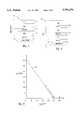
- FIG. 1is a cross-sectional view depicting a spin valve sensor made in accordance with this invention
- FIG. 2is a cross-sectional view depicting a GMR sensor made in accordance with this invention.
- FIG. 3is a graph plotting a relationship between a square root of the absolute value of an electronegativity difference (i.e.,
- FIG. 4illustrates three curves plotting the relationship between
- FIG. 5illustrates three curves plotting the relationship between
- FIG. 6illustrates a curve plotting the relationship between
- FIG. 7is a chart that illustrates various exemplary combinations and compositions of FM layers and spacers for use in spin valve and GMR sensors;
- FIG. 8illustrates two curves plotting the electrical resistivity in microohm-cm versus the atomic composition for a Cu--Au alloy system
- FIG. 9illustrates two graphs plotting the electrical resistivity in microohm-cm versus the atomic composition for a CuPt alloy system
- FIG. 10illustrates a use of random crystal orientation in a spin valve sensor made according to the present invention
- FIG. 11illustrates a use of preferred crystal orientation in a spin valve sensor made according to the present invention
- FIG. 12is a cross-sectional view of a spin valve sensor with compound interfaces made according to the present invention.
- FIG. 13is a cross-sectional view of a giant magnetoresistive sensor with compound interfaces made according to the present invention.
- FIG. 1is a partial cross-section representing a spin valve magnetoresistive (MR) sensor 10 made according to the present invention.
- the spin valve sensor 10is formed of two FM layers (i.e., FM1 and FM2), that are separated by a conductive spacer or layer 12.
- the sensor 10is formed on a nonmagnetic substrate on which a buffer layer, about 25-100 Angstroms (A°) thick, is deposited.
- the buffer layeris made from Ta, Cr, Fe, Pt, Pd, Ir or Au.
- the FM layers FM1 and FM2may have the same or different composition.
- the magnetization of one of the FM layersmay be pinned by placing it in atomic contact with an antiferromagnetic (AFM) layer 14, such as an FeMn layer.
- AFMantiferromagnetic
- the application of an external magnetic fieldcauses a variation in the magnetization orientation of the FM layer FM1, which causes a change in the spin-dependent scattering of conduction electrons and thus in the electrical resistance of the spin valve sensor 10.
- the resistance of the spin valve sensor 10changes as the relative alignment of the magnetization of the FM1 layer changes.
- the FM2 layerremains constrained and its magnetization direction remains the same.
- the present inventionincludes an empirical relationship between ⁇ R/R and the electronegativity difference between adjacent FM layers and conductive spacer layers in spin valve and GMR sensors. This relationship applies to both spin valve and GMR sensors, and shows that ⁇ R/R response is a function of the electronegativity mismatch between adjacent FM layers and conductive spacers. It is believed that the mismatch in electronegativities results in a potential barrier at the interface that is related to the absolute value of the difference in the electronegativities of the FM layers and the conductive spacers, i.e.,
- the ⁇ R/R amplitude of the spin valve and GMR sensorswill decrease to a point where ⁇ R/R will approach an intercept value of zero. As shown later, this intercept value uniformly occurs at a value of
- the spin valve sensor 10(FIG. 1) is formed by selecting the desired spacer material. Subsequently, the FM layers FM1 and FM2 are selected such that their average electronegativities match or substantially approximate the average electronegativity of the selected spacer 12.
- the FM and spacer layerspreferably should have the same or similar crystal structure, e.g., a face-centered cubic (“FCC”) FM layer adjacent to an FCC conductive spacer layer or a body-centered cubic (“BCC”) FM layer adjacent to a BCC spacer layer.
- FCCface-centered cubic
- BCCbody-centered cubic
- These combinationsare referred to herin as “FCC Systems” and “BCC Systems", respectively.
- reported in an FCC Systemis in the range of approximately 0.12 eV.
- a GMR devicecomprising 70Co:30Fe FM layers and Ag spacers exhibited a ⁇ R/R of approximately 100 with a
- reported in a BCC Systemis in the range of approximately 0.07 eV.
- the GMR device described previouslyi.e., Fe/Cr
- the GMR device described previouslyi.e., Fe/Cr
- magnetoresistive sensors according to the inventioncan achieve lower
- FIG. 2illustrates the use of the present inventive concept in a GMR sensor 20.
- the GMR sensor 20is a sandwich structure formed of a plurality of layers, such as FM materials, that are separated by a plurality of conductive spacers 22.
- the FM/spacer structurecan have a multiplicity of repeat units of FM/spacer.
- the electronegativities of each of the successive layers FMare substantially matched or their difference in ⁇ is minimized with respect to the electronegativity of the contiguous spacers 22.
- FIG. 3illustrates that the linear relationship of the invention is generally maintained irrespective of the composition of the FM and spacer materials. Further, FIG. 4 illustrates that the linear relationship is maintained over a wide range of measurement temperatures.
- FIG. 5illustrates that linear relationship holds for a variety of FM alloy compositions for a fixed spacer element. Further, FIG. 6 illustrates that the linear relationship holds for both FCC Systems and BCC Systems.
- the percent ionic content of an interface A/B between an FM layer A and a conductive spacer Bcan be estimated by the electronegativity difference between the FM A and the spacer B as shown in the following equation (Pauling, "The Nature of the Chemical Bond", 98 (1060, 3d)):
- the excess ionic energy at the FM/spacer interfacecan be estimated to be 1.96 Kcal or 0.085 eV (Pauling, Table 3-6 at page 90).
- This energy termrelates to the electron transmission at the interface, which influences ⁇ R/R.
- 1/2equal to 0.5 electron volts, the probability of electron transmission through a potential barrier at the interface is approximately 0 percent.
- the bulk resistivities of the materials used in the FM layers and conductive spacersbe relatively low to ensure a high ⁇ R/R sensor output.
- the bulk resistivities of the FM layer materialbe less than 100 microohm ( ⁇ ) cm, and the spacer material be less than 30 ⁇ -cm.
- ⁇ (FM)represents the electronegativity of the FM layers
- ⁇ (spacer)represents the electronegativity of the spacer 12
- ⁇ (spacer) and ⁇ (FM)are the work functions of the spacer 12 and FM layers, respectively, as stated in Lange, "Handbook of Chemistry", 3-9 (1973, 11d). Both ⁇ and ⁇ values are expressed in electron volts (eV.).
- Each chemical elementhas a work function ⁇ from which the ⁇ of that element is computed by equations (1b) or (1c).
- the ⁇ of such mixtureshas been found to be an additive property of the constituents of the alloy.
- the ⁇ of the mixtureis the sum of the products of the atomic fraction of any element in the mixture times the electronegativity of that element summed over all elements constituting the mixture, as illustrated in the following equation:
- Equation (2)refers to the atomic fractions of elements a, b and c, respectively forming the alloy; and ⁇ a , ⁇ b and ⁇ c refer to the electronegativities of elements a, b and c, constituting the alloy. While only a ternary alloy has been considered for illustration purpose, it should be understood that the form of equation (2) is applicable to alloys with any number of elements. In addition, equation (2) applies both to ferromagnets and conductors.
- Prior art methods for fabricating spin valve and GMR sensorsincluded combining spacers made of an electrically conductive elements such as Au, Ag or Cu, with layers of FM materials such as FeCo, NiFe, or elements such as Fe, Co and Ni, without regard to the electronegativity matching between the successive FM layers and conductive spacers. These prior art methods are mainly based on trial and error studies.
- Tables I and IIprovide listings of some exemplary conductors and ferromagnets, (i.e., FCC Systems and BCC Systems), respectively, that can be used to fabricate various devices, including but not limited to magnetoresistive sensors according to the invention.
- the randomly oriented valuewas added to the previously described work function values and used to compute a second average work function value, which was then used to compute the ⁇ values below.
- equation (2)was used to compute the ⁇ values below.
- the electronegativities of the conductors and the ferromagnetsrepresent the atomic fraction weighted electronegativities, as illustrated by the following example for Cu 3 Pt:
- This exampleillustrates that the atomic fraction of the electronegativities of the elements of any alloy conductor or ferromagnet formed of any number of elements, i.e., ternary, quaternary, etc., can be used to calculate the electronegativity of the alloy.
- Table Iit is possible to closely match the electronegativities of the conductors and the ferromagnets. For example, having selected Cu 3 Pt as the conductor of choice, it would be desirable to select a FM material having a close electronegativity. Table I indicates that one of the closest materials whose electronegativity matches that of Cu 3 Pt is Ni 3 Mn, since the average electronegativity of Ni 3 Mn is 2.01 and ⁇ of the combination is approximately
- Another aspect of the inventionconcerns the use of materials exhibiting superlattice structures for FM layers and spacers in GMR and spin valve sensors.
- the prior artdoes not teach or disclose the use of such superlattice structures in MR sensors.
- Significant advantages in MR device performancecan be achieved with such superlattice structures, even without the matching of ⁇ values.
- Ni 3 Mna ferromagnetic superlattice intermetallic compound having an electronegativity of 2.01 may be matched with Cu 3 Pt, as described in Example 1.
- the matching of two superlattice structuresis desirable in that these ordered structures will improve the thermal stability of sensors containing them. It is believed that this is due to the additional external thermal energy that would be required to disorder one or both superlattice structures before the elements contained in the superlattice would be free to diffuse at the interface. This additional energy ranges between 0.1 eV to 0.3 eV above the activation energy for diffusion across the interface between the conductor spacer and the FM layer and accordingly leads to greater thermal stability of the device. Greater corrosion resistance would also be achieved for such devices.
- a subsequent inquirymay then be made as to whether there exists another ferromagnet with other desirable characteristics, such as minimal magnetostriction ( ⁇ s ) higher corrosion resistance, and/or lower resistivity than Ni 3 Mn.
- Ni 3 Fealso a superlattice alloy, with an electronegativity of 2.07, may in certain applications present a more desirable match than Ni 3 Mn, due to low coercivity (H c ), low ⁇ s and superior corrosion resistance and may be matched with a CuAu superlattice having an ⁇ of 2.07.
- This exampleidentifies conductive spacer alloys useful for the matching or minimizing the ⁇ values between the spacer alloys and appropriate ferromagnetic elements or alloys thereof.
- binary, ternary or higher order alloys of elementssuch as Cu, Ag, Au, Pt, Pd, Ir, Rh and Ru may be used to match appropriate FMs and provide ⁇ values ranging from approximately 1.89 to 2.33.
- Such alloysmay be used to fabricate various devices, including but not limited to spin valve and GMR sensors, based on the electronegativity matching or minimizing of the differences in electronegativities of the present invention.
- Other superlattice alloys similar to CuPt and CuAu that exhibit ordering phenomena, such as Ag 3 Pt and AgPt,may also be used for implementing this invention.
- a subsequent inquirymay then be made as to whether the crystallographic structures of the adjacent conductive spacer and the FM layer are matched. It is desirable to match the crystallographic structures of adjacent layers.
- additional intermetallic compounds having a FCC crystallographic structure for use as conductive spacer materialsare listed:
- a number of the above elementssuch as W, Ta and Mo occur in high resistivity structures when deposited by evaporation or sputtering.
- deposition parameterssuch as rates, substrate temperatures, and partial inert gas pressures, e.g., Ar
- a low resistivity structurecan be obtained, which is preferred for spacers in spin valve and GMR structures.
- FIG. 3illustrates the linear relationship between the magnetoresistive response as characterized by ⁇ R/R of the spin valve sensor 10 (FIG. 1), relative to a square root of the absolute value of the electronegativity difference, (i.e.,
- This linear relationshipis represented by a curve S1. It is maintained for various spin valve layer compositions, representing a variety of spacer materials and FM materials and illustrates that the variable ⁇ controls ⁇ R/R. This relation may be expressed generally by the following equation (3):
- Sample preparation variablesmay affect the slope B of this equation (3). It is generally recognized in the literature that a certain degree of roughness at the interface between the FM layers and the conductive spacers produces a maximum result ( ⁇ R/R) for a given interface, for instance, Dieny, "Giant Magnetoresistance in Spin-Valve Multilayers", Journal of Magnetism and Magnetic Materials, 136 (1994) pp. 335-359. As the roughness increases or decreases from its optimal value ⁇ R/R will decrease from its optimal value. This will change the slope B, but will not modify the general principles of the invention. Roughness variations will also not modify the intercept where ⁇ R/R equals 0, which remains at
- equation (3)may be expressed as follows:
- the general equation (3)may be expressed by the following experimentally derived equation (5) for spin valves formed by a variety of interfaces:
- Point D on curve S1 in FIG. 3represents the following FM layer/spacer compositions: Co/Cu/Co, where the first element Co is the unpinned FM layer FM1, the second element Cu is the conductive spacer 12 (FIG. 1), and the third element Co is the pinned FM layer FM2.
- the composition of this exampleyields a ⁇ R/R of approximately 9.5 percent.
- Point E on curve S1 in FIG. 3represents Co/Cu/80Ni:20Fe, where the first element Co is the unpinned FM layer FM1 (FIG. 1), the second element Cu is the conductive spacer 12, and the third element 80Ni:20Fe is the pinned FM layer FM2.
- the composition of this exampleyields a ⁇ R/R of approximately 6.5 percent.
- Point F on curve S1 in FIG. 3represents 80Ni:20Fe/Cu/80Ni:20Fe, where the first element 80Ni:20Fe is the unpinned FM layer FM1 (FIG. 1), the second element Cu is the conductive spacer 12, and the third element 80Ni:20Fe is the pinned FM layer FM2.
- the composition of this exampleyields a ⁇ R/R of approximately 5 percent.
- Point G on curve S1 in FIG. 3represents Co/Au/80Ni:20Fe, where the first element Co is the unpinned FM layer FM1 (FIG. 1), the second element Au is the conductive spacer 12, and the third element 80Ni:20Fe is the pinned FM layer FM2.
- the composition of this exampleyields a ⁇ R/R of approximately 4.5 percent.
- Point H on curve S1 in FIG. 3represents Ni/Cu/Ni, where the first element Ni is the unpinned FM layer FM1 (FIG. 1), the second element Cu is the conductive spacer 12, and the third element Ni is the pinned FM layer FM2.
- the composition of this exampleyields a ⁇ R/R of approximately 2.5 percent.
- Point I on curve S1 in FIG. 3represents 80Ni:20Fe/Pt/80Ni:20Fe, where the first alloy 80Ni:20Fe is the unpinned FM layer FM1 (FIG. 1), the second element Pt is the conductive spacer 12, and the third alloy 80Ni:20Fe is the pinned FM layer FM2.
- the composition of this exampleyields a ⁇ R/R of approximately 0.3 percent.
- Point J on curve S1 in FIG. 3represents 80Ni:20Fe/Pd/80Ni:20Fe, where the first alloy 80Ni:20Fe is the unpinned FM layer FM1 (FIG. 1), the second element Pd is the conductive spacer 12, and the third alloy 80Ni:20Fe is the pinned FM layer FM2.
- the composition of this exampleyields a ⁇ R/R of approximately 0.2 percent.
- Point K on curve S1 in FIG. 3represents 80Ni:20Fe/Al/80Ni:20Fe, where the first alloy 80Ni:20Fe is the unpinned FM layer FM1 (FIG. 1), the second element Al is the conductive spacer 12, and the third alloy 80Ni:20Fe is the pinned FM layer FM2.
- 1/2 between Al and its adjacent first alloy layer FM1is approximately 0.6/eV, which is greater than the intercept point value of 0.5 eV. In this and other similar examples where
- FIG. 4illustrates the temperature insensitivity of the linear relationships between the ⁇ R/R of the spin valve sensor 10 (FIG. 1) relative to the square root of the absolute value of the electronegativity difference
- the responseis shown at three different measurement temperatures, that is, 300° K., 200° K. and 100° K.
- unpinned FM layer FM1Co (point a), 80Ni:20Fe (point b), and Ni (point c),
- conductive spacerCu with an approximate thickness of 22A°.
- the ⁇ values used for the FM layersare the average of pinned and free layers, ( ⁇ free + ⁇ pinned )/2.
- This exampleis represented by the curve V2 and graphically plots the linear relationship at a temperature of 200° K. Points d, e and f reflect data observed for similar compositions as in Example 15 above.
- This exampleis represented by the curve V3 and graphically plots the linear relationship at a temperature of 300° K. Points g, h and i reflect data observed for similar compositions as in Examples 15 and 16 above.
- the conductive spacer separating the FMsis generally between 18A° and 30A° thick, while the FMs generally range between 30A° and 120A° with an optimum thickness typically near 60A° each.
- FIG. 5illustrates that the linear relationship of equation (3) for the GMR sensor 20 (FIG. 2) is exhibited for distinct MR peaks at particular spacer thicknesses. ⁇ R/R was measured at room temperature, for various Co Ni alloys. The resulting relationship s are represented by three exemplary curves G1, G2, G3, and are for various GMR FM layer compositions.
- the curves G1, G2, G3may be expressed generally by the following equations (6), (7) and (8), that continue to verify the relationships of equations (3) and (4).
- Curve G1 in FIG. 5may be expressed by the following equation (6), and represents the GMR first peak at a Cu thickness of approximately 10A°:
- Curve G2 in FIG. 5may be expressed by the following equation (7), and relates to the second GMR peak at a Cu thickness of approximately 22A°:
- Curve G3 in FIG. 5may be expressed by the following equation (8), and represents the third GMR peak at a Cu thickness of approximately 32A° to 36A°:
- peaks 1 through 4While only three GMR peaks are shown in FIG. 5, well defined peaks at a fourth position (i.e., peaks 1 through 4) have been observed in GMR devices. These peaks generally occur at spacer thicknesses of approximately 10°, 20A°, 30A° and 40A°. It is known that both the peak ⁇ R/R and the switching field required to attain the maximum value of ⁇ R/R (at any peak) decline with increasing peak number (and increasing spacer thickness). However, the switching field at each increasing peak declines more rapidly than does ⁇ R/R at each peak. Thus, the sensitivity of the transducer as measured by ⁇ R/R/Oersted of switching field improves dramatically with increasing peak number.
- the present inventionis particularly useful in extending GMR performance to higher peak values at lower switching fields due to the minimizing of ⁇ between FM and spacer layers.
- the present inventionmaximizes the device sensitivity at any peak but is most useful at large peak numbers that are inherently more sensitive, i.e., achieving a larger ( ⁇ R/R/Oersted) than has been reported.
- the FM layersmay range in thickness from approximately 4A° to 25A°.
- the following exemplary embodimentsdemonstrate that by a proper selection of the composition of the materials forming the sensor 20 (FIG. 2), and by matching or substantially minimizing the absolute electronegativity difference (or mismatch) of the sensor layers (FM layers and conductive spacers), it is possible to obtain significantly higher output signals ( ⁇ R/R) than those previously attained.
- the foregoing linear relationshipswere mostly obtained using data at room temperature. Further analyses confirm that these relationships are also valid for data obtained or derived at other temperatures, including the sensor normal operating temperatures of approximately 45° C. and cryogenic temperatures as well. However, the slopes of the curve G1, G2 and G3, i.e., the value B, will vary at different temperatures.
- An important aspect of the present inventionmay be derived from equations (6), (7) and (8), namely that all the curves G1, G2 and G3 converge at a single intercept point (I), at which ⁇ R/R equals 0, and
- an optimal interfacial surface roughnessshould be selected to maximize the slopes of any curve G1, G2 or G3 and thereby achieving a maximum ⁇ R/R for any interface ⁇ of the FM and spacer layers.
- FIG. 5shows FIG. 5 shows the value of ⁇ R/R for a GMR structure at three peaks as a function of the following NiCo alloy compositions for the FM layer.
- G1On the first GMR peak curve G1 in FIG. 5, the following points represent the stated compositions:
- points R1 and S1correspond to the respective compositions of points J1, H1, and M1 along the first peak curve G1.
- R1is 50Ni:50Co
- S1is 70Ni:30Co
- T1is 80Ni:20Co
- U1is Ni.
- V1is 30Ni:70Co
- W1is 50Ni:50Co
- X1is 70Ni:30Co
- Y1is Ni.
- FIG. 6illustrates that the linear relationship of equation (3) for the GMR sensor 20 (FIG. 2) at a temperature of 5° K. is maintained when a BCC Systems is observed.
- the linear relationshipis represented by an exemplary curves R1 (FIG. 6).
- the exemplary compositionsare expressed as X-Y, where element X represents the material for the FM layers, and element Y represents the material for the conductive spacers 22.
- Points i1 and j1both have FM and conductive spacer materials with FCC crystal structures (i.e., an FCC System).
- the FM and spacer materials at point g1have BCC structures (i.e., a BCC System), and the latter point is also predicted by the linear relationship of the invention.
- curve R1 in FIG. 6may be expressed by the following equation (9), and relates to the GMR first peak:
- Point p on FIG. 6represents the GMR structure Fe Cu.
- This structurepresents an almost perfect electronegativity match (i.e., (
- a BCC element or alloymay be forced by epitaxial effects of an underlying FCC metal or alloy to form an FCC structure for a few monolayers (i.e., 0.5 to 7 monolayers (ML)).
- the reciprocal situationi.e., an FCC material on a BCC material
- FCC Systemssome face centered tetragonal structures, representing nearly FCC systems, may be used to advantage as well.
- FIG. 7is a chart that illustrates various exemplary combinations and compositions for the FM layers and spacers, some of which are explained by the following examples.
- the FM layersmay be selected from a group comprised of Fe, Co, Ni, and their alloys and their substitutional alloys.
- the conductive spacer layersmay be selected from a group comprised of Au, Cu, Ag, Rh, Pt, Pd and substitutional alloys thereof, and other suitable elements or intermetallic compounds possessing sufficiently low resistivities.
- the Heusler alloys shown in FIG. 7will be discussed later.
- FIG. 8shows two curves, SL1 and SL2, plotting the electrical resistivity in microohm-cm versus the atomic composition for the Cu Au alloy system.
- Curve SL1illustrates the relationship for alloys that have been quenched and cold worked (i.e., in a disordered state).
- Curve SL2illustrates the relationship for alloys that are annealed at 200° C. for the purpose of achieving an ordered superlattice structure.
- FIG. 8further shows that the electrical resistivities of the ordered alloy relative to the same composition of the disordered alloy may be reduced significantly by annealing the alloys having predetermined atomic compositions.
- compositionsat which the electrical resistivities of the alloys exhibit a minimum, are a result of an ordered superlattice and will be referred to herein as Critical Points (CP). Additional description of superlattice structures may be found in C. Barrett, "Structure of Metals, Crystallographic Methods, Principles, and Data", 269-296 (1952 2d) which is incorporated herein by reference.
- FIG. 9shows two curves SL3, SL4, plotting the electrical resistivity versus atomic composition for the Cu Pt alloy system.
- Curve SL3illustrates the relationship for alloys that are quenched and cold worked (disordered state).
- Curve SL4illustrates the relationship for alloys that are annealed at 300° C. for achieving an ordered superlattice structure.
- FIG. 9further shows that the specific electrical resistivities of the ordered superlattice may be reduced significantly by annealing the alloys at two critical points CP3 (25 atomic percent Pt), and CP4 (50 atomic percent Pt).
- points CP1 and CP2(FIG. 8), and points CP3 and CP4 (FIG. 9) reflect the most useful compositions
- other compositions defined by the hatched areas A1 (FIG. 8) and B1, B2 (FIG. 9) between the envelopes of the disordered alloys (SL1, SL3) and the envelopes of the ordered alloys (SL2, SL4)may also be useful in providing a broader electronegativity selection range, while at the same time producing a partially ordered superlattice that will have some benefit in extending the thermal stability of spin valve and GMR sensors using the ordered alloys.
- the two alloy series in examples 22 and 23may be annealed at between 100° C. to 300° C. in thin film form for approximately 0.5 hour to 4 hours to form the superlattice or partially ordered superlattice at appropriate composition.
- the inventionuses the superlattices processed at or near critical points CP or within any of the shaded regions in the Cu Au binary system or the Cu Pt binary system or other binary systems.
- the shaded regionsdefine the composition range within which some degree of superlattice order will occur and which may be used advantageously.
- the most advantageous compositions from a resistivity point of vieware a 25 and 50 atomic percent Cu for both the Cu Au and Cu Pt systems.
- a superlattice spacer 22(FIG. 2) will provide a large mean free path for electrons in the spacer while simultaneously minimizing the electronegativity difference
- the Cu Pt superlattice alloy(FIG. 9) exhibits a resistivity of about 3.5 ⁇ -cm, which is similar to the resistivity of gold, and an average electronegativity of approximately 2.07 eV.
- 80Ni:20Feis used as an FM layer.
- the electronegativity of 80Ni:20Feis about 2.084 eV and the electronegativity of the CuPt superlattice alloy CP4 is approximately 2.07 eV, resulting in an absolute electronegativity difference
- This excellent matchwill significantly minimize the detrimental interfacial scattering component in the spin valve sensor 10 (FIG. 1) and the GMR sensor 20 (FIG. 2), and results in maximizing sensor signal output ⁇ R/R.
- This examplealso exhibits improved corrosion resistance and thermal stability. In addition, adverse electromigration effects in the sensor are minimized.
- the Cu Au superlattice alloy CP2 of Example 22(FIG. 8) is used as a spacer, while Co is used as an FM layer. Since the electronegativity of Co is about 2.05 eV and the electronegativity of the Cu Au superlattice alloy CP2 is approximately 2.07 eV, thus resulting in an absolute electronegativity difference ⁇ of 0.02, which provides an excellent electronegativity match.
- a Cu Au superlattice CP2(FIG. 8) is used as a spacer, while an Ni 3 Fe superlattice composition forms the FM layers.
- the average electronegativity of the Cu Au superlattice CP2is about 2.07, which has an absolute electronegativity difference of about 0.01 with the Ni 3 Fe superlattice.
- the dual superlattice structureincreases the thermal stability as well as the chemical stability of the sensors 10 and 20 (FIGS. 1 and 2). Since the superlattice alloys are greatly more corrosion resistant than copper and the ferromagnet alloys, the sensors 10 and 20 using the superlattices formed at or near CPs result in a structure of superior electromigration characteristics as well.
- one method for processing the superlattice alloysis to anneal them between 100° C. to 300° C. for 10 to 200 minutes.
- An alternative methodis to deposit the superlattice alloys by sputtering or evaporation, at a relatively low rate, on a sufficiently heated substrate. This slow deposition process could form the superlattice structure without the need for further thermal annealing.
- the materials that may be used for FM layers to achieve the preceding objective of minimizing ⁇are from the group of alloys constituting (1) Fe, Ni, Co, or any combination of these elements, and (2) any of the following elements or combinations thereof: Au, Cu, Cr, Mn, Ti, V, Pt, Pd, Ru, Ir, Sn, Ta, Nb, Rh, N, C, Zr, Hf, Y, La, and rare earth elements, having either FCC or BCC structures or in amorphous forms containing a combination of the above elements.
- Appendix AA more extensive list of ⁇ values that may be used to implement the invention is provided in Appendix A, which is incorporated by reference. The values of ⁇ in Appendix A were calculated using the data and methods described previously in reference to Tables I and II.
- yis an atomic fraction of Pd with a value between 0.12 to 0.30. These alloys display near zero magnetostriction and low coercivity.
- each alloyhas near zero magnetostriction and have ⁇ values of 2.13.
- Each alloycan be matched with the superlattice conductive spacer of CuPt whose ⁇ is approximately 2.12:
- FIG. 10illustrates the use of randomly oriented crystals in the spin valve sensor 10 of FIG. 1.
- the crystalline orientation of the substrateis random, and therefore the three crystallographic orientations (i.e., ⁇ 100>, ⁇ 110>, ⁇ 111>), have approximately the same frequency of surface occupancy on the substrate.
- the FM layer that is formed on top of the substratewill develop the same random orientation as the substrate by epitaxy. It is an object of the present invention to match the average electronegativity of each layer to the average electronegativity of the adjacent layers.
- the following example 28illustrates the effect of the mismatch of the electronegativity
- FM and spacer layers having a single crystallographic orientationthat will maximize ⁇ R/R, e.g. Ni FM layers and Cu spacer layers each having ⁇ 111>crystal orientations, and achieve significant improvement in spin value sensor performance.
- ⁇ R/Re.g. Ni FM layers and Cu spacer layers each having ⁇ 111>crystal orientations
- FIG. 11illustrates the use of polycrystalline FM layers and spacers having a preferred orientation in the spin valve sensor 10 of FIG. 1.
- the surface crystalline orientation of the substratehas been selected to be ⁇ 111>.
- the subsequent crystal FM layer and spacers that are formedwill develop the same ⁇ 111> surface orientation. It is an object of the present invention to match the electronegativities of the selected crystalline orientation, which in this example is ⁇ 111>, of the juxtaposed layers, rather than to match the average electronegativities of these layers.
- the spin valve sensor 10(FIG. 1) is formed by selecting a desired spacer material and a preferred one of its three main crystalline orientations, for example ⁇ 111>. Subsequently, the FM layers are selected such that the ⁇ of their corresponding faces with a ⁇ 111> crystalline orientation matches or substantially approximates the ⁇ of the selected spacer crystalline face (i.e., ⁇ 111>). Similarly, the ⁇ 110> and ⁇ 100> surface faces can be matched as well by selecting the proper alloys.
- a preferred crystal orientationi.e., ⁇ 111>, ⁇ 100> or ⁇ 110>
- a substratesuch as magnesium oxide with a surface orientation of either ⁇ 111>, ⁇ 100> or ⁇ 110>.
- the surface roughness of each selected orientationis optimized by optimizing the deposition conditions for each orientation. In this way, a maximum ⁇ R/R can be achieved for each principal orientation (i.e., ⁇ 111>, ⁇ 100> or ⁇ 110>).
- FIGS. 12 and 13illustrate a spin valve sensor 10A and a GMR sensor 20A respectively comprised of compound FM layers.
- the spin valve sensor 10Aincludes two or more compound FM layers (FM1/FM2) and (FM3/FM4), each of which are composed of different ferromagnetic materials.
- the GMR sensor 20Aincludes a plurality of electrically conductive spacers, such as Spacer 1 and Spacer 2, that are interposed between and compound FM layers, such as (FM1/FM2), (FM3/FM4), (FM4/FM5) and (FM6/FM7).
- the FM materials for these compound layersshould be selected so that the values of ⁇ s and H c for each material (e.g. FM1 and FM2) will combine to produce low values of ⁇ s and H c , for the layers (e.g. FM1/FM2). Further, the interfaces between the FM layers and spacers (e.g. FM2/Spacer and FM3/Spacer) follow the electronegativity matching and other selection criteria described herein.
- FM1 and FM4may be identical compositions, or may be different compositions, and the same applies to FM2 and FM3. It may be advantageous, however, that FM2 and FM3 have the same composition and that FM1 and FM4 have the same composition in order to simplify processing because fewer sputtering targets would be needed.
- the basis for having two or more different compositions for FM1 and FM2is that the magnetostriction thickness product of FM1 and FM2 may be selected so that ⁇ FM1 t FM1 is approximately equal to - ⁇ FM2 t FM2 , where t is FM layer thickness, resulting in minimizing an average ⁇ s for both layers, which average ⁇ s desirably approaches zero for the compound FM interfaces. It is not necessary to absolutely match the magnetostriction thicknesses products in order to minimize magnetostriction. For example, if the ratio of magnetostriction thickness products is even in the range of 0.3 to 3, the overall ⁇ s of the compound FM layer FM1/FM2 will be reduced. Even an unbalanced thickness product of each layer will lower ⁇ s , which minimizes ⁇ s of a compound FM layer structure.
- the use of compound FM layeralso enables the minimization of the overall H c of the layers because the H c of the layer is generally the average of the H c values for each FM material forming the layer (i.e., FM1 and FM2).
- the H c of the layeris generally the average of the H c values for each FM material forming the layer (i.e., FM1 and FM2).
- an FM2 selected for a good ⁇ match with the spacermay have a high H c .
- This adverse effectcan be mitigated by selecting an material for FM1 that has a very low H c , without regard to matching its ⁇ with that of the spacer.
- a low H c for the compound FM layerssuch as less than 10 oersteds, may be obtained.
- the ⁇ of the FM layer adjacent to the spacers(e.g., FM2 or FM3) be minimized relative to the ⁇ of the adjacent spacer. Similar conditions apply to the GMR structure of FIG. 13 as well.
- the compound FM structure in spin valve structures and GMR structuresin combination with the preceding teaching requiring the minimization of ⁇ between FM and spacer, allows for maximizing ⁇ R/R while simultaneously maximizing corrosion resistance and minimizing the ⁇ s and H c of compound ferromagnet structures of spin valve structures or GMR structures or GMR structures.
- Heusler alloysrepresent another class of ferromagnetic materials possessing a superlattice structure that may be partially or fully ordered. Full ordering is possible at or very near to the general stoichiometric composition M 2 MnM 1 and may contain ferromagnetic elements Co and Ni as well as the nonferromagnetic elements Cu, Ir, Pd, Pt and Au for M 2 .
- M 1may be Al, Ga, Ge, As, In, Si, Sn or Bi.
- the Heusler alloys containing only Pt, Au, Pd or Ir for M 2i.e., M 2 having a full complement of such element, e.g., Au 2 ), exhibit Curie temperatures below room temperatures (i.e., below 300° K.).
- Such alloysmay, if they are not ferromagnetic and their bulk resistivity is less than approximately 30 ⁇ -cm, be used as spacers for other ferromagnetic Heusler alloys. It is also possible to combine the following elements in M 2 : Cu, Co, Ni, Pd, Pt, Au and Ir, for the purpose of fine control of the electronegativity of the Heusler alloy to minimize ⁇ of the Heusler alloy and its spacer element or alloy or compound.
- the FM Heusler alloysmay be used in conjunction with spacer materials such as Cu, CuAu alloys (with Au of 5 to 15 atomic percent) and intermetallic spacers Al 2 Au (with ⁇ equal to 1.88) and PtAl 2 (with ⁇ equal to 1.92).
- spacer materialssuch as Cu, CuAu alloys (with Au of 5 to 15 atomic percent) and intermetallic spacers Al 2 Au (with ⁇ equal to 1.88) and PtAl 2 (with ⁇ equal to 1.92).
- AgAu alloysmay be used as well with Au less than 25 atomic percent.
- a method and meansare provided for selecting the materials for spin valve and GMR sensors which simultaneously may have higher magnetoresistance output, improved corrosion resistance, improved coercivity, improved thermal stability of the interfaces and improved electromigration properties.
- a method and meansare provided for selecting the materials for spin valve and GMR sensors which simultaneously may have higher magnetoresistance output, improved corrosion resistance, improved coercivity, improved thermal stability of the interfaces and improved electromigration properties.
Landscapes
- Engineering & Computer Science (AREA)
- Chemical & Material Sciences (AREA)
- Nanotechnology (AREA)
- Physics & Mathematics (AREA)
- Crystallography & Structural Chemistry (AREA)
- Manufacturing & Machinery (AREA)
- Power Engineering (AREA)
- Condensed Matter Physics & Semiconductors (AREA)
- General Physics & Mathematics (AREA)
- Theoretical Computer Science (AREA)
- Mathematical Physics (AREA)
- Spectroscopy & Molecular Physics (AREA)
- Hall/Mr Elements (AREA)
- Micromachines (AREA)
- Magnetic Heads (AREA)
Abstract
Description
Percent Ionic Content=(1-e.sup.(χA-χB).spsp.2/4)×100
|Δχ|=χ(FM)-χ(spacer), (1a)
χ(spacer)=0.44φ(spacer)-0.15, (1b)
χ(FM)=0.44φ(FM)-0.15, (1c)
χ.sub.(a-b-c) =f.sub.a χ.sub.a +f.sub.b χ.sub.b +f.sub.c χ.sub.c, (2)
TABLE I ______________________________________ FCC SYSTEMS CON- DUCTORS χ (eV.) FERROMAGNETS χ (eV.) ______________________________________ Cu 1.91 80Ni:20Fe 2.084 Ag 1.89 Ni.sub.3 Fe.sup.(4) 2.07 Ag.sub.3 Pt.sup.(5) 2.00 Au 2.22-2.27.sup.(3) Ni.sub.3 Mn.sup.(4) 2.02 Fe.sub.4 N 2.12 Pt 2.34 FePd 2.11 Pd 2.32 Fe.sub.1-y Au.sub.y.sup.(1) 2.0 ≦ χ ≦ 2.13 Cu.sub.3 Pt.sup.(4) 2.02 Co.sub.1-z Au.sub.z.sup.(2) 2.07 ≦ χ ≦ 2.14 CuPt.sup.(4) 2.13 Fe.sub.0.485 Ni.sub.0.418 Mn.sub.0.097 1.99 CuPt.sub.3.sup.(4)(5) 2.23 80Ni:20Fe 2.084 Cu.sub.3 Pt.sub.5.sup.(4)(5) 2.18 81Ni:19Fe 2.086 Cu.sub.3 Au.sup.(4) 1.99-2.00.sup.(3) 90Co:10Fe 2.04 Cu.sub.3 Pd.sup.(4)(5) 2.01 80Ni:20Fe 2.084 CuPd.sup.(4) 2.06 Rh 2.04 CuAu.sup.(4)(5) 2.07-2.09.sup.(3) ______________________________________ .sup.(1) Where y is an atomic fraction with a value between 0.30 and 0.70 .sup.(2) Where z is an atomic fraction with a value between 0.10 and 0.50 .sup.(3) the higher stated values for χ reflect the use of a larger work function for the <111> face of Au than that stated in Michaelson, which adjustment appears necessary when work function data for <111> face of other FCC elements is compared to <110> work function data; and .sup.(4)(5) a pseudocubic structure, the stated composition is a superlattice structure.
TABLE II ______________________________________ BCC SYSTEMS CONDUCTORS χ FERROMAGNETS χ ______________________________________ Cr 1.83 Fe.sub.1-u Cr.sub.u.sup.(1) 1.85 ≦ χ ≦ 1.88 Cr 1.83 Fe.sub.1-w V.sub.w.sup.(2) 1.85 ≦ χ ≦ 1.87 Cr 1.83 Ternary FeCrV 1.84 ≦ χ ≦ 1.87 alloys Cr 1.83 Fe.sub.3 Al.sup.(3) 1.86 AlFe.sub.2 1.84 ______________________________________ .sup.(1) Where u is an atomic fraction with a value between 0.40 and 0.70 .sup.(2) where w is an atomic fraction with a vaule between 0.25 and 0.35 and .sup.(3) the stated composition is a superlattice structure.
χ(Cu.sub.3 Pt)=0.75χ(Cu)+0.25χ(Pt)=2.02,
______________________________________ χ ______________________________________ AgPt.sub.3 2.23 CrIr.sub.3 2.20 Cr.sub.2 Pt 2.00 ______________________________________
______________________________________ χ χ χ ______________________________________ Cr 1.83 V 1.74 Mo 1.83 W 1.80 Nb 1.74 Ta 1.67 ______________________________________
ΔR/R≅A-B|Δχ|.sup.1/2,(3)
ΔR/R≈A-2A|Δχ|.sup.1/2(4)
ΔR/R=32.3-64.6|Δχ|.sup.1/2.(5)
ΔR/R≅245-490|Δχ|.sup.1/2.(6)
ΔR/R≅110-220|Δχ|.sup.1/2.(7)
ΔR/R≅45-90|Δχ|.sup.1/2.(8)
______________________________________ Point X Y ______________________________________ g1 Fe Cr i1 Co Cu j1 Co Ag ______________________________________
ΔR/R≅330-660|Δχ|.sup.1/2(9)
(48Co:29Ni:23Fe).sub.(1-y) Pd.sub.y, and (26Co:44Ni:30Fe).sub.(1-y) Pd.sub.y
33.6Co:20.3Ni:16.1Fe:30Pd,
18.2Co:30.8Ni:21Fe:30Pd.
χ(randomly oriented)=1/3 (χ.sub.111 +χ.sub.100 +χ.sub.110)(10)
______________________________________ Spacer Layer FM Layer Cu (face) χCu (face) Ni (face) χNi (face) |Δχ|.sup.1 /2 (face) ______________________________________ Cu(111) 2.041 Ni(111) 2.204 0.404 Cu(100) 1.87 Ni(100) 2.146 0.525 Cu(110) 1.821 Ni(110) 2.068 0.498 ______________________________________
66R/R=1/3{ 32.30-64.60(0.404)!.sub.111 + 32.30-64.60(0.525)!.sub.100 + 32.30-64.60(0.498)!.sub.110}ΔR/R=1/3 (6.21+0+0.19)%≅2.13%
χ.sub.111 ≃1.027χ.sub.R
χ.sub.100 ≃1.007χ.sub.R
χ.sub.110 ≃0.965χ.sub.R
______________________________________ Heusler Alloy χ Alloy ______________________________________ Cu.sub.2 MnAl 1.80 Ni.sub.2 MnSn 1.93 Co.sub.2 MnGe 1.94 Co.sub.2 MnSi 1.93 Co.sub.2 MnSn 1.89 CuPdMnSn 1.92 NiAuMnSn 1.95 ______________________________________
APPENDIX A ______________________________________ A list of χ values for elements that may be used as ferromagnetic layers and conductive spacers is provided below: Element Polycrystalline χ (eV). Bulk Crystal Structure ______________________________________ Au 2.22 FCC Fe 1.90 BCC Cu 1.91 FCC Ag 1.89 FCC Pt 2.34 FCC Pd 2.32 FCC Ir 2.32 FCC Rh 2.04 FCC Co 2.05 FCC in thin films Ni 2.13 FCC Mn 1.65 Complex Cr 1.83 BCC Ti 1.76 V 1.74 BCC Ru 1.92 CPH close packed hexagonal Sn 1.79 Complex Ta 1.73 BCC Nb 1.75 BCC Zr 1.63 BCC CPH Hf 1.57 CPH Y 1.21 CPH La 1.39 FCC CPH Rare earth ˜1.21 Complex CPH FCC BCC elements C ˜2.52 Various forms N ˜3.01 Gaseous Al ˜1.72 FCC Ge ˜2.00 Si ˜1.96 Bi 1.71 As 1.50 ______________________________________
Claims (25)
ΔR/R≃A-B.linevert split.Δχ.linevert split..sup.1/2,
Priority Applications (5)
| Application Number | Priority Date | Filing Date | Title |
|---|---|---|---|
| US08/702,977US5793279A (en) | 1996-08-26 | 1996-08-26 | Methods and compositions for optimizing interfacial properties of magnetoresistive sensors |
| EP97114191AEP0827220A3 (en) | 1996-08-26 | 1997-08-18 | Methods and compositions for optimizing interfacial properties of transducers used in data storage devices |
| EP97114774AEP0827221A3 (en) | 1996-08-26 | 1997-08-26 | Methods and compositions for optimizing interfacial properties of magnetoresistive sensors |
| JP9246234AJPH10177705A (en) | 1996-08-26 | 1997-08-26 | Magnetoresistance sensor, its production, optimizing method for interface characteristics and optimizing method for magnetoresistance response |
| US09/648,006US6828897B1 (en) | 1996-08-26 | 1998-08-03 | Methods and compositions for optimizing interfacial properties of magnetoresistive sensors |
Applications Claiming Priority (1)
| Application Number | Priority Date | Filing Date | Title |
|---|---|---|---|
| US08/702,977US5793279A (en) | 1996-08-26 | 1996-08-26 | Methods and compositions for optimizing interfacial properties of magnetoresistive sensors |
Related Child Applications (1)
| Application Number | Title | Priority Date | Filing Date |
|---|---|---|---|
| US09/648,006DivisionUS6828897B1 (en) | 1996-08-26 | 1998-08-03 | Methods and compositions for optimizing interfacial properties of magnetoresistive sensors |
Publications (1)
| Publication Number | Publication Date |
|---|---|
| US5793279Atrue US5793279A (en) | 1998-08-11 |
Family
ID=24823431
Family Applications (2)
| Application Number | Title | Priority Date | Filing Date |
|---|---|---|---|
| US08/702,977Expired - LifetimeUS5793279A (en) | 1996-08-26 | 1996-08-26 | Methods and compositions for optimizing interfacial properties of magnetoresistive sensors |
| US09/648,006Expired - Fee RelatedUS6828897B1 (en) | 1996-08-26 | 1998-08-03 | Methods and compositions for optimizing interfacial properties of magnetoresistive sensors |
Family Applications After (1)
| Application Number | Title | Priority Date | Filing Date |
|---|---|---|---|
| US09/648,006Expired - Fee RelatedUS6828897B1 (en) | 1996-08-26 | 1998-08-03 | Methods and compositions for optimizing interfacial properties of magnetoresistive sensors |
Country Status (3)
| Country | Link |
|---|---|
| US (2) | US5793279A (en) |
| EP (2) | EP0827220A3 (en) |
| JP (1) | JPH10177705A (en) |
Cited By (44)
| Publication number | Priority date | Publication date | Assignee | Title |
|---|---|---|---|---|
| US5917400A (en)* | 1995-01-27 | 1999-06-29 | Nec Corporation | Magnetoresistance effects film |
| US5999378A (en)* | 1996-12-27 | 1999-12-07 | Kabushiki Kaisha Toshiba | Magnetoresistance effect head having a giant magnetoresistance effect film |
| WO2000013194A1 (en)* | 1998-08-28 | 2000-03-09 | The Research Foundation Of State University Of New York | Magnetoresistive material with two metallic magnetic phases |
| WO2000063714A1 (en)* | 1999-04-20 | 2000-10-26 | Seagate Technology Llc | GIANT MAGNETORESISTIVE SENSOR WITH A CrMnPt PINNING LAYER AND A NiFeCr SEED LAYER |
| US6154348A (en)* | 1997-06-30 | 2000-11-28 | Nec Corporation | Magnetoresistive head and method of initialization having a non-planar anti-ferromagnetic layer |
| US6166890A (en)* | 1998-07-24 | 2000-12-26 | Seagate Technology Llc | In plane, push-pull parallel force microactuator |
| US6308400B1 (en)* | 1999-08-06 | 2001-10-30 | Headway Technologies, Inc. | Method for achieving anti-parallel exchange coupling with one biased layer having low coercivity |
| US6375761B1 (en) | 1998-08-28 | 2002-04-23 | The Research Foundation Of State University Of New York | Magnetoresistive material with two metallic magnetic phases |
| US6430012B1 (en)* | 1998-03-12 | 2002-08-06 | Tdk Corporation | Magnetoresistance effect film and magnetoresistance effect type head having specified antiferromagnetic promote layer |
| US6456469B1 (en) | 2000-06-05 | 2002-09-24 | International Business Machines Corporation | Buffer layer of a spin valve structure |
| US20020159205A1 (en)* | 2001-04-30 | 2002-10-31 | Witold Kula | Underlayer for high amplitude spin valve sensors |
| US6483675B1 (en)* | 1999-07-23 | 2002-11-19 | Tdk Corporation | Tunnel magnetoresistance effect element |
| US6515573B1 (en)* | 2000-06-19 | 2003-02-04 | Read-Rite Corporation | Method and system for providing edge-junction TMR utilizing a hard magnet as a pinned layer |
| US6563680B2 (en) | 2001-03-08 | 2003-05-13 | International Business Machines Corporation | Spin valve sensor with pinned layer and antiparallel (AP) pinned layer structure pinned by a single pinning layer |
| US20030137785A1 (en)* | 2002-01-24 | 2003-07-24 | Alps Electric Co., Ltd. | Magnetic sensing element containing half-metallic alloy |
| US6600638B2 (en) | 2001-09-17 | 2003-07-29 | International Business Machines Corporation | Corrosion resistive GMR and MTJ sensors |
| US20030161077A1 (en)* | 2000-06-22 | 2003-08-28 | Yasuhiro Kawawake | Magnetoresistance effect device and magnetoresistance effect head comprising the same, and magnetic recording/reproducing apparatus |
| US20030197986A1 (en)* | 2002-04-18 | 2003-10-23 | Ambrose Thomas F. | GMR spin valve structure using heusler alloy |
| US6665155B2 (en) | 2001-03-08 | 2003-12-16 | International Business Machines Corporation | Spin valve sensor with free layer structure having a cobalt niobium (CoNb) or cobalt niobium hafnium (CoNbHf) layer |
| US20040004261A1 (en)* | 2002-07-05 | 2004-01-08 | Hiromasa Takahashi | Magneto-resistive devices |
| US6700754B2 (en) | 2001-04-30 | 2004-03-02 | International Business Machines Corporation | Oxidized copper (Cu) spacer between free and pinned layer for high performance spin valve applications |
| US20040085680A1 (en)* | 2001-06-05 | 2004-05-06 | Douglas Werner | Planar gap pre-fill method for read heads |
| US6775110B1 (en)* | 1997-05-14 | 2004-08-10 | Tdk Corporation | Magnetoresistance effect device with a Ta, Hf, or Zr sublayer contacting an NiFe layer in a magneto resistive structure |
| US6791807B1 (en)* | 1998-06-10 | 2004-09-14 | Read-Rite Smi Corporation | Spin-valve magnetic transducing element and magnetic head having free layer with negative magnetostriction |
| US6828897B1 (en)* | 1996-08-26 | 2004-12-07 | Western Digital (Fremont), Inc. | Methods and compositions for optimizing interfacial properties of magnetoresistive sensors |
| US20040252418A1 (en)* | 2003-06-12 | 2004-12-16 | Headway Technologies, Inc. | Bottom spin valve with laminated CoFe free layer for ultra-high density recording |
| US20040261253A1 (en)* | 2003-06-27 | 2004-12-30 | Seagate Technology Llc | Hard mask method of forming a reader of a magnetic head |
| US20050074634A1 (en)* | 2003-10-06 | 2005-04-07 | Alps Electric Co., Ltd. | Magnetic sensing element including pinned layer and/or free layer composed of [110] crystal planes-oriented heusler alloy |
| US20050170418A1 (en)* | 2005-02-18 | 2005-08-04 | John Moreland | Microfluidic platform of arrayed switchable spin-valve elements for high-throughput sorting and manipulation of magnetic particles and biomolecules |
| US20050168882A1 (en)* | 2004-01-31 | 2005-08-04 | Tae-Wan Kim | Magnetic resistance device and method of manufacturing the same |
| US20060151615A1 (en)* | 2005-01-12 | 2006-07-13 | Taiwan Name Plate Co., Ltd. | Radio identifiable mark |
| US20060168797A1 (en)* | 2005-01-31 | 2006-08-03 | Jinshan Li | Method of fabricating magnetic sensors with pinned layers with zero net magnetic moment |
| US20060193089A1 (en)* | 2005-02-28 | 2006-08-31 | Jinshan Li | GMR sensors with strongly pinning and pinned layers |
| US20060221515A1 (en)* | 2005-03-31 | 2006-10-05 | Hitachi Global Storage Technologies | Magnetic read sensor employing oblique etched underlayers for inducing uniaxial magnetic anisotropy in a self biased free layer |
| US20070109693A1 (en)* | 2005-11-16 | 2007-05-17 | Carey Matthew J | Magnetic head with improved CPP sensor using Heusler alloys |
| US20070133132A1 (en)* | 2005-12-14 | 2007-06-14 | Hitachi Global Storage Technologies | Magnetoresitive sensor having magnetic layers with tailored magnetic anisotropy induced by direct ion milling |
| US20070274010A1 (en)* | 2006-05-25 | 2007-11-29 | Tdk Corporation | Magnetoresistive element including heusler alloy layer and method of manufacturing same |
| US20080019059A1 (en)* | 2006-07-20 | 2008-01-24 | Jinshan Li | Pinned layer in magnetoresistive sensor |
| US20080268290A1 (en)* | 2007-04-30 | 2008-10-30 | Carey Matthew J | Chemically disordered material used to form a free layer or a pinned layer of a magnetoresistance (mr) read element |
| US20090168269A1 (en)* | 2007-12-28 | 2009-07-02 | Matthew Joseph Carey | Current perpendicular to plane spin valve with high-polarization material in ap1 layer for reduced spin torque |
| US7913570B2 (en) | 2008-03-08 | 2011-03-29 | Texas Research International, Inc. | Environmental damage sensor |
| US20130336045A1 (en)* | 2011-12-19 | 2013-12-19 | Charles C. Kuo | Spin transfer torque memory (sttm) device with half-metal and method to write and read the device |
| US8743511B2 (en)* | 2011-08-31 | 2014-06-03 | HGST Netherlands B.V. | CPP-GMR sensor with corrosion resistent spacer layer and higher signal/noise ratio |
| US20140211338A1 (en)* | 2013-01-30 | 2014-07-31 | Kabushiki Kaisha Toshiba | Magnetoresistive magnetic head and magnetic recording and reproducing apparatus |
Families Citing this family (141)
| Publication number | Priority date | Publication date | Assignee | Title |
|---|---|---|---|---|
| US7028743B1 (en)* | 2002-06-28 | 2006-04-18 | Seagate Technology Llc | High field contrast magnetic stampers/imprinters for contact patterning of magnetic media |
| US6977801B2 (en)* | 2003-02-24 | 2005-12-20 | Hitachi Global Storage Technologies Netherlands B.V. | Magnetoresistive device with exchange-coupled structure having half-metallic ferromagnetic Heusler alloy in the pinned layer |
| US6952364B2 (en) | 2003-03-03 | 2005-10-04 | Samsung Electronics Co., Ltd. | Magnetic tunnel junction structures and methods of fabrication |
| JP2005116703A (en)* | 2003-10-06 | 2005-04-28 | Alps Electric Co Ltd | Magnetic detecting element |
| JP4904499B2 (en)* | 2004-09-06 | 2012-03-28 | 国立大学法人 鹿児島大学 | Spintronic materials and TMR elements |
| JP4179260B2 (en)* | 2004-09-29 | 2008-11-12 | ソニー株式会社 | Magnetoresistive magnetic head and magnetic tape device |
| JP4951864B2 (en)* | 2005-03-02 | 2012-06-13 | Tdk株式会社 | Magnetic detection element |
| US7583481B2 (en)* | 2005-09-23 | 2009-09-01 | Headway Technologies, Inc. | FCC-like trilayer AP2 structure for CPP GMR EM improvement |
| US7610674B2 (en)* | 2006-02-13 | 2009-11-03 | Headway Technologies, Inc. | Method to form a current confining path of a CPP GMR device |
| US8689430B1 (en) | 2006-11-29 | 2014-04-08 | Western Digital (Fremont), Llc | Method for providing a perpendicular magnetic recording (PMR)head |
| US8404128B1 (en) | 2009-02-23 | 2013-03-26 | Western Digital (Fremont), Llc | Method and system for providing a perpendicular magnetic recording head |
| US8400731B1 (en) | 2009-04-19 | 2013-03-19 | Western Digital (Fremont), Llc | Write head with variable side shield gaps |
| US8611055B1 (en) | 2009-07-31 | 2013-12-17 | Western Digital (Fremont), Llc | Magnetic etch-stop layer for magnetoresistive read heads |
| US9202480B2 (en) | 2009-10-14 | 2015-12-01 | Western Digital (Fremont), LLC. | Double patterning hard mask for damascene perpendicular magnetic recording (PMR) writer |
| US8441896B2 (en) | 2010-06-25 | 2013-05-14 | Western Digital (Fremont), Llc | Energy assisted magnetic recording head having laser integrated mounted to slider |
| US8997832B1 (en) | 2010-11-23 | 2015-04-07 | Western Digital (Fremont), Llc | Method of fabricating micrometer scale components |
| US8441756B1 (en) | 2010-12-16 | 2013-05-14 | Western Digital (Fremont), Llc | Method and system for providing an antiferromagnetically coupled writer |
| US9123359B1 (en) | 2010-12-22 | 2015-09-01 | Western Digital (Fremont), Llc | Magnetic recording transducer with sputtered antiferromagnetic coupling trilayer between plated ferromagnetic shields and method of fabrication |
| US8456961B1 (en) | 2011-03-22 | 2013-06-04 | Western Digital (Fremont), Llc | Systems and methods for mounting and aligning a laser in an electrically assisted magnetic recording assembly |
| US8419954B1 (en) | 2011-10-31 | 2013-04-16 | Western Digital (Fremont), Llc | Method for providing a side shield for a magnetic recording transducer |
| US8760823B1 (en) | 2011-12-20 | 2014-06-24 | Western Digital (Fremont), Llc | Method and system for providing a read transducer having soft and hard magnetic bias structures |
| US8451563B1 (en) | 2011-12-20 | 2013-05-28 | Western Digital (Fremont), Llc | Method for providing a side shield for a magnetic recording transducer using an air bridge |
| US9093639B2 (en) | 2012-02-21 | 2015-07-28 | Western Digital (Fremont), Llc | Methods for manufacturing a magnetoresistive structure utilizing heating and cooling |
| US9349392B1 (en) | 2012-05-24 | 2016-05-24 | Western Digital (Fremont), Llc | Methods for improving adhesion on dielectric substrates |
| US8724259B1 (en) | 2012-06-11 | 2014-05-13 | Western Digital (Fremont), Llc | Conformal high moment side shield seed layer for perpendicular magnetic recording writer |
| US8900884B2 (en)* | 2012-06-18 | 2014-12-02 | Headway Technologies, Inc. | MTJ element for STT MRAM |
| US9269382B1 (en) | 2012-06-29 | 2016-02-23 | Western Digital (Fremont), Llc | Method and system for providing a read transducer having improved pinning of the pinned layer at higher recording densities |
| US8711528B1 (en) | 2012-06-29 | 2014-04-29 | Western Digital (Fremont), Llc | Tunnel magnetoresistance read head with narrow shield-to-shield spacing |
| US9213322B1 (en) | 2012-08-16 | 2015-12-15 | Western Digital (Fremont), Llc | Methods for providing run to run process control using a dynamic tuner |
| US8984740B1 (en) | 2012-11-30 | 2015-03-24 | Western Digital (Fremont), Llc | Process for providing a magnetic recording transducer having a smooth magnetic seed layer |
| US9053719B2 (en) | 2012-11-30 | 2015-06-09 | Western Digital (Fremont), Llc | Magnetoresistive sensor for a magnetic storage system read head, and fabrication method thereof |
| US8980109B1 (en) | 2012-12-11 | 2015-03-17 | Western Digital (Fremont), Llc | Method for providing a magnetic recording transducer using a combined main pole and side shield CMP for a wraparound shield scheme |
| US8760818B1 (en) | 2013-01-09 | 2014-06-24 | Western Digital (Fremont), Llc | Systems and methods for providing magnetic storage elements with high magneto-resistance using heusler alloys |
| US9042208B1 (en) | 2013-03-11 | 2015-05-26 | Western Digital Technologies, Inc. | Disk drive measuring fly height by applying a bias voltage to an electrically insulated write component of a head |
| US8883017B1 (en) | 2013-03-12 | 2014-11-11 | Western Digital (Fremont), Llc | Method and system for providing a read transducer having seamless interfaces |
| US9336814B1 (en) | 2013-03-12 | 2016-05-10 | Western Digital (Fremont), Llc | Inverse tapered waveguide for use in a heat assisted magnetic recording head |
| US9013836B1 (en) | 2013-04-02 | 2015-04-21 | Western Digital (Fremont), Llc | Method and system for providing an antiferromagnetically coupled return pole |
| US9111564B1 (en) | 2013-04-02 | 2015-08-18 | Western Digital (Fremont), Llc | Magnetic recording writer having a main pole with multiple flare angles |
| US9104107B1 (en) | 2013-04-03 | 2015-08-11 | Western Digital (Fremont), Llc | DUV photoresist process |
| US8993217B1 (en) | 2013-04-04 | 2015-03-31 | Western Digital (Fremont), Llc | Double exposure technique for high resolution disk imaging |
| US9070381B1 (en) | 2013-04-12 | 2015-06-30 | Western Digital (Fremont), Llc | Magnetic recording read transducer having a laminated free layer |
| US9064527B1 (en) | 2013-04-12 | 2015-06-23 | Western Digital (Fremont), Llc | High order tapered waveguide for use in a heat assisted magnetic recording head |
| US9245545B1 (en) | 2013-04-12 | 2016-01-26 | Wester Digital (Fremont), Llc | Short yoke length coils for magnetic heads in disk drives |
| US9431047B1 (en) | 2013-05-01 | 2016-08-30 | Western Digital (Fremont), Llc | Method for providing an improved AFM reader shield |
| US9064528B1 (en) | 2013-05-17 | 2015-06-23 | Western Digital Technologies, Inc. | Interferometric waveguide usable in shingled heat assisted magnetic recording in the absence of a near-field transducer |
| US9431039B1 (en) | 2013-05-21 | 2016-08-30 | Western Digital (Fremont), Llc | Multiple sensor array usable in two-dimensional magnetic recording |
| US9263067B1 (en) | 2013-05-29 | 2016-02-16 | Western Digital (Fremont), Llc | Process for making PMR writer with constant side wall angle |
| US9361913B1 (en) | 2013-06-03 | 2016-06-07 | Western Digital (Fremont), Llc | Recording read heads with a multi-layer AFM layer methods and apparatuses |
| US9406331B1 (en) | 2013-06-17 | 2016-08-02 | Western Digital (Fremont), Llc | Method for making ultra-narrow read sensor and read transducer device resulting therefrom |
| US9287494B1 (en) | 2013-06-28 | 2016-03-15 | Western Digital (Fremont), Llc | Magnetic tunnel junction (MTJ) with a magnesium oxide tunnel barrier |
| US9318130B1 (en) | 2013-07-02 | 2016-04-19 | Western Digital (Fremont), Llc | Method to fabricate tunneling magnetic recording heads with extended pinned layer |
| US8947985B1 (en) | 2013-07-16 | 2015-02-03 | Western Digital (Fremont), Llc | Heat assisted magnetic recording transducers having a recessed pole |
| US8923102B1 (en) | 2013-07-16 | 2014-12-30 | Western Digital (Fremont), Llc | Optical grating coupling for interferometric waveguides in heat assisted magnetic recording heads |
| US9275657B1 (en) | 2013-08-14 | 2016-03-01 | Western Digital (Fremont), Llc | Process for making PMR writer with non-conformal side gaps |
| US9431032B1 (en) | 2013-08-14 | 2016-08-30 | Western Digital (Fremont), Llc | Electrical connection arrangement for a multiple sensor array usable in two-dimensional magnetic recording |
| US9042051B2 (en) | 2013-08-15 | 2015-05-26 | Western Digital (Fremont), Llc | Gradient write gap for perpendicular magnetic recording writer |
| US9343098B1 (en) | 2013-08-23 | 2016-05-17 | Western Digital (Fremont), Llc | Method for providing a heat assisted magnetic recording transducer having protective pads |
| US9343086B1 (en) | 2013-09-11 | 2016-05-17 | Western Digital (Fremont), Llc | Magnetic recording write transducer having an improved sidewall angle profile |
| US9441938B1 (en) | 2013-10-08 | 2016-09-13 | Western Digital (Fremont), Llc | Test structures for measuring near field transducer disc length |
| US9042058B1 (en) | 2013-10-17 | 2015-05-26 | Western Digital Technologies, Inc. | Shield designed for middle shields in a multiple sensor array |
| US9349394B1 (en) | 2013-10-18 | 2016-05-24 | Western Digital (Fremont), Llc | Method for fabricating a magnetic writer having a gradient side gap |
| US9007719B1 (en) | 2013-10-23 | 2015-04-14 | Western Digital (Fremont), Llc | Systems and methods for using double mask techniques to achieve very small features |
| US9214172B2 (en) | 2013-10-23 | 2015-12-15 | Western Digital (Fremont), Llc | Method of manufacturing a magnetic read head |
| US8988812B1 (en) | 2013-11-27 | 2015-03-24 | Western Digital (Fremont), Llc | Multi-sensor array configuration for a two-dimensional magnetic recording (TDMR) operation |
| US9194692B1 (en) | 2013-12-06 | 2015-11-24 | Western Digital (Fremont), Llc | Systems and methods for using white light interferometry to measure undercut of a bi-layer structure |
| US9280990B1 (en) | 2013-12-11 | 2016-03-08 | Western Digital (Fremont), Llc | Method for fabricating a magnetic writer using multiple etches |
| US9001628B1 (en) | 2013-12-16 | 2015-04-07 | Western Digital (Fremont), Llc | Assistant waveguides for evaluating main waveguide coupling efficiency and diode laser alignment tolerances for hard disk |
| US9082423B1 (en) | 2013-12-18 | 2015-07-14 | Western Digital (Fremont), Llc | Magnetic recording write transducer having an improved trailing surface profile |
| US8917581B1 (en) | 2013-12-18 | 2014-12-23 | Western Digital Technologies, Inc. | Self-anneal process for a near field transducer and chimney in a hard disk drive assembly |
| US8971160B1 (en) | 2013-12-19 | 2015-03-03 | Western Digital (Fremont), Llc | Near field transducer with high refractive index pin for heat assisted magnetic recording |
| US9147408B1 (en) | 2013-12-19 | 2015-09-29 | Western Digital (Fremont), Llc | Heated AFM layer deposition and cooling process for TMR magnetic recording sensor with high pinning field |
| US8970988B1 (en) | 2013-12-31 | 2015-03-03 | Western Digital (Fremont), Llc | Electric gaps and method for making electric gaps for multiple sensor arrays |
| US9305583B1 (en) | 2014-02-18 | 2016-04-05 | Western Digital (Fremont), Llc | Method for fabricating a magnetic writer using multiple etches of damascene materials |
| US9183854B2 (en) | 2014-02-24 | 2015-11-10 | Western Digital (Fremont), Llc | Method to make interferometric taper waveguide for HAMR light delivery |
| US9396743B1 (en) | 2014-02-28 | 2016-07-19 | Western Digital (Fremont), Llc | Systems and methods for controlling soft bias thickness for tunnel magnetoresistance readers |
| US8988825B1 (en) | 2014-02-28 | 2015-03-24 | Western Digital (Fremont, LLC | Method for fabricating a magnetic writer having half-side shields |
| US9202493B1 (en) | 2014-02-28 | 2015-12-01 | Western Digital (Fremont), Llc | Method of making an ultra-sharp tip mode converter for a HAMR head |
| US9142233B1 (en) | 2014-02-28 | 2015-09-22 | Western Digital (Fremont), Llc | Heat assisted magnetic recording writer having a recessed pole |
| US9153255B1 (en) | 2014-03-05 | 2015-10-06 | Western Digital (Fremont), Llc | Method for fabricating a magnetic writer having an asymmetric gap and shields |
| US9001467B1 (en) | 2014-03-05 | 2015-04-07 | Western Digital (Fremont), Llc | Method for fabricating side shields in a magnetic writer |
| US9135930B1 (en) | 2014-03-06 | 2015-09-15 | Western Digital (Fremont), Llc | Method for fabricating a magnetic write pole using vacuum deposition |
| US9934811B1 (en) | 2014-03-07 | 2018-04-03 | Western Digital (Fremont), Llc | Methods for controlling stray fields of magnetic features using magneto-elastic anisotropy |
| US9190085B1 (en) | 2014-03-12 | 2015-11-17 | Western Digital (Fremont), Llc | Waveguide with reflective grating for localized energy intensity |
| US9111558B1 (en) | 2014-03-14 | 2015-08-18 | Western Digital (Fremont), Llc | System and method of diffractive focusing of light in a waveguide |
| US9135937B1 (en) | 2014-05-09 | 2015-09-15 | Western Digital (Fremont), Llc | Current modulation on laser diode for energy assisted magnetic recording transducer |
| US8953422B1 (en) | 2014-06-10 | 2015-02-10 | Western Digital (Fremont), Llc | Near field transducer using dielectric waveguide core with fine ridge feature |
| US8976635B1 (en) | 2014-06-10 | 2015-03-10 | Western Digital (Fremont), Llc | Near field transducer driven by a transverse electric waveguide for energy assisted magnetic recording |
| US8958272B1 (en) | 2014-06-10 | 2015-02-17 | Western Digital (Fremont), Llc | Interfering near field transducer for energy assisted magnetic recording |
| US9007879B1 (en) | 2014-06-10 | 2015-04-14 | Western Digital (Fremont), Llc | Interfering near field transducer having a wide metal bar feature for energy assisted magnetic recording |
| US9508363B1 (en) | 2014-06-17 | 2016-11-29 | Western Digital (Fremont), Llc | Method for fabricating a magnetic write pole having a leading edge bevel |
| US9361914B1 (en) | 2014-06-18 | 2016-06-07 | Western Digital (Fremont), Llc | Magnetic sensor with thin capping layer |
| US9053735B1 (en) | 2014-06-20 | 2015-06-09 | Western Digital (Fremont), Llc | Method for fabricating a magnetic writer using a full-film metal planarization |
| US9214169B1 (en) | 2014-06-20 | 2015-12-15 | Western Digital (Fremont), Llc | Magnetic recording read transducer having a laminated free layer |
| US9042052B1 (en) | 2014-06-23 | 2015-05-26 | Western Digital (Fremont), Llc | Magnetic writer having a partially shunted coil |
| US9230565B1 (en) | 2014-06-24 | 2016-01-05 | Western Digital (Fremont), Llc | Magnetic shield for magnetic recording head |
| US9190079B1 (en) | 2014-09-22 | 2015-11-17 | Western Digital (Fremont), Llc | Magnetic write pole having engineered radius of curvature and chisel angle profiles |
| US9007725B1 (en) | 2014-10-07 | 2015-04-14 | Western Digital (Fremont), Llc | Sensor with positive coupling between dual ferromagnetic free layer laminates |
| US9087527B1 (en) | 2014-10-28 | 2015-07-21 | Western Digital (Fremont), Llc | Apparatus and method for middle shield connection in magnetic recording transducers |
| US9786301B1 (en) | 2014-12-02 | 2017-10-10 | Western Digital (Fremont), Llc | Apparatuses and methods for providing thin shields in a multiple sensor array |
| US9111550B1 (en) | 2014-12-04 | 2015-08-18 | Western Digital (Fremont), Llc | Write transducer having a magnetic buffer layer spaced between a side shield and a write pole by non-magnetic layers |
| US9721595B1 (en) | 2014-12-04 | 2017-08-01 | Western Digital (Fremont), Llc | Method for providing a storage device |
| US9236560B1 (en) | 2014-12-08 | 2016-01-12 | Western Digital (Fremont), Llc | Spin transfer torque tunneling magnetoresistive device having a laminated free layer with perpendicular magnetic anisotropy |
| US9881638B1 (en) | 2014-12-17 | 2018-01-30 | Western Digital (Fremont), Llc | Method for providing a near-field transducer (NFT) for a heat assisted magnetic recording (HAMR) device |
| US9286919B1 (en) | 2014-12-17 | 2016-03-15 | Western Digital (Fremont), Llc | Magnetic writer having a dual side gap |
| US9741366B1 (en) | 2014-12-18 | 2017-08-22 | Western Digital (Fremont), Llc | Method for fabricating a magnetic writer having a gradient in saturation magnetization of the shields |
| US9214165B1 (en) | 2014-12-18 | 2015-12-15 | Western Digital (Fremont), Llc | Magnetic writer having a gradient in saturation magnetization of the shields |
| US9343087B1 (en) | 2014-12-21 | 2016-05-17 | Western Digital (Fremont), Llc | Method for fabricating a magnetic writer having half shields |
| US10074387B1 (en) | 2014-12-21 | 2018-09-11 | Western Digital (Fremont), Llc | Method and system for providing a read transducer having symmetric antiferromagnetically coupled shields |
| US9437251B1 (en) | 2014-12-22 | 2016-09-06 | Western Digital (Fremont), Llc | Apparatus and method having TDMR reader to reader shunts |
| US9449625B1 (en) | 2014-12-24 | 2016-09-20 | Western Digital (Fremont), Llc | Heat assisted magnetic recording head having a plurality of diffusion barrier layers |
| US9123374B1 (en) | 2015-02-12 | 2015-09-01 | Western Digital (Fremont), Llc | Heat assisted magnetic recording writer having an integrated polarization rotation plate |
| US9312064B1 (en) | 2015-03-02 | 2016-04-12 | Western Digital (Fremont), Llc | Method to fabricate a magnetic head including ion milling of read gap using dual layer hard mask |
| US9431031B1 (en) | 2015-03-24 | 2016-08-30 | Western Digital (Fremont), Llc | System and method for magnetic transducers having multiple sensors and AFC shields |
| US9443541B1 (en) | 2015-03-24 | 2016-09-13 | Western Digital (Fremont), Llc | Magnetic writer having a gradient in saturation magnetization of the shields and return pole |
| US9449621B1 (en) | 2015-03-26 | 2016-09-20 | Western Digital (Fremont), Llc | Dual free layer magnetic reader having a rear bias structure having a high aspect ratio |
| US9384763B1 (en) | 2015-03-26 | 2016-07-05 | Western Digital (Fremont), Llc | Dual free layer magnetic reader having a rear bias structure including a soft bias layer |
| US9245562B1 (en) | 2015-03-30 | 2016-01-26 | Western Digital (Fremont), Llc | Magnetic recording writer with a composite main pole |
| US9263071B1 (en) | 2015-03-31 | 2016-02-16 | Western Digital (Fremont), Llc | Flat NFT for heat assisted magnetic recording |
| US9147404B1 (en) | 2015-03-31 | 2015-09-29 | Western Digital (Fremont), Llc | Method and system for providing a read transducer having a dual free layer |
| US9508372B1 (en) | 2015-06-03 | 2016-11-29 | Western Digital (Fremont), Llc | Shingle magnetic writer having a low sidewall angle pole |
| US9508365B1 (en) | 2015-06-24 | 2016-11-29 | Western Digital (Fremont), LLC. | Magnetic reader having a crystal decoupling structure |
| US9530443B1 (en) | 2015-06-25 | 2016-12-27 | Western Digital (Fremont), Llc | Method for fabricating a magnetic recording device having a high aspect ratio structure |
| US9646639B2 (en) | 2015-06-26 | 2017-05-09 | Western Digital (Fremont), Llc | Heat assisted magnetic recording writer having integrated polarization rotation waveguides |
| US9842615B1 (en) | 2015-06-26 | 2017-12-12 | Western Digital (Fremont), Llc | Magnetic reader having a nonmagnetic insertion layer for the pinning layer |
| US9431038B1 (en) | 2015-06-29 | 2016-08-30 | Western Digital (Fremont), Llc | Method for fabricating a magnetic write pole having an improved sidewall angle profile |
| US9472216B1 (en) | 2015-09-23 | 2016-10-18 | Western Digital (Fremont), Llc | Differential dual free layer magnetic reader |
| US9666214B1 (en) | 2015-09-23 | 2017-05-30 | Western Digital (Fremont), Llc | Free layer magnetic reader that may have a reduced shield-to-shield spacing |
| US9384765B1 (en) | 2015-09-24 | 2016-07-05 | Western Digital (Fremont), Llc | Method and system for providing a HAMR writer having improved optical efficiency |
| US9424866B1 (en) | 2015-09-24 | 2016-08-23 | Western Digital (Fremont), Llc | Heat assisted magnetic recording write apparatus having a dielectric gap |
| US9595273B1 (en) | 2015-09-30 | 2017-03-14 | Western Digital (Fremont), Llc | Shingle magnetic writer having nonconformal shields |
| US9484051B1 (en) | 2015-11-09 | 2016-11-01 | The Provost, Fellows, Foundation Scholars and the other members of Board, of the College of the Holy and Undivided Trinity of Queen Elizabeth near Dublin | Method and system for reducing undesirable reflections in a HAMR write apparatus |
| US9953670B1 (en) | 2015-11-10 | 2018-04-24 | Western Digital (Fremont), Llc | Method and system for providing a HAMR writer including a multi-mode interference device |
| US10037770B1 (en) | 2015-11-12 | 2018-07-31 | Western Digital (Fremont), Llc | Method for providing a magnetic recording write apparatus having a seamless pole |
| US9812155B1 (en) | 2015-11-23 | 2017-11-07 | Western Digital (Fremont), Llc | Method and system for fabricating high junction angle read sensors |
| US9564150B1 (en) | 2015-11-24 | 2017-02-07 | Western Digital (Fremont), Llc | Magnetic read apparatus having an improved read sensor isolation circuit |
| US9754611B1 (en) | 2015-11-30 | 2017-09-05 | Western Digital (Fremont), Llc | Magnetic recording write apparatus having a stepped conformal trailing shield |
| US9799351B1 (en) | 2015-11-30 | 2017-10-24 | Western Digital (Fremont), Llc | Short yoke length writer having assist coils |
| US9740805B1 (en) | 2015-12-01 | 2017-08-22 | Western Digital (Fremont), Llc | Method and system for detecting hotspots for photolithographically-defined devices |
| US9858951B1 (en) | 2015-12-01 | 2018-01-02 | Western Digital (Fremont), Llc | Method for providing a multilayer AFM layer in a read sensor |
| US9767831B1 (en) | 2015-12-01 | 2017-09-19 | Western Digital (Fremont), Llc | Magnetic writer having convex trailing surface pole and conformal write gap |
| US10971176B2 (en) | 2019-02-21 | 2021-04-06 | International Business Machines Corporation | Tunnel magnetoresistive sensor with adjacent gap having chromium alloy seed layer and refractory material layer |
Citations (6)
| Publication number | Priority date | Publication date | Assignee | Title |
|---|---|---|---|---|
| US4132614A (en)* | 1977-10-26 | 1979-01-02 | International Business Machines Corporation | Etching by sputtering from an intermetallic target to form negative metallic ions which produce etching of a juxtaposed substrate |
| US5206590A (en)* | 1990-12-11 | 1993-04-27 | International Business Machines Corporation | Magnetoresistive sensor based on the spin valve effect |
| US5287238A (en)* | 1992-11-06 | 1994-02-15 | International Business Machines Corporation | Dual spin valve magnetoresistive sensor |
| US5442508A (en)* | 1994-05-25 | 1995-08-15 | Eastman Kodak Company | Giant magnetoresistive reproduce head having dual magnetoresistive sensor |
| US5452163A (en)* | 1993-12-23 | 1995-09-19 | International Business Machines Corporation | Multilayer magnetoresistive sensor |
| US5476680A (en)* | 1993-04-30 | 1995-12-19 | International Business Machines Corporation | Method for manufacturing granular multilayer mangetoresistive sensor |
Family Cites Families (5)
| Publication number | Priority date | Publication date | Assignee | Title |
|---|---|---|---|---|
| JPS6285413A (en)* | 1985-10-11 | 1987-04-18 | Hitachi Ltd | Ferromagnetic multilayer film and its manufacturing method |
| US4895812A (en)* | 1988-12-14 | 1990-01-23 | Gte Laboratories Incorporated | Method of making ohmic contact to ferroelectric semiconductors |
| US5549978A (en)* | 1992-10-30 | 1996-08-27 | Kabushiki Kaisha Toshiba | Magnetoresistance effect element |
| JPH07147437A (en)* | 1993-11-24 | 1995-06-06 | Toshiba Corp | Magnetoresistive element |
| US5793279A (en)* | 1996-08-26 | 1998-08-11 | Read-Rite Corporation | Methods and compositions for optimizing interfacial properties of magnetoresistive sensors |
- 1996
- 1996-08-26USUS08/702,977patent/US5793279A/ennot_activeExpired - Lifetime
- 1997
- 1997-08-18EPEP97114191Apatent/EP0827220A3/ennot_activeWithdrawn
- 1997-08-26EPEP97114774Apatent/EP0827221A3/ennot_activeWithdrawn
- 1997-08-26JPJP9246234Apatent/JPH10177705A/enactivePending
- 1998
- 1998-08-03USUS09/648,006patent/US6828897B1/ennot_activeExpired - Fee Related
Patent Citations (6)
| Publication number | Priority date | Publication date | Assignee | Title |
|---|---|---|---|---|
| US4132614A (en)* | 1977-10-26 | 1979-01-02 | International Business Machines Corporation | Etching by sputtering from an intermetallic target to form negative metallic ions which produce etching of a juxtaposed substrate |
| US5206590A (en)* | 1990-12-11 | 1993-04-27 | International Business Machines Corporation | Magnetoresistive sensor based on the spin valve effect |
| US5287238A (en)* | 1992-11-06 | 1994-02-15 | International Business Machines Corporation | Dual spin valve magnetoresistive sensor |
| US5476680A (en)* | 1993-04-30 | 1995-12-19 | International Business Machines Corporation | Method for manufacturing granular multilayer mangetoresistive sensor |
| US5452163A (en)* | 1993-12-23 | 1995-09-19 | International Business Machines Corporation | Multilayer magnetoresistive sensor |
| US5442508A (en)* | 1994-05-25 | 1995-08-15 | Eastman Kodak Company | Giant magnetoresistive reproduce head having dual magnetoresistive sensor |
Cited By (71)
| Publication number | Priority date | Publication date | Assignee | Title |
|---|---|---|---|---|
| US5917400A (en)* | 1995-01-27 | 1999-06-29 | Nec Corporation | Magnetoresistance effects film |
| US6828897B1 (en)* | 1996-08-26 | 2004-12-07 | Western Digital (Fremont), Inc. | Methods and compositions for optimizing interfacial properties of magnetoresistive sensors |
| US5999378A (en)* | 1996-12-27 | 1999-12-07 | Kabushiki Kaisha Toshiba | Magnetoresistance effect head having a giant magnetoresistance effect film |
| US6775110B1 (en)* | 1997-05-14 | 2004-08-10 | Tdk Corporation | Magnetoresistance effect device with a Ta, Hf, or Zr sublayer contacting an NiFe layer in a magneto resistive structure |
| US6154348A (en)* | 1997-06-30 | 2000-11-28 | Nec Corporation | Magnetoresistive head and method of initialization having a non-planar anti-ferromagnetic layer |
| US6430012B1 (en)* | 1998-03-12 | 2002-08-06 | Tdk Corporation | Magnetoresistance effect film and magnetoresistance effect type head having specified antiferromagnetic promote layer |
| US6791807B1 (en)* | 1998-06-10 | 2004-09-14 | Read-Rite Smi Corporation | Spin-valve magnetic transducing element and magnetic head having free layer with negative magnetostriction |
| US6166890A (en)* | 1998-07-24 | 2000-12-26 | Seagate Technology Llc | In plane, push-pull parallel force microactuator |
| US6375761B1 (en) | 1998-08-28 | 2002-04-23 | The Research Foundation Of State University Of New York | Magnetoresistive material with two metallic magnetic phases |
| WO2000013194A1 (en)* | 1998-08-28 | 2000-03-09 | The Research Foundation Of State University Of New York | Magnetoresistive material with two metallic magnetic phases |
| GB2363470B (en)* | 1999-04-20 | 2003-09-10 | Seagate Technology Llc | Giant magnetoresistive sensor with a CrMnPt pinning layer and a NiFeCr seed layer |
| GB2363470A (en)* | 1999-04-20 | 2001-12-19 | Seagate Technology Llc | Giant magnetoresistive sensor with a CrMnPt pinning layer and a NiFeCr seed layer |
| US6498707B1 (en) | 1999-04-20 | 2002-12-24 | Seagate Technology, Llc | Giant magnetoresistive sensor with a CrMnPt pinning layer and a NiFeCr seed layer |
| WO2000063714A1 (en)* | 1999-04-20 | 2000-10-26 | Seagate Technology Llc | GIANT MAGNETORESISTIVE SENSOR WITH A CrMnPt PINNING LAYER AND A NiFeCr SEED LAYER |
| US6483675B1 (en)* | 1999-07-23 | 2002-11-19 | Tdk Corporation | Tunnel magnetoresistance effect element |
| US6308400B1 (en)* | 1999-08-06 | 2001-10-30 | Headway Technologies, Inc. | Method for achieving anti-parallel exchange coupling with one biased layer having low coercivity |
| US6456469B1 (en) | 2000-06-05 | 2002-09-24 | International Business Machines Corporation | Buffer layer of a spin valve structure |
| US6515573B1 (en)* | 2000-06-19 | 2003-02-04 | Read-Rite Corporation | Method and system for providing edge-junction TMR utilizing a hard magnet as a pinned layer |
| US20030161077A1 (en)* | 2000-06-22 | 2003-08-28 | Yasuhiro Kawawake | Magnetoresistance effect device and magnetoresistance effect head comprising the same, and magnetic recording/reproducing apparatus |
| US6982854B2 (en)* | 2000-06-22 | 2006-01-03 | Matsushita Electric Industrial Co., Ltd. | Magnetoresistance effect device and magnetoresistance effect head comprising the same, and magnetic recording/reproducing apparatus |
| US6665155B2 (en) | 2001-03-08 | 2003-12-16 | International Business Machines Corporation | Spin valve sensor with free layer structure having a cobalt niobium (CoNb) or cobalt niobium hafnium (CoNbHf) layer |
| US6563680B2 (en) | 2001-03-08 | 2003-05-13 | International Business Machines Corporation | Spin valve sensor with pinned layer and antiparallel (AP) pinned layer structure pinned by a single pinning layer |
| US6700754B2 (en) | 2001-04-30 | 2004-03-02 | International Business Machines Corporation | Oxidized copper (Cu) spacer between free and pinned layer for high performance spin valve applications |
| US20020159205A1 (en)* | 2001-04-30 | 2002-10-31 | Witold Kula | Underlayer for high amplitude spin valve sensors |
| US6954342B2 (en) | 2001-04-30 | 2005-10-11 | Hitachi Global Storage Technologies Netherlands B.V. | Underlayer for high amplitude spin valve sensors |
| US7152305B2 (en) | 2001-06-05 | 2006-12-26 | Hitachi Global Storage Technologies Netherlands B.V. | Method for fabricating a magnetoresistive (MR) read head |
| US20040085680A1 (en)* | 2001-06-05 | 2004-05-06 | Douglas Werner | Planar gap pre-fill method for read heads |
| US6600638B2 (en) | 2001-09-17 | 2003-07-29 | International Business Machines Corporation | Corrosion resistive GMR and MTJ sensors |
| US7336451B2 (en)* | 2002-01-24 | 2008-02-26 | Alps Electric Co., Ltd. | Magnetic sensing element containing half-metallic alloy |
| US20030137785A1 (en)* | 2002-01-24 | 2003-07-24 | Alps Electric Co., Ltd. | Magnetic sensing element containing half-metallic alloy |
| US20030197986A1 (en)* | 2002-04-18 | 2003-10-23 | Ambrose Thomas F. | GMR spin valve structure using heusler alloy |
| US6876522B2 (en)* | 2002-04-18 | 2005-04-05 | Seagate Technology Llc | GMR spin valve structure using heusler alloy |
| US6917088B2 (en)* | 2002-07-05 | 2005-07-12 | Hitachi, Ltd. | Magneto-resistive devices |
| US20040004261A1 (en)* | 2002-07-05 | 2004-01-08 | Hiromasa Takahashi | Magneto-resistive devices |
| US7536772B2 (en)* | 2003-06-12 | 2009-05-26 | Headway Technologies, Inc. | Method of manufacturing a bottom spin valve with a laminated CoFe free layer |
| US20040252418A1 (en)* | 2003-06-12 | 2004-12-16 | Headway Technologies, Inc. | Bottom spin valve with laminated CoFe free layer for ultra-high density recording |
| US6993827B2 (en)* | 2003-06-12 | 2006-02-07 | Headway Technologies, Inc. | Method of making a bottom spin valve |
| US20060117555A1 (en)* | 2003-06-12 | 2006-06-08 | Headway Technologies, Inc. | Bottom spin valve with laminated CoFe free layer for ultra-high density recording |
| US20040261253A1 (en)* | 2003-06-27 | 2004-12-30 | Seagate Technology Llc | Hard mask method of forming a reader of a magnetic head |
| US7207098B2 (en) | 2003-06-27 | 2007-04-24 | Seagate Technology Llc | Hard mask method of forming a reader of a magnetic head |
| US20050074634A1 (en)* | 2003-10-06 | 2005-04-07 | Alps Electric Co., Ltd. | Magnetic sensing element including pinned layer and/or free layer composed of [110] crystal planes-oriented heusler alloy |
| US7336453B2 (en)* | 2003-10-06 | 2008-02-26 | Alps Electric Co., Ltd. | Magnetic sensing element including pinned layer and/or free layer composed of [110] crystal planes-oriented Heusler alloy |
| US20050168882A1 (en)* | 2004-01-31 | 2005-08-04 | Tae-Wan Kim | Magnetic resistance device and method of manufacturing the same |
| US7554774B2 (en)* | 2004-01-31 | 2009-06-30 | Samsung Electronics Co., Ltd. | Magnetic resistance device and method of manufacturing the same |
| US20060151615A1 (en)* | 2005-01-12 | 2006-07-13 | Taiwan Name Plate Co., Ltd. | Radio identifiable mark |
| US20060168797A1 (en)* | 2005-01-31 | 2006-08-03 | Jinshan Li | Method of fabricating magnetic sensors with pinned layers with zero net magnetic moment |
| US7367109B2 (en) | 2005-01-31 | 2008-05-06 | Hitachi Global Storage Technologies Netherlands B.V. | Method of fabricating magnetic sensors with pinned layers with zero net magnetic moment |
| US7981696B2 (en)* | 2005-02-18 | 2011-07-19 | The United States of America, as represented by the Secretary of Commerce, The National Institute of Standards and Technology | Microfluidic platform of arrayed switchable spin-valve elements for high-throughput sorting and manipulation of magnetic particles and biomolecules |
| US20050170418A1 (en)* | 2005-02-18 | 2005-08-04 | John Moreland | Microfluidic platform of arrayed switchable spin-valve elements for high-throughput sorting and manipulation of magnetic particles and biomolecules |
| US7985599B2 (en) | 2005-02-18 | 2011-07-26 | The United States of America as represented by the Secretary of Commerce, the National Institute of Standards and Technology | Microfluidic platform of arrayed switchable spin-valve elements for high-throughput sorting and manipulation of magnetic particles and biomolecules |
| US7554775B2 (en) | 2005-02-28 | 2009-06-30 | Hitachi Global Storage Technologies Netherlands B.V. | GMR sensors with strongly pinning and pinned layers |
| US20060193089A1 (en)* | 2005-02-28 | 2006-08-31 | Jinshan Li | GMR sensors with strongly pinning and pinned layers |
| US20060221515A1 (en)* | 2005-03-31 | 2006-10-05 | Hitachi Global Storage Technologies | Magnetic read sensor employing oblique etched underlayers for inducing uniaxial magnetic anisotropy in a self biased free layer |
| US7382586B2 (en)* | 2005-03-31 | 2008-06-03 | Hitachi Global Storage Technologies Netherlands B.V. | Magnetic read sensor employing oblique etched underlayers for inducing uniaxial magnetic anisotropy in a self biased free layer |
| US20070109693A1 (en)* | 2005-11-16 | 2007-05-17 | Carey Matthew J | Magnetic head with improved CPP sensor using Heusler alloys |
| US7558028B2 (en) | 2005-11-16 | 2009-07-07 | Hitachi Global Storage Technologies Netherlands B.V. | Magnetic head with improved CPP sensor using Heusler alloys |
| US7529066B2 (en)* | 2005-12-14 | 2009-05-05 | Hitachi Global Storage Technologies Netherlands B.V. | Magnetoresistive sensor having magnetic layers with tailored magnetic anisotropy induced by direct ion milling |
| US20070133132A1 (en)* | 2005-12-14 | 2007-06-14 | Hitachi Global Storage Technologies | Magnetoresitive sensor having magnetic layers with tailored magnetic anisotropy induced by direct ion milling |
| US20070274010A1 (en)* | 2006-05-25 | 2007-11-29 | Tdk Corporation | Magnetoresistive element including heusler alloy layer and method of manufacturing same |
| US7804667B2 (en) | 2006-05-25 | 2010-09-28 | Tdk Corporation | Magnetoresistive element with a Heusler alloy layer that has a region in which an additive element changes in concentration |
| US20080019059A1 (en)* | 2006-07-20 | 2008-01-24 | Jinshan Li | Pinned layer in magnetoresistive sensor |
| US7646569B2 (en)* | 2006-07-20 | 2010-01-12 | Hitachi Global Storage Technologies Netherlands B.V. | Pinned layer in magnetoresistive sensor |
| US7957106B2 (en) | 2007-04-30 | 2011-06-07 | Hitachi Global Storage Technologies Netherlands, B.V. | Chemically disordered material used to form a free layer or a pinned layer of a magnetoresistance (MR) read element |
| US20080268290A1 (en)* | 2007-04-30 | 2008-10-30 | Carey Matthew J | Chemically disordered material used to form a free layer or a pinned layer of a magnetoresistance (mr) read element |
| US20090168269A1 (en)* | 2007-12-28 | 2009-07-02 | Matthew Joseph Carey | Current perpendicular to plane spin valve with high-polarization material in ap1 layer for reduced spin torque |
| US7913570B2 (en) | 2008-03-08 | 2011-03-29 | Texas Research International, Inc. | Environmental damage sensor |
| US8743511B2 (en)* | 2011-08-31 | 2014-06-03 | HGST Netherlands B.V. | CPP-GMR sensor with corrosion resistent spacer layer and higher signal/noise ratio |
| US20130336045A1 (en)* | 2011-12-19 | 2013-12-19 | Charles C. Kuo | Spin transfer torque memory (sttm) device with half-metal and method to write and read the device |
| US9728238B2 (en)* | 2011-12-19 | 2017-08-08 | Intel Corporation | Spin transfer torque memory (STTM) device with half-metal and method to write and read the device |
| US20140211338A1 (en)* | 2013-01-30 | 2014-07-31 | Kabushiki Kaisha Toshiba | Magnetoresistive magnetic head and magnetic recording and reproducing apparatus |
| US8970993B2 (en)* | 2013-01-30 | 2015-03-03 | Kabushiki Kaisha Toshiba | Magnetoresistive magnetic head with magnetoresistive film including a metal layer and a Heusler alloy layer, and magnetic recording and reproducing apparatus |
Also Published As
| Publication number | Publication date |
|---|---|
| EP0827221A2 (en) | 1998-03-04 |
| US6828897B1 (en) | 2004-12-07 |
| JPH10177705A (en) | 1998-06-30 |
| EP0827220A2 (en) | 1998-03-04 |
| EP0827220A3 (en) | 1999-06-09 |
| EP0827221A3 (en) | 1999-11-03 |
Similar Documents
| Publication | Publication Date | Title |
|---|---|---|
| US5793279A (en) | Methods and compositions for optimizing interfacial properties of magnetoresistive sensors | |
| US6057049A (en) | Exchange coupling film and magnetoresistive element | |
| US5858125A (en) | Magnetoresistive materials | |
| KR101036124B1 (en) | Nanocrystalline Layers for Improved MRA Tunnel Junctions | |
| US6013365A (en) | Multi-layer structure and sensor and manufacturing process | |
| US5736236A (en) | Magnetic multilayer film and magnetoresistance element | |
| US5459687A (en) | Memory element | |
| US9406365B1 (en) | Underlayers for textured films of Heusler compounds | |
| US20030179071A1 (en) | Magnetoresistive element | |
| EP0503499B2 (en) | Magnetoresistive materials | |
| CN107408626A (en) | Magnetoresistance effect element | |
| AU2021217208B2 (en) | MTJ stack containing top magnetic pinned layer having strong perpendicular magnetic anisotropy | |
| US7426097B2 (en) | Giant magnetoresistive device with buffer-oxide layer between seed and ferromagnetic layers to provide smooth interfaces | |
| US7800866B2 (en) | Magnetic sensing element containing quaternary Heusler alloy Co2Mn (Ge1-xSnx) which constitutes a free magnetic layer or pinned magnetic layer | |
| US6171693B1 (en) | Structures with improved magnetic characteristics for giant magneto-resistance applications | |
| US5942309A (en) | Spin valve magnetoresistive device | |
| WO2021171101A1 (en) | Mtj stack with self-ordering top magnetic free layer with tetragonal crystalline symmetry | |
| JP3629057B2 (en) | Method for manufacturing Heusler alloy thin film, laminated film provided with magnetic film, magnetoresistive effect element and solid-state magnetic recording element using the same | |
| US20060291105A1 (en) | Fabrication of magnetic tunnel junctions with epitaxial and textured ferromagnetic layers | |
| US5432661A (en) | Magnetoresistance effect element | |
| US7433162B2 (en) | Magnetoresistive sensor with antiferromagnetic exchange-coupled structure formed by use of chemical-ordering enhancement layer | |
| JPH07147437A (en) | Magnetoresistive element | |
| US7339769B2 (en) | Magnetoresistive sensor with antiferromagnetic exchange-coupled structure having underlayer for enhancing chemical-ordering in the antiferromagnetic layer | |
| JPH08316033A (en) | Magnetic stack | |
| CN118383095A (en) | Paramagnetic hexagonal metal coupling spacer |
Legal Events
| Date | Code | Title | Description |
|---|---|---|---|
| AS | Assignment | Owner name:READ-RITE CORPORATION, CALIFORNIA Free format text:ASSIGNMENT OF ASSIGNORS INTEREST;ASSIGNOR:NEPELA, DANIEL A.;REEL/FRAME:008195/0165 Effective date:19960822 | |
| STCF | Information on status: patent grant | Free format text:PATENTED CASE | |
| AS | Assignment | Owner name:CANADIAN IMPERIAL BANK OF COMMERCE, NEW YORK Free format text:SECURITY AGREEMENT;ASSIGNOR:READ-RITE CORPORATION, A DELAWARE CORPORATION;REEL/FRAME:009500/0342 Effective date:19980814 | |
| AS | Assignment | Owner name:READ-RITE CORPORATION, CALIFORNIA Free format text:ASSIGNMENT AND RELEASE OF INTELLECTUAL PROPERTY SECURITY;ASSIGNOR:CANADIAN IMPERIAL BANK OF COMMERCE NEW YORK AGENCY, AS AGENT;REEL/FRAME:011675/0822 Effective date:20010326 | |
| FPAY | Fee payment | Year of fee payment:4 | |
| AS | Assignment | Owner name:TENNENBAUM CAPITAL PARTNERS, LLC, CALIFORNIA Free format text:SECURITY INTEREST;ASSIGNOR:READ-RITE CORPORATION;REEL/FRAME:013616/0399 Effective date:20021224 | |
| AS | Assignment | Owner name:WESTERN DIGITAL (FREMONT), INC., CALIFORNIA Free format text:ASSIGNMENT OF ASSIGNORS INTEREST;ASSIGNOR:READ-RITE CORPORATION;REEL/FRAME:014506/0765 Effective date:20030731 | |
| AS | Assignment | Owner name:READ-RITE CORPORATION, CALIFORNIA Free format text:RELEASE OF SECURITY INTEREST;ASSIGNOR:TENNENBAUM CAPITAL PARTNERS, LLC;REEL/FRAME:014499/0476 Effective date:20030731 | |
| AS | Assignment | Owner name:GENERAL ELECTRIC CAPITAL CORPORATION, AS AGENT, CA Free format text:SECURITY INTEREST;ASSIGNORS:WESTERN DIGITAL TECHNOLOGIES, INC.;WESTERN DIGITAL (FREMONT), INC.;REEL/FRAME:014830/0957 Effective date:20030919 | |
| FPAY | Fee payment | Year of fee payment:8 | |
| AS | Assignment | Owner name:WESTERN DIGITAL (FREMONT), INC., CALIFORNIA Free format text:RELEASE BY SECURED PARTY;ASSIGNOR:GENERAL ELECTRIC CAPITAL CORPORATION, AS AGENT;REEL/FRAME:020599/0489 Effective date:20070809 Owner name:WESTERN DIGITAL TECHNOLOGIES, INC., CALIFORNIA Free format text:RELEASE BY SECURED PARTY;ASSIGNOR:GENERAL ELECTRIC CAPITAL CORPORATION, AS AGENT;REEL/FRAME:020599/0489 Effective date:20070809 | |
| FPAY | Fee payment | Year of fee payment:12 | |
| REMI | Maintenance fee reminder mailed | ||
| SULP | Surcharge for late payment | Year of fee payment:11 | |
| AS | Assignment | Owner name:WESTERN DIGITAL TECHNOLOGIES, INC., CALIFORNIA Free format text:ASSIGNMENT OF ASSIGNORS INTEREST;ASSIGNOR:WESTERN DIGITAL (FREMONT), LLC;REEL/FRAME:050450/0582 Effective date:20190508 |