US5792273A - Secondary edge reflector for horizontal reactor - Google Patents
Secondary edge reflector for horizontal reactorDownload PDFInfo
- Publication number
- US5792273A US5792273AUS08/863,960US86396097AUS5792273AUS 5792273 AUS5792273 AUS 5792273AUS 86396097 AUS86396097 AUS 86396097AUS 5792273 AUS5792273 AUS 5792273A
- Authority
- US
- United States
- Prior art keywords
- susceptor
- reflector
- edge
- heating array
- heat
- Prior art date
- Legal status (The legal status is an assumption and is not a legal conclusion. Google has not performed a legal analysis and makes no representation as to the accuracy of the status listed.)
- Expired - Lifetime
Links
- 238000010438heat treatmentMethods0.000claimsabstractdescription42
- 239000004065semiconductorSubstances0.000claimsabstractdescription34
- 230000005855radiationEffects0.000claimsabstractdescription27
- 238000000151depositionMethods0.000claimsabstractdescription15
- 230000008021depositionEffects0.000claimsabstractdescription7
- 238000005229chemical vapour depositionMethods0.000claimsdescription11
- 238000000034methodMethods0.000claimsdescription8
- 238000013022ventingMethods0.000claimsdescription3
- 235000012431wafersNutrition0.000description45
- 238000003491arrayMethods0.000description5
- 230000007547defectEffects0.000description5
- 239000000463materialSubstances0.000description4
- 238000001816coolingMethods0.000description2
- 239000012212insulatorSubstances0.000description2
- 239000010453quartzSubstances0.000description2
- VYPSYNLAJGMNEJ-UHFFFAOYSA-Nsilicon dioxideInorganic materialsO=[Si]=OVYPSYNLAJGMNEJ-UHFFFAOYSA-N0.000description2
- 229910052782aluminiumInorganic materials0.000description1
- XAGFODPZIPBFFR-UHFFFAOYSA-NaluminiumChemical compound[Al]XAGFODPZIPBFFR-UHFFFAOYSA-N0.000description1
- 238000000429assemblyMethods0.000description1
- 230000000712assemblyEffects0.000description1
- 239000000919ceramicSubstances0.000description1
- 238000004891communicationMethods0.000description1
- 239000012141concentrateSubstances0.000description1
- 238000010276constructionMethods0.000description1
- 239000000498cooling waterSubstances0.000description1
- 230000005611electricityEffects0.000description1
- 238000000609electron-beam lithographyMethods0.000description1
- PCHJSUWPFVWCPO-UHFFFAOYSA-NgoldChemical compound[Au]PCHJSUWPFVWCPO-UHFFFAOYSA-N0.000description1
- 239000010931goldSubstances0.000description1
- 229910052737goldInorganic materials0.000description1
- 229910052751metalInorganic materials0.000description1
- 239000002184metalSubstances0.000description1
- 238000000206photolithographyMethods0.000description1
- 238000002310reflectometryMethods0.000description1
- 230000032258transportEffects0.000description1
Images


Classifications
- C—CHEMISTRY; METALLURGY
- C30—CRYSTAL GROWTH
- C30B—SINGLE-CRYSTAL GROWTH; UNIDIRECTIONAL SOLIDIFICATION OF EUTECTIC MATERIAL OR UNIDIRECTIONAL DEMIXING OF EUTECTOID MATERIAL; REFINING BY ZONE-MELTING OF MATERIAL; PRODUCTION OF A HOMOGENEOUS POLYCRYSTALLINE MATERIAL WITH DEFINED STRUCTURE; SINGLE CRYSTALS OR HOMOGENEOUS POLYCRYSTALLINE MATERIAL WITH DEFINED STRUCTURE; AFTER-TREATMENT OF SINGLE CRYSTALS OR A HOMOGENEOUS POLYCRYSTALLINE MATERIAL WITH DEFINED STRUCTURE; APPARATUS THEREFOR
- C30B31/00—Diffusion or doping processes for single crystals or homogeneous polycrystalline material with defined structure; Apparatus therefor
- C30B31/06—Diffusion or doping processes for single crystals or homogeneous polycrystalline material with defined structure; Apparatus therefor by contacting with diffusion material in the gaseous state
- C30B31/12—Heating of the reaction chamber
- C—CHEMISTRY; METALLURGY
- C30—CRYSTAL GROWTH
- C30B—SINGLE-CRYSTAL GROWTH; UNIDIRECTIONAL SOLIDIFICATION OF EUTECTIC MATERIAL OR UNIDIRECTIONAL DEMIXING OF EUTECTOID MATERIAL; REFINING BY ZONE-MELTING OF MATERIAL; PRODUCTION OF A HOMOGENEOUS POLYCRYSTALLINE MATERIAL WITH DEFINED STRUCTURE; SINGLE CRYSTALS OR HOMOGENEOUS POLYCRYSTALLINE MATERIAL WITH DEFINED STRUCTURE; AFTER-TREATMENT OF SINGLE CRYSTALS OR A HOMOGENEOUS POLYCRYSTALLINE MATERIAL WITH DEFINED STRUCTURE; APPARATUS THEREFOR
- C30B25/00—Single-crystal growth by chemical reaction of reactive gases, e.g. chemical vapour-deposition growth
- C30B25/02—Epitaxial-layer growth
- C30B25/10—Heating of the reaction chamber or the substrate
- C30B25/105—Heating of the reaction chamber or the substrate by irradiation or electric discharge
- C—CHEMISTRY; METALLURGY
- C23—COATING METALLIC MATERIAL; COATING MATERIAL WITH METALLIC MATERIAL; CHEMICAL SURFACE TREATMENT; DIFFUSION TREATMENT OF METALLIC MATERIAL; COATING BY VACUUM EVAPORATION, BY SPUTTERING, BY ION IMPLANTATION OR BY CHEMICAL VAPOUR DEPOSITION, IN GENERAL; INHIBITING CORROSION OF METALLIC MATERIAL OR INCRUSTATION IN GENERAL
- C23C—COATING METALLIC MATERIAL; COATING MATERIAL WITH METALLIC MATERIAL; SURFACE TREATMENT OF METALLIC MATERIAL BY DIFFUSION INTO THE SURFACE, BY CHEMICAL CONVERSION OR SUBSTITUTION; COATING BY VACUUM EVAPORATION, BY SPUTTERING, BY ION IMPLANTATION OR BY CHEMICAL VAPOUR DEPOSITION, IN GENERAL
- C23C16/00—Chemical coating by decomposition of gaseous compounds, without leaving reaction products of surface material in the coating, i.e. chemical vapour deposition [CVD] processes
- C23C16/44—Chemical coating by decomposition of gaseous compounds, without leaving reaction products of surface material in the coating, i.e. chemical vapour deposition [CVD] processes characterised by the method of coating
- C23C16/48—Chemical coating by decomposition of gaseous compounds, without leaving reaction products of surface material in the coating, i.e. chemical vapour deposition [CVD] processes characterised by the method of coating by irradiation, e.g. photolysis, radiolysis, particle radiation
- C23C16/481—Chemical coating by decomposition of gaseous compounds, without leaving reaction products of surface material in the coating, i.e. chemical vapour deposition [CVD] processes characterised by the method of coating by irradiation, e.g. photolysis, radiolysis, particle radiation by radiant heating of the substrate
Definitions
- This inventionrelates generally to a horizontal reactor for depositing an epitaxial layer on a semiconductor wafer, and more particularly to a reactor having a secondary reflector for recovering misdirected thermal radiation and re-directing the recovered radiation toward an outer edge of a susceptor supporting the semiconductor wafer to heat the edge and inhibit slip dislocations in the wafer during epitaxial layer deposition.
- Conventional horizontal reactorscomprise a quartz reaction chamber which extends horizontally between an entrance for admitting reactive gas to the chamber and an exit for venting reactive gas from the chamber.
- a susceptor positioned in the reaction chamberhas a generally planar wafer receiving surface for supporting the semiconductor wafer during the chemical vapor deposition process.
- Heating arrays positioned above and below the reaction chamberheat the semiconductor wafer and susceptor.
- Each arraycomprises a plurality of infrared heat lamps and one or more reflectors for directing thermal radiation emitted by the heat lamps toward the susceptor to heat the wafer and susceptor.
- slip dislocationscause steps on the faces of the wafer.
- the faces of semiconductor wafersmust be extremely smooth and flat so electronic circuits may be printed on them by electron beam lithography or photolithography. Flatness is critical to maintain resolution of the printed lines which can be as narrow as one micron or less. Slip dislocation defects cannot be removed. If a slip dislocation occurs, the wafer must be discarded. Therefore, slip dislocation defects must be avoided during epitaxial layer deposition.
- the thickness and resistivity of the epitaxial layervaries as a function of wafer temperature during chemical vapor deposition. Uniform epitaxial layer thickness and resistivity are required to produce semiconductors having desirable properties from the wafers. Thus, a uniform wafer temperature must be maintained during chemical vapor deposition.
- the edge of the susceptorhas a greater surface area per unit volume than other portions of the susceptor, more heat energy is lost from the edge due to radiation and convection. If the energy losses are not compensated for either by directing additional energy toward the edge or by reducing losses, the edge of the susceptor will be cooler than the middle of the susceptor. Since the wafer is laid directly on the susceptor, the wafer and susceptor are in thermal communication. Thus, heat is lost from the wafer through the susceptor. Further, if the edge of the susceptor is cooler than its middle, the edge of the wafer will be cooler than the middle which, as explained above, can result in slip dislocations thereby yielding unacceptable wafers.
- heat shields and heat lampshave been arranged to reduce heat loss and concentrate thermal energy at the edges of the susceptor. Although these measures have been successful to varying degrees in preventing slip dislocations, still more can be done to reduce thermal gradients across the susceptor.
- the provision of a reactor wherein thermal gradients across wafers are reduced during chemical vapor depositionthe provision of such a reactor which produces wafers having fewer slip dislocation defects; the provision of a reactor which more efficiently heats wafers; and the provision of a reactor which re-directs misdirected thermal energy toward areas of greatest heat loss.
- apparatus of this inventionis a horizontal reactor for depositing an epitaxial layer on a semiconductor wafer.
- the reactorcomprises a reaction chamber sized and shaped for receiving the semiconductor wafer and a susceptor having an outer edge and a generally planar wafer receiving surface positioned in the reaction chamber for supporting the semiconductor wafer.
- the reactorcomprises a heating array positioned outside the reaction chamber comprising a plurality of heat lamps and a primary reflector for directing thermal radiation emitted by the heat lamps toward the susceptor to heat the semiconductor wafer and susceptor.
- the reactorcomprises a secondary edge reflector having a specular surface positioned beside the heating array for recovering misdirected thermal radiation directed generally to a side of the heating array and away from the susceptor.
- the secondary edge reflectoris shaped and arranged with respect to the heating array and the susceptor for re-directing the misdirected thermal radiation to the outer edge of the susceptor.
- the secondary edge reflectorheats the edge and reduces thermal gradients across the susceptor and the semiconductor wafer to inhibit slip dislocations in the wafer during epitaxial layer deposition.
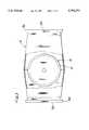
- FIG. 1is a schematic vertical section of a horizontal reactor of the present invention for depositing an epitaxial layer on a semiconductor wafer;
- FIG. 2is a schematic top plan of a reaction chamber of the reactor having parts broken away to show a susceptor positioned in the reaction chamber;
- FIG. 3is a section of the reactor taken in the plane of line 3--3 of FIG. 1, showing a lower heating array
- FIG. 4is a section of the reactor taken in the plane of line 4--4 of FIG. 3;
- FIG. 5is a perspective of a secondary edge reflector of the present invention.
- a horizontal reactor for depositing an epitaxial layer on a semiconductor wafer Wis identified in its entirety by the reference numeral 10.
- the reactoris housed in an enclosure 12 (partially shown) and generally comprises a reaction chamber (generally designated 14), a susceptor (generally designated 16), an upper heating array (generally designated 18), and a lower heating array (generally designated 20).
- the reaction chamber 14is sized and shaped for receiving the semiconductor wafer W.
- the chamber 14extends horizontally between an entrance 30 (FIG. 1) for admitting reactive gas to the chamber and an exit 32 (FIG. 1) for venting reactive gas from the chamber.
- Both the entrance 30 and exit 32have flanges 34, 36, respectively, for releasably connecting the reaction chamber to process piping (not shown) which transports the reactive gas to and from the chamber.
- the wafer Wis preferably inserted and removed from the chamber 14 through the entrance 30 by a robot (not shown) before and after the chemical vapor deposition process.
- the reaction chamber 14 of the preferred embodimentis made of quartz.
- the susceptor 16has a circular recess 40 which forms a generally planar wafer receiving surface in the upper side of the susceptor for receiving the wafer W.
- the susceptor 16is mounted on a shaft 42 which slowly rotates the susceptor during the chemical vapor deposition process to evenly distribute epitaxial material and thermal energy over the surface of the wafer W.
- a conventional three-armed bracket(not shown) may be mounted on the upper end of the shaft for holding the susceptor. The bracket firmly supports the susceptor but only contacts the susceptor at three points to minimize heat transfer between the shaft and susceptor.
- the upper and lower heating arrays 18, 20, respectively,are similar to one another. To eliminate redundancy, only the lower heating array 20 will be described in detail. The minor differences between the arrays 18, 20 will be described following the description of the lower array. Components of the upper array 18 which are similar to components of the lower array 20 are designated by similar numbers in the drawings, but will include a prime symbol to signify that they are upper array components.
- the lower heating array 20comprises eight tubular infrared heat lamps 50 arranged parallel to each other in a plane, four bulb-type infrared heat lamps 52 positioned below the tubular heat lamps, and a primary reflector (generally designated 54) for directing thermal radiation emitted by the heat lamps toward the susceptor 16 to heat the semiconductor wafer W and susceptor.
- the array 20also includes a support structure, generally designated 56, for supporting the primary reflector 54 and heat lamps 50, 52.
- the primary reflector 54includes two parabolic reflectors 58 which lie under the two outermost tubular heat lamps 50 on each side of the array 20, and a flat reflector 60 which lies under the four centrally-located tubular heat lamps.
- Slots 62are formed in the reflector 54 under each tubular heat lamp 50 for permitting cooling air circulation around the lamps.
- a cloverleaf-shaped hole 64is formed in the center of the central reflector 60.
- cylindrical housings 66extend down at an angle from the reflector 60 below each lobe of the hole 64 for holding conventional bulb-type infrared heat lamp assemblies 68.
- the housings 66are angled to direct thermal energy emitted by the bulb-type heat lamps 52 toward a central portion of the susceptor 16.
- the support structure 56is best understood by referring to FIGS. 1, 3 and 4.
- the structure 56comprises two cooling manifolds 80 which underlie the ends of the primary reflector 54.
- Each of the manifolds 80has an internal passage 82 for conveying cooling water to reduce the temperature of the primary reflector 54.
- the manifolds 80are attached to the enclosure 12 with screw fasteners 84 (FIG. 3), and the reflectors 58, 60 are attached to the manifolds with more screw fasteners (not shown).
- a framesurrounds the primary reflector 54 and comprises two end plates 92 (only one of which is visible) and two sheet metal secondary reflectors 94.
- the ends of the end plates 92 and secondary reflectors 94are fastened together by screw fasteners 96 (FIG. 4).
- a cover 98is attached to the end plates 92 with screw fasteners 100 to cover the ends of the tubular heat lamps 50.
- the covers 98, end plates 92 and secondary reflectors 94 of the preferred embodimentare made of aluminum.
- the exterior surfaces of these componentsare polished and gold plated to improve the thermal reflectivity which reduces their temperature and directs thermal energy toward the reaction chamber 14.
- ceramic insulators 102, 104are positioned above and below the ends of the tubular heat lamps 50. Wires 106 extending from each end of the heat lamps 50 are fastened with screws 108 to a bus 110 (FIG. 3) mounted on the insulator 104 for delivering electricity to the heat lamps when energized by a control system (not shown).
- the upper heating array 18(shown in FIGS. 1 and 4) is identical to the lower array 20 except that it holds nine tubular lamps 50' rather than eight, and it does not include bulb-type heat lamps 52 or the associated housings 66. Furthermore, the outer reflectors 58' of the upper heating array 18 are flat rather than parabolic.
- the previously described heating arrays 18, 20are conventional except that the lower side covers have been modified as shown in FIG. 5 to form the secondary reflectors 94, 94'.
- these heating arrays 18, 20are modified Epsilon I Epitaxial Epi reactors manufactured by Advanced Semiconductor Materials America Inc. of Phoenix, Ariz.
- the secondary reflectors 94, 94'extend parallel to the tubular heat lamps 50 so their central portions are positioned beside the primary reflectors 58 and at least partially behind the reflective (i.e., specular) surface of the primary reflectors.
- Each secondary reflector 94, 94'has a specular surface 120 which is angled outward so thermal radiation emitted by the sides of the reflectors 58 and by other components is reflected toward the edge of the susceptor 16.
- the specular surface 120recovers misdirected thermal radiation directed generally away from the susceptor 16 and re-directs the misdirected thermal radiation to an edge of the susceptor to heat the edge.
- the energy reflected by the specular surface 120reduces thermal gradients across the susceptor 16 and semiconductor wafer W to inhibit slip dislocations in the wafer during epitaxial layer deposition.
- the specular surface 120 of the preferred embodimentis substantially planar and lies at an angle with respect to the wafer receiving surface 40 of the susceptor 16.
- the surface 120may lie at an angle of between about 40° and about 80° relative to the wafer receiving surface 40 and the plane of the tubular heat lamps 50.
- the specular surface 120 of the preferred embodimentlies at an angle of about 55° relative to the wafer receiving surface 40 of the susceptor 16 and the plane of the tubular heat lamps 50.
Landscapes
- Chemical & Material Sciences (AREA)
- Metallurgy (AREA)
- Engineering & Computer Science (AREA)
- Materials Engineering (AREA)
- Organic Chemistry (AREA)
- General Chemical & Material Sciences (AREA)
- Chemical Kinetics & Catalysis (AREA)
- Crystallography & Structural Chemistry (AREA)
- Health & Medical Sciences (AREA)
- Toxicology (AREA)
- Mechanical Engineering (AREA)
- Crystals, And After-Treatments Of Crystals (AREA)
- Chemical Vapour Deposition (AREA)
Abstract
Description
Claims (14)
Priority Applications (7)
| Application Number | Priority Date | Filing Date | Title |
|---|---|---|---|
| US08/863,960US5792273A (en) | 1997-05-27 | 1997-05-27 | Secondary edge reflector for horizontal reactor |
| PCT/US1998/007088WO1998054381A1 (en) | 1997-05-27 | 1998-04-08 | Secondary edge reflector for horizontal reactor |
| JP50065599AJP2002500613A (en) | 1997-05-27 | 1998-04-08 | End reflectors for horizontal reactors |
| KR1019997011025AKR20010013049A (en) | 1997-05-27 | 1998-04-08 | Secondary edge reflector for horizontal reactor |
| CN98805543ACN1258324A (en) | 1997-05-27 | 1998-04-08 | Secondary edge reflector for horizontal reactor |
| EP98914635AEP0985060A1 (en) | 1997-05-27 | 1998-04-08 | Secondary edge reflector for horizontal reactor |
| MYPI98002219AMY133778A (en) | 1997-05-27 | 1998-05-19 | Secondary edge reflector for horizontal reactor |
Applications Claiming Priority (1)
| Application Number | Priority Date | Filing Date | Title |
|---|---|---|---|
| US08/863,960US5792273A (en) | 1997-05-27 | 1997-05-27 | Secondary edge reflector for horizontal reactor |
Publications (1)
| Publication Number | Publication Date |
|---|---|
| US5792273Atrue US5792273A (en) | 1998-08-11 |
Family
ID=25342201
Family Applications (1)
| Application Number | Title | Priority Date | Filing Date |
|---|---|---|---|
| US08/863,960Expired - LifetimeUS5792273A (en) | 1997-05-27 | 1997-05-27 | Secondary edge reflector for horizontal reactor |
Country Status (7)
| Country | Link |
|---|---|
| US (1) | US5792273A (en) |
| EP (1) | EP0985060A1 (en) |
| JP (1) | JP2002500613A (en) |
| KR (1) | KR20010013049A (en) |
| CN (1) | CN1258324A (en) |
| MY (1) | MY133778A (en) |
| WO (1) | WO1998054381A1 (en) |
Cited By (21)
| Publication number | Priority date | Publication date | Assignee | Title |
|---|---|---|---|---|
| WO2000026946A1 (en)* | 1998-10-30 | 2000-05-11 | Applied Materials, Inc. | Dual surface reflector |
| US6454863B1 (en)* | 1998-11-19 | 2002-09-24 | Asm America, Inc. | Compact process chamber for improved process uniformity |
| US6476362B1 (en) | 2000-09-12 | 2002-11-05 | Applied Materials, Inc. | Lamp array for thermal processing chamber |
| US6709267B1 (en) | 2002-12-27 | 2004-03-23 | Asm America, Inc. | Substrate holder with deep annular groove to prevent edge heat loss |
| US20050109275A1 (en)* | 2003-11-21 | 2005-05-26 | Wood Eric R. | Reactor chamber |
| US20050166844A1 (en)* | 2004-02-03 | 2005-08-04 | Nicholas Gralenski | High reflectivity atmospheric pressure furnace for preventing contamination of a work piece |
| US20110159214A1 (en)* | 2008-03-26 | 2011-06-30 | Gt Solar, Incorporated | Gold-coated polysilicon reactor system and method |
| US8138451B2 (en) | 1999-01-06 | 2012-03-20 | Mattson Technology, Inc. | Heating device for heating semiconductor wafers in thermal processing chambers |
| EP2409319A4 (en)* | 2009-03-16 | 2013-07-24 | Alta Devices Inc | Heating lamp system and methods thereof |
| CN103805954A (en)* | 2014-02-20 | 2014-05-21 | 江西沃格光电股份有限公司 | Magneto-controlled sputter coating system |
| JP2014514734A (en)* | 2011-03-11 | 2014-06-19 | アプライド マテリアルズ インコーポレイテッド | Off-angle heating of the underside of the substrate using a lamp assembly |
| US20160013079A1 (en)* | 2014-07-11 | 2016-01-14 | Semes Co., Ltd. | Apparatus for treating substrate |
| US20160355947A1 (en)* | 2015-06-05 | 2016-12-08 | Sensor Electronic Technology, Inc. | Susceptor Heating For Epitaxial Growth Process |
| US9957617B2 (en) | 2015-03-30 | 2018-05-01 | Samsung Electronics Co., Ltd. | Deposition system for forming thin layer |
| US10184193B2 (en) | 2015-05-18 | 2019-01-22 | Globalwafers Co., Ltd. | Epitaxy reactor and susceptor system for improved epitaxial wafer flatness |
| US20210104420A1 (en)* | 2019-10-02 | 2021-04-08 | Semes Co., Ltd. | Support unit, substrate treating apparatus including the same, and substrate treating method |
| US11015244B2 (en) | 2013-12-30 | 2021-05-25 | Advanced Material Solutions, Llc | Radiation shielding for a CVD reactor |
| US20210285105A1 (en)* | 2017-10-30 | 2021-09-16 | Applied Materials, Inc. | Multi zone spot heating in epi |
| US20220322492A1 (en)* | 2021-04-06 | 2022-10-06 | Applied Materials, Inc. | Epitaxial deposition chamber |
| WO2023246692A1 (en)* | 2022-06-23 | 2023-12-28 | 江苏天芯微半导体设备有限公司 | Temperature control device and epitaxy apparatus comprising same |
| CN117587506A (en)* | 2024-01-15 | 2024-02-23 | 芯三代半导体科技(苏州)股份有限公司 | Substrate bearing mechanism, tray assembly and silicon carbide epitaxial equipment |
Families Citing this family (6)
| Publication number | Priority date | Publication date | Assignee | Title |
|---|---|---|---|---|
| JP5168788B2 (en)* | 2006-01-23 | 2013-03-27 | 信越半導体株式会社 | Manufacturing method of SOI wafer |
| WO2009085992A2 (en)* | 2007-12-20 | 2009-07-09 | Applied Materials, Inc. | Thermal reactor with improved gas flow distribution |
| FR2930561B1 (en)* | 2008-04-28 | 2011-01-14 | Altatech Semiconductor | DEVICE AND METHOD FOR CHEMICAL TREATMENT IN STEAM PHASE. |
| CN102330147B (en)* | 2010-07-14 | 2015-11-25 | 郭志凯 | A kind of silicon chip produces epitaxial device and system thereof |
| DE102014014970B4 (en) | 2014-10-14 | 2020-01-02 | NICE Solar Energy GmbH | Device and method for measuring the layer thickness for vapor deposition processes |
| CN114686974B (en)* | 2022-03-30 | 2024-11-26 | 上海埃延半导体有限公司 | A reactor for substrate epitaxy |
Family Cites Families (5)
| Publication number | Priority date | Publication date | Assignee | Title |
|---|---|---|---|---|
| JPS5959876A (en)* | 1982-09-30 | 1984-04-05 | Ushio Inc | Operating method of light irradiation furnace |
| US4654509A (en)* | 1985-10-07 | 1987-03-31 | Epsilon Limited Partnership | Method and apparatus for substrate heating in an axially symmetric epitaxial deposition apparatus |
| US4836138A (en)* | 1987-06-18 | 1989-06-06 | Epsilon Technology, Inc. | Heating system for reaction chamber of chemical vapor deposition equipment |
| US5108792A (en)* | 1990-03-09 | 1992-04-28 | Applied Materials, Inc. | Double-dome reactor for semiconductor processing |
| US5467220A (en)* | 1994-02-18 | 1995-11-14 | Applied Materials, Inc. | Method and apparatus for improving semiconductor wafer surface temperature uniformity |
- 1997
- 1997-05-27USUS08/863,960patent/US5792273A/ennot_activeExpired - Lifetime
- 1998
- 1998-04-08WOPCT/US1998/007088patent/WO1998054381A1/ennot_activeApplication Discontinuation
- 1998-04-08JPJP50065599Apatent/JP2002500613A/enactivePending
- 1998-04-08KRKR1019997011025Apatent/KR20010013049A/ennot_activeCeased
- 1998-04-08CNCN98805543Apatent/CN1258324A/enactivePending
- 1998-04-08EPEP98914635Apatent/EP0985060A1/ennot_activeWithdrawn
- 1998-05-19MYMYPI98002219Apatent/MY133778A/enunknown
Cited By (30)
| Publication number | Priority date | Publication date | Assignee | Title |
|---|---|---|---|---|
| US6108491A (en)* | 1998-10-30 | 2000-08-22 | Applied Materials, Inc. | Dual surface reflector |
| WO2000026946A1 (en)* | 1998-10-30 | 2000-05-11 | Applied Materials, Inc. | Dual surface reflector |
| US6869485B2 (en) | 1998-11-19 | 2005-03-22 | Asm America, Inc. | Compact process chamber for improved process uniformity |
| US6454863B1 (en)* | 1998-11-19 | 2002-09-24 | Asm America, Inc. | Compact process chamber for improved process uniformity |
| US20020185062A1 (en)* | 1998-11-19 | 2002-12-12 | Halpin Michael W. | Compact process chamber for improved process uniformity |
| US8138451B2 (en) | 1999-01-06 | 2012-03-20 | Mattson Technology, Inc. | Heating device for heating semiconductor wafers in thermal processing chambers |
| US6476362B1 (en) | 2000-09-12 | 2002-11-05 | Applied Materials, Inc. | Lamp array for thermal processing chamber |
| US6709267B1 (en) | 2002-12-27 | 2004-03-23 | Asm America, Inc. | Substrate holder with deep annular groove to prevent edge heat loss |
| US20050109275A1 (en)* | 2003-11-21 | 2005-05-26 | Wood Eric R. | Reactor chamber |
| US7169233B2 (en) | 2003-11-21 | 2007-01-30 | Asm America, Inc. | Reactor chamber |
| US20050166844A1 (en)* | 2004-02-03 | 2005-08-04 | Nicholas Gralenski | High reflectivity atmospheric pressure furnace for preventing contamination of a work piece |
| US20110159214A1 (en)* | 2008-03-26 | 2011-06-30 | Gt Solar, Incorporated | Gold-coated polysilicon reactor system and method |
| EP2409319A4 (en)* | 2009-03-16 | 2013-07-24 | Alta Devices Inc | Heating lamp system and methods thereof |
| JP2014514734A (en)* | 2011-03-11 | 2014-06-19 | アプライド マテリアルズ インコーポレイテッド | Off-angle heating of the underside of the substrate using a lamp assembly |
| US11015244B2 (en) | 2013-12-30 | 2021-05-25 | Advanced Material Solutions, Llc | Radiation shielding for a CVD reactor |
| CN103805954B (en)* | 2014-02-20 | 2016-01-13 | 江西沃格光电股份有限公司 | Magnetron sputtering coating system |
| CN103805954A (en)* | 2014-02-20 | 2014-05-21 | 江西沃格光电股份有限公司 | Magneto-controlled sputter coating system |
| US10490427B2 (en)* | 2014-07-11 | 2019-11-26 | Semes Co., Ltd. | Apparatus for treating substrate |
| US20160013079A1 (en)* | 2014-07-11 | 2016-01-14 | Semes Co., Ltd. | Apparatus for treating substrate |
| US9957617B2 (en) | 2015-03-30 | 2018-05-01 | Samsung Electronics Co., Ltd. | Deposition system for forming thin layer |
| US10184193B2 (en) | 2015-05-18 | 2019-01-22 | Globalwafers Co., Ltd. | Epitaxy reactor and susceptor system for improved epitaxial wafer flatness |
| US20160355947A1 (en)* | 2015-06-05 | 2016-12-08 | Sensor Electronic Technology, Inc. | Susceptor Heating For Epitaxial Growth Process |
| US20210285105A1 (en)* | 2017-10-30 | 2021-09-16 | Applied Materials, Inc. | Multi zone spot heating in epi |
| US11821088B2 (en)* | 2017-10-30 | 2023-11-21 | Applied Materials, Inc. | Multi zone spot heating in EPI |
| US20210104420A1 (en)* | 2019-10-02 | 2021-04-08 | Semes Co., Ltd. | Support unit, substrate treating apparatus including the same, and substrate treating method |
| US11798822B2 (en)* | 2019-10-02 | 2023-10-24 | Semes Co., Ltd. | Support unit, substrate treating apparatus including the same, and substrate treating method |
| US20220322492A1 (en)* | 2021-04-06 | 2022-10-06 | Applied Materials, Inc. | Epitaxial deposition chamber |
| US12324061B2 (en)* | 2021-04-06 | 2025-06-03 | Applied Materials, Inc. | Epitaxial deposition chamber |
| WO2023246692A1 (en)* | 2022-06-23 | 2023-12-28 | 江苏天芯微半导体设备有限公司 | Temperature control device and epitaxy apparatus comprising same |
| CN117587506A (en)* | 2024-01-15 | 2024-02-23 | 芯三代半导体科技(苏州)股份有限公司 | Substrate bearing mechanism, tray assembly and silicon carbide epitaxial equipment |
Also Published As
| Publication number | Publication date |
|---|---|
| JP2002500613A (en) | 2002-01-08 |
| KR20010013049A (en) | 2001-02-26 |
| CN1258324A (en) | 2000-06-28 |
| EP0985060A1 (en) | 2000-03-15 |
| MY133778A (en) | 2007-11-30 |
| WO1998054381A1 (en) | 1998-12-03 |
Similar Documents
| Publication | Publication Date | Title |
|---|---|---|
| US5792273A (en) | Secondary edge reflector for horizontal reactor | |
| US5418885A (en) | Three-zone rapid thermal processing system utilizing wafer edge heating means | |
| EP0471365B1 (en) | Semiconductor wafer processing apparatus | |
| EP0461194B1 (en) | A high capacity epitaxial reactor | |
| US4823735A (en) | Reflector apparatus for chemical vapor deposition reactors | |
| EP0147967B1 (en) | Induction heated reactor system for chemical vapor deposition | |
| EP0641016A1 (en) | A modified radiant heat source with isolated optical zones | |
| US5618351A (en) | Thermal processing apparatus and process | |
| JPH10241844A (en) | Heating device and heating method | |
| KR20040028647A (en) | Improved lamphead for a rapid thermal processing chamber | |
| NL8602356A (en) | APPARATUS AND METHOD FOR AN AXIAL SYMMETRICAL REACTOR FOR THE CHEMICAL VAPORIZATION. | |
| JPH02299225A (en) | Pressur-resistant heat reactor system for semiconductor processing | |
| JP2004533117A (en) | Substrate support assembly and substrate processing equipment | |
| CN111599722B (en) | Semiconductor process equipment | |
| CN114420585A (en) | Reflector plate group, lamp group module, substrate processing equipment and adjusting method of reflector plate group | |
| US4284867A (en) | Chemical vapor deposition reactor with infrared reflector | |
| KR20210095059A (en) | Semiconductor processing chamber with filament lamps having nonuniform heat output | |
| US7038173B2 (en) | Thermal processing apparatus and thermal processing method | |
| US10932323B2 (en) | Reflector and susceptor assembly for chemical vapor deposition reactor | |
| US20240167194A1 (en) | Reflector unit and film forming apparatus | |
| US4877573A (en) | Substrate holder for wafers during MBE growth | |
| JP4131523B2 (en) | Heatable swivel device | |
| JPH10340777A (en) | Planar heater | |
| WO1985002417A1 (en) | Method and apparatus for chemical vapor deposition | |
| JPH10284569A (en) | Wafer conveyer |
Legal Events
| Date | Code | Title | Description |
|---|---|---|---|
| AS | Assignment | Owner name:MEMC ELECTRONIC MATERIALS, INC., MISSOURI Free format text:ASSIGNMENT OF ASSIGNORS INTEREST;ASSIGNORS:RIES, MICHAEL J.;HELLWIG, LANCE G.;ROSSI, JON A.;REEL/FRAME:008584/0874 Effective date:19970523 | |
| STCF | Information on status: patent grant | Free format text:PATENTED CASE | |
| AS | Assignment | Owner name:MEMC ELECTRONIC MATERIALS, INC., MISSOURI Free format text:TERMINATION OF SECURITY INTEREST;ASSIGNOR:E.ON AG;REEL/FRAME:012263/0944 Effective date:20011113 Owner name:CITICORP USA, INC., DELAWARE Free format text:SECURITY INTEREST;ASSIGNORS:MEMC PASADENA, INC.;PLASMASIL, L.L.C.;SIBOND, L.L.C.;AND OTHERS;REEL/FRAME:012273/0145 Effective date:20011113 Owner name:CITICORP USA, INC., DELAWARE Free format text:SECURITY AGREEMENT;ASSIGNORS:MEMC PASADENA, INC.;PLASMASIL, L.L.C.;SIBOND, L.L.C.;AND OTHERS;REEL/FRAME:012280/0161 Effective date:20011113 | |
| AS | Assignment | Owner name:E. ON AG, GERMANY Free format text:SECURITY INTEREST;ASSIGNOR:MEMC ELECTRONIC MATERIALS, INC.;REEL/FRAME:012407/0806 Effective date:20011025 | |
| AS | Assignment | Owner name:CITICORP USA, INC., DELAWARE Free format text:SECURITY AGREEMENT;ASSIGNORS:MEMC PASADENA, INC.;PLASMASIL, L.L.C.;SIBOND, L.L.C.;AND OTHERS;REEL/FRAME:012365/0345 Effective date:20011221 | |
| FPAY | Fee payment | Year of fee payment:4 | |
| AS | Assignment | Owner name:CITICORP USA, INC., DELAWARE Free format text:SECURITY AGREEMENT;ASSIGNORS:MEMC ELECTRONIC MATERIALS, INC.;MEMC PASADENA, INC.;PLASMASIL, L.L.C.;AND OTHERS;REEL/FRAME:013964/0378;SIGNING DATES FROM 20020303 TO 20030303 Owner name:CITICORP USA, INC., DELAWARE Free format text:SECURITY AGREEMENT;ASSIGNORS:MEMC ELECTRONIC MATERIALS, INC.;MEMC PASADENA, INC.;PLASMASIL, L.L.C.;AND OTHERS;SIGNING DATES FROM 20020303 TO 20030303;REEL/FRAME:013964/0378 | |
| AS | Assignment | Owner name:MEMC ELECTRONIC MATERIALS, INC., MISSOURI Free format text:RELEASE OF SECURITY INTEREST;ASSIGNOR:CITICORP USA, INC.;REEL/FRAME:016641/0045 Effective date:20050602 | |
| FPAY | Fee payment | Year of fee payment:8 | |
| FPAY | Fee payment | Year of fee payment:12 | |
| AS | Assignment | Owner name:BANK OF AMERICA, N.A., MASSACHUSETTS Free format text:SECURITY AGREEMENT;ASSIGNORS:MEMC ELECTRONIC MATERIALS, INC.;SUNEDISON LLC;SOLAICX;REEL/FRAME:026064/0720 Effective date:20110317 | |
| AS | Assignment | Owner name:GOLDMAN SACHS BANK USA, NEW JERSEY Free format text:SECURITY AGREEMENT;ASSIGNORS:NVT, LLC;SUN EDISON LLC;SOLAICX, INC.;AND OTHERS;REEL/FRAME:029057/0810 Effective date:20120928 | |
| AS | Assignment | Owner name:SUN EDISON LLC, CALIFORNIA Free format text:RELEASE BY SECURED PARTY;ASSIGNOR:BANK OF AMERICA, N.A.;REEL/FRAME:031870/0031 Effective date:20131220 Owner name:SUN EDISON LLC, CALIFORNIA Free format text:RELEASE BY SECURED PARTY;ASSIGNOR:GOLDMAN SACHS BANK USA;REEL/FRAME:031870/0092 Effective date:20131220 Owner name:SOLAICX, OREGON Free format text:RELEASE BY SECURED PARTY;ASSIGNOR:GOLDMAN SACHS BANK USA;REEL/FRAME:031870/0092 Effective date:20131220 Owner name:NVT, LLC, CALIFORNIA Free format text:RELEASE BY SECURED PARTY;ASSIGNOR:GOLDMAN SACHS BANK USA;REEL/FRAME:031870/0092 Effective date:20131220 Owner name:SUNEDISON, INC. (F/K/A MEMC ELECTRONIC MATERIALS, Free format text:RELEASE BY SECURED PARTY;ASSIGNOR:BANK OF AMERICA, N.A.;REEL/FRAME:031870/0031 Effective date:20131220 Owner name:ENFLEX CORPORATION, CALIFORNIA Free format text:RELEASE BY SECURED PARTY;ASSIGNOR:BANK OF AMERICA, N.A.;REEL/FRAME:031870/0031 Effective date:20131220 Owner name:SOLAICX, OREGON Free format text:RELEASE BY SECURED PARTY;ASSIGNOR:BANK OF AMERICA, N.A.;REEL/FRAME:031870/0031 Effective date:20131220 Owner name:SUNEDISON, INC. (F/K/A MEMC ELECTRONIC MATERIALS, Free format text:RELEASE BY SECURED PARTY;ASSIGNOR:GOLDMAN SACHS BANK USA;REEL/FRAME:031870/0092 Effective date:20131220 | |
| AS | Assignment | Owner name:DEUTSCHE BANK AG NEW YORK BRANCH, NEW JERSEY Free format text:SECURITY AGREEMENT;ASSIGNORS:SUNEDISON, INC.;SOLAICX;SUN EDISON, LLC;AND OTHERS;REEL/FRAME:032177/0359 Effective date:20140115 | |
| AS | Assignment | Owner name:NVT, LLC, MARYLAND Free format text:RELEASE BY SECURED PARTY;ASSIGNOR:DEUTSCHE BANK AG NEW YORK BRANCH;REEL/FRAME:032382/0724 Effective date:20140228 Owner name:SUNEDISON, INC., MISSOURI Free format text:RELEASE BY SECURED PARTY;ASSIGNOR:DEUTSCHE BANK AG NEW YORK BRANCH;REEL/FRAME:032382/0724 Effective date:20140228 Owner name:SUN EDISON LLC, CALIFORNIA Free format text:RELEASE BY SECURED PARTY;ASSIGNOR:DEUTSCHE BANK AG NEW YORK BRANCH;REEL/FRAME:032382/0724 Effective date:20140228 Owner name:SOLAICX, OREGON Free format text:RELEASE BY SECURED PARTY;ASSIGNOR:DEUTSCHE BANK AG NEW YORK BRANCH;REEL/FRAME:032382/0724 Effective date:20140228 | |
| AS | Assignment | Owner name:MEMC SOUTHWEST INC., MISSOURI Free format text:RELEASE OF SECURITY INTEREST TO REEL/FRAME: 012280/0161;ASSIGNOR:CITICORP USA, INC.;REEL/FRAME:032458/0794 Effective date:20140313 Owner name:PLASMASIL, L.L.C., MISSOURI Free format text:RELEASE OF SECURITY INTEREST TO REEL/FRAME: 012280/0161;ASSIGNOR:CITICORP USA, INC.;REEL/FRAME:032458/0794 Effective date:20140313 Owner name:MEMC PASADENA, INC., TEXAS Free format text:RELEASE OF SECURITY INTEREST TO REEL/FRAME: 012280/0161;ASSIGNOR:CITICORP USA, INC.;REEL/FRAME:032458/0794 Effective date:20140313 Owner name:MEMC INTERNATIONAL, INC. (NOW KNOWN AS SUNEDISON I Free format text:RELEASE OF SECURITY INTEREST TO REEL/FRAME: 012280/0161;ASSIGNOR:CITICORP USA, INC.;REEL/FRAME:032458/0794 Effective date:20140313 Owner name:MEMC ELECTRONIC MATERIALS, INC. (NOW KNOWN AS SUNE Free format text:RELEASE OF SECURITY INTEREST TO REEL/FRAME: 012280/0161;ASSIGNOR:CITICORP USA, INC.;REEL/FRAME:032458/0794 Effective date:20140313 Owner name:SIBOND, L.L.C., MISSOURI Free format text:RELEASE OF SECURITY INTEREST TO REEL/FRAME: 012280/0161;ASSIGNOR:CITICORP USA, INC.;REEL/FRAME:032458/0794 Effective date:20140313 | |
| AS | Assignment | Owner name:SUNEDISON SEMICONDUCTOR LIMITED (UEN201334164H), S Free format text:ASSIGNMENT OF ASSIGNORS INTEREST;ASSIGNOR:MEMC ELECTRONIC MATERIALS, INC.;REEL/FRAME:033023/0430 Effective date:20140523 | |
| AS | Assignment | Owner name:SUNEDISON SEMICONDUCTOR TECHNOLOGY PTE. LTD., MISS Free format text:NOTICE OF LICENSE AGREEMENT;ASSIGNOR:SUNEDISON SEMICONDUCTOR LIMITED;REEL/FRAME:033099/0001 Effective date:20140527 |