US5790612A - System and method to reduce jitter in digital delay-locked loops - Google Patents
System and method to reduce jitter in digital delay-locked loopsDownload PDFInfo
- Publication number
- US5790612A US5790612AUS08/609,068US60906896AUS5790612AUS 5790612 AUS5790612 AUS 5790612AUS 60906896 AUS60906896 AUS 60906896AUS 5790612 AUS5790612 AUS 5790612A
- Authority
- US
- United States
- Prior art keywords
- signal
- delay
- circuit
- source signal
- source
- Prior art date
- Legal status (The legal status is an assumption and is not a legal conclusion. Google has not performed a legal analysis and makes no representation as to the accuracy of the status listed.)
- Expired - Lifetime
Links
Images


Classifications
- H—ELECTRICITY
- H03—ELECTRONIC CIRCUITRY
- H03K—PULSE TECHNIQUE
- H03K5/00—Manipulating of pulses not covered by one of the other main groups of this subclass
- H03K5/13—Arrangements having a single output and transforming input signals into pulses delivered at desired time intervals
- H03K5/131—Digitally controlled
- H—ELECTRICITY
- H03—ELECTRONIC CIRCUITRY
- H03K—PULSE TECHNIQUE
- H03K5/00—Manipulating of pulses not covered by one of the other main groups of this subclass
- H03K5/13—Arrangements having a single output and transforming input signals into pulses delivered at desired time intervals
- H03K5/133—Arrangements having a single output and transforming input signals into pulses delivered at desired time intervals using a chain of active delay devices
- H—ELECTRICITY
- H03—ELECTRONIC CIRCUITRY
- H03L—AUTOMATIC CONTROL, STARTING, SYNCHRONISATION OR STABILISATION OF GENERATORS OF ELECTRONIC OSCILLATIONS OR PULSES
- H03L7/00—Automatic control of frequency or phase; Synchronisation
- H03L7/06—Automatic control of frequency or phase; Synchronisation using a reference signal applied to a frequency- or phase-locked loop
- H03L7/08—Details of the phase-locked loop
- H03L7/081—Details of the phase-locked loop provided with an additional controlled phase shifter
- H03L7/0812—Details of the phase-locked loop provided with an additional controlled phase shifter and where no voltage or current controlled oscillator is used
- H03L7/0814—Details of the phase-locked loop provided with an additional controlled phase shifter and where no voltage or current controlled oscillator is used the phase shifting device being digitally controlled
- H—ELECTRICITY
- H03—ELECTRONIC CIRCUITRY
- H03L—AUTOMATIC CONTROL, STARTING, SYNCHRONISATION OR STABILISATION OF GENERATORS OF ELECTRONIC OSCILLATIONS OR PULSES
- H03L7/00—Automatic control of frequency or phase; Synchronisation
- H03L7/06—Automatic control of frequency or phase; Synchronisation using a reference signal applied to a frequency- or phase-locked loop
- H03L7/08—Details of the phase-locked loop
- H03L7/081—Details of the phase-locked loop provided with an additional controlled phase shifter
- H03L7/0812—Details of the phase-locked loop provided with an additional controlled phase shifter and where no voltage or current controlled oscillator is used
- H03L7/0816—Details of the phase-locked loop provided with an additional controlled phase shifter and where no voltage or current controlled oscillator is used the controlled phase shifter and the frequency- or phase-detection arrangement being connected to a common input
Definitions
- the present inventionrelates generally to clock synchronization in digital systems. More particularly, the present invention relates to a system and method to reduce phase offset and jitter in digital delay-locked loops.
- Digital designersmust often distribute a centralized clock signal to many components of a system. In high speed digital systems, however designers must overcome the problem of clock skew that the clock signal encounters upon its distribution. Clock skew is the difference in clock timing as seen by different loads that comprise the distribution load of a centralized clock. Clock skew includes static phase offset. To overcome the skew problem, designers employed digital delay-locked loops (DLLs). Digital DLLs are used to phase align the centralized clock signal input with a feedback input. The feedback input is generally a version of the centralized clock signal input that has been subjected to a delay substantially equal to that caused by the distribution load on the centralized clock signal.
- DLLsdigital delay-locked loops
- the lock-and-leave solutionhas proven to be only a partial solution to the clock distribution design which attempts to achieve low clock jitter and low clock skew. It performs adequately in well controlled environments, that is, those environments characterized by small fluctuations in temperature (less than 40° C.) or voltage. Such environments generally exist in large systems that have dedicated facilities for their operation. In well controlled environments, parameters affecting clock skew stabilize, and the input clock signal does not tend to drift after the initial lock.
- Trackinggenerally involves increasing or decreasing the delay of a buffered version of the output clock signal to phase align the buffered version of the output clock signal with the centralized clock signal.
- Conventional digital DLLsincorporate multiplexers to switch a clock signal having a desired delay to become the output clock signal. Using multiplexers to switch in a different delay clock signal results in undesirable glitches in the resulting clock signal.
- Deglitching circuitssometimes called synchronizers, are employed in conventional systems to solve the deglitching problem.
- An example deglitching circuitis illustrated in U.S. Pat. No. 5,036,528, Self-Calibrating Clock Synchronizing Scheme, to Costentino et al.
- the present inventionincorporates a variable delay circuit to add delay to a clock signal.
- a coarse delayis determined and fixed by a circuit employing the concept of a lock-and-leave circuit.
- the present inventioneffectively fine tunes the coarse delay fixed by the lock-and-leave circuit.
- VDEsvariable delay elements
- the rate at which the fine tune circuit is updatedis determined by N mode bits. Accordingly, there are 2 N possible update rates.
- the N mode bitsare input to a control circuit.
- the control circuitexecutes an update sequence. At the completion of the update sequence, the control lines of the variable delay elements have been adjusted to either increase or decrease the amount of delay present in the clock path for skew compensation.
- Control lineswhich are bussed to each VDE, set the propagation delay of all the VDEs, thereby controlling the amount of delay inserted into the clock path.
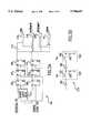
- FIG. 1illustrates a tracking circuit 100 having a user controllable tracking rate according to a preferred embodiment of the present invention.
- FIG. 2illustrates a variable delay element 102 according to a preferred embodiment of the present invention.
- FIG. 3Aillustrates a phase detector 104 according to a preferred embodiment of the present invention.
- FIG. 3Billustrates a circuit 313 used by the phase detector to delay a clock signal.
- FIG. 3Cillustrates the relationship between inputs to phase detector 104.
- FIG. 3Dillustrates the outputs of phase detector 104 in tabular form.
- FIG. 4Aillustrates control circuit 106 according to a preferred embodiment of the present invention.
- FIG. 4Bis a tracking state diagram, implemented by a tracking state machine 404, according to a preferred embodiment of the present invention.
- FIG. 4Cis a tracking divisor/update circuit 406 according to a preferred embodiment of the present invention.
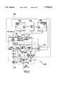
- FIG. 5is a variable tracking delay lock loop 500 according to a preferred embodiment of the present invention.
- FIG. 6illustrates a transistor layout for a delay line 504 according to a preferred embodiment of the present invention that is implemented using gate array technology.
- the present inventionincorporates a variable delay circuit to add delay to a clock signal.
- a coarse delayis determined and fixed by a circuit employing the concept of a lock-and-leave circuit.
- the present inventioneffectively fine tunes the coarse delay determined by the lock-and-leave circuit.
- the tracking circuit 100includes a variable delay circuit 102, a phase detector 104, and control circuit 106.
- the variable delay circuit 102inputs a source signal 130 on line 110.
- the source signal 130is the output of the lock-and-leave delay circuit (described below with reference to FIG. 5).
- the variable delay circuit 102inputs delay control signals over delay control bus 134. In the preferred embodiment, there are 3 control signals for each variable delay element (discussed below) in the variable delay circuit 102.
- the delay control signals carried by delay control bus 134control the amount of delay that the variable delay circuit 102 inserts into clock signal paths 136 and 137.
- the variable delay circuit 102outputs a delayed clock signal 136 on line 122. This signal is also the output clock signal 137 of the variable delay circuit 102.
- the output clock signal 137is used to clock distributed loads in a system (not shown) that uses a centralized clock.
- the phase detector 104inputs the delayed clock signal 136 from line 122.
- the phase detector 104also inputs a source signal 130 over line 112.
- the "source signal 130”is alternately referred to as the "source clock signal 130.”
- the phase detector 104compares the phase of the source signal 130 to the phase of the delayed clock signal 136 to determine whether the phase of the delayed clock signal 136 leads, lags, or is in phase with the phase of the source signal 130.
- phase detector 104determines that the phase of the delayed clock signal 136 leads the phase of the source signal 130, the system must increase the amount of delay of the delayed clock signal 136 to achieve phase lock. Thus, the phase detector 104 informs the control circuit 106 to increment the delay of the variable delay circuit 102. This is accomplished by sending an increment signal 138 over line 114.
- phase detector 104determines that the phase of the delayed clock signal 136 lags the phase of the source signal 130, the system must decrease the delay of the delayed clock signal 136 to achieve phase lock. Thus, the phase detector 104 informs the control circuit 106 to decrement the delay of the variable delay circuit 102. This is accomplished by sending a decrement signal 140 over line 116.
- phase detector 104determines that the phase of the delayed clock signal 136 is in phase with the phase of the source signal 130, the system does not modify the delay of the delayed clock signal 136. This is accomplished by sending a lock signal 142 over line 118. The generation of increment signal 138, decrement signal 140, and lock signal 142 is described below.
- the control circuit 106inputs the increment signal 138, decrement signal 140, and lock signal 142 generated by the phase detector 104.
- the control circuit 106also inputs one or more mode select bits 144 that corresponds to a user selectable tracking rate.
- the user selectable tracking rateis the rate at which the present invention updates the variable delay circuit 102.
- the control circuit 106outputs delay control signals on delay control bus 134 to increment, decrement, or not modify the delay of the variable delay element 102. To vary the tracking rate, the control circuit 106 outputs delay control signals on delay control bus 134 at varying times corresponding to a tracking update rate indicated by the mode select bits 144 over line 124.
- Two mode select bits 144are used in the preferred embodiment of the present invention.
- the two mode select bits 144indicate whether slow, medium, fast, or no tracking is desired. It would be apparent to those skilled in the art how to design and implement a decoder that selects a tracking mode in accordance with two input mode bits. Further, it would be apparent to those skilled in the art to increase the number of mode bits to provide for more tracking states.
- variable delay circuit 102comprises a plurality of M variable delay elements (VDEs) 250a, 250b, . . . 250m connected in series.
- VDEsvariable delay elements
- Mcan be an even number in order to avoid outputting a delayed, but inverted, representation of an input signal, IN.
- VDEs 250a, 250b, . . . 250mare illustrated in FIG. 2.
- VDE 250aOnly the VDE 250a is described below. Each of the remaining M-1 VDEs 250b, . . . 250m, however, operates in a substantially the same manner to the VDE 250a.
- Each VDE 250acomprises a CMOS inverter 258.
- the CMOS inverter 258comprises a PMOS pull-up transistor 240 and an NMOS pull-down transistor 242. Coupled to each PMOS pull-up transistor 240 are transistors 220, 222, and 224. Transistors 220, 222, and 224 are connected in parallel. Coupled to each NMOS pull-down transistor 242 are transistors 226, 228, and 230. Transistors 226, 228, and 230 are connected in parallel. Transistors 220, 222, 224, 226, 228, and 226 are controlled by delay control bus signals on lines 202, 204, 206, 208, 210, and 212 respectively. It would be apparent to those skilled in the art that lines 202, 204, 206, 208, 210, and 212 comprise the delay control bus 134.
- the delay control bus signalsare generated by the control circuit 106 as described above.
- control signals supplied to each VDEthere are 3 control signals supplied to each VDE in the preferred embodiment of the current invention. It would be apparent to those skilled in the art that a fewer or a greater number of control signals can be applied to the VDEs as required by a particular implementation of the present invention. For example, by supplying an independent control signal to transistors 226, 228, and 230 on lines 208, 210, and 212 respectively, the pull down characteristics of the CMOS inverter 258 can be controlled independently of the pull-up characteristics.
- the effective resistance of the transistors 220, 222, 224is modulated to alter the pull-up time for the pull-up transistor 240 of the CMOS inverter 258.
- the effective resistance of the transistors 226, 228, and 230is modulated to alter the pull-down time for the pull-down transistor 242 of the CMOS inverter 258. The modulation is performed such that the incremental resistance change is small. By keeping the incremental resistance changes small, the likelihood of undesirable glitches in the circuit is significantly reduced.
- the size of the transistorsis chosen to control the range of the effective resistance.
- the transistors 220, 222, 224have different sizes. It would be apparent to those skilled in the art that transistors of different sizes can be used to realize the variable delay described above.
- control signals on the control bus 134allow for other combinations of the transistors. Such other combinations allow for different delays to be added to the IN signal, i.e., the SOURCE signal 130.
- the middle-sized transistorcan be the transistor that is always on. To achieve less delay, the next smallest transistor can be added. To achieve even less delay, the largest transistor is added.
- each VDEis set such that a minimal number of the delay control transistors remain active to maintain VDE operation.
- the minimal number of active delay control transistorscorresponds to the maximum propagation delay of a VDE at a particular process, control, and temperature.
- the minimal propagation delay of the VDEis achieved for a given process, voltage, and temperature operator point. This causes a change in the delay that the signal experiences through each VDE 250a, 250b, . . . 250m because an RC time constant, inherent in each VDE, changes.
- the time required for the delay element to pull the input signal up to V dd or down to groundchanges. How much delay is added depends on the number of transistors 220, 222, 224, 226, 228, and/or 230 that are turned on.
- the period of the clock signalis not changed other than for the cycle or cycles in which delay is added.
- the capacitive loading offered by the gates of the delay control transistors on the delay control signals on delay control bus 134prevents a rapid transition of the signal voltages.
- there is a slow voltage transition at the gate of the delay control transistorse.g., transistors 220, 222, and 224.
- the slow voltage transition at the gates of the delay control transistorsprevents a rapid turn-on of the delay control transistors, and produces a gradual change between the transistor inactive to active state.
- the gradual switchingavoids undesirable clock signal glitches by spreading the transition from one delay value to another over a period of time that is much greater than the edge rate (i.e., rise and fall times) of the clock signal.
- a phase detector 104determines the relative phase difference between a SYSOUTCLK signal 301 and a SOURCE CLOCK signal 130.
- the SYSOUTCLK signal 301is the delayed clock signal 136.
- the SOURCE CLOCK signal 303is a general reference clock signal having a phase to which a digital DLL tries to align delayed clock signal 136. Such a digital DLL is illustrated in and described later with respect to FIG. 5.
- the phase detector 104determines whether the SYSOUTCLK signal 301 and the SOURCE CLOCK signal 130 are in phase to within a predetermined window or delay.
- the window, or delayaccounts for the unavoidable delay caused by process and metal delays that are inherent in a chip fabrication process.
- the predetermined delayis generated by the SOURCE CLOCK delay circuit 313.
- the window and the SOURCE CLOCK delay circuit 313are described in detail below.
- the phase detector 104 of the preferred embodiment of the present inventioncomprises six D-type flip-flops 302, 304, 306, 308, 310, and 312.
- Flip-flops 304, 306, 308, 310, and 312input the SOURCE CLOCK signal 130 as their input clock.
- Flip-flop 302inputs a delayed version of the SOURCE CLOCK signal 130 as its input clock.
- the phase detector 104is able to determine whether the SYSOUTCLK signal 301 and the SOURCE CLOCK signal 303 are in phase with one another to within a resolution amount.
- the resolution amountis determined by the amount of delay introduced to the SOURCE CLOCK 130 signal by the SOURCE CLOCK delay circuit 313.
- the phase detector 104indicates a lock condition when flip-flop 306 outputs a logic level 1 and flip-flop 312 outputs a logic level 0.
- the lock conditionis determined by a NOR gate 316.
- the phase detector 104indicates that the phase of SYSOUTCLK 301 leads the phase of the SOURCE CLOCK signal 303 when flip-flop 306 outputs a logic level 1 and flip-flop 312 outputs a logic level 1.
- An AND gate 320indicates the condition where the phase of the SYSOUTCLK signal 301 leads the phase of the SOURCE CLOCK signal 303.
- the phase detector 104outputs an increment signal to increase the delay of the SYSOUTCLK signal 301.
- the phase detector 104indicates that the phase of the SYSOUTCLK signal 301 lags the phase of the SOURCE CLOCK signal 303 when flip-flop 306 outputs a logic level 0 and flip-flop 312 outputs a logic level 0.
- a NOR gate 318indicates the condition where the phase of the SYSOUTCLK signal 301 lags the phase of the SOURCE CLOCK signal 303. When the NOR gate 318 detects that the SYSOUTCLK signal 301 lags the SOURCE CLOCK signal 303, the phase detector 104 outputs a decrement signal to decrease the delay of the SYSOUTCLK signal 301.
- flip-flop 306outputs a logic level 0 and flip-flop 312 outputs a logic level 1 is an illegal condition according to the preferred embodiment of the present invention.
- a NOR gate 321detects the illegal state. If the NOR gate 321 detects the illegal state, the phase detector 104 outputs an error signal. In a preferred embodiment of the present invention, the error signal is used to alert a system operator of an error condition in the clock synchronization system.
- phase detector 104can be implemented in a variety of ways. For example, only flip-flops 302 and 308 are required in order to generate the lock, lead, lag, and error signals.
- the phase detector 104 illustrated in FIG. 2provides a more stable solution with improved MTBF due to metastability in flip-flops than a phase detector implementing fewer flip-flops.
- FIG. 3Billustrates a SOURCE CLOCK delay circuit 313 for delaying the SOURCE CLOCK signal 303.
- a tap in delay line 504comprises two inverters. To generate the desired delay, the output of each inverter is applied to a resistor-capacitor (RC) circuit 333, 335.
- RCresistor-capacitor
- Each RC circuit 333, 335has an associated RC time constant.
- the RC time constantdetermines the delay of a signal through the RC circuit 333, 335.
- the aggregate RC time constant through the SOURCE CLOCK delay circuit 313determines the SOURCE CLOCK signal 303 delay.
- the resistoris implemented as an N-channel pass transistor 332.
- the capacitoris implemented as an N-channel capacitor (oxide). Implementing the RC circuit with an N-channel pass transistor and an N-channel capacitor (oxide) has the circuit advantage of more closely tracking the intrinsic inverter delay than does an RC circuit implemented with either metal or polysilicon.
- FIG. 3Cillustrates the relationship between the SYSOUTCLK signal 301 and the delayed version of the SOURCE CLOCK signal 303.
- the phase detector 104determines the relationship as described above.
- SYSOUTCLK signal 301goes to logic level 1 in lead region 350, it leads the SOURCE CLOCK signal 303. In this case flip-flops 306 and 312 each output a logic level 1. This indicates that the delay of the SYSOUTCLK signal 301 must be increased to achieve phase lock.
- SYSOUTCLK signal 301goes to logic level 1 in lock region 352, it is in phase with the SOURCE CLOCK signal 303.
- flip-flop 306outputs a logic level 1 and flip-flop 312 outputs a logic level 0.
- the SYSOUTCLK signal 301goes to logic level 1 in lag region 354, it lags the SOURCE CLOCK signal 303.
- flip-flops 306 and 312each output a logic level 0. This indicates that the delay of the SOURCE CLOCK signal 303 must be reduced to achieve phase lock.
- the lead (decrement), lock, lag (increment) and error conditionsare indicated in tabular form in FIG. 3D.
- the SOURCE CLOCK delay circuit 313determines the width of a lock region 352.
- the widthcan be thought of as a window 340 or delay in which the input of the phase detector 104 are considered to be in phase.
- the window size of window 340is determined by the worst case process delay and metal delay inherent in the fabrication of a chip implementing the present invention. A 50% delay is used in the preferred embodiment of the present invention.
- the SOURCE CLOCK delay circuit 313must delay the SOURCE CLOCK signal 303 by a delay that is greater than a tap delay of a delay line 504, i.e., the resolution of delay line 504. If the SOURCE CLOCK delay circuit 313 delays the SOURCE CLOCK signal 303 by a delay that is smaller than the incremental delay of a tap in delay line 504, the phase detector 104 could not be guaranteed to achieve a lock condition. This is because the width of the lock region 352 would be too small to ensure that a delayed clock signal will eventually fall into the lock region 352.
- the control circuit 106comprises a decoder/counter circuit 402, a tracking state machine 404, and a tracking divisor/update circuit 406.
- the decoder/counter circuit 402comprises a decoder (not shown) and a counter (not shown).
- a decoder and counter for the preferred embodiment of the present inventioncan be constructed in a well known manner.
- the decoder/counter circuit 402inputs increment control 412 and decrement control 414 from the tracking state machine 404.
- the increment control 412increments the count of the counter in the decoder/counter circuit 402.
- the decrement control 414decrements the count of the counter in the decoder/counter circuit 402.
- the output of the counter in the decoder/counter circuit 402is decoded to generate the delay control signals.
- the delay control signalsare transmitted to the variable delay circuit 102 by the delay control bus 134.
- the delay control signals on delay control bus 134are output to the variable delay circuit 102 to control the amount of delay into the source clock signal 130.
- the tracking state machine 404inputs increment signal 138, decrement signal 140, and lock signal 142 from the phase detector 102.
- the tracking state machineoutputs control signals, increment control 412 and decrement control 414, to the decoder/counter circuit 402.
- the tracking state machine 404outputs the signals only when it determines that an update should occur. It determines that an update should occur when the tracking divisor/update circuit 406 asserts a track enable signal 410 (the generation of which is described below with reference to FIG. 4C). If the tracking divisor/update circuit 406 does not assert a track enable signal 410, the tracking state machine 404 does not output the increment signal 412 or decrement signal 414 to the decoder/counter 402.
- the rate at which the tracking state machine 404 is allowed to update the VDEsis determined by the rate that the track enable signal 410 is asserted by the tracking divisor/update circuit 406.
- the rate at which the tracking divisor/update circuit 406 asserts the track enable signal 410is determined by the mode select signal 144.
- the actual assertion rateis a multiple of the source clock period, which is determined by the mode select signal 144.
- the present inventionis an enhancement of the lock-and-leave concept.
- the lock-and-leave circuitprovides a coarse phase lock, while the variable delay element 102 fine tunes the coarse phase lock.
- a lock found signal 418is input to the tracking state machine 404 by a lock-and-leave state machine 508 (described below with reference to FIG. 5).
- the lock found signal 418indicates that the lock-and-leave circuit has found a coarse lock. Only then does the present invention try to fine tune lock.
- the lock signal 142has two purposes. It first determines whether the lock-and-leave circuit has achieved lock. Once this occurs, the lock found 418 signal is asserted. Thereafter, the lock signal 142 is an indication of whether the variable delay element 102 has added sufficient delay to align the phase of the source clock signal 130 and delayed source clock signal 136.
- FIG. 4Billustrates the state diagram implemented by the state machine 404 of a preferred embodiment present invention.
- the "*"indicates signal negation.
- the tracking state machine 404begins in reset state 430.
- the reset statemay be entered upon system startup or assertion of a reset mode signal 422.
- the tracking state machine 404then enters "no track” state 432.
- the variable delay circuit 100does not track in the "no track” state 432.
- the tracking state machine 404remains in the "no track” state 432 until a track enable signal 410 is generated by tracking divisor/update circuit 406 or the lock found signal 418 is asserted.
- the tracking state machine 404Upon the assertion of the track enable signal 410 or the lock found signal 418, the tracking state machine 404 enters "track" state 434. The tracking state machine 404 remains in the “track” state while the phase detector 102 indicates a lock condition, or the system is not allowed to track even though tracking is enabled. The tracking state machine 404 returns to the "no track” state 432 if the track enable signal 410 is deasserted. If the lock signal 138 is asserted indicating the phase detector 104 has achieved lock and the system can track, the tracking state machine 404 determines whether the phase of the SYSOUTCLK signal 301 is too high or too low.
- the tracking state machine 404determines that the phase of the SYSOUTCLK signal 301 is too high when the phase detector 104 asserts the increment signal 140.
- the tracking state machine 404determines that the phase of the SYSOUTCLK signal 301 is too low when the phase detector 104 asserts the decrement signal 138.
- the tracking state machine 404determines that the phase of the SYSOUTCLK signal 301 is too high, the tracking state machine 404 enters state 438. In state 438, the tracking state machine 404 outputs an increment signal 412 that causes the counter in the decoder/counter circuit 402 to increment.
- the tracking state machine 404determines that the phase of the SYSOUTCLK signal 301 is too low, the tracking state machine 404 enters state 436. In state 436, the tracking state machine 404 outputs an decrement signal 414 that causes the counter in the decoder/counter circuit 402 to decrement.
- the tracking state machine 404After the tracking state machine 404 outputs the appropriate control signals, it enters a series of wait states, wait1 440, wait2 442, and wait3 444. Wait states 440, 442, and 444 allow the desired control changes to propagate through the system prior to initiating a new tracking update sequence. Upon completion of the wait3 state 444, the tracking state machine returns to track state 434.
- the tracking divisor/update circuit 406determines the rate of update for the variable delay circuit 102.
- the rate of updateis user selectable. According to a preferred embodiment of the present invention, the selected mode is indicated by mode select bits 144.
- Tracking divisor/update circuit 406outputs a track enable signal 410.
- the track enable signal 410allows the tracking state machine 404 to cause delay control signals on delay control bus 134 to update the delay of the variable delay element 102.
- FIG. 4Cillustrates a tracking divisor/update circuit 406 according to a preferred embodiment of the present invention.
- the tracking divisor/update circuit 406decodes mode select bits 144 using decoder 450.
- the design of a decoder 450 to accomplish this decodingis well-known in the art.
- the update statesare no tracking, slow tracking, medium tracking, and fast tracking.
- the decoder 450asserts one of a no tracking signal 466, a slow tracking signal 464, a medium tracking signal 462, and a fast tracking signal 460.
- a clock divider circuit 452inputs the source signal 130.
- the clock divider circuitimplements a divider circuit to divide the source clock signal 451. Divider circuits are well known in the art.
- the clock divider circuit 452outputs a divided down clock corresponding to each of the update rates that a user can select via mode select 144. In the preferred embodiment of the present invention, the clock divider circuit 452 outputs a slow update clock 468, a medium update clock 470, and a fast update clock 472.
- the clock divider circuit output clock signals 468, 470, and 472are input to track enable signal generation circuit 482.
- the track enable signal generation circuit 482comprises AND gates 454, 456, and 458; and OR gate 479.
- AND gates 454, 456 and 458output (enable) their respective input clock signal 468, 470, or 472 if the decoder 452 asserts their respective control signal 464, 462, or 460.
- the AND gates 454, 456, and 458output no clock signal if the decoder asserts the no track signal 466.
- the OR gate 479passes whichever clock signal 468, 470, or 472 is enabled by AND gates 454, 456, and 458.
- the enabled clock signalis the track enable signal 410. Note that no clock signal is enabled if no track signal 466 is asserted.
- variable tracking digital delay-locked loop 500implements a preferred embodiment of the present invention.
- the variable tracking digital delay-locked loop 500comprises the tracking circuit 100 and a lock-and-leave circuit 502.
- the lock-and-leave circuit 502achieves a coarse lock.
- the tracking circuit 100adds additional delay to fine tune the coarse lock achieved by the lock-and-leave circuit 502 if tracking is enabled.
- the output of the variable tracking digital delay-locked loop 500is output signal 138. If tracking is not enabled, the variable tracking delay locked loop 500 outputs a clock signal delay adjusted by only the coarse amount determined by the lock-and-leave circuit 502.
- the lock-and-leave circuit 502comprises a lock-and-leave state machine 508, and counter 510, three multiplexers 503, 506, 512, and a delay line 504.
- the lock-and-leave state machine 508controls the operation of the lock-and-leave circuit 502.
- the lock-and-leave state machine 508determines when the system has achieved a coarse lock.
- the lock-and-leave state machine 508determines coarse lock by incrementing counter 510 through all of its count states, or until lock is achieved. If lock is not achieved, an error 518 is indicated.
- the counter 510has 2 N count states where N is the number of bits in the counter.
- counter 510is a seven-bit counter. Therefore, the counter 510 has 128 count states.
- the lock-and-leave state machinecycles the counter through its 128 states, or until lock is achieved. Each state corresponds to a different delay in the delay line 504.
- the phase detector 104detects when the variable tracking delay locked loop 500 achieves lock. If the phase detector 104 indicates that the variable digital delay-locked loop 500 has not yet achieved lock, the lock-and-leave state machine 508 causes the counter 510 to increment to the next delay in delay line 504. If the phase detector 104 asserts the lock signal 142, indicating that the variable tracking digital delay-locked loop 500 has achieved phase lock, the lock-and-leave state machine 508 causes the counter 510 to stop counting. At this point the variable tracking digital delay-locked loop 500 has achieved a coarse lock. The lock-and-leave state machine 508 causes the counter 510 value to remain constant until the variable tracking digital delay-locked loop 500 is restarted or reset. The variable tracking digital delay-locked loop 500 is reset by asserting the reset mode 422 signal. This causes the lock-and-leave state machine 508 to generate a reset control signal 516 to reset counter 510.
- the delay line 504comprises a plurality of CMOS inverters. An output from each inverter is input to one of two multiplexers 503 or 506. The output from a non-inverting pair of CMOS inverters (i.e., even pairs) are input to multiplexer 506. The output from inverting pairs of CMOS inverters (i.e., odd pairs) are inputs to multiplexer 503.
- This techniqueincreases the resolution of the delay line by conceptually splitting the delay line into two delay lines, wherein one delay line is offset from the other by an amount less than an inverter delay.
- CMOS invertersthere are 128 CMOS inverters. Sixty-four of the outputs are input to multiplexer 506 (even inverter pairs). The remaining pairs (odd inverter pairs) are input to multiplexer 503. Bits 5-0 of counter 510 are used as select inputs by the multiplexers 503 and 506. Bit 6 of the counter 510 is used as the input select to multiplexer 512. The input select selects between the outputs of multiplexers 503 and 506. For counts 0-63, multiplexer 512 selects the output of multiplexer 506. For counts 64-127, multiplexer 512 selects the output of multiplexer 503.
- ASICapplication specific integrated circuit
- the delay line 504comprises a plurality of taps. Each tap is a CMOS inverter pair.
- the pull-down transistor in a CMOS inverteris generally an NMOS device. Electrons carry the current in an NMOS device.
- the pull-up transistor in a CMOS inverteris generally a PMOS device. Holes carry the current in a PMOS device. Holes are about twice the size of an electron. Thus, the transistor channel in a PMOS device must be approximately twice the width of a corresponding channel of an NMOS device to get the same current flow.
- ASICsdo not generally allow designers to change the width of devices. Thus, ASIC designers generally use two PMOS devices for the pull-up transistor and one NMOS device for the pull-down transistor. This preserves the symmetry of the rising and falling edges of signals traveling through the CMOS inverter.
- each extra NMOS transistoris configured as a capacitor between V DD and ground. Configuring the extra NMOS transistor in this manner has the effect of filtering the charge.
- the PMOS transistors 602, 603are coupled to enable a current substantially equal to the current in a single NMOS device.
- the pair so coupledis further coupled to a single NMOS device 604 to form a CMOS inverter 608.
- the inverters 608are coupled pairwise to form taps.
- the tapsare coupled to form a delay line 504. Configuring NMOS transistor 606 as a capacitor between V DD and ground effectively bypasses excess switching charge, caused by the propagation of a signal through the delay line 504.
Landscapes
- Physics & Mathematics (AREA)
- Nonlinear Science (AREA)
- Pulse Circuits (AREA)
Abstract
Description
Claims (14)
Priority Applications (1)
| Application Number | Priority Date | Filing Date | Title |
|---|---|---|---|
| US08/609,068US5790612A (en) | 1996-02-29 | 1996-02-29 | System and method to reduce jitter in digital delay-locked loops |
Applications Claiming Priority (1)
| Application Number | Priority Date | Filing Date | Title |
|---|---|---|---|
| US08/609,068US5790612A (en) | 1996-02-29 | 1996-02-29 | System and method to reduce jitter in digital delay-locked loops |
Publications (1)
| Publication Number | Publication Date |
|---|---|
| US5790612Atrue US5790612A (en) | 1998-08-04 |
Family
ID=24439234
Family Applications (1)
| Application Number | Title | Priority Date | Filing Date |
|---|---|---|---|
| US08/609,068Expired - LifetimeUS5790612A (en) | 1996-02-29 | 1996-02-29 | System and method to reduce jitter in digital delay-locked loops |
Country Status (1)
| Country | Link |
|---|---|
| US (1) | US5790612A (en) |
Cited By (61)
| Publication number | Priority date | Publication date | Assignee | Title |
|---|---|---|---|---|
| US5990714A (en)* | 1996-12-26 | 1999-11-23 | United Microelectronics Corporation | Clock signal generating circuit using variable delay circuit |
| US6002281A (en)* | 1998-02-20 | 1999-12-14 | Intel Corporation | Delay locked loop |
| EP1039637A1 (en)* | 1999-03-23 | 2000-09-27 | Infineon Technologies North America Corp. | Delay line with frequency range trimming |
| US6154509A (en)* | 1998-01-16 | 2000-11-28 | Natural Microsystems Corp. | Data phase recovery system |
| US6157690A (en)* | 1997-03-26 | 2000-12-05 | Nec Corporation | Digital PLL circuit |
| US6178123B1 (en)* | 1998-04-27 | 2001-01-23 | Mitsubishi Denki Kabushiki Kaisha | Semiconductor device with circuit for phasing internal clock signal |
| US6208183B1 (en)* | 1999-04-30 | 2001-03-27 | Conexant Systems, Inc. | Gated delay-locked loop for clock generation applications |
| US6242973B1 (en)* | 1998-09-01 | 2001-06-05 | Hyundai Electronics Industries Co., Ltd. | Bootstrapped CMOS driver |
| US6252447B1 (en)* | 1993-07-30 | 2001-06-26 | Stmicroelectronics, Inc. | Edge transition detection circuit with variable impedance delay elements |
| US6256259B1 (en) | 1997-03-05 | 2001-07-03 | Micron Technology, Inc. | Delay-locked loop with binary-coupled capacitor |
| US6269451B1 (en) | 1998-02-27 | 2001-07-31 | Micron Technology, Inc. | Method and apparatus for adjusting data timing by delaying clock signal |
| US6282253B1 (en)* | 1997-12-16 | 2001-08-28 | Texas Instruments Incorporated | Post-filtered recirculating delay-locked loop and method for producing a clock signal |
| US6313621B1 (en)* | 1997-09-16 | 2001-11-06 | Siemens Aktiengesellschaft | Method and arrangement for determining the phase difference between two timing signals |
| US6338127B1 (en) | 1998-08-28 | 2002-01-08 | Micron Technology, Inc. | Method and apparatus for resynchronizing a plurality of clock signals used to latch respective digital signals, and memory device using same |
| US6340904B1 (en) | 1997-02-11 | 2002-01-22 | Micron Technology, Inc. | Method and apparatus for generating an internal clock signal that is synchronized to an external clock signal |
| US6346839B1 (en)* | 2000-04-03 | 2002-02-12 | Mosel Vitelic Inc. | Low power consumption integrated circuit delay locked loop and method for controlling the same |
| US6349399B1 (en) | 1998-09-03 | 2002-02-19 | Micron Technology, Inc. | Method and apparatus for generating expect data from a captured bit pattern, and memory device using same |
| US6351169B2 (en)* | 1998-10-23 | 2002-02-26 | Mitsubishi Denki Kabushiki Kaisha | Internal clock signal generating circuit permitting rapid phase lock |
| US6359487B1 (en)* | 2000-04-03 | 2002-03-19 | Mosel Vitelic Inc. | System and method of compensating for non-linear voltage-to-delay characteristics in a voltage controlled delay line |
| US6374360B1 (en) | 1998-12-11 | 2002-04-16 | Micron Technology, Inc. | Method and apparatus for bit-to-bit timing correction of a high speed memory bus |
| US6430696B1 (en) | 1998-11-30 | 2002-08-06 | Micron Technology, Inc. | Method and apparatus for high speed data capture utilizing bit-to-bit timing correction, and memory device using same |
| US6493829B1 (en)* | 1999-04-22 | 2002-12-10 | Mitsubishi Denki Kabushiki Kaisha | Semiconductor device enable to output a counter value of an internal clock generation in a test mode |
| US6529571B1 (en)* | 1999-09-28 | 2003-03-04 | National Semiconductor Corporation | Method and apparatus for equalizing propagation delay |
| US6573777B2 (en)* | 2001-06-29 | 2003-06-03 | Intel Corporation | Variable-delay element with an inverter and a digitally adjustable resistor |
| US6646484B2 (en)* | 2001-12-21 | 2003-11-11 | Mitsubishi Denki Kabushiki Kaisha | PLL circuit including a control logic circuit for adjusting the delay times of the clocks so that the phase error of the clocks is reduced |
| US6653875B2 (en)* | 2002-03-11 | 2003-11-25 | Infineon Technologies Ag | Method and apparatus for a delay lock loop |
| US20040066223A1 (en)* | 2002-10-07 | 2004-04-08 | Huajun Tang | Balanced programmable delay element |
| US6725390B1 (en)* | 2000-06-29 | 2004-04-20 | Intel Corporation | Method and an apparatus for adjusting clock signal to sample data |
| US20040119512A1 (en)* | 2000-08-31 | 2004-06-24 | Feng Lin | Interleaved delay line for phase locked and delay locked loops |
| US20040150447A1 (en)* | 2002-10-02 | 2004-08-05 | Chi Chang | Duty-cycle adjustable buffer and method and method for operating same |
| US6801989B2 (en) | 2001-06-28 | 2004-10-05 | Micron Technology, Inc. | Method and system for adjusting the timing offset between a clock signal and respective digital signals transmitted along with that clock signal, and memory device and computer system using same |
| US20040201408A1 (en)* | 2002-12-30 | 2004-10-14 | Infineon Technologies Ag | Delay locked loop and a method for delay control |
| US6836166B2 (en) | 2003-01-08 | 2004-12-28 | Micron Technology, Inc. | Method and system for delay control in synchronization circuits |
| US6857080B1 (en)* | 2001-01-08 | 2005-02-15 | Pixelworks, Inc. | Multi-link receiver mechanism for processing multiple data streams |
| WO2005031548A3 (en)* | 2003-09-30 | 2005-05-26 | Infineon Technologies Ag | Device used for the synchronization of clock signals, and clock signal synchronization method |
| US6912680B1 (en) | 1997-02-11 | 2005-06-28 | Micron Technology, Inc. | Memory system with dynamic timing correction |
| US6931086B2 (en) | 1999-03-01 | 2005-08-16 | Micron Technology, Inc. | Method and apparatus for generating a phase dependent control signal |
| US6954097B2 (en) | 1997-06-20 | 2005-10-11 | Micron Technology, Inc. | Method and apparatus for generating a sequence of clock signals |
| US6959016B1 (en) | 1997-09-18 | 2005-10-25 | Micron Technology, Inc. | Method and apparatus for adjusting the timing of signals over fine and coarse ranges |
| US6959062B1 (en) | 2000-01-28 | 2005-10-25 | Micron Technology, Inc. | Variable delay line |
| US20050262373A1 (en)* | 2004-05-18 | 2005-11-24 | Kim Kang Y | DLL phase detection using advanced phase equal |
| US20050264333A1 (en)* | 2001-05-23 | 2005-12-01 | Staszewski Robert B | Efficient pulse amplitude modulation transmit modulation |
| US20050265500A1 (en)* | 2004-05-27 | 2005-12-01 | Kai Miao | Clock drift compensation method for remote communications |
| US20060006915A1 (en)* | 2004-07-12 | 2006-01-12 | Hai Yan | Signal slew rate control for image sensors |
| US20060044931A1 (en)* | 2004-08-31 | 2006-03-02 | Kang Yong Kim | Delay-locked loop having a pre-shift phase detector |
| US7010014B1 (en)* | 1998-06-22 | 2006-03-07 | Xilinx, Inc. | Digital spread spectrum circuitry |
| US7149903B1 (en)* | 2002-12-18 | 2006-12-12 | National Semiconductor Corporation | System and method for signal delay in an adaptive voltage scaling slack detector |
| US7168027B2 (en) | 2003-06-12 | 2007-01-23 | Micron Technology, Inc. | Dynamic synchronization of data capture on an optical or other high speed communications link |
| US7187742B1 (en) | 2000-10-06 | 2007-03-06 | Xilinx, Inc. | Synchronized multi-output digital clock manager |
| US7234070B2 (en) | 2003-10-27 | 2007-06-19 | Micron Technology, Inc. | System and method for using a learning sequence to establish communications on a high-speed nonsynchronous interface in the absence of clock forwarding |
| US20070152757A1 (en)* | 2005-12-29 | 2007-07-05 | Sridharan Kartik M | Novel method of frequency synthesis for fast switching |
| US20090128692A1 (en)* | 2007-11-21 | 2009-05-21 | Fujitsu Ten Limited | Video signal processing device |
| US20090147884A1 (en)* | 2006-02-17 | 2009-06-11 | Guruswami Sridharan | Transceiver development in vhf/uhf/gsm/gps/bluetooth/cordless telephones |
| US7564283B1 (en) | 1998-06-22 | 2009-07-21 | Xilinx, Inc. | Automatic tap delay calibration for precise digital phase shift |
| US20090316514A1 (en)* | 1994-10-06 | 2009-12-24 | Foss Richard C | Delay Locked Loop Implementation in a Synchronous Dynamic Random Access Memory |
| US7639054B1 (en)* | 2008-01-16 | 2009-12-29 | Altera Corporation | Techniques for generating programmable delays |
| US20100226189A1 (en)* | 2009-03-04 | 2010-09-09 | Seok-Woo Choi | Delay locked loop circuit including delay line with reduced sensitivity to variation in pvt |
| US20130120040A1 (en)* | 2011-11-10 | 2013-05-16 | Qualcomm Incorporated | System and method of stabilizing charge pump node voltage levels |
| US20140084977A1 (en)* | 2002-12-31 | 2014-03-27 | Mosaid Technologies Incorporated | Wide Frequency Range Delay Locked Loop |
| US9935636B1 (en)* | 2017-03-10 | 2018-04-03 | Plsense Ltd. | CMOS input buffer with low supply current and voltage down shifting |
| US10720928B1 (en) | 2019-03-12 | 2020-07-21 | United States Of America As Represented By The Secretary Of The Air Force | Frequency agile modulator |
Citations (8)
| Publication number | Priority date | Publication date | Assignee | Title |
|---|---|---|---|---|
| US4805195A (en)* | 1984-06-08 | 1989-02-14 | Amdahl Corporation | Selectable timing delay circuit |
| US5297179A (en)* | 1991-04-30 | 1994-03-22 | Nec Corporation | Doubling circuit |
| US5457718A (en)* | 1992-03-02 | 1995-10-10 | International Business Machines Corporation | Compact phase recovery scheme using digital circuits |
| US5459766A (en)* | 1993-04-05 | 1995-10-17 | U.S. Philips Corporation | Digital phase-locked loop |
| US5471502A (en)* | 1993-05-17 | 1995-11-28 | Nec Corporation | Bit clock regeneration circuit for PCM data, implementable on integrated circuit |
| US5486783A (en)* | 1994-10-31 | 1996-01-23 | At&T Corp. | Method and apparatus for providing clock de-skewing on an integrated circuit board |
| US5544203A (en)* | 1993-02-17 | 1996-08-06 | Texas Instruments Incorporated | Fine resolution digital delay line with coarse and fine adjustment stages |
| US5574756A (en)* | 1994-05-25 | 1996-11-12 | Samsung Electronics Co., Ltd. | Method for generating digital communication system clock signals & circuitry for performing that method |
- 1996
- 1996-02-29USUS08/609,068patent/US5790612A/ennot_activeExpired - Lifetime
Patent Citations (8)
| Publication number | Priority date | Publication date | Assignee | Title |
|---|---|---|---|---|
| US4805195A (en)* | 1984-06-08 | 1989-02-14 | Amdahl Corporation | Selectable timing delay circuit |
| US5297179A (en)* | 1991-04-30 | 1994-03-22 | Nec Corporation | Doubling circuit |
| US5457718A (en)* | 1992-03-02 | 1995-10-10 | International Business Machines Corporation | Compact phase recovery scheme using digital circuits |
| US5544203A (en)* | 1993-02-17 | 1996-08-06 | Texas Instruments Incorporated | Fine resolution digital delay line with coarse and fine adjustment stages |
| US5459766A (en)* | 1993-04-05 | 1995-10-17 | U.S. Philips Corporation | Digital phase-locked loop |
| US5471502A (en)* | 1993-05-17 | 1995-11-28 | Nec Corporation | Bit clock regeneration circuit for PCM data, implementable on integrated circuit |
| US5574756A (en)* | 1994-05-25 | 1996-11-12 | Samsung Electronics Co., Ltd. | Method for generating digital communication system clock signals & circuitry for performing that method |
| US5486783A (en)* | 1994-10-31 | 1996-01-23 | At&T Corp. | Method and apparatus for providing clock de-skewing on an integrated circuit board |
Cited By (123)
| Publication number | Priority date | Publication date | Assignee | Title |
|---|---|---|---|---|
| US6252447B1 (en)* | 1993-07-30 | 2001-06-26 | Stmicroelectronics, Inc. | Edge transition detection circuit with variable impedance delay elements |
| US8638638B2 (en) | 1994-10-06 | 2014-01-28 | Mosaid Technologies Incorporated | Delay locked loop implementation in a synchronous dynamic random access memory |
| US8369182B2 (en) | 1994-10-06 | 2013-02-05 | Mosaid Technologies Incorporated | Delay locked loop implementation in a synchronous dynamic random access memory |
| US20090316514A1 (en)* | 1994-10-06 | 2009-12-24 | Foss Richard C | Delay Locked Loop Implementation in a Synchronous Dynamic Random Access Memory |
| US6265903B1 (en) | 1996-12-26 | 2001-07-24 | Nippon Steel Corporation | Clock signal generating circuit using variable delay circuit |
| US6448832B1 (en) | 1996-12-26 | 2002-09-10 | Nippon Steel Corporation | Variable delay circuit |
| US6346843B2 (en) | 1996-12-26 | 2002-02-12 | Nippon Steel Corporation | Clock signal generating circuit using variable delay circuit |
| US6577181B2 (en) | 1996-12-26 | 2003-06-10 | United Microelectonics Corporation | Clock signal generating circuit using variable delay circuit |
| US5990714A (en)* | 1996-12-26 | 1999-11-23 | United Microelectronics Corporation | Clock signal generating circuit using variable delay circuit |
| US6340904B1 (en) | 1997-02-11 | 2002-01-22 | Micron Technology, Inc. | Method and apparatus for generating an internal clock signal that is synchronized to an external clock signal |
| US6912680B1 (en) | 1997-02-11 | 2005-06-28 | Micron Technology, Inc. | Memory system with dynamic timing correction |
| US6262921B1 (en)* | 1997-03-05 | 2001-07-17 | Micron Technology, Inc. | Delay-locked loop with binary-coupled capacitor |
| US6400641B1 (en) | 1997-03-05 | 2002-06-04 | Micron Technology, Inc. | Delay-locked loop with binary-coupled capacitor |
| US6256259B1 (en) | 1997-03-05 | 2001-07-03 | Micron Technology, Inc. | Delay-locked loop with binary-coupled capacitor |
| US6490224B2 (en) | 1997-03-05 | 2002-12-03 | Micron Technology, Inc. | Delay-locked loop with binary-coupled capacitor |
| US6490207B2 (en) | 1997-03-05 | 2002-12-03 | Micron Technology, Inc. | Delay-locked loop with binary-coupled capacitor |
| US6483757B2 (en) | 1997-03-05 | 2002-11-19 | Micron Technology, Inc. | Delay-locked loop with binary-coupled capacitor |
| US6157690A (en)* | 1997-03-26 | 2000-12-05 | Nec Corporation | Digital PLL circuit |
| US6954097B2 (en) | 1997-06-20 | 2005-10-11 | Micron Technology, Inc. | Method and apparatus for generating a sequence of clock signals |
| US7415404B2 (en) | 1997-06-20 | 2008-08-19 | Micron Technology, Inc. | Method and apparatus for generating a sequence of clock signals |
| US7889593B2 (en) | 1997-06-20 | 2011-02-15 | Round Rock Research, Llc | Method and apparatus for generating a sequence of clock signals |
| US8565008B2 (en) | 1997-06-20 | 2013-10-22 | Round Rock Research, Llc | Method and apparatus for generating a sequence of clock signals |
| US6313621B1 (en)* | 1997-09-16 | 2001-11-06 | Siemens Aktiengesellschaft | Method and arrangement for determining the phase difference between two timing signals |
| US6959016B1 (en) | 1997-09-18 | 2005-10-25 | Micron Technology, Inc. | Method and apparatus for adjusting the timing of signals over fine and coarse ranges |
| US6282253B1 (en)* | 1997-12-16 | 2001-08-28 | Texas Instruments Incorporated | Post-filtered recirculating delay-locked loop and method for producing a clock signal |
| US6154509A (en)* | 1998-01-16 | 2000-11-28 | Natural Microsystems Corp. | Data phase recovery system |
| US6002281A (en)* | 1998-02-20 | 1999-12-14 | Intel Corporation | Delay locked loop |
| US6269451B1 (en) | 1998-02-27 | 2001-07-31 | Micron Technology, Inc. | Method and apparatus for adjusting data timing by delaying clock signal |
| US6378079B1 (en) | 1998-02-27 | 2002-04-23 | Micron Technology, Inc. | Computer system having memory device with adjustable data clocking |
| US6643789B2 (en) | 1998-02-27 | 2003-11-04 | Micron Technology, Inc. | Computer system having memory device with adjustable data clocking using pass gates |
| US6499111B2 (en) | 1998-02-27 | 2002-12-24 | Micron Technology, Inc. | Apparatus for adjusting delay of a clock signal relative to a data signal |
| US6327196B1 (en) | 1998-02-27 | 2001-12-04 | Micron Technology, Inc. | Synchronous memory device having an adjustable data clocking circuit |
| US6178123B1 (en)* | 1998-04-27 | 2001-01-23 | Mitsubishi Denki Kabushiki Kaisha | Semiconductor device with circuit for phasing internal clock signal |
| US7564283B1 (en) | 1998-06-22 | 2009-07-21 | Xilinx, Inc. | Automatic tap delay calibration for precise digital phase shift |
| US7010014B1 (en)* | 1998-06-22 | 2006-03-07 | Xilinx, Inc. | Digital spread spectrum circuitry |
| US6338127B1 (en) | 1998-08-28 | 2002-01-08 | Micron Technology, Inc. | Method and apparatus for resynchronizing a plurality of clock signals used to latch respective digital signals, and memory device using same |
| US6242973B1 (en)* | 1998-09-01 | 2001-06-05 | Hyundai Electronics Industries Co., Ltd. | Bootstrapped CMOS driver |
| US7373575B2 (en) | 1998-09-03 | 2008-05-13 | Micron Technology, Inc. | Method and apparatus for generating expect data from a captured bit pattern, and memory device using same |
| US6647523B2 (en) | 1998-09-03 | 2003-11-11 | Micron Technology, Inc. | Method for generating expect data from a captured bit pattern, and memory device using same |
| US7085975B2 (en) | 1998-09-03 | 2006-08-01 | Micron Technology, Inc. | Method and apparatus for generating expect data from a captured bit pattern, and memory device using same |
| US7657813B2 (en) | 1998-09-03 | 2010-02-02 | Micron Technology, Inc. | Method and apparatus for generating expect data from a captured bit pattern, and memory device using same |
| US6349399B1 (en) | 1998-09-03 | 2002-02-19 | Micron Technology, Inc. | Method and apparatus for generating expect data from a captured bit pattern, and memory device using same |
| US7954031B2 (en) | 1998-09-03 | 2011-05-31 | Round Rock Research, Llc | Method and apparatus for generating expect data from a captured bit pattern, and memory device using same |
| US6477675B2 (en) | 1998-09-03 | 2002-11-05 | Micron Technology, Inc. | Method and apparatus for generating expect data from a captured bit pattern, and memory device using same |
| US6351169B2 (en)* | 1998-10-23 | 2002-02-26 | Mitsubishi Denki Kabushiki Kaisha | Internal clock signal generating circuit permitting rapid phase lock |
| US6430696B1 (en) | 1998-11-30 | 2002-08-06 | Micron Technology, Inc. | Method and apparatus for high speed data capture utilizing bit-to-bit timing correction, and memory device using same |
| US6662304B2 (en) | 1998-12-11 | 2003-12-09 | Micron Technology, Inc. | Method and apparatus for bit-to-bit timing correction of a high speed memory bus |
| US6374360B1 (en) | 1998-12-11 | 2002-04-16 | Micron Technology, Inc. | Method and apparatus for bit-to-bit timing correction of a high speed memory bus |
| US8433023B2 (en) | 1999-03-01 | 2013-04-30 | Round Rock Research, Llc | Method and apparatus for generating a phase dependent control signal |
| US7602876B2 (en) | 1999-03-01 | 2009-10-13 | Micron Technology, Inc. | Method and apparatus for generating a phase dependent control signal |
| US8107580B2 (en) | 1999-03-01 | 2012-01-31 | Round Rock Research, Llc | Method and apparatus for generating a phase dependent control signal |
| US6931086B2 (en) | 1999-03-01 | 2005-08-16 | Micron Technology, Inc. | Method and apparatus for generating a phase dependent control signal |
| US7418071B2 (en) | 1999-03-01 | 2008-08-26 | Micron Technology, Inc. | Method and apparatus for generating a phase dependent control signal |
| US6952462B2 (en) | 1999-03-01 | 2005-10-04 | Micron Technology, Inc. | Method and apparatus for generating a phase dependent control signal |
| US7016451B2 (en) | 1999-03-01 | 2006-03-21 | Micron Technology, Inc. | Method and apparatus for generating a phase dependent control signal |
| EP1039637A1 (en)* | 1999-03-23 | 2000-09-27 | Infineon Technologies North America Corp. | Delay line with frequency range trimming |
| US6493829B1 (en)* | 1999-04-22 | 2002-12-10 | Mitsubishi Denki Kabushiki Kaisha | Semiconductor device enable to output a counter value of an internal clock generation in a test mode |
| US6208183B1 (en)* | 1999-04-30 | 2001-03-27 | Conexant Systems, Inc. | Gated delay-locked loop for clock generation applications |
| US6529571B1 (en)* | 1999-09-28 | 2003-03-04 | National Semiconductor Corporation | Method and apparatus for equalizing propagation delay |
| US6959062B1 (en) | 2000-01-28 | 2005-10-25 | Micron Technology, Inc. | Variable delay line |
| US6346839B1 (en)* | 2000-04-03 | 2002-02-12 | Mosel Vitelic Inc. | Low power consumption integrated circuit delay locked loop and method for controlling the same |
| US6359487B1 (en)* | 2000-04-03 | 2002-03-19 | Mosel Vitelic Inc. | System and method of compensating for non-linear voltage-to-delay characteristics in a voltage controlled delay line |
| US20040153684A1 (en)* | 2000-06-29 | 2004-08-05 | Liu Jonathan H. | Optimization of integrated circuit device I/O bus timing |
| US7334148B2 (en) | 2000-06-29 | 2008-02-19 | Intel Corporation | Optimization of integrated circuit device I/O bus timing |
| US6725390B1 (en)* | 2000-06-29 | 2004-04-20 | Intel Corporation | Method and an apparatus for adjusting clock signal to sample data |
| US6845458B2 (en) | 2000-08-31 | 2005-01-18 | Micron Technology, Inc. | System and method of operation of DLL and PLL to provide tight locking with large range, and dynamic tracking of PVT variations using interleaved delay lines |
| US20040119512A1 (en)* | 2000-08-31 | 2004-06-24 | Feng Lin | Interleaved delay line for phase locked and delay locked loops |
| US20040158757A1 (en)* | 2000-08-31 | 2004-08-12 | Feng Lin | Interleaved delay line for phase locked and delay locked loops |
| US6845459B2 (en) | 2000-08-31 | 2005-01-18 | Micron Technology, Inc. | System and method to provide tight locking for DLL and PLL with large range, and dynamic tracking of PVT variations using interleaved delay lines |
| US7187742B1 (en) | 2000-10-06 | 2007-03-06 | Xilinx, Inc. | Synchronized multi-output digital clock manager |
| US6857080B1 (en)* | 2001-01-08 | 2005-02-15 | Pixelworks, Inc. | Multi-link receiver mechanism for processing multiple data streams |
| US7360108B1 (en) | 2001-01-08 | 2008-04-15 | Pixelworks, Inc. | Multi-link receiver and method for processing multiple data streams |
| US20050264333A1 (en)* | 2001-05-23 | 2005-12-01 | Staszewski Robert B | Efficient pulse amplitude modulation transmit modulation |
| US7667511B2 (en)* | 2001-05-23 | 2010-02-23 | Texas Instruments Incorporated | Efficient pulse amplitude modulation transmit modulation |
| US6801989B2 (en) | 2001-06-28 | 2004-10-05 | Micron Technology, Inc. | Method and system for adjusting the timing offset between a clock signal and respective digital signals transmitted along with that clock signal, and memory device and computer system using same |
| US7159092B2 (en) | 2001-06-28 | 2007-01-02 | Micron Technology, Inc. | Method and system for adjusting the timing offset between a clock signal and respective digital signals transmitted along with that clock signal, and memory device and computer system using same |
| US6573777B2 (en)* | 2001-06-29 | 2003-06-03 | Intel Corporation | Variable-delay element with an inverter and a digitally adjustable resistor |
| US6646484B2 (en)* | 2001-12-21 | 2003-11-11 | Mitsubishi Denki Kabushiki Kaisha | PLL circuit including a control logic circuit for adjusting the delay times of the clocks so that the phase error of the clocks is reduced |
| US6653875B2 (en)* | 2002-03-11 | 2003-11-25 | Infineon Technologies Ag | Method and apparatus for a delay lock loop |
| US6897696B2 (en)* | 2002-10-02 | 2005-05-24 | Via Technologies, Inc. | Duty-cycle adjustable buffer and method and method for operating same |
| US20040150447A1 (en)* | 2002-10-02 | 2004-08-05 | Chi Chang | Duty-cycle adjustable buffer and method and method for operating same |
| US6859082B2 (en)* | 2002-10-07 | 2005-02-22 | Agilent Technologies, Inc. | Balanced programmable delay element |
| EP1408611A3 (en)* | 2002-10-07 | 2007-03-21 | Avago Technologies General IP (Singapore) Pte. Ltd | Balanced programmable delay element |
| US20040066223A1 (en)* | 2002-10-07 | 2004-04-08 | Huajun Tang | Balanced programmable delay element |
| US7149903B1 (en)* | 2002-12-18 | 2006-12-12 | National Semiconductor Corporation | System and method for signal delay in an adaptive voltage scaling slack detector |
| US20040201408A1 (en)* | 2002-12-30 | 2004-10-14 | Infineon Technologies Ag | Delay locked loop and a method for delay control |
| US20140084977A1 (en)* | 2002-12-31 | 2014-03-27 | Mosaid Technologies Incorporated | Wide Frequency Range Delay Locked Loop |
| US6836166B2 (en) | 2003-01-08 | 2004-12-28 | Micron Technology, Inc. | Method and system for delay control in synchronization circuits |
| US8181092B2 (en) | 2003-06-12 | 2012-05-15 | Round Rock Research, Llc | Dynamic synchronization of data capture on an optical or other high speed communications link |
| US7168027B2 (en) | 2003-06-12 | 2007-01-23 | Micron Technology, Inc. | Dynamic synchronization of data capture on an optical or other high speed communications link |
| US8892974B2 (en) | 2003-06-12 | 2014-11-18 | Round Rock Research, Llc | Dynamic synchronization of data capture on an optical or other high speed communications link |
| WO2005031548A3 (en)* | 2003-09-30 | 2005-05-26 | Infineon Technologies Ag | Device used for the synchronization of clock signals, and clock signal synchronization method |
| US7461286B2 (en) | 2003-10-27 | 2008-12-02 | Micron Technology, Inc. | System and method for using a learning sequence to establish communications on a high-speed nonsynchronous interface in the absence of clock forwarding |
| US7234070B2 (en) | 2003-10-27 | 2007-06-19 | Micron Technology, Inc. | System and method for using a learning sequence to establish communications on a high-speed nonsynchronous interface in the absence of clock forwarding |
| US8271823B2 (en) | 2004-05-18 | 2012-09-18 | Micron Technology, Inc. | DLL phase detection using advanced phase equalization |
| US8595537B2 (en) | 2004-05-18 | 2013-11-26 | Micron Technology, Inc. | DLL phase detection using advanced phase equalization |
| US20050262373A1 (en)* | 2004-05-18 | 2005-11-24 | Kim Kang Y | DLL phase detection using advanced phase equal |
| US7421606B2 (en) | 2004-05-18 | 2008-09-02 | Micron Technology, Inc. | DLL phase detection using advanced phase equalization |
| US20050265500A1 (en)* | 2004-05-27 | 2005-12-01 | Kai Miao | Clock drift compensation method for remote communications |
| US7397877B2 (en)* | 2004-05-27 | 2008-07-08 | Intel Corporation | Clock drift compensation method for remote communications |
| US20060006915A1 (en)* | 2004-07-12 | 2006-01-12 | Hai Yan | Signal slew rate control for image sensors |
| US20060044931A1 (en)* | 2004-08-31 | 2006-03-02 | Kang Yong Kim | Delay-locked loop having a pre-shift phase detector |
| US7327173B2 (en) | 2004-08-31 | 2008-02-05 | Micron Technology, Inc. | Delay-locked loop having a pre-shift phase detector |
| US7239575B2 (en) | 2004-08-31 | 2007-07-03 | Micron Technology, Inc. | Delay-locked loop having a pre-shift phase detector |
| US7088156B2 (en)* | 2004-08-31 | 2006-08-08 | Micron Technology, Inc. | Delay-locked loop having a pre-shift phase detector |
| US20060126425A1 (en)* | 2004-08-31 | 2006-06-15 | Kim Kang Y | Delay-locked loop having a pre-shift phase detector |
| US20060120208A1 (en)* | 2004-08-31 | 2006-06-08 | Kim Kang Y | Delay-locked loop having a pre-shift phase detector |
| US7482885B2 (en)* | 2005-12-29 | 2009-01-27 | Orca Systems, Inc. | Method of frequency synthesis for fast switching |
| US20090146747A1 (en)* | 2005-12-29 | 2009-06-11 | Sridharan Kartik M | Novel method of frequency synthesis for fast switching |
| US7898345B2 (en) | 2005-12-29 | 2011-03-01 | Orca Systems, Inc. | Method of frequency synthesis for fast switching |
| US20070152757A1 (en)* | 2005-12-29 | 2007-07-05 | Sridharan Kartik M | Novel method of frequency synthesis for fast switching |
| US20090147884A1 (en)* | 2006-02-17 | 2009-06-11 | Guruswami Sridharan | Transceiver development in vhf/uhf/gsm/gps/bluetooth/cordless telephones |
| US7979046B2 (en) | 2006-02-17 | 2011-07-12 | Orca Systems, Inc. | Transceiver development in VHF/UHF/GSM/GPS/bluetooth/cordless telephones |
| US8233092B2 (en)* | 2007-11-21 | 2012-07-31 | Fujitsu Ten Limited | Video signal processing device |
| US20090128692A1 (en)* | 2007-11-21 | 2009-05-21 | Fujitsu Ten Limited | Video signal processing device |
| US7639054B1 (en)* | 2008-01-16 | 2009-12-29 | Altera Corporation | Techniques for generating programmable delays |
| US8411517B2 (en)* | 2009-03-04 | 2013-04-02 | Samsung Electronics Co., Ltd. | Delay locked loop circuit including delay line with reduced sensitivity to variation in PVT |
| US20100226189A1 (en)* | 2009-03-04 | 2010-09-09 | Seok-Woo Choi | Delay locked loop circuit including delay line with reduced sensitivity to variation in pvt |
| KR101605463B1 (en) | 2009-03-04 | 2016-03-22 | 삼성전자 주식회사 | Delay locked loop circuit having delay line nonsensitive PVT variation |
| US8581647B2 (en)* | 2011-11-10 | 2013-11-12 | Qualcomm Incorporated | System and method of stabilizing charge pump node voltage levels |
| US20130120040A1 (en)* | 2011-11-10 | 2013-05-16 | Qualcomm Incorporated | System and method of stabilizing charge pump node voltage levels |
| US9935636B1 (en)* | 2017-03-10 | 2018-04-03 | Plsense Ltd. | CMOS input buffer with low supply current and voltage down shifting |
| US10720928B1 (en) | 2019-03-12 | 2020-07-21 | United States Of America As Represented By The Secretary Of The Air Force | Frequency agile modulator |
Similar Documents
| Publication | Publication Date | Title |
|---|---|---|
| US5790612A (en) | System and method to reduce jitter in digital delay-locked loops | |
| JP4337108B2 (en) | Analog mixed digital DLL | |
| US6356158B1 (en) | Phase-locked loop employing programmable tapped-delay-line oscillator | |
| US6650157B2 (en) | Using a push/pull buffer to improve delay locked loop performance | |
| US6292040B1 (en) | Internal clock signal generating circuit having function of generating internal clock signals which are multiplication of an external clock signal | |
| US8130016B2 (en) | Techniques for providing reduced duty cycle distortion | |
| CN113315510B (en) | Clock generation circuit and semiconductor device using the same | |
| US6711229B1 (en) | Method of synchronizing phase-locked loop, phase-locked loop and semiconductor provided with same | |
| US6664837B1 (en) | Delay line trim unit having consistent performance under varying process and temperature conditions | |
| US12057847B2 (en) | Clock generation circuit and semiconductor apparatus using the clock generation circuit | |
| JP3869447B2 (en) | Digital PLL circuit | |
| US6882196B2 (en) | Duty cycle corrector | |
| JPH10276086A (en) | Phase locked loop | |
| WO2005041251A2 (en) | Digitally controlled delay cells | |
| US6133769A (en) | Phase locked loop with a lock detector | |
| JP3233893B2 (en) | Delay locked circuit | |
| JPH0888565A (en) | Resistorless voltage-controlled oscillator | |
| US20020063605A1 (en) | High-frequency low-voltage multiphase voltage-controlled oscillator | |
| US8159277B1 (en) | Techniques for providing multiple delay paths in a delay circuit | |
| US7088172B1 (en) | Configurable voltage bias circuit for controlling buffer delays | |
| US6809555B1 (en) | Glitch-free digital phase detector circuits and methods with optional offset and lock window extension | |
| JP2010517451A (en) | Phase shift processing in delay locked loop / phase locked loop | |
| US7977987B2 (en) | System and method for signal adjustment | |
| US6002281A (en) | Delay locked loop | |
| US7151398B2 (en) | Clock signal generators having programmable full-period clock skew control |
Legal Events
| Date | Code | Title | Description |
|---|---|---|---|
| AS | Assignment | Owner name:SILICON GRAPHICS, INC., CALIFORNIA Free format text:ASSIGNMENT OF ASSIGNORS INTEREST;ASSIGNORS:CHENGSON, DAVID P.;COLLINS, HANSEL A.;PRIEST, EDWARD C.;AND OTHERS;REEL/FRAME:007973/0671;SIGNING DATES FROM 19960513 TO 19960606 | |
| STCF | Information on status: patent grant | Free format text:PATENTED CASE | |
| FEPP | Fee payment procedure | Free format text:PAYOR NUMBER ASSIGNED (ORIGINAL EVENT CODE: ASPN); ENTITY STATUS OF PATENT OWNER: LARGE ENTITY | |
| FEPP | Fee payment procedure | Free format text:PAT HOLDER NO LONGER CLAIMS SMALL ENTITY STATUS, ENTITY STATUS SET TO UNDISCOUNTED (ORIGINAL EVENT CODE: STOL); ENTITY STATUS OF PATENT OWNER: LARGE ENTITY | |
| AS | Assignment | Owner name:FOOTHILL CAPITAL CORPORATION, CALIFORNIA Free format text:SECURITY AGREEMENT;ASSIGNOR:SILICON GRAPHICS, INC.;REEL/FRAME:012428/0236 Effective date:20011109 | |
| FPAY | Fee payment | Year of fee payment:4 | |
| REMI | Maintenance fee reminder mailed | ||
| AS | Assignment | Owner name:U.S. BANK NATIONAL ASSOCIATION, AS TRUSTEE, CALIFO Free format text:SECURITY INTEREST;ASSIGNOR:SILICON GRAPHICS, INC.;REEL/FRAME:014805/0855 Effective date:20031223 | |
| FPAY | Fee payment | Year of fee payment:8 | |
| AS | Assignment | Owner name:GENERAL ELECTRIC CAPITAL CORPORATION,CALIFORNIA Free format text:SECURITY INTEREST;ASSIGNOR:SILICON GRAPHICS, INC.;REEL/FRAME:018545/0777 Effective date:20061017 Owner name:GENERAL ELECTRIC CAPITAL CORPORATION, CALIFORNIA Free format text:SECURITY INTEREST;ASSIGNOR:SILICON GRAPHICS, INC.;REEL/FRAME:018545/0777 Effective date:20061017 | |
| AS | Assignment | Owner name:MORGAN STANLEY & CO., INCORPORATED, NEW YORK Free format text:ASSIGNMENT OF ASSIGNORS INTEREST;ASSIGNOR:GENERAL ELECTRIC CAPITAL CORPORATION;REEL/FRAME:019995/0895 Effective date:20070926 Owner name:MORGAN STANLEY & CO., INCORPORATED,NEW YORK Free format text:ASSIGNMENT OF ASSIGNORS INTEREST;ASSIGNOR:GENERAL ELECTRIC CAPITAL CORPORATION;REEL/FRAME:019995/0895 Effective date:20070926 | |
| FPAY | Fee payment | Year of fee payment:12 | |
| AS | Assignment | Owner name:SILICON GRAPHICS INTERNATIONAL, CORP., CALIFORNIA Free format text:ASSIGNMENT OF ASSIGNORS INTEREST;ASSIGNORS:SILICON GRAPHICS, INC. ET AL.;SGI INTERNATIONAL, INC.;SIGNING DATES FROM 20090508 TO 20120208;REEL/FRAME:027717/0868 | |
| AS | Assignment | Owner name:SGI INTERNATIONAL, INC., CALIFORNIA Free format text:CHANGE OF NAME;ASSIGNOR:SILICON GRAPHICS INTERNATIONAL, INC.;REEL/FRAME:032714/0230 Effective date:20090513 Owner name:SILICON GRAPHICS INTERNATIONAL, INC., CALIFORNIA Free format text:ASSIGNMENT OF ASSIGNORS INTEREST;ASSIGNOR:SILICON GRAPHICS, INC.;REEL/FRAME:032714/0032 Effective date:20090508 Owner name:SILICON GRAPHICS INTERNATIONAL CORP., CALIFORNIA Free format text:MERGER;ASSIGNOR:SGI INTERNATIONAL, INC.;REEL/FRAME:032714/0427 Effective date:20120808 | |
| AS | Assignment | Owner name:MORGAN STANLEY SENIOR FUNDING, INC., NEW YORK Free format text:SECURITY INTEREST;ASSIGNOR:SILICON GRAPHICS INTERNATIONAL CORP.;REEL/FRAME:035200/0722 Effective date:20150127 | |
| AS | Assignment | Owner name:SILICON GRAPHICS, INC., CALIFORNIA Free format text:ORDER...AUTHORIZING THE SALE OF ALL OR SUBSTANTIALLY ALL OF THE ASSETS OF THE DEBTORS FREE AND CLEAR OF ALL LIENS, ENCUMBRANCES, AND INTERESTS;ASSIGNOR:FOOTHILL CAPITAL CORPORATION;REEL/FRAME:039474/0606 Effective date:20090430 Owner name:SILICON GRAPHICS, INC., CALIFORNIA Free format text:ORDER...AUTHORIZING THE SALE OF ALL OR SUBSTANTIALLY ALL OF THE ASSETS OF THE DEBTORS FREE AND CLEAR OF ALL LIENS, ENCUMBRANCES, AND INTERESTS;ASSIGNOR:MORGAN STANLEY & CO., INCORPORATED;REEL/FRAME:039482/0015 Effective date:20090508 | |
| AS | Assignment | Owner name:SILICON GRAPHICS, INC, CALIFORNIA Free format text:ORDER. . .AUTHORIZING THE SALE OF ALL OR SUBSTANTIALLY ALL OF THE ASSETS OF THE DEBTORS FREE AND CLEAR OF ALL LIENS, CLAIMS, ENCUMBRANCES, AND INTERESTS;ASSIGNOR:U.S. BANK NATIONAL ASSOCIATION, AS TRUSTEE;REEL/FRAME:039484/0869 Effective date:20090430 | |
| AS | Assignment | Owner name:SILICON GRAPHICS INTERNATIONAL CORP., CALIFORNIA Free format text:RELEASE BY SECURED PARTY;ASSIGNOR:MORGAN STANLEY SENIOR FUNDING, INC., AS AGENT;REEL/FRAME:040545/0362 Effective date:20161101 | |
| AS | Assignment | Owner name:HEWLETT PACKARD ENTERPRISE DEVELOPMENT LP, TEXAS Free format text:ASSIGNMENT OF ASSIGNORS INTEREST;ASSIGNOR:SILICON GRAPHICS INTERNATIONAL CORP.;REEL/FRAME:044128/0149 Effective date:20170501 |