US5790138A - Method and structure for improving display data bandwidth in a unified memory architecture system - Google Patents
Method and structure for improving display data bandwidth in a unified memory architecture systemDownload PDFInfo
- Publication number
- US5790138A US5790138AUS08/587,379US58737996AUS5790138AUS 5790138 AUS5790138 AUS 5790138AUS 58737996 AUS58737996 AUS 58737996AUS 5790138 AUS5790138 AUS 5790138A
- Authority
- US
- United States
- Prior art keywords
- frame buffer
- memory
- buffer memory
- data
- controller
- Prior art date
- Legal status (The legal status is an assumption and is not a legal conclusion. Google has not performed a legal analysis and makes no representation as to the accuracy of the status listed.)
- Expired - Lifetime
Links
Images


Classifications
- G—PHYSICS
- G09—EDUCATION; CRYPTOGRAPHY; DISPLAY; ADVERTISING; SEALS
- G09G—ARRANGEMENTS OR CIRCUITS FOR CONTROL OF INDICATING DEVICES USING STATIC MEANS TO PRESENT VARIABLE INFORMATION
- G09G5/00—Control arrangements or circuits for visual indicators common to cathode-ray tube indicators and other visual indicators
- G09G5/36—Control arrangements or circuits for visual indicators common to cathode-ray tube indicators and other visual indicators characterised by the display of a graphic pattern, e.g. using an all-points-addressable [APA] memory
- G09G5/363—Graphics controllers
- G—PHYSICS
- G06—COMPUTING OR CALCULATING; COUNTING
- G06F—ELECTRIC DIGITAL DATA PROCESSING
- G06F15/00—Digital computers in general; Data processing equipment in general
- G06F15/16—Combinations of two or more digital computers each having at least an arithmetic unit, a program unit and a register, e.g. for a simultaneous processing of several programs
- G06F15/163—Interprocessor communication
- G06F15/17—Interprocessor communication using an input/output type connection, e.g. channel, I/O port
- G—PHYSICS
- G09—EDUCATION; CRYPTOGRAPHY; DISPLAY; ADVERTISING; SEALS
- G09G—ARRANGEMENTS OR CIRCUITS FOR CONTROL OF INDICATING DEVICES USING STATIC MEANS TO PRESENT VARIABLE INFORMATION
- G09G5/00—Control arrangements or circuits for visual indicators common to cathode-ray tube indicators and other visual indicators
- G09G5/36—Control arrangements or circuits for visual indicators common to cathode-ray tube indicators and other visual indicators characterised by the display of a graphic pattern, e.g. using an all-points-addressable [APA] memory
- G09G5/39—Control of the bit-mapped memory
- G09G5/399—Control of the bit-mapped memory using two or more bit-mapped memories, the operations of which are switched in time, e.g. ping-pong buffers
- G—PHYSICS
- G09—EDUCATION; CRYPTOGRAPHY; DISPLAY; ADVERTISING; SEALS
- G09G—ARRANGEMENTS OR CIRCUITS FOR CONTROL OF INDICATING DEVICES USING STATIC MEANS TO PRESENT VARIABLE INFORMATION
- G09G2360/00—Aspects of the architecture of display systems
- G09G2360/12—Frame memory handling
- G09G2360/123—Frame memory handling using interleaving
- G—PHYSICS
- G09—EDUCATION; CRYPTOGRAPHY; DISPLAY; ADVERTISING; SEALS
- G09G—ARRANGEMENTS OR CIRCUITS FOR CONTROL OF INDICATING DEVICES USING STATIC MEANS TO PRESENT VARIABLE INFORMATION
- G09G2360/00—Aspects of the architecture of display systems
- G09G2360/12—Frame memory handling
- G09G2360/125—Frame memory handling using unified memory architecture [UMA]
- G—PHYSICS
- G09—EDUCATION; CRYPTOGRAPHY; DISPLAY; ADVERTISING; SEALS
- G09G—ARRANGEMENTS OR CIRCUITS FOR CONTROL OF INDICATING DEVICES USING STATIC MEANS TO PRESENT VARIABLE INFORMATION
- G09G2360/00—Aspects of the architecture of display systems
- G09G2360/12—Frame memory handling
- G09G2360/126—The frame memory having additional data ports, not inclusive of standard details of the output serial port of a VRAM
- G—PHYSICS
- G09—EDUCATION; CRYPTOGRAPHY; DISPLAY; ADVERTISING; SEALS
- G09G—ARRANGEMENTS OR CIRCUITS FOR CONTROL OF INDICATING DEVICES USING STATIC MEANS TO PRESENT VARIABLE INFORMATION
- G09G2360/00—Aspects of the architecture of display systems
- G09G2360/12—Frame memory handling
- G09G2360/128—Frame memory using a Synchronous Dynamic RAM [SDRAM]
- G—PHYSICS
- G09—EDUCATION; CRYPTOGRAPHY; DISPLAY; ADVERTISING; SEALS
- G09G—ARRANGEMENTS OR CIRCUITS FOR CONTROL OF INDICATING DEVICES USING STATIC MEANS TO PRESENT VARIABLE INFORMATION
- G09G5/00—Control arrangements or circuits for visual indicators common to cathode-ray tube indicators and other visual indicators
- G09G5/36—Control arrangements or circuits for visual indicators common to cathode-ray tube indicators and other visual indicators characterised by the display of a graphic pattern, e.g. using an all-points-addressable [APA] memory
- G09G5/39—Control of the bit-mapped memory
- G09G5/393—Arrangements for updating the contents of the bit-mapped memory
Definitions
- the present inventionrelates to a computer graphics display system that reads pixel data periodically from a frame buffer memory for screen display. More specifically, the present invention relates to a graphics display system which utilizes a unified memory architecture.
- FIG. 1is a block diagram of a typical display system 100 in a computer system.
- System 100includes graphics controller 110, frame buffer memory 111, CRT display 112, and system controller 113.
- Graphics controller 110includes multiple processors 101-104 and frame buffer memory interface 105 coupled to a common bus 107.
- Processors 101-104include display controller 101, graphics accelerator 102, system interface 103 and video processor 104.
- Processors 101-104are each coupled to frame buffer memory 111 through memory interface 105.
- Frame buffer memory 111is constructed using a DRAM array and has the capacity to store pixel data for at least one frame of a video display image.
- Processors 101-104 and memory interface 105are usually integrated on a single chip.
- the performance of display system 100is limited by the bandwidth of frame buffer memory 111.
- Display controller 101consumes most of the data bandwidth of frame buffer memory 111 to refresh the image displayed on CRT display 112.
- a higher data bandwidthis required when display system 100 is in higher resolution modes with more bits per pixel (for more color variations). For example, if display system 100 displays 1,024 ⁇ 768 pixels at 24 bits (3 bytes) per pixel, frame buffer memory 111 must have a capacity of 2.36 MBytes.
- a relatively high screen refresh ratesuch as 75 Hz to 100 Hz, is typically used.
- Display system 100is used in connection with a computer system which also includes a CPU and a main memory (not shown).
- the CPUaccesses frame-buffer memory 111 through system interface 103 and system controller 113 on system bus 114. This is a relatively slow path because data needs to travel through multiple chips and buses and because system (PCI) bus 114 is operated at a lower frequency than common bus 107.
- PCIsystem
- Frame buffer memory 111typically has a capacity of 1 to 4 MBytes and the main memory typically has a capacity of 4 to 256 MBytes. It is relatively expensive to provide frame buffer memory 111 in addition to the main memory of the computer system. To lower computer system cost, a unified memory architecture (UMA) system, which uses a single memory to implement both the main memory and the frame buffer memory, has been developed.
- UMAunified memory architecture
- FIG. 2is a block diagram of a typical UMA system 200, which includes CPU 201, system controller 202, data path controller 203, unified DRAM array 204, graphics controller 205 and CRT display 210.
- Buses 211-217connect the elements of UMA system 200 as illustrated.
- Unified DRAM array 204is logically divided into main memory section 204a and frame buffer memory section 204b.
- System controller 202 and graphics controller 205share unified DRAM array 204.
- System controller 202accesses unified memory 204 by issuing address and control signals on address/control bus 212. Data is then read from (or written to) unified memory 204 by data path controller 203 on internal data bus 214. Data path controller then provides the data to CPU 201 on bus 217.
- Graphics controller 205requests access to unified memory 204 by issuing a first handshake signal (MREQ#) to system controller 202 on bus 213. Graphics controller 205 also issues a second handshake signal (MPR) to indicate the priority of the request. System controller 202 subsequently issues a return handshake signal (MGNT#) to graphics controller 205 on bus 213 to grant this request. Graphics controller 205 then accesses unified memory 204 directly by transmitting conventional address and control signals on address/control bus 212. Data is routed between graphics controller 205 and unified memory 204 on data bus 214.
- MREQ#first handshake signal
- MPRsecond handshake signal
- MPRsecond handshake signal
- MPRsecond handshake signal
- System controller 202subsequently issues a return handshake signal (MGNT#) to graphics controller 205 on bus 213 to grant this request. Graphics controller 205 then accesses unified memory 204 directly by transmitting conventional address and control signals on address/control bus 212. Data is routed between graphics controller 205 and
- unified memory 204must have a data bandwidth sufficient to support accesses by both system controller 202 and graphics controller 205. As long as the display data bandwidth requirement of graphics controller 205 is only a fraction of the total available data bandwidth of the unified memory 204, the performance degradation of UMA system 200 is tolerable. For example, at 1,024 ⁇ 768 pixels and 8 bits per pixel, the required capacity of frame buffer memory 204b is approximately 0.75 MByte. At a display refresh frequency of 100 Hz, the display data bandwidth requirement of frame buffer memory 204b is approximately 80 MBytes per second.
- unified memory 204is 64 bits (8 bytes) wide and operated at 66 MHz, the peak memory bandwidth of unified memory 204 is 528 MBytes per second. Because the display data bandwidth (80 MBytes/sec) is a relatively small fraction of the available data bandwidth of unified memory 204 (528 MBytes/sec), UMA system 200 is adequately supported.
- UMA system 200delivers very poor performance or fails to support the high resolution display system.
- the present inventionprovides a structure and method for expanding the available data bandwidth in a UMA graphics display system by providing an expansion frame buffer memory which is physically separate from the unified memory.
- the separate expansion frame buffer memoryis accessed using a dedicated bus which is separate from the bus used to access the unified memory.
- the expansion frame buffer memory and the main frame buffer memory in the unified memoryform the entire frame buffer memory.
- the display refresh operationis performed by alternately accessing the main frame buffer memory and the expansion frame buffer memory. Because the required display data bandwidth is split between the main frame buffer memory and the expansion frame buffer memory, the data bandwidth of the unified memory is effectively increased, thereby enabling higher system performance.
- the expansion frame buffer memoryhas a capacity which is half or less of the total frame buffer memory capacity at the required high-resolution mode. Because the expansion frame buffer memory is only half the size of the total frame buffer memory, much of the cost benefit of the UMA system is retained.
- FIG. 1is a block diagram of a typical display system for a computer system
- FIG. 2is a block diagram of a typical UMA system
- FIG. 3is a block diagram of a unified memory architecture (UMA) system in accordance with one embodiment of the present invention
- FIG. 4is a block diagram which illustrates the graphics controller of FIG. 3 in accordance with one embodiment of the invention.
- FIG. 5is a signal chart illustrating the interface signals used in accordance with one embodiment of the invention.
- FIG. 6is a waveform diagram illustrating the interface signals of FIG. 5 during write operations to the expansion frame buffer memory of FIG. 5;
- FIG. 7ais a waveform diagram illustrating a method of performing a display refresh operation in accordance with one embodiment of the present invention.
- FIG. 7bis a chart illustrating one possible display address mapping scheme which allows the display refresh data to be interleaved.
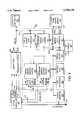
- FIG. 3is a block diagram of a unified memory architecture (UMA) computer system 300 in accordance with one embodiment of the present invention.
- UMA systemincludes CPU 301, system controller 302, data path controller 303, unified DRAM memory array 304, graphics controller 305, expansion frame buffer memory 306 and CRT display 307. Buses 311-319 connect the various elements of UMA system 300.
- CPU address bus 316 and CPU data bus 317connect CPU 301 to system controller 302 and data path controller 303, respectively.
- Data/control bus 315connects system controller 302 to data path controller 303.
- Address/control bus 312connects system controller 302, graphics controller 305 and unified memory 304.
- Handshake control signal bus 313connects system controller 302 to graphics controller 305.
- Unified memory data bus 314connects unified memory 304, data path controller 303 and graphics controller 305.
- Address/data bus 318connects graphics controller 305 to expansion frame buffer memory 306.
- Display bus 319connects graphics controller 305 to CRT display 307.
- system (PCI) bus 311connects system controller 302 and graphics controller 305. The signals transmitted on buses 311-319 are discussed in more detail below.
- Unified memory 304which is conventionally implemented using a DRAM array, is logically partitioned into main memory array 304a and main frame buffer memory 304b.
- Main frame buffer memory 304bforms a first portion of a complete frame buffer memory.
- Expansion frame buffer memory 306forms the second portion of the complete frame buffer memory.
- Frame buffer memory 304b and expansion frame buffer memory 306are physically separate memories.
- Frame buffer memory 304b and expansion frame buffer memory 306are accessed on independent buses and are accessed using separate address/control circuitry within graphics controller 305.
- expansion frame buffer memory 306has a capacity equal to one half of the total frame buffer capacity required by the high resolution display mode of the computer system. For example, if the high resolution display mode of UMA system 300 requires a 4 MByte frame buffer, expansion frame buffer memory 306 is selected to have a capacity of 2 MBytes and main frame buffer memory 304b is selected to have a capacity of 2 MBytes. In other embodiments, the complete frame buffer memory is allocated between expansion frame buffer memory 306 and main frame buffer memory 304b using other proportions.
- the capacity of unified memory 304is selected such that main memory 304a has the desired capacity in view of the capacity required for main frame buffer memory 304b.
- unified memory 304must have a total capacity of 16 Mbytes to provide a main memory 304 having a capacity of 14 Mbytes and a main frame buffer memory 304b having a capacity of 2 Mbytes.
- expansion frame buffer memory 306has at least the same data bandwidth as unified memory 304, although this is not required.
- unified memory 304has a data bandwidth of 528 MBytes/sec.
- unified memory 304is an SDRAM (synchronous DRAM) or a burst EDO DRAM having a 64-bit wide data path (8 bytes of 8-bits each) and operating at a frequency of 66 MHz.
- expansion frame buffer memory 306is the same type of memory as unified memory 304. However, expansion frame buffer memory 306 and unified memory 304 can also be implemented using different types of memory. Because expansion frame buffer memory 306 has a relatively small capacity (i.e., 2 MBytes or less), the loading and parasitics on the expansion memory bus 318 are much less than the loading and parasitics on the unified memory data bus 314. Thus, expansion frame buffer memory 306 can be selected to operate at a higher frequency (i.e. 132 or 264 MHz) than unified memory 304, while having a narrower data bus than unified memory 304. Expansion frame buffer memory 306 can utilize multiplexed address and data signals in the manner of MDRAM (Multibank DRAM).
- MDRAMMultibank DRAM
- expansion frame buffer memory 306is a DRAM array which implements the multibank architecture as described in commonly owned, U.S. patent application Ser. No. 08/270,856, entitled “Directional Asymmetric Swing Bus System for Circuit Module Architecture", by Leung et al., now U.S. Pat. No. 5,655,133 issued Aug. 5, 1997, which is hereby incorporated by reference in its entirety.
- expansion frame buffer memory 306has a data bus with a width of 16-bits (2 bytes) and is operated at a frequency of 132 MHz (operated at both edges of the clock signal for a data bandwidth of 528 MBytes/sec).
- expansion frame buffer memory 306requires only 26 pins to interface with graphics controller 305.
- Multibank architectureis further described in Przybylski, "MoSys Reveals MDRAM Architecture", Microprocessor Report, Dec. 25, 1995, pp. 17-20, which is hereby incorporated by reference.
- the display refresh data bandwidthis divided between unified memory 304 and expansion frame buffer memory 306.
- one half of the display refresh data bandwidthis provided by expansion frame buffer memory 306, and the other half of the display refresh data bandwidth is provided by unified memory 304.
- a substantial amount of the data bandwidth of unified memory 304is made available to CPU 301 and other system elements, thereby improving the performance of UMA system 300.
- FIG. 4is a block diagram which illustrates graphics controller 305 in more detail in accordance with one embodiment of the invention.
- Graphics controller 305includes display controller 401, graphics accelerator 402, video processor 403, system interface 404, unified memory address/control circuit 410, unified memory data interface 411, expansion memory address/control circuit 420, expansion memory data buffer 421 and expansion memory data interface 422.
- Processors 401-404, unified memory address/control circuit 410 and unified memory data interface circuit 411are elements found in conventional UMA systems.
- Unified memory data interface 411 and expansion memory data interface 422are connected to display controller 401 by a dedicated bus 416. Unified memory data interface 411 and expansion memory data interface are also connected to processors 402-404 by another dedicated bus 415.
- Display controller 401has control lines which are coupled to bus 415, and optionally has data lines which are connected to bus 415. Buses 415 and 416 provide display controller 401 and processors 402-404 with a maximum data bandwidth equal to the total combined bandwidth of buses 415 and 416. As a result, the total data bandwidth available to display controller 401 and processors 402-404 is increased without requiring a wider internal data bus. A wider internal data bus would consume significantly more silicon area than buses 415 and 416.
- the interface signals used by graphics controller 305, system controller 302 and unified memory 304are similar to the interface signals used in a conventional UMA system.
- FIG. 5illustrates the interface signals in accordance with one embodiment of the invention. These interface signals include: multiplexed row and column address signals MA 11:0! for addressing unified memory 304; column address strobe signals CAS# 7:0! for latching in the column address, advancing the column address (in burst-type DRAM memory), and byte write masking for a single write operation; row address strobe signals RAS# 1:0! for latching in the row address and selecting a memory bank within unified memory 304; and a write enable signal WE# for indicating whether the access is read or write operation.
- the MA 11:0!, CAS# 7:0!, RAS# 1:0! and WE# signalsare generated by system controller 202 or unified memory address/control circuit 410 and provided to unified memory 304 on bus 312 (FIG. 4).
- the interface signalsalso include a memory request signal MREQ# generated by unified memory address/control circuit 410 to request access to unified memory 304; a memory request 410 priority signal MPR generated by unified memory address/control circuit 410 to indicate whether the memory request has a high or low priority; and a memory grant signal MGNT# generated by system controller 302 to indicate that system controller 302 has granted graphics controller 305 access to unified memory 304.
- a memory request signal MREQ#generated by unified memory address/control circuit 410 to request access to unified memory 304
- MPRgenerated by unified memory address/control circuit 410 to indicate whether the memory request has a high or low priority
- MGNT#generated by system controller 302 to indicate that system controller 302 has granted graphics controller 305 access to unified memory 304.
- UMA system 300additionally includes a special row access signal RASEX# which is generated by system controller 302 and provided to expansion memory address/control circuit 420 to enable graphics controller 305 to access expansion frame buffer memory 306.
- RASEX#which is generated by system controller 302 and provided to expansion memory address/control circuit 420 to enable graphics controller 305 to access expansion frame buffer memory 306.
- the previously described interface signalsare used to control the following operations within UMA system 300: (1) CPU 301 write to unified memory 304, (2) CPU 301 write to expansion frame buffer memory 306, (3) graphics controller 305 read from unified memory 304, (4) graphics controller 305 read from expansion frame buffer memory 306, (5) CPU 301 read from unified memory 304, and (6) CPU 301 read from expansion frame buffer memory 306. Each of these operations is described in more detail below.
- CPU 301To perform a write operation to unified memory 304, CPU 301 provides the appropriate address and control signals to system controller 302 on CPU address bus 316, and the appropriate data value (or values) to data path controller 303 on CPU data bus 317.
- system controller 302provides multiplexed address signals MA 11:0!, column access signals CAS# 7:0!, row access signals RAS# 1:0! and write enable signal WE# to unified memory 304 on bus 312.
- the data valueis provided by data path controller 303 to unified memory 304 on data bus 314.
- the data valueis written to the appropriate address within unified memory 304.
- system controller 302does not activate the RASEX# signal.
- graphics controller 305does not access expansion frame buffer memory 306.
- CPU 301When CPU 301 is to perform a write access to expansion frame buffer memory 306, CPU 301 instructs system controller 302 to de-activate all row access signals RAS 1:0!# and to activate the RASEX# signal. Because the row access signals RAS# 1:0! are not activated, unified memory 304 is not enabled. The RASEX# signal enables expansion memory address/control circuit 420. In response to instructions received from CPU 301, system controller 302 generates multiplexed address signals MA 11:0!, column access signals CAS# 7:0!, and a write enable signal WE# which are used to address expansion frame buffer memory 306.
- FIG. 6is a waveform diagram illustrating the interface signals when CPU 301 performs a write operation to expansion frame buffer memory 306.
- Expansion memory address/control circuit 420latches in a row address from the multiplexed address signals MA 11:0! at the falling edge of the RASEX# signal.
- Expansion memory address/control circuit 420latches in a column address from the multiplexed address signals MA 11:0! at the falling edge of any one of the column access signals CAS# 7:0!.
- Expansion memory address/control circuit 420transmits control signals to enable expansion memory data buffer 421.
- the data value to be writtenis provided by CPU 301, through data path controller 303, to data bus 314.
- This data valueis latched in the expansion memory data buffer 421 at minimum latency and maximum bandwidth when the expansion memory data buffer 421 is enabled.
- each successive falling edge of the column access signals CAS# 7:0!will latch a new data value on data bus 314 into expansion memory data buffer 421.
- Expansion memory address/control circuit 420transmits the received row and column address signals to expansion memory data interface 422 on bus 415. In one embodiment, these signals are the same as the signals received by expansion memory address/control circuit 420. In another embodiment, these address signals are modified to allow the use of an expansion frame buffer memory 306 which has a different addressing scheme than unified memory 304. Expansion memory data interface 422 then retrieves the data value (or data values) from expansion memory data buffer 421.
- Expansion memory data interface 422transmits the received address signals and data value(s) to expansion frame buffer memory 306 on bus 318, thereby causing the data value(s) to be written to the appropriate address(es) within expansion frame buffer memory 306.
- Expansion memory data interface circuit 422does not retrieve the data values stored in expansion memory data buffer 421 until expansion frame buffer memory 306 is available. Expansion memory data interface 422 manages this operation.
- expansion memory address/control circuit 420asserts the memory request signal MREQ# along with a low memory priority signal MPR when CPU 301 is performing a write access to expansion frame buffer memory 306.
- CPU 301will not attempt another write operation to expansion frame buffer memory 306 until after the memory request signal MREQ# is de-asserted.
- the memory request signal MREQ#is not de-asserted until after the data values stored in expansion memory data buffer 421 are successfully written to expansion frame buffer memory 306.
- Expansion memory data interface 422manages this operation. As a result, CPU 301 is prevented from overwriting data values stored in expansion memory data buffer 421.
- Graphics controller 305performs the display refresh operation by accessing unified memory 304 and expansion frame buffer memory 306.
- display controller 401transmits the appropriate address and control signals to unified memory address/control circuit 410.
- unified memory address/control circuit 410asserts the memory request signal MREQ# and the memory priority signal MPR, which are provided to system controller 302.
- the display refresh operationis given a high priority. Consequently, system controller 302 will not perform any additional write operations to unified memory 304 or expansion frame buffer memory 306 until the display refresh request has been granted.
- System controller 302asserts the memory access granted signal MGNT# to unified memory address/control circuit 410 to indicate that access to unified memory 304 has been granted.
- unified memory address/control circuit 410transmits multiplexed address signals MA 11:0!, column access signals CAS# 7:0!, row access signals RAS# 1:0!, and write enable signal WE# to unified memory 304 on bus 312.
- unified memory 304provides the requested data value(s) on data bus 314.
- Unified memory address/control circuit 410then transmits a signal to unified memory data interface 411 on bus 415 to cause the data value(s) to be routed from bus 314, through unified memory data interface 411 to display controller 401.
- Display controller 401then transmits the receive data value(s) to CRT display 307 for display.
- expansion memory data interface 422To read display data from expansion frame buffer memory 306, display controller 401 transmits the appropriate address and control signals to expansion memory data interface 422. In response, expansion memory data interface 422 provides the appropriate address and control signals to expansion frame buffer memory 306 on bus 415, thereby causing the desired data value(s) to be read from expansion frame buffer memory 306 on bus 318. Expansion memory data interface 422 routes the data value(s) to display controller 401 on bus 416, which in turn provides the data value(s) to CRT display 307 on bus 319. Expansion memory data interface 422 prevents system controller 302 from accessing expansion frame buffer memory 306 at this time.
- CPU 301can read data from unified memory 304 by transmitting the appropriate address signals to system controller 302 on CPU address bus 316.
- System controller 302then generates the appropriate signals (i.e., MA 11:0!, CAS# 7:0!, RAS# 1:0! and WE# (deasserted)) and transmits these signals to unified memory 304.
- the requested data value(s)are read from unified memory 304 to data bus 314.
- Data path controller 303then routes the data value(s) from bus 314 to CPU 301 on CPU data bus 317.
- CPU 301can read data from expansion frame buffer memory 306 in one of two ways.
- CPU 301transmits the appropriate address and control signals to system controller 302 on CPU address bus 316.
- System controller 302transmits these signals to system interface 404 on system bus 311.
- System interface 404then transmits the appropriate read signals to expansion data memory interface 422 on bus 415.
- the appropriate data valuesare read from expansion frame buffer memory 306 to CPU 301 through expansion memory data interface 422, bus 415, system interface 404, system bus 311, system controller 302, data/control bus 315, data path controller 303 and CPU data bus 317.
- a second method for reading data from expansion frame buffer memory 306 by CPU 301is performed as follows. Expansion frame buffer memory 306 is accessed through system controller 302, expansion memory address/control circuit 420 and expansion memory data interface 422 in a manner which is substantially similar to the manner in which CPU 301 performs a write access to expansion frame buffer memory 306. However, in the present method, the write enable signal WE# is not asserted. As a result, the desired data value is read from expansion frame buffer memory 306 to expansion memory data interface 422. This data value is then transmitted from expansion memory data interface 422 to expansion memory data buffer 421. Expansion memory data buffer 421 provides the data value to data path controller 303 on bus 314. Data path controller 303 then provides the data value to CPU 301 on CPU data bus 317. This method of accessing expansion frame buffer memory 306 does not require the use of system bus 311. As a result, this method of accessing expansion frame buffer memory 306 is faster than the first method described above.
- FIG. 7ais a waveform diagram illustrating a method of performing a display refresh operation in accordance with one embodiment of the present invention.
- graphics controller 305reads data values from both main frame buffer memory 304b and expansion frame buffer memory 306.
- graphics controller 305alternately accesses frame buffer memory 304b and expansion frame buffer memory 306 such that interleaved display data bursts are provided to display controller 401.
- display controller 401loads data with maximum efficiency while allowing CPU 301 and the other graphics processors 402-404 to access the unified memory 304 and the expansion frame buffer memory 306 with maximum available data bandwidth and minimum circuit overhead.
- FIG. 7billustrates display address mapping which allows the display refresh data to be interleaved.
- the lower 4 bits C 3:0! of the column addresscorrespond to the data burst size. In the example illustrated, 16 words of 8 bytes each are combined to form a 128 byte burst.
- An expansion bit, Eis inserted between the upper 4 bits C 8:4! of the column address and the lower 4 bits C 3:0! of the column address.
- the row address signals R 8:0!are added after the upper four bits C 8:4! of the column address.
- the R 8:0! and C 8:4! bitsmay or may not be scrambled to optimize the performance of the graphics system.
- expansion frame buffer memory 306is higher than the data bandwidth of unified memory 304, it is advantageous to configure all or most of the display frame buffer memory (which requires high data bandwidth for the display refresh operation) inside the expansion frame buffer memory 306. All other video memory (required for video windows, offscreen scratch pads or caching areas) are then maintained inside main frame buffer memory 304b within unified memory 304 to enable higher system performance.
Landscapes
- Engineering & Computer Science (AREA)
- Computer Hardware Design (AREA)
- Theoretical Computer Science (AREA)
- Physics & Mathematics (AREA)
- General Physics & Mathematics (AREA)
- Computer Graphics (AREA)
- Software Systems (AREA)
- General Engineering & Computer Science (AREA)
- Controls And Circuits For Display Device (AREA)
- Dram (AREA)
Abstract
Description
Claims (11)
Priority Applications (3)
| Application Number | Priority Date | Filing Date | Title |
|---|---|---|---|
| US08/587,379US5790138A (en) | 1996-01-16 | 1996-01-16 | Method and structure for improving display data bandwidth in a unified memory architecture system |
| AU15238/97AAU1523897A (en) | 1996-01-16 | 1997-01-15 | Method and structure for improving display data bandwidth in a unified memory architecture system |
| PCT/US1997/000014WO1997026604A1 (en) | 1996-01-16 | 1997-01-15 | Method and structure for improving display data bandwidth in a unified memory architecture system |
Applications Claiming Priority (1)
| Application Number | Priority Date | Filing Date | Title |
|---|---|---|---|
| US08/587,379US5790138A (en) | 1996-01-16 | 1996-01-16 | Method and structure for improving display data bandwidth in a unified memory architecture system |
Publications (1)
| Publication Number | Publication Date |
|---|---|
| US5790138Atrue US5790138A (en) | 1998-08-04 |
Family
ID=24349564
Family Applications (1)
| Application Number | Title | Priority Date | Filing Date |
|---|---|---|---|
| US08/587,379Expired - LifetimeUS5790138A (en) | 1996-01-16 | 1996-01-16 | Method and structure for improving display data bandwidth in a unified memory architecture system |
Country Status (3)
| Country | Link |
|---|---|
| US (1) | US5790138A (en) |
| AU (1) | AU1523897A (en) |
| WO (1) | WO1997026604A1 (en) |
Cited By (26)
| Publication number | Priority date | Publication date | Assignee | Title |
|---|---|---|---|---|
| WO1999020010A1 (en)* | 1997-10-09 | 1999-04-22 | Interval Research Corporation | Variable bandwidth communication systems and methods |
| US6057862A (en)* | 1997-07-01 | 2000-05-02 | Memtrax Llc | Computer system having a common display memory and main memory |
| US6118462A (en)* | 1997-07-01 | 2000-09-12 | Memtrax Llc | Computer system controller having internal memory and external memory control |
| US6128026A (en)* | 1998-05-04 | 2000-10-03 | S3 Incorporated | Double buffered graphics and video accelerator having a write blocking memory interface and method of doing the same |
| US6266753B1 (en)* | 1997-07-10 | 2001-07-24 | Cirrus Logic, Inc. | Memory manager for multi-media apparatus and method therefor |
| US6333745B1 (en)* | 1996-09-30 | 2001-12-25 | Hitachi, Ltd. | Data processor having unified memory architecture providing priority memory access |
| US6351271B1 (en) | 1997-10-09 | 2002-02-26 | Interval Research Corporation | Method and apparatus for sending and receiving lightweight messages |
| US20020063716A1 (en)* | 2000-11-30 | 2002-05-30 | Palm, Inc. | Control of color depth in a computing device |
| US20030030004A1 (en)* | 2001-01-31 | 2003-02-13 | General Electric Company | Shared memory control between detector framing node and processor |
| US6754546B1 (en) | 1997-10-09 | 2004-06-22 | Interval Research Corporation | Electronic audio connection system and methods for providing same |
| US20040183806A1 (en)* | 2003-03-20 | 2004-09-23 | International Business Machines Corporation | Method and apparatus for simulated direct frame buffer access for graphics adapters |
| US20040263521A1 (en)* | 2003-06-30 | 2004-12-30 | Booth Lawrence A | System and method for high-speed communications between an application processor and coprocessor |
| US6839063B2 (en) | 2000-08-25 | 2005-01-04 | Renesas Technology Corp. | Memory access methods in a unified memory system |
| US6853381B1 (en)* | 1999-09-16 | 2005-02-08 | Ati International Srl | Method and apparatus for a write behind raster |
| US20050212806A1 (en)* | 2002-05-10 | 2005-09-29 | Metod Koselj | Graphics engine converting individual commands to spatial image information, and electrical device and memory incorporating the graphics engine |
| US6956497B1 (en) | 1997-10-09 | 2005-10-18 | Vulcan Patents Llc | Method and apparatus for sending presence messages |
| US20050253859A1 (en)* | 2004-05-13 | 2005-11-17 | Renesas Technology Corporation | System LSI and data processing system |
| US7068847B1 (en)* | 2000-09-08 | 2006-06-27 | Sunplus Technology Co., Ltd. | High-resolution still picture decoding device |
| CN1306426C (en)* | 2005-05-30 | 2007-03-21 | 威盛电子股份有限公司 | Motherboard and its bridge modules |
| US7307667B1 (en)* | 2003-06-27 | 2007-12-11 | Zoran Corporation | Method and apparatus for an integrated high definition television controller |
| CN100357934C (en)* | 2005-05-30 | 2007-12-26 | 威盛电子股份有限公司 | Motherboard and its control method |
| US20080158117A1 (en)* | 2006-12-27 | 2008-07-03 | Palm, Inc. | Power saving display |
| US20080168250A1 (en)* | 2007-01-05 | 2008-07-10 | Samsung Electronics Co., Ltd. | Unified memory apparatus for reconfigurable processor and method of using the unified memory apparatus |
| US7545359B1 (en) | 1995-08-03 | 2009-06-09 | Vulcan Patents Llc | Computerized interactor systems and methods for providing same |
| US8064280B1 (en)* | 2008-06-10 | 2011-11-22 | Altera Corporation | Scaleable look-up table based memory |
| US20230093805A1 (en)* | 2021-09-30 | 2023-03-30 | Lenovo (Beijing) Limited | Electronic device and processing method |
Families Citing this family (9)
| Publication number | Priority date | Publication date | Assignee | Title |
|---|---|---|---|---|
| EP1039892B1 (en) | 1997-02-21 | 2004-04-28 | Abbott Laboratories | Use of polyunsaturated fatty acids for reducing the incidence of necrotizing enterocolitis |
| US5941968A (en)* | 1997-04-14 | 1999-08-24 | Advanced Micro Devices, Inc. | Computer system for concurrent data transferring between graphic controller and unified system memory and between CPU and expansion bus device |
| US6076180A (en) | 1997-06-23 | 2000-06-13 | Micron Electronics, Inc. | Method for testing a controller with random constraints |
| WO1999028893A1 (en)* | 1997-12-01 | 1999-06-10 | Mediaq, Inc. | High performance, highly integrated computer architecture with extendible embedded memory |
| WO1999034294A1 (en)* | 1997-12-24 | 1999-07-08 | Creative Technology Ltd. | Optimal multi-channel memory controller system |
| JP4022369B2 (en)* | 1997-12-30 | 2007-12-19 | マイクロン テクノロジー,インコーポレイテッド | Accelerated graphics port for multi-memory controller computer system |
| US6252612B1 (en) | 1997-12-30 | 2001-06-26 | Micron Electronics, Inc. | Accelerated graphics port for multiple memory controller computer system |
| US7071946B2 (en) | 1997-12-30 | 2006-07-04 | Micron Technology, Inc. | Accelerated graphics port for a multiple memory controller computer system |
| US6157398A (en) | 1997-12-30 | 2000-12-05 | Micron Technology, Inc. | Method of implementing an accelerated graphics port for a multiple memory controller computer system |
Citations (4)
| Publication number | Priority date | Publication date | Assignee | Title |
|---|---|---|---|---|
| US5335322A (en)* | 1992-03-31 | 1994-08-02 | Vlsi Technology, Inc. | Computer display system using system memory in place or dedicated display memory and method therefor |
| US5450542A (en)* | 1993-11-30 | 1995-09-12 | Vlsi Technology, Inc. | Bus interface with graphics and system paths for an integrated memory system |
| US5572655A (en)* | 1993-01-12 | 1996-11-05 | Lsi Logic Corporation | High-performance integrated bit-mapped graphics controller |
| US5608427A (en)* | 1993-12-09 | 1997-03-04 | Sun Microsystems, Inc. | Interleaving pixel data for a memory display interface |
- 1996
- 1996-01-16USUS08/587,379patent/US5790138A/ennot_activeExpired - Lifetime
- 1997
- 1997-01-15WOPCT/US1997/000014patent/WO1997026604A1/enactiveApplication Filing
- 1997-01-15AUAU15238/97Apatent/AU1523897A/ennot_activeAbandoned
Patent Citations (4)
| Publication number | Priority date | Publication date | Assignee | Title |
|---|---|---|---|---|
| US5335322A (en)* | 1992-03-31 | 1994-08-02 | Vlsi Technology, Inc. | Computer display system using system memory in place or dedicated display memory and method therefor |
| US5572655A (en)* | 1993-01-12 | 1996-11-05 | Lsi Logic Corporation | High-performance integrated bit-mapped graphics controller |
| US5450542A (en)* | 1993-11-30 | 1995-09-12 | Vlsi Technology, Inc. | Bus interface with graphics and system paths for an integrated memory system |
| US5608427A (en)* | 1993-12-09 | 1997-03-04 | Sun Microsystems, Inc. | Interleaving pixel data for a memory display interface |
Non-Patent Citations (2)
| Title |
|---|
| Przybylski, Steven, Microprocessor Report, MoSys Reveals MDRAM Architecture, Radical Alternative Is Not Just Another VRAM , Dec. 25, 1995, pp. 17 20.* |
| Przybylski, Steven, Microprocessor Report, MoSys Reveals MDRAM Architecture, Radical Alternative Is Not Just Another VRAM, Dec. 25, 1995, pp. 17-20. |
Cited By (52)
| Publication number | Priority date | Publication date | Assignee | Title |
|---|---|---|---|---|
| US8154511B2 (en) | 1995-08-03 | 2012-04-10 | Vintell Applications Ny, Llc | Computerized interactor systems and methods for providing same |
| US7545359B1 (en) | 1995-08-03 | 2009-06-09 | Vulcan Patents Llc | Computerized interactor systems and methods for providing same |
| US6333745B1 (en)* | 1996-09-30 | 2001-12-25 | Hitachi, Ltd. | Data processor having unified memory architecture providing priority memory access |
| US6954206B2 (en) | 1996-09-30 | 2005-10-11 | Hitachi, Ltd. | Data processor having unified memory architecture using register to optimize memory access |
| US7333116B2 (en) | 1996-09-30 | 2008-02-19 | Renesas Technology Corporation | Data processor having unified memory architecture using register to optimize memory access |
| US20050264574A1 (en)* | 1996-09-30 | 2005-12-01 | Tetsuya Shimomura | Data processor having unified memory architecture using register to optimize memory access |
| US20040056865A1 (en)* | 1996-09-30 | 2004-03-25 | Tetsuya Shimomura | Data processor having unified memory architecture using register to optimize memory access |
| US6717583B2 (en) | 1996-09-30 | 2004-04-06 | Hitachi, Ltd. | Data processor having unified memory architecture providing priority memory access |
| US6118462A (en)* | 1997-07-01 | 2000-09-12 | Memtrax Llc | Computer system controller having internal memory and external memory control |
| USRE41413E1 (en) | 1997-07-01 | 2010-07-06 | Neal Margulis | Computer system controller having internal memory and external memory control |
| US6057862A (en)* | 1997-07-01 | 2000-05-02 | Memtrax Llc | Computer system having a common display memory and main memory |
| US6690379B2 (en) | 1997-07-01 | 2004-02-10 | Memtrax Llc | Computer system controller having internal memory and external memory control |
| US6266753B1 (en)* | 1997-07-10 | 2001-07-24 | Cirrus Logic, Inc. | Memory manager for multi-media apparatus and method therefor |
| US7953112B2 (en) | 1997-10-09 | 2011-05-31 | Interval Licensing Llc | Variable bandwidth communication systems and methods |
| US6351271B1 (en) | 1997-10-09 | 2002-02-26 | Interval Research Corporation | Method and apparatus for sending and receiving lightweight messages |
| WO1999020010A1 (en)* | 1997-10-09 | 1999-04-22 | Interval Research Corporation | Variable bandwidth communication systems and methods |
| US6282206B1 (en)* | 1997-10-09 | 2001-08-28 | Interval Research Corporation | Variable bandwidth communication systems and methods |
| US20070280290A1 (en)* | 1997-10-09 | 2007-12-06 | Debby Hindus | Variable bandwidth communication systems and methods |
| US8416806B2 (en) | 1997-10-09 | 2013-04-09 | Interval Licensing Llc | Variable bandwidth communication systems and methods |
| US8509137B2 (en) | 1997-10-09 | 2013-08-13 | Interval Licensing Llc | Method and apparatus for sending presence messages |
| US20110228039A1 (en)* | 1997-10-09 | 2011-09-22 | Debby Hindus | Variable bandwidth communication systems and methods |
| US6754546B1 (en) | 1997-10-09 | 2004-06-22 | Interval Research Corporation | Electronic audio connection system and methods for providing same |
| US6956497B1 (en) | 1997-10-09 | 2005-10-18 | Vulcan Patents Llc | Method and apparatus for sending presence messages |
| US6128026A (en)* | 1998-05-04 | 2000-10-03 | S3 Incorporated | Double buffered graphics and video accelerator having a write blocking memory interface and method of doing the same |
| US6853381B1 (en)* | 1999-09-16 | 2005-02-08 | Ati International Srl | Method and apparatus for a write behind raster |
| US7557809B2 (en) | 2000-08-25 | 2009-07-07 | Renesas Technology Corp. | Memory access methods in a unified memory system |
| US20050062749A1 (en)* | 2000-08-25 | 2005-03-24 | Yasuhiro Nakatsuka | Memory access methods in a unified memory system |
| US6839063B2 (en) | 2000-08-25 | 2005-01-04 | Renesas Technology Corp. | Memory access methods in a unified memory system |
| US7068847B1 (en)* | 2000-09-08 | 2006-06-27 | Sunplus Technology Co., Ltd. | High-resolution still picture decoding device |
| US20020063716A1 (en)* | 2000-11-30 | 2002-05-30 | Palm, Inc. | Control of color depth in a computing device |
| US20080062182A1 (en)* | 2000-11-30 | 2008-03-13 | Palm, Inc. | Control of color depth in a computing device |
| US20030030004A1 (en)* | 2001-01-31 | 2003-02-13 | General Electric Company | Shared memory control between detector framing node and processor |
| US6753873B2 (en)* | 2001-01-31 | 2004-06-22 | General Electric Company | Shared memory control between detector framing node and processor |
| US20050212806A1 (en)* | 2002-05-10 | 2005-09-29 | Metod Koselj | Graphics engine converting individual commands to spatial image information, and electrical device and memory incorporating the graphics engine |
| US20060033745A1 (en)* | 2002-05-10 | 2006-02-16 | Metod Koselj | Graphics engine with edge draw unit, and electrical device and memopry incorporating the graphics engine |
| US7248267B2 (en)* | 2003-03-20 | 2007-07-24 | International Business Machines Corporation | Method and apparatus for simulated direct frame buffer access for graphics adapters |
| US20040183806A1 (en)* | 2003-03-20 | 2004-09-23 | International Business Machines Corporation | Method and apparatus for simulated direct frame buffer access for graphics adapters |
| US7307667B1 (en)* | 2003-06-27 | 2007-12-11 | Zoran Corporation | Method and apparatus for an integrated high definition television controller |
| US7038687B2 (en)* | 2003-06-30 | 2006-05-02 | Intel Corporation | System and method for high-speed communications between an application processor and coprocessor |
| US20040263521A1 (en)* | 2003-06-30 | 2004-12-30 | Booth Lawrence A | System and method for high-speed communications between an application processor and coprocessor |
| US20050253859A1 (en)* | 2004-05-13 | 2005-11-17 | Renesas Technology Corporation | System LSI and data processing system |
| CN100357934C (en)* | 2005-05-30 | 2007-12-26 | 威盛电子股份有限公司 | Motherboard and its control method |
| CN1306426C (en)* | 2005-05-30 | 2007-03-21 | 威盛电子股份有限公司 | Motherboard and its bridge modules |
| US7995050B2 (en) | 2006-12-27 | 2011-08-09 | Hewlett-Packard Development Company, L.P. | Power saving display |
| US20080158117A1 (en)* | 2006-12-27 | 2008-07-03 | Palm, Inc. | Power saving display |
| US20080168250A1 (en)* | 2007-01-05 | 2008-07-10 | Samsung Electronics Co., Ltd. | Unified memory apparatus for reconfigurable processor and method of using the unified memory apparatus |
| US8064280B1 (en)* | 2008-06-10 | 2011-11-22 | Altera Corporation | Scaleable look-up table based memory |
| US8644100B2 (en) | 2008-06-10 | 2014-02-04 | Altera Corporation | Scaleable look-up table based memory |
| US9123437B1 (en) | 2008-06-10 | 2015-09-01 | Altera Corporation | Scaleable look-up table based memory |
| US9548103B1 (en) | 2008-06-10 | 2017-01-17 | Altera Corporation | Scaleable look-up table based memory |
| US20230093805A1 (en)* | 2021-09-30 | 2023-03-30 | Lenovo (Beijing) Limited | Electronic device and processing method |
| US11940948B2 (en)* | 2021-09-30 | 2024-03-26 | Lenovo (Beijing) Limited | Electronic device having multiple processing units and multiple memory units, and processing method thereof |
Also Published As
| Publication number | Publication date |
|---|---|
| AU1523897A (en) | 1997-08-11 |
| WO1997026604A1 (en) | 1997-07-24 |
Similar Documents
| Publication | Publication Date | Title |
|---|---|---|
| US5790138A (en) | Method and structure for improving display data bandwidth in a unified memory architecture system | |
| US6215497B1 (en) | Method and apparatus for maximizing the random access bandwidth of a multi-bank DRAM in a computer graphics system | |
| US7543101B2 (en) | System of accessing data in a graphics system and method thereof | |
| US5617118A (en) | Mode dependent minimum FIFO fill level controls processor access to video memory | |
| US5353402A (en) | Computer graphics display system having combined bus and priority reading of video memory | |
| US6327642B1 (en) | Parallel access virtual channel memory system | |
| US5572655A (en) | High-performance integrated bit-mapped graphics controller | |
| US5129059A (en) | Graphics processor with staggered memory timing | |
| US8954687B2 (en) | Memory hub and access method having a sequencer and internal row caching | |
| JP2909592B2 (en) | Computer memory system | |
| US6195106B1 (en) | Graphics system with multiported pixel buffers for accelerated pixel processing | |
| KR100329893B1 (en) | High bandwidth dram with low operating power modes | |
| US5454076A (en) | Method and apparatus for simultaneously minimizing storage and maximizing total memory bandwidth for a repeating pattern | |
| JP2002526882A (en) | Read / write buffer which is completely unaffected by refresh of semiconductor memory and method of operating the same | |
| JPH0934783A (en) | Semiconductor memory device | |
| US6108015A (en) | Circuits, systems and methods for interfacing processing circuitry with a memory | |
| JPH0313796Y2 (en) | ||
| US5793663A (en) | Multiple page memory | |
| JP2002366431A (en) | Apparatus for accessing embedded memory of application specific integrated circuits | |
| JPH11510620A (en) | Integrated system / frame buffer memory and system, and methods of using them | |
| US6809737B1 (en) | Method and apparatus for supporting multiple monitor orientations | |
| US6433786B1 (en) | Memory architecture for video graphics environment | |
| US5642136A (en) | Method and apparatus for screen refresh bandwidth reduction for video display modes | |
| EP0801375A2 (en) | A memory with optimized memory space and wide data input/output and systems and methods using the same | |
| US6072745A (en) | Method for operating a memory |
Legal Events
| Date | Code | Title | Description |
|---|---|---|---|
| AS | Assignment | Owner name:MONOLITHIC SYSTEM TECHNOLOGY, INC., CALIFORNIA Free format text:ASSIGNMENT OF ASSIGNORS INTEREST;ASSIGNOR:HSU, FU-CHIEH;REEL/FRAME:007875/0353 Effective date:19960116 | |
| STCF | Information on status: patent grant | Free format text:PATENTED CASE | |
| FEPP | Fee payment procedure | Free format text:PAT HOLDER NO LONGER CLAIMS SMALL ENTITY STATUS, ENTITY STATUS SET TO UNDISCOUNTED (ORIGINAL EVENT CODE: STOL); ENTITY STATUS OF PATENT OWNER: LARGE ENTITY | |
| FPAY | Fee payment | Year of fee payment:4 | |
| FPAY | Fee payment | Year of fee payment:8 | |
| AS | Assignment | Owner name:MOSYS, INC., CALIFORNIA Free format text:CHANGE OF NAME;ASSIGNOR:MONOLITHIC SYSTEM TECHNOLOGY, INC.;REEL/FRAME:020741/0975 Effective date:20060525 Owner name:MOSYS, INC.,CALIFORNIA Free format text:CHANGE OF NAME;ASSIGNOR:MONOLITHIC SYSTEM TECHNOLOGY, INC.;REEL/FRAME:020741/0975 Effective date:20060525 | |
| FPAY | Fee payment | Year of fee payment:12 | |
| AS | Assignment | Owner name:INGALLS & SNYDER LLC, NEW YORK Free format text:SECURITY INTEREST;ASSIGNOR:MOSYS, INC.;REEL/FRAME:038081/0262 Effective date:20160314 | |
| AS | Assignment | Owner name:INGALLS & SNYDER LLC, NEW YORK Free format text:RELEASE BY SECURED PARTY;ASSIGNOR:PERASO INC. F/K/A MOSYS, INC.;REEL/FRAME:061593/0094 Effective date:20221003 |