US5789813A - Ball grid array package with inexpensive threaded secure locking mechanism to allow removal of a threaded heat sink therefrom - Google Patents
Ball grid array package with inexpensive threaded secure locking mechanism to allow removal of a threaded heat sink therefromDownload PDFInfo
- Publication number
- US5789813A US5789813AUS08/724,076US72407696AUS5789813AUS 5789813 AUS5789813 AUS 5789813AUS 72407696 AUS72407696 AUS 72407696AUS 5789813 AUS5789813 AUS 5789813A
- Authority
- US
- United States
- Prior art keywords
- package
- substrate
- lock ring
- encapsulant
- die
- Prior art date
- Legal status (The legal status is an assumption and is not a legal conclusion. Google has not performed a legal analysis and makes no representation as to the accuracy of the status listed.)
- Expired - Lifetime
Links
Images


Classifications
- H—ELECTRICITY
- H01—ELECTRIC ELEMENTS
- H01L—SEMICONDUCTOR DEVICES NOT COVERED BY CLASS H10
- H01L23/00—Details of semiconductor or other solid state devices
- H01L23/34—Arrangements for cooling, heating, ventilating or temperature compensation ; Temperature sensing arrangements
- H01L23/42—Fillings or auxiliary members in containers or encapsulations selected or arranged to facilitate heating or cooling
- H01L23/433—Auxiliary members in containers characterised by their shape, e.g. pistons
- H01L23/4334—Auxiliary members in encapsulations
- H—ELECTRICITY
- H01—ELECTRIC ELEMENTS
- H01L—SEMICONDUCTOR DEVICES NOT COVERED BY CLASS H10
- H01L23/00—Details of semiconductor or other solid state devices
- H01L23/16—Fillings or auxiliary members in containers or encapsulations, e.g. centering rings
- H01L23/18—Fillings characterised by the material, its physical or chemical properties, or its arrangement within the complete device
- H01L23/24—Fillings characterised by the material, its physical or chemical properties, or its arrangement within the complete device solid or gel at the normal operating temperature of the device
- H—ELECTRICITY
- H01—ELECTRIC ELEMENTS
- H01L—SEMICONDUCTOR DEVICES NOT COVERED BY CLASS H10
- H01L23/00—Details of semiconductor or other solid state devices
- H01L23/34—Arrangements for cooling, heating, ventilating or temperature compensation ; Temperature sensing arrangements
- H01L23/40—Mountings or securing means for detachable cooling or heating arrangements ; fixed by friction, plugs or springs
- H01L23/4006—Mountings or securing means for detachable cooling or heating arrangements ; fixed by friction, plugs or springs with bolts or screws
- H—ELECTRICITY
- H01—ELECTRIC ELEMENTS
- H01L—SEMICONDUCTOR DEVICES NOT COVERED BY CLASS H10
- H01L23/00—Details of semiconductor or other solid state devices
- H01L23/34—Arrangements for cooling, heating, ventilating or temperature compensation ; Temperature sensing arrangements
- H01L23/40—Mountings or securing means for detachable cooling or heating arrangements ; fixed by friction, plugs or springs
- H01L23/4093—Snap-on arrangements, e.g. clips
- H—ELECTRICITY
- H01—ELECTRIC ELEMENTS
- H01L—SEMICONDUCTOR DEVICES NOT COVERED BY CLASS H10
- H01L23/00—Details of semiconductor or other solid state devices
- H01L23/34—Arrangements for cooling, heating, ventilating or temperature compensation ; Temperature sensing arrangements
- H01L23/40—Mountings or securing means for detachable cooling or heating arrangements ; fixed by friction, plugs or springs
- H01L23/4006—Mountings or securing means for detachable cooling or heating arrangements ; fixed by friction, plugs or springs with bolts or screws
- H01L2023/4037—Mountings or securing means for detachable cooling or heating arrangements ; fixed by friction, plugs or springs with bolts or screws characterised by thermal path or place of attachment of heatsink
- H01L2023/4043—Mountings or securing means for detachable cooling or heating arrangements ; fixed by friction, plugs or springs with bolts or screws characterised by thermal path or place of attachment of heatsink heatsink to have chip
- H—ELECTRICITY
- H01—ELECTRIC ELEMENTS
- H01L—SEMICONDUCTOR DEVICES NOT COVERED BY CLASS H10
- H01L23/00—Details of semiconductor or other solid state devices
- H01L23/34—Arrangements for cooling, heating, ventilating or temperature compensation ; Temperature sensing arrangements
- H01L23/40—Mountings or securing means for detachable cooling or heating arrangements ; fixed by friction, plugs or springs
- H01L23/4006—Mountings or securing means for detachable cooling or heating arrangements ; fixed by friction, plugs or springs with bolts or screws
- H01L2023/4037—Mountings or securing means for detachable cooling or heating arrangements ; fixed by friction, plugs or springs with bolts or screws characterised by thermal path or place of attachment of heatsink
- H01L2023/405—Mountings or securing means for detachable cooling or heating arrangements ; fixed by friction, plugs or springs with bolts or screws characterised by thermal path or place of attachment of heatsink heatsink to package
- H—ELECTRICITY
- H01—ELECTRIC ELEMENTS
- H01L—SEMICONDUCTOR DEVICES NOT COVERED BY CLASS H10
- H01L23/00—Details of semiconductor or other solid state devices
- H01L23/34—Arrangements for cooling, heating, ventilating or temperature compensation ; Temperature sensing arrangements
- H01L23/40—Mountings or securing means for detachable cooling or heating arrangements ; fixed by friction, plugs or springs
- H01L23/4006—Mountings or securing means for detachable cooling or heating arrangements ; fixed by friction, plugs or springs with bolts or screws
- H01L2023/4075—Mechanical elements
- H01L2023/4087—Mounting accessories, interposers, clamping or screwing parts
- H—ELECTRICITY
- H01—ELECTRIC ELEMENTS
- H01L—SEMICONDUCTOR DEVICES NOT COVERED BY CLASS H10
- H01L2224/00—Indexing scheme for arrangements for connecting or disconnecting semiconductor or solid-state bodies and methods related thereto as covered by H01L24/00
- H01L2224/01—Means for bonding being attached to, or being formed on, the surface to be connected, e.g. chip-to-package, die-attach, "first-level" interconnects; Manufacturing methods related thereto
- H01L2224/26—Layer connectors, e.g. plate connectors, solder or adhesive layers; Manufacturing methods related thereto
- H01L2224/31—Structure, shape, material or disposition of the layer connectors after the connecting process
- H01L2224/32—Structure, shape, material or disposition of the layer connectors after the connecting process of an individual layer connector
- H01L2224/321—Disposition
- H01L2224/32151—Disposition the layer connector connecting between a semiconductor or solid-state body and an item not being a semiconductor or solid-state body, e.g. chip-to-substrate, chip-to-passive
- H01L2224/32221—Disposition the layer connector connecting between a semiconductor or solid-state body and an item not being a semiconductor or solid-state body, e.g. chip-to-substrate, chip-to-passive the body and the item being stacked
- H01L2224/32225—Disposition the layer connector connecting between a semiconductor or solid-state body and an item not being a semiconductor or solid-state body, e.g. chip-to-substrate, chip-to-passive the body and the item being stacked the item being non-metallic, e.g. insulating substrate with or without metallisation
- H—ELECTRICITY
- H01—ELECTRIC ELEMENTS
- H01L—SEMICONDUCTOR DEVICES NOT COVERED BY CLASS H10
- H01L2224/00—Indexing scheme for arrangements for connecting or disconnecting semiconductor or solid-state bodies and methods related thereto as covered by H01L24/00
- H01L2224/01—Means for bonding being attached to, or being formed on, the surface to be connected, e.g. chip-to-package, die-attach, "first-level" interconnects; Manufacturing methods related thereto
- H01L2224/42—Wire connectors; Manufacturing methods related thereto
- H01L2224/47—Structure, shape, material or disposition of the wire connectors after the connecting process
- H01L2224/48—Structure, shape, material or disposition of the wire connectors after the connecting process of an individual wire connector
- H01L2224/481—Disposition
- H01L2224/48151—Connecting between a semiconductor or solid-state body and an item not being a semiconductor or solid-state body, e.g. chip-to-substrate, chip-to-passive
- H01L2224/48221—Connecting between a semiconductor or solid-state body and an item not being a semiconductor or solid-state body, e.g. chip-to-substrate, chip-to-passive the body and the item being stacked
- H01L2224/48225—Connecting between a semiconductor or solid-state body and an item not being a semiconductor or solid-state body, e.g. chip-to-substrate, chip-to-passive the body and the item being stacked the item being non-metallic, e.g. insulating substrate with or without metallisation
- H01L2224/48227—Connecting between a semiconductor or solid-state body and an item not being a semiconductor or solid-state body, e.g. chip-to-substrate, chip-to-passive the body and the item being stacked the item being non-metallic, e.g. insulating substrate with or without metallisation connecting the wire to a bond pad of the item
- H—ELECTRICITY
- H01—ELECTRIC ELEMENTS
- H01L—SEMICONDUCTOR DEVICES NOT COVERED BY CLASS H10
- H01L2224/00—Indexing scheme for arrangements for connecting or disconnecting semiconductor or solid-state bodies and methods related thereto as covered by H01L24/00
- H01L2224/01—Means for bonding being attached to, or being formed on, the surface to be connected, e.g. chip-to-package, die-attach, "first-level" interconnects; Manufacturing methods related thereto
- H01L2224/42—Wire connectors; Manufacturing methods related thereto
- H01L2224/47—Structure, shape, material or disposition of the wire connectors after the connecting process
- H01L2224/49—Structure, shape, material or disposition of the wire connectors after the connecting process of a plurality of wire connectors
- H01L2224/491—Disposition
- H01L2224/4912—Layout
- H01L2224/49175—Parallel arrangements
- H—ELECTRICITY
- H01—ELECTRIC ELEMENTS
- H01L—SEMICONDUCTOR DEVICES NOT COVERED BY CLASS H10
- H01L2224/00—Indexing scheme for arrangements for connecting or disconnecting semiconductor or solid-state bodies and methods related thereto as covered by H01L24/00
- H01L2224/73—Means for bonding being of different types provided for in two or more of groups H01L2224/10, H01L2224/18, H01L2224/26, H01L2224/34, H01L2224/42, H01L2224/50, H01L2224/63, H01L2224/71
- H01L2224/732—Location after the connecting process
- H01L2224/73251—Location after the connecting process on different surfaces
- H01L2224/73265—Layer and wire connectors
- H—ELECTRICITY
- H01—ELECTRIC ELEMENTS
- H01L—SEMICONDUCTOR DEVICES NOT COVERED BY CLASS H10
- H01L24/00—Arrangements for connecting or disconnecting semiconductor or solid-state bodies; Methods or apparatus related thereto
- H01L24/01—Means for bonding being attached to, or being formed on, the surface to be connected, e.g. chip-to-package, die-attach, "first-level" interconnects; Manufacturing methods related thereto
- H01L24/42—Wire connectors; Manufacturing methods related thereto
- H01L24/47—Structure, shape, material or disposition of the wire connectors after the connecting process
- H01L24/48—Structure, shape, material or disposition of the wire connectors after the connecting process of an individual wire connector
- H—ELECTRICITY
- H01—ELECTRIC ELEMENTS
- H01L—SEMICONDUCTOR DEVICES NOT COVERED BY CLASS H10
- H01L24/00—Arrangements for connecting or disconnecting semiconductor or solid-state bodies; Methods or apparatus related thereto
- H01L24/01—Means for bonding being attached to, or being formed on, the surface to be connected, e.g. chip-to-package, die-attach, "first-level" interconnects; Manufacturing methods related thereto
- H01L24/42—Wire connectors; Manufacturing methods related thereto
- H01L24/47—Structure, shape, material or disposition of the wire connectors after the connecting process
- H01L24/49—Structure, shape, material or disposition of the wire connectors after the connecting process of a plurality of wire connectors
- H—ELECTRICITY
- H01—ELECTRIC ELEMENTS
- H01L—SEMICONDUCTOR DEVICES NOT COVERED BY CLASS H10
- H01L24/00—Arrangements for connecting or disconnecting semiconductor or solid-state bodies; Methods or apparatus related thereto
- H01L24/73—Means for bonding being of different types provided for in two or more of groups H01L24/10, H01L24/18, H01L24/26, H01L24/34, H01L24/42, H01L24/50, H01L24/63, H01L24/71
- H—ELECTRICITY
- H01—ELECTRIC ELEMENTS
- H01L—SEMICONDUCTOR DEVICES NOT COVERED BY CLASS H10
- H01L2924/00—Indexing scheme for arrangements or methods for connecting or disconnecting semiconductor or solid-state bodies as covered by H01L24/00
- H01L2924/0001—Technical content checked by a classifier
- H01L2924/00014—Technical content checked by a classifier the subject-matter covered by the group, the symbol of which is combined with the symbol of this group, being disclosed without further technical details
- H—ELECTRICITY
- H01—ELECTRIC ELEMENTS
- H01L—SEMICONDUCTOR DEVICES NOT COVERED BY CLASS H10
- H01L2924/00—Indexing scheme for arrangements or methods for connecting or disconnecting semiconductor or solid-state bodies as covered by H01L24/00
- H01L2924/10—Details of semiconductor or other solid state devices to be connected
- H01L2924/11—Device type
- H01L2924/14—Integrated circuits
- H—ELECTRICITY
- H01—ELECTRIC ELEMENTS
- H01L—SEMICONDUCTOR DEVICES NOT COVERED BY CLASS H10
- H01L2924/00—Indexing scheme for arrangements or methods for connecting or disconnecting semiconductor or solid-state bodies as covered by H01L24/00
- H01L2924/15—Details of package parts other than the semiconductor or other solid state devices to be connected
- H01L2924/151—Die mounting substrate
- H01L2924/153—Connection portion
- H01L2924/1531—Connection portion the connection portion being formed only on the surface of the substrate opposite to the die mounting surface
- H01L2924/15311—Connection portion the connection portion being formed only on the surface of the substrate opposite to the die mounting surface being a ball array, e.g. BGA
- H—ELECTRICITY
- H01—ELECTRIC ELEMENTS
- H01L—SEMICONDUCTOR DEVICES NOT COVERED BY CLASS H10
- H01L2924/00—Indexing scheme for arrangements or methods for connecting or disconnecting semiconductor or solid-state bodies as covered by H01L24/00
- H01L2924/15—Details of package parts other than the semiconductor or other solid state devices to be connected
- H01L2924/181—Encapsulation
- H—ELECTRICITY
- H01—ELECTRIC ELEMENTS
- H01L—SEMICONDUCTOR DEVICES NOT COVERED BY CLASS H10
- H01L2924/00—Indexing scheme for arrangements or methods for connecting or disconnecting semiconductor or solid-state bodies as covered by H01L24/00
- H01L2924/19—Details of hybrid assemblies other than the semiconductor or other solid state devices to be connected
- H01L2924/1901—Structure
- H01L2924/1904—Component type
- H01L2924/19041—Component type being a capacitor
Definitions
- the present inventionis directed to constructions of ball grid array (BGA) packages having heat sinks and to methods for removing those packages from printed circuit boards or motherboards for repair or replacement.
- BGAball grid array
- a BGAis a packaged integrated circuit in which one or more integrated circuit chips (semiconductor dies on which electrically conductive circuitry are formed) are mounted on a (top) surface of a substrate, and an electrical connection to electrically conductive material not part of the packaged integrated circuit, such as a printed circuit board, is made by an array of solder balls located on a (bottom) surface of the substrate opposite the surface to which the integrated circuit chip or chips are attached. Passive components such as resistors or capacitors can also be mounted on the top surface of the substrate.
- the substratecan be a multi-layer substrate, electrically conductive traces and/or regions being formed on a surface of each layer of the substrate.
- the integrated circuit chip or chips and the passive componentsare typically encapsulated by, for instance, plastic to protect them from the external environment.
- the integrated circuit chip or chipsare electrically connected to the substrate by wire bonding or by tape-automated bonding (TAB), or flip-chip interconnection.
- TABtape-automated bonding
- BGAsallow a higher density of external chip connections to be made than do other packaged integrated circuits having leads extending from the package.
- An example of a BGA packageis shown in U.S. Pat. No. 5,355,283 (Marrs, et al.).
- Heatis inevitably generated during the operation of integrated circuit devices, such as BGAs. In some instances, the amount of heat generated can be sufficient to irreparably damage or even destroy the device.
- integrated circuit devicessuch as BGAs.
- the amount of heat generatedcan be sufficient to irreparably damage or even destroy the device.
- the heatcan be so great that some devices require that a powered fan be incorporated on them to prevent their failure; an example is the Pentium chip available from Intel Corp. and which is sometimes sold with a small fan mounted on the component itself.
- Heat sinksgenerally include at least a heat-transferring portion proximate to the semiconductor device for extracting heat therefrom, and a heat-dissipating portion remote from the die with a large surface area for dissipating heat.
- the heat-dissipating portionis typically formed with a number of parallel layers, through which air passes to remove heat from the heat sink.
- the entire heat sink structuremay simply be disposed on an exterior of a package, such as on the lid of a lidded package.
- the heat sinksare typically attached to the package with epoxy. However, this renders them vulnerable to being impacted and torn away. Also, they cannot be easily removed from the package. Additionally, when attached, repair stations cannot be fitted over them to allow hot nitrogen gas to reflow the solder balls. This prevents defective packages from being removed from motherboards for repair or replacement.
- an improved BGA packagehaving a die mounted on and wire-bonded to a substrate.
- the packagehas a threaded lock ring encircling the die.
- Encapsulant protectively covering the die and the wire bondsalso secures the lock ring directly to the substrate.
- the lock ringfor example, can be an inexpensive commercially-available electric box lock nut.
- the threaded female openingencircles the die (and wire bonds).
- a heat sink having a threaded male portioncan be screwed into the female opening and into an operative position for cooling the die.
- the packageis secured via the BGA under the substrate to a printed circuit board or motherboard.
- removal(unlike the prior art packages) is easy pursuant to this invention.
- the heat sinkis simply unthreaded from the lock ring and removed.
- the underlying packageis thereby accessible so that a repair station can be effectively positioned thereover and hot gases efficiently directed to the solder balls.
- the solder ballsare melted or reflowed and the package removed off of the board.
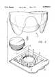
- FIG. 1is a top plan view of a BGA package of the present invention without a heat sink and with portions thereof broken away for illustrative purposes;
- FIG. 2is a cross-sectional view of the package of FIG. 1 taken on line 2--2 and illustrated with a heat sink;
- FIG. 3is a fragmentary perspective view of the package of FIG. 1 mounted on an underlying motherboard with the heat sink shown unthreaded and removed therefrom and a repair station being positioned thereover, the repair station having portions thereof broken away for illustrative purposes;
- FIG. 4is a cross-sectional view showing the package with the repair station of FIG. 3 positioned thereover in a die removal process
- FIG. 5is a view similar to FIG. 4 showing a die replacement process of the invention.
- Package 10includes a BGA substrate 14.
- An integrated circuit die or chip 18is mounted on the substrate 14 and electrically connected thereto by wire bonds 26.
- a lock ring 30is attached to the top of the substrate 14 with Loctite or other adhesive 34. It is attached with the threaded opening 38 thereof surrounding the die 18.
- the threaded opening 38is preferably a one-inch pipe thread.
- Hysol encapsulant 42is poured into the opening to cover the die 18 and wire bonds 26. The encapsulant 42 when cured thereby also secures the lock ring 30 to the substrate 14.
- the lock ring 30can be an electrical box lock nut cast of white metal. They are commercially available retail and are very inexpensive, perhaps ten cents apiece. In large wholesale volumes, the lock nuts would likely cost no more than five cents each.
- steps of a preferred method of constructing the package 10are as follows:
- a die 18is attached to a BGA substrate 14 or more particularly an EPBGA substrate;
- a threaded lock ring 30is positioned on the substrate 14 using a light application of Loctite adhesive 34 to the substrate;
- the threaded opening 38is filled with HYSOL encapsulant to completely cover the wire bonds and the die.
- a threaded heat sink 50as shown in FIGS. 2 and 3, can be screwed into the threaded opening 38.
- the heat sink 50has a male threaded portion 54 and horizontal fins 58 secured thereon.
- An example of a preferred threaded heat sink 50is that available from Vemaline Products.
- the package 10is attached to a printed circuit board or motherboard 62 by reflowing the solder balls 66 of the BGA substrate 14.
- the securement of the package 10 to the motherboard 62is shown in FIG. 3.
- the heat sink 50can be threaded into a secure position in the threaded opening 38 before or preferably after the package 10 is secured to the motherboard 62, as shown in FIG. 3.
- the present inventionallows for easy removal from the motherboard 62 for replacement or removal (for repair), as can be understood from FIGS. 3-5.
- First the heat sink 50is unthreaded from the threaded opening 38 and removed from the package 10.
- the repair station 70is then positioned securely over the package 10, and hot nitrogen gas 74 is pumped in and directed to the solder balls 66. With the solder balls 66 melted or reflowed, the package 10 can be removed from the motherboard 62.
- the heat sink 50can be threaded on and off as many times as needed.
- FIG. 4shows the repair station 70 in position in a component (package 10 or die 18) removal process. Since the heat sink 50 has been removed, the vacuum tube 78 can efficiently access the component. Thereby a suction removal pressure applied thereto by the tube 78 and with the solder balls melted by the hot air as shown by the squiggly arrows 74 allows removal of the component off of the board 62.
- the outer nozzle 86prevents neighboring components on the board 62 from being heated.
- the repair station inner nozzle 90helps form desirable hot air flow paths.
- the packageis positioned at the desired location on the board with the solder balls 66 thereagainst.
- the repair station 70is positioned over it, and the hot air 74 injected down and around and under to heat and reflow the solder balls 66, thereby mounting the package 10 to the board.
- the nozzles 86, 90 of the repair station 70efficiently direct the hot air to the solder balls 66 without heating adjacent components.
- the present inventionprovides a secure locking mechanism for attaching a threaded heat sink 50 to the top of an EPBGA package 10.
- the package 10is very inexpensive. It also allows the customer end user the ability to remove and/or replace at their discretion the defective component for repair or replacement. This is accomplished by building into the package 10 an inexpensive lock ring 30, which can be easily adhered to the substrate 14 by the encapsulant 42 covering the wire bonds 26.
Landscapes
- Physics & Mathematics (AREA)
- Condensed Matter Physics & Semiconductors (AREA)
- General Physics & Mathematics (AREA)
- Engineering & Computer Science (AREA)
- Computer Hardware Design (AREA)
- Microelectronics & Electronic Packaging (AREA)
- Power Engineering (AREA)
- Chemical & Material Sciences (AREA)
- Dispersion Chemistry (AREA)
- Electric Connection Of Electric Components To Printed Circuits (AREA)
Abstract
Description
Claims (27)
Priority Applications (2)
| Application Number | Priority Date | Filing Date | Title |
|---|---|---|---|
| US08/724,076US5789813A (en) | 1996-09-30 | 1996-09-30 | Ball grid array package with inexpensive threaded secure locking mechanism to allow removal of a threaded heat sink therefrom |
| US08/901,489US5885848A (en) | 1996-09-30 | 1997-07-28 | Ball grid array with inexpensive threaded secure locking mechanism to allow removal of a threaded heat sink therefrom |
Applications Claiming Priority (1)
| Application Number | Priority Date | Filing Date | Title |
|---|---|---|---|
| US08/724,076US5789813A (en) | 1996-09-30 | 1996-09-30 | Ball grid array package with inexpensive threaded secure locking mechanism to allow removal of a threaded heat sink therefrom |
Related Child Applications (1)
| Application Number | Title | Priority Date | Filing Date |
|---|---|---|---|
| US08/901,489DivisionUS5885848A (en) | 1996-09-30 | 1997-07-28 | Ball grid array with inexpensive threaded secure locking mechanism to allow removal of a threaded heat sink therefrom |
Publications (1)
| Publication Number | Publication Date |
|---|---|
| US5789813Atrue US5789813A (en) | 1998-08-04 |
Family
ID=24908878
Family Applications (2)
| Application Number | Title | Priority Date | Filing Date |
|---|---|---|---|
| US08/724,076Expired - LifetimeUS5789813A (en) | 1996-09-30 | 1996-09-30 | Ball grid array package with inexpensive threaded secure locking mechanism to allow removal of a threaded heat sink therefrom |
| US08/901,489Expired - Fee RelatedUS5885848A (en) | 1996-09-30 | 1997-07-28 | Ball grid array with inexpensive threaded secure locking mechanism to allow removal of a threaded heat sink therefrom |
Family Applications After (1)
| Application Number | Title | Priority Date | Filing Date |
|---|---|---|---|
| US08/901,489Expired - Fee RelatedUS5885848A (en) | 1996-09-30 | 1997-07-28 | Ball grid array with inexpensive threaded secure locking mechanism to allow removal of a threaded heat sink therefrom |
Country Status (1)
| Country | Link |
|---|---|
| US (2) | US5789813A (en) |
Cited By (21)
| Publication number | Priority date | Publication date | Assignee | Title |
|---|---|---|---|---|
| US2795151A (en)* | 1953-08-03 | 1957-06-11 | Heagerty Hubert | Vehicle throttle depressor |
| US5898571A (en)* | 1997-04-28 | 1999-04-27 | Lsi Logic Corporation | Apparatus and method for clip-on attachment of heat sinks to encapsulated semiconductor packages |
| US5945736A (en)* | 1998-09-28 | 1999-08-31 | Chip Coolers, Inc. | Heat sink assembly with snap-in cover plate having multiple pressure capability |
| US5977622A (en)* | 1997-04-25 | 1999-11-02 | Lsi Logic Corporation | Stiffener with slots for clip-on heat sink attachment |
| US6229702B1 (en)* | 1999-06-02 | 2001-05-08 | Advanced Semiconductor Engineering, Inc. | Ball grid array semiconductor package having improved heat dissipation efficiency, overall electrical performance and enhanced bonding capability |
| US6355985B1 (en)* | 1998-10-01 | 2002-03-12 | Micron Technology, Inc. | Integrated circuit device and synchronous-link dynamic random access memory device |
| US6373703B2 (en) | 1997-12-17 | 2002-04-16 | International Business Machines Corporation | Integral design features for heatsink attach for electronic packages |
| US6515360B2 (en)* | 1999-07-28 | 2003-02-04 | Mitsubishi Denki Kabushiki Kaisha | Packaged semiconductor device and manufacturing method thereof |
| US20030141349A1 (en)* | 2002-01-26 | 2003-07-31 | Wenzhong Liu | SBB HGA rework process |
| USD478556S1 (en) | 2002-01-10 | 2003-08-19 | Nasser Abo Abdo | Speaker heat sink |
| US20030178719A1 (en)* | 2002-03-22 | 2003-09-25 | Combs Edward G. | Enhanced thermal dissipation integrated circuit package and method of manufacturing enhanced thermal dissipation integrated circuit package |
| US6734552B2 (en) | 2001-07-11 | 2004-05-11 | Asat Limited | Enhanced thermal dissipation integrated circuit package |
| US20040263007A1 (en)* | 2003-05-19 | 2004-12-30 | Wetherill Associates, Inc. | Thermal transfer container for semiconductor component |
| US20050265000A1 (en)* | 2004-05-26 | 2005-12-01 | Foxconn Technology Co., Ltd. | Heat sink assembly with fixing devices |
| US7015072B2 (en) | 2001-07-11 | 2006-03-21 | Asat Limited | Method of manufacturing an enhanced thermal dissipation integrated circuit package |
| US20070080471A1 (en)* | 2005-10-12 | 2007-04-12 | Sony Computer Entertainment Inc. | Semiconductor device, method for assembling semiconductor device |
| US20070119571A1 (en)* | 2005-11-30 | 2007-05-31 | Fujitsu Limited | Electronic device cooling apparatus |
| US20070158796A1 (en)* | 2005-12-09 | 2007-07-12 | International Rectifier Corporation | Semiconductor package |
| US20100200984A1 (en)* | 2009-02-12 | 2010-08-12 | Honeywell International Inc. | Adjustable threaded cores for led thermal management |
| US20170084508A1 (en)* | 2015-09-17 | 2017-03-23 | Fuji Electric Co., Ltd. | Semiconductor device and electrical device |
| US20170229374A1 (en)* | 2016-02-10 | 2017-08-10 | International Business Machines Corporation | Heat sink with integrated threaded lid |
Families Citing this family (5)
| Publication number | Priority date | Publication date | Assignee | Title |
|---|---|---|---|---|
| US6196439B1 (en)* | 1998-05-29 | 2001-03-06 | International Business Machines Corporation | Method and apparatus for μBGA removal and reattach |
| US6091603A (en)* | 1999-09-30 | 2000-07-18 | International Business Machines Corporation | Customizable lid for improved thermal performance of modules using flip chips |
| US6292369B1 (en) | 2000-08-07 | 2001-09-18 | International Business Machines Corporation | Methods for customizing lid for improved thermal performance of modules using flip chips |
| WO2015012792A1 (en)* | 2013-07-22 | 2015-01-29 | Ge Intelligent Platforms, Inc. | Screw plug adjustable heat sinks and methods of fabricating the same |
| EP4092720A1 (en)* | 2021-05-20 | 2022-11-23 | Aptiv Technologies Limited | Heat sink |
Citations (14)
| Publication number | Priority date | Publication date | Assignee | Title |
|---|---|---|---|---|
| US4612978A (en)* | 1983-07-14 | 1986-09-23 | Cutchaw John M | Apparatus for cooling high-density integrated circuit packages |
| US4748495A (en)* | 1985-08-08 | 1988-05-31 | Dypax Systems Corporation | High density multi-chip interconnection and cooling package |
| US4884169A (en)* | 1989-01-23 | 1989-11-28 | Technology Enterprises Company | Bubble generation in condensation wells for cooling high density integrated circuit chips |
| US5227663A (en)* | 1989-12-19 | 1993-07-13 | Lsi Logic Corporation | Integral dam and heat sink for semiconductor device assembly |
| US5285352A (en)* | 1992-07-15 | 1994-02-08 | Motorola, Inc. | Pad array semiconductor device with thermal conductor and process for making the same |
| US5293930A (en)* | 1992-09-24 | 1994-03-15 | Hewlett-Packard Company | Surface-to-air heat exchanger for electronic devices |
| US5311060A (en)* | 1989-12-19 | 1994-05-10 | Lsi Logic Corporation | Heat sink for semiconductor device assembly |
| US5355283A (en)* | 1993-04-14 | 1994-10-11 | Amkor Electronics, Inc. | Ball grid array with via interconnection |
| US5386342A (en)* | 1992-01-30 | 1995-01-31 | Lsi Logic Corporation | Rigid backplane formed from a moisture resistant insulative material used to protect a semiconductor device |
| US5397919A (en)* | 1993-03-04 | 1995-03-14 | Square Head, Inc. | Heat sink assembly for solid state devices |
| US5525835A (en)* | 1991-08-08 | 1996-06-11 | Sumitomo Electric Industries, Ltd. | Semiconductor chip module having an electrically insulative thermally conductive thermal dissipator directly in contact with the semiconductor element |
| US5528159A (en)* | 1993-06-14 | 1996-06-18 | International Business Machine Corp. | Method and apparatus for testing integrated circuit chips |
| US5610442A (en)* | 1995-03-27 | 1997-03-11 | Lsi Logic Corporation | Semiconductor device package fabrication method and apparatus |
| US5619070A (en)* | 1993-12-28 | 1997-04-08 | Kabushiki Kaisha Toshiba | Semiconductor device which radiates heat and applies substrate potential from rear surface of semiconductor chip |
Family Cites Families (6)
| Publication number | Priority date | Publication date | Assignee | Title |
|---|---|---|---|---|
| JPH0472747A (en)* | 1990-07-13 | 1992-03-06 | Fujitsu Ltd | Semiconductor device |
| US5204287A (en)* | 1991-06-28 | 1993-04-20 | Texas Instruments Incorporated | Integrated circuit device having improved post for surface-mount package |
| US5451274A (en)* | 1994-01-31 | 1995-09-19 | Motorola, Inc. | Reflow of multi-layer metal bumps |
| US5467253A (en)* | 1994-06-30 | 1995-11-14 | Motorola, Inc. | Semiconductor chip package and method of forming |
| US5620928A (en)* | 1995-05-11 | 1997-04-15 | National Semiconductor Corporation | Ultra thin ball grid array using a flex tape or printed wiring board substrate and method |
| US5672547A (en)* | 1996-01-31 | 1997-09-30 | Industrial Technology Research Institute | Method for bonding a heat sink to a die paddle |
- 1996
- 1996-09-30USUS08/724,076patent/US5789813A/ennot_activeExpired - Lifetime
- 1997
- 1997-07-28USUS08/901,489patent/US5885848A/ennot_activeExpired - Fee Related
Patent Citations (14)
| Publication number | Priority date | Publication date | Assignee | Title |
|---|---|---|---|---|
| US4612978A (en)* | 1983-07-14 | 1986-09-23 | Cutchaw John M | Apparatus for cooling high-density integrated circuit packages |
| US4748495A (en)* | 1985-08-08 | 1988-05-31 | Dypax Systems Corporation | High density multi-chip interconnection and cooling package |
| US4884169A (en)* | 1989-01-23 | 1989-11-28 | Technology Enterprises Company | Bubble generation in condensation wells for cooling high density integrated circuit chips |
| US5311060A (en)* | 1989-12-19 | 1994-05-10 | Lsi Logic Corporation | Heat sink for semiconductor device assembly |
| US5227663A (en)* | 1989-12-19 | 1993-07-13 | Lsi Logic Corporation | Integral dam and heat sink for semiconductor device assembly |
| US5525835A (en)* | 1991-08-08 | 1996-06-11 | Sumitomo Electric Industries, Ltd. | Semiconductor chip module having an electrically insulative thermally conductive thermal dissipator directly in contact with the semiconductor element |
| US5386342A (en)* | 1992-01-30 | 1995-01-31 | Lsi Logic Corporation | Rigid backplane formed from a moisture resistant insulative material used to protect a semiconductor device |
| US5285352A (en)* | 1992-07-15 | 1994-02-08 | Motorola, Inc. | Pad array semiconductor device with thermal conductor and process for making the same |
| US5293930A (en)* | 1992-09-24 | 1994-03-15 | Hewlett-Packard Company | Surface-to-air heat exchanger for electronic devices |
| US5397919A (en)* | 1993-03-04 | 1995-03-14 | Square Head, Inc. | Heat sink assembly for solid state devices |
| US5355283A (en)* | 1993-04-14 | 1994-10-11 | Amkor Electronics, Inc. | Ball grid array with via interconnection |
| US5528159A (en)* | 1993-06-14 | 1996-06-18 | International Business Machine Corp. | Method and apparatus for testing integrated circuit chips |
| US5619070A (en)* | 1993-12-28 | 1997-04-08 | Kabushiki Kaisha Toshiba | Semiconductor device which radiates heat and applies substrate potential from rear surface of semiconductor chip |
| US5610442A (en)* | 1995-03-27 | 1997-03-11 | Lsi Logic Corporation | Semiconductor device package fabrication method and apparatus |
Cited By (31)
| Publication number | Priority date | Publication date | Assignee | Title |
|---|---|---|---|---|
| US2795151A (en)* | 1953-08-03 | 1957-06-11 | Heagerty Hubert | Vehicle throttle depressor |
| US5977622A (en)* | 1997-04-25 | 1999-11-02 | Lsi Logic Corporation | Stiffener with slots for clip-on heat sink attachment |
| US5898571A (en)* | 1997-04-28 | 1999-04-27 | Lsi Logic Corporation | Apparatus and method for clip-on attachment of heat sinks to encapsulated semiconductor packages |
| US6373703B2 (en) | 1997-12-17 | 2002-04-16 | International Business Machines Corporation | Integral design features for heatsink attach for electronic packages |
| US5945736A (en)* | 1998-09-28 | 1999-08-31 | Chip Coolers, Inc. | Heat sink assembly with snap-in cover plate having multiple pressure capability |
| US6706565B2 (en) | 1998-10-01 | 2004-03-16 | Micron Technology, Inc. | Methods of forming an integrated circuit device |
| US6949838B2 (en) | 1998-10-01 | 2005-09-27 | Micron Technology, Inc. | Integrated circuit device |
| US6355985B1 (en)* | 1998-10-01 | 2002-03-12 | Micron Technology, Inc. | Integrated circuit device and synchronous-link dynamic random access memory device |
| US6229702B1 (en)* | 1999-06-02 | 2001-05-08 | Advanced Semiconductor Engineering, Inc. | Ball grid array semiconductor package having improved heat dissipation efficiency, overall electrical performance and enhanced bonding capability |
| US6515360B2 (en)* | 1999-07-28 | 2003-02-04 | Mitsubishi Denki Kabushiki Kaisha | Packaged semiconductor device and manufacturing method thereof |
| US6734552B2 (en) | 2001-07-11 | 2004-05-11 | Asat Limited | Enhanced thermal dissipation integrated circuit package |
| US7015072B2 (en) | 2001-07-11 | 2006-03-21 | Asat Limited | Method of manufacturing an enhanced thermal dissipation integrated circuit package |
| USD478556S1 (en) | 2002-01-10 | 2003-08-19 | Nasser Abo Abdo | Speaker heat sink |
| US20030141349A1 (en)* | 2002-01-26 | 2003-07-31 | Wenzhong Liu | SBB HGA rework process |
| CN1316451C (en)* | 2002-01-26 | 2007-05-16 | 新科实业有限公司 | Reprocessing process of SBB HGA |
| US20030178719A1 (en)* | 2002-03-22 | 2003-09-25 | Combs Edward G. | Enhanced thermal dissipation integrated circuit package and method of manufacturing enhanced thermal dissipation integrated circuit package |
| US20040046241A1 (en)* | 2002-03-22 | 2004-03-11 | Combs Edward G. | Method of manufacturing enhanced thermal dissipation integrated circuit package |
| US20040263007A1 (en)* | 2003-05-19 | 2004-12-30 | Wetherill Associates, Inc. | Thermal transfer container for semiconductor component |
| US20080042501A1 (en)* | 2003-05-19 | 2008-02-21 | Robert Malanga | Thermal transfer container for semiconductor component |
| US20050265000A1 (en)* | 2004-05-26 | 2005-12-01 | Foxconn Technology Co., Ltd. | Heat sink assembly with fixing devices |
| US7683479B2 (en)* | 2005-10-12 | 2010-03-23 | Sony Computer Entertainment Inc. | Semiconductor package involving a rotary lock that connects a package substrate and a separate component |
| US20070080471A1 (en)* | 2005-10-12 | 2007-04-12 | Sony Computer Entertainment Inc. | Semiconductor device, method for assembling semiconductor device |
| US8230901B2 (en)* | 2005-11-30 | 2012-07-31 | Fujitsu Limited | Electronic device cooling apparatus |
| US20070119571A1 (en)* | 2005-11-30 | 2007-05-31 | Fujitsu Limited | Electronic device cooling apparatus |
| US20070158796A1 (en)* | 2005-12-09 | 2007-07-12 | International Rectifier Corporation | Semiconductor package |
| US20100200984A1 (en)* | 2009-02-12 | 2010-08-12 | Honeywell International Inc. | Adjustable threaded cores for led thermal management |
| US7898077B2 (en)* | 2009-02-12 | 2011-03-01 | Honeywell International Inc. | Adjustable threaded cores for LED thermal management |
| US20170084508A1 (en)* | 2015-09-17 | 2017-03-23 | Fuji Electric Co., Ltd. | Semiconductor device and electrical device |
| US9905489B2 (en)* | 2015-09-17 | 2018-02-27 | Fuji Electric Co., Ltd. | Semiconductor device and electrical device |
| US20170229374A1 (en)* | 2016-02-10 | 2017-08-10 | International Business Machines Corporation | Heat sink with integrated threaded lid |
| US10002819B2 (en)* | 2016-02-10 | 2018-06-19 | International Business Machines Corporation | Heat sink with integrated threaded lid |
Also Published As
| Publication number | Publication date |
|---|---|
| US5885848A (en) | 1999-03-23 |
Similar Documents
| Publication | Publication Date | Title |
|---|---|---|
| US5789813A (en) | Ball grid array package with inexpensive threaded secure locking mechanism to allow removal of a threaded heat sink therefrom | |
| US7078803B2 (en) | Integrated circuit heat dissipation system | |
| US6317326B1 (en) | Integrated circuit device package and heat dissipation device | |
| US6617684B2 (en) | Packaged die on PCB with heat sink encapsulant | |
| US6963130B1 (en) | Heatsinking and packaging of integrated circuit chips | |
| US7126218B1 (en) | Embedded heat spreader ball grid array | |
| US6190945B1 (en) | Integrated heat sink | |
| US5693572A (en) | Ball grid array integrated circuit package with high thermal conductivity | |
| US5590462A (en) | Process for dissipating heat from a semiconductor package | |
| US7078806B2 (en) | IC die support structures for ball grid array package fabrication | |
| US8525326B2 (en) | IC package with capacitors disposed on an interposal layer | |
| US7342304B2 (en) | Semiconductor package with heat dissipating structure | |
| US6255140B1 (en) | Flip chip chip-scale package | |
| US6728106B2 (en) | Heat dissipation structure of integrated circuit (IC) | |
| KR19980047710A (en) | Stacked semiconductor package and assembly method thereof | |
| US7315079B2 (en) | Thermally-enhanced ball grid array package structure and method | |
| US6559537B1 (en) | Ball grid array packages with thermally conductive containers | |
| US5457878A (en) | Method for mounting integrated circuit chips on a mini-board | |
| US6558981B2 (en) | Method for making an encapsulated semiconductor chip module | |
| US5488539A (en) | Protecting cot packaged ICs during wave solder operations | |
| US6403896B1 (en) | Substrate having specific pad distribution | |
| JPH02170494A (en) | Electronic circuit package | |
| US20050139994A1 (en) | Semiconductor package | |
| US20040173903A1 (en) | Thin type ball grid array package | |
| KR0144311B1 (en) | Cap-type ball grid array semiconductor package and manufacturing method thereof |
Legal Events
| Date | Code | Title | Description |
|---|---|---|---|
| AS | Assignment | Owner name:LSI LOGIC CORPORATION, CALIFORNIA Free format text:ASSIGNMENT OF ASSIGNORS INTEREST;ASSIGNORS:KIRKLAND, JANET;SCHNEIDER, MARK R.;REEL/FRAME:008288/0401 Effective date:19961114 | |
| STCF | Information on status: patent grant | Free format text:PATENTED CASE | |
| FPAY | Fee payment | Year of fee payment:4 | |
| FPAY | Fee payment | Year of fee payment:8 | |
| FEPP | Fee payment procedure | Free format text:PAYOR NUMBER ASSIGNED (ORIGINAL EVENT CODE: ASPN); ENTITY STATUS OF PATENT OWNER: LARGE ENTITY Free format text:PAYER NUMBER DE-ASSIGNED (ORIGINAL EVENT CODE: RMPN); ENTITY STATUS OF PATENT OWNER: LARGE ENTITY | |
| FPAY | Fee payment | Year of fee payment:12 | |
| AS | Assignment | Owner name:DEUTSCHE BANK AG NEW YORK BRANCH, AS COLLATERAL AG Free format text:PATENT SECURITY AGREEMENT;ASSIGNORS:LSI CORPORATION;AGERE SYSTEMS LLC;REEL/FRAME:032856/0031 Effective date:20140506 | |
| AS | Assignment | Owner name:LSI CORPORATION, CALIFORNIA Free format text:CHANGE OF NAME;ASSIGNOR:LSI LOGIC CORPORATION;REEL/FRAME:033102/0270 Effective date:20070406 | |
| AS | Assignment | Owner name:AVAGO TECHNOLOGIES GENERAL IP (SINGAPORE) PTE. LTD Free format text:ASSIGNMENT OF ASSIGNORS INTEREST;ASSIGNOR:LSI CORPORATION;REEL/FRAME:035390/0388 Effective date:20140814 | |
| AS | Assignment | Owner name:LSI CORPORATION, CALIFORNIA Free format text:TERMINATION AND RELEASE OF SECURITY INTEREST IN PATENT RIGHTS (RELEASES RF 032856-0031);ASSIGNOR:DEUTSCHE BANK AG NEW YORK BRANCH, AS COLLATERAL AGENT;REEL/FRAME:037684/0039 Effective date:20160201 Owner name:AGERE SYSTEMS LLC, PENNSYLVANIA Free format text:TERMINATION AND RELEASE OF SECURITY INTEREST IN PATENT RIGHTS (RELEASES RF 032856-0031);ASSIGNOR:DEUTSCHE BANK AG NEW YORK BRANCH, AS COLLATERAL AGENT;REEL/FRAME:037684/0039 Effective date:20160201 | |
| AS | Assignment | Owner name:BANK OF AMERICA, N.A., AS COLLATERAL AGENT, NORTH CAROLINA Free format text:PATENT SECURITY AGREEMENT;ASSIGNOR:AVAGO TECHNOLOGIES GENERAL IP (SINGAPORE) PTE. LTD.;REEL/FRAME:037808/0001 Effective date:20160201 Owner name:BANK OF AMERICA, N.A., AS COLLATERAL AGENT, NORTH Free format text:PATENT SECURITY AGREEMENT;ASSIGNOR:AVAGO TECHNOLOGIES GENERAL IP (SINGAPORE) PTE. LTD.;REEL/FRAME:037808/0001 Effective date:20160201 | |
| AS | Assignment | Owner name:AVAGO TECHNOLOGIES GENERAL IP (SINGAPORE) PTE. LTD., SINGAPORE Free format text:TERMINATION AND RELEASE OF SECURITY INTEREST IN PATENTS;ASSIGNOR:BANK OF AMERICA, N.A., AS COLLATERAL AGENT;REEL/FRAME:041710/0001 Effective date:20170119 Owner name:AVAGO TECHNOLOGIES GENERAL IP (SINGAPORE) PTE. LTD Free format text:TERMINATION AND RELEASE OF SECURITY INTEREST IN PATENTS;ASSIGNOR:BANK OF AMERICA, N.A., AS COLLATERAL AGENT;REEL/FRAME:041710/0001 Effective date:20170119 | |
| AS | Assignment | Owner name:CORTLAND CAPITAL MARKET SERVICES LLC, AS COLLATERA Free format text:SECURITY INTEREST;ASSIGNORS:HILCO PATENT ACQUISITION 56, LLC;BELL SEMICONDUCTOR, LLC;BELL NORTHERN RESEARCH, LLC;REEL/FRAME:045216/0020 Effective date:20180124 | |
| AS | Assignment | Owner name:BELL SEMICONDUCTOR, LLC, ILLINOIS Free format text:ASSIGNMENT OF ASSIGNORS INTEREST;ASSIGNORS:AVAGO TECHNOLOGIES GENERAL IP (SINGAPORE) PTE. LTD.;BROADCOM CORPORATION;REEL/FRAME:050635/0001 Effective date:20171208 |