US5789068A - Preformed solder parts coated with parylene in a thickness effective to exhibit predetermined interference colors - Google Patents
Preformed solder parts coated with parylene in a thickness effective to exhibit predetermined interference colorsDownload PDFInfo
- Publication number
- US5789068A US5789068AUS08/498,247US49824795AUS5789068AUS 5789068 AUS5789068 AUS 5789068AUS 49824795 AUS49824795 AUS 49824795AUS 5789068 AUS5789068 AUS 5789068A
- Authority
- US
- United States
- Prior art keywords
- solder preform
- transparent material
- color
- solder
- poly
- Prior art date
- Legal status (The legal status is an assumption and is not a legal conclusion. Google has not performed a legal analysis and makes no representation as to the accuracy of the status listed.)
- Expired - Lifetime
Links
- 229910000679solderInorganic materials0.000titleclaimsabstractdescription114
- 229920000052poly(p-xylylene)Polymers0.000titleclaimsabstractdescription76
- 239000003086colorantSubstances0.000titleabstractdescription19
- 238000000034methodMethods0.000claimsabstractdescription44
- 238000000576coating methodMethods0.000claimsabstractdescription36
- 239000011248coating agentSubstances0.000claimsabstractdescription35
- 238000004519manufacturing processMethods0.000claimsabstractdescription18
- 230000000007visual effectEffects0.000claimsabstractdescription4
- 238000010438heat treatmentMethods0.000claimsabstract3
- 230000008018meltingEffects0.000claimsdescription25
- 238000002844meltingMethods0.000claimsdescription25
- 239000000463materialSubstances0.000claimsdescription23
- 230000004907fluxEffects0.000claimsdescription17
- 230000001066destructive effectEffects0.000claimsdescription16
- 239000007788liquidSubstances0.000claimsdescription11
- 238000009500colour coatingMethods0.000claimsdescription2
- 239000012780transparent materialSubstances0.000claims35
- 238000004040coloringMethods0.000claims1
- 229910045601alloyInorganic materials0.000abstractdescription9
- 239000000956alloySubstances0.000abstractdescription9
- 230000008569processEffects0.000abstractdescription7
- 230000008859changeEffects0.000abstractdescription6
- 230000003287optical effectEffects0.000abstractdescription5
- PCHJSUWPFVWCPO-UHFFFAOYSA-NgoldChemical compound[Au]PCHJSUWPFVWCPO-UHFFFAOYSA-N0.000abstractdescription2
- 229910052737goldInorganic materials0.000abstractdescription2
- 239000010931goldSubstances0.000abstractdescription2
- 239000000203mixtureSubstances0.000abstractdescription2
- 239000010408filmSubstances0.000description15
- 239000000758substrateSubstances0.000description6
- BQCADISMDOOEFD-UHFFFAOYSA-NSilverChemical compound[Ag]BQCADISMDOOEFD-UHFFFAOYSA-N0.000description5
- 229910052709silverInorganic materials0.000description5
- 239000004332silverSubstances0.000description5
- 239000010409thin filmSubstances0.000description5
- 230000008021depositionEffects0.000description4
- 238000000151depositionMethods0.000description4
- 239000000178monomerSubstances0.000description4
- 229920000642polymerPolymers0.000description4
- 230000000712assemblyEffects0.000description3
- 238000000429assemblyMethods0.000description3
- 230000000694effectsEffects0.000description3
- XLYOFNOQVPJJNP-UHFFFAOYSA-NwaterSubstancesOXLYOFNOQVPJJNP-UHFFFAOYSA-N0.000description3
- ATJFFYVFTNAWJD-UHFFFAOYSA-NTinChemical compound[Sn]ATJFFYVFTNAWJD-UHFFFAOYSA-N0.000description2
- 230000003111delayed effectEffects0.000description2
- 239000000539dimerSubstances0.000description2
- 239000011521glassSubstances0.000description2
- 239000000155meltSubstances0.000description2
- 229910052751metalInorganic materials0.000description2
- 239000002184metalSubstances0.000description2
- 150000002739metalsChemical class0.000description2
- 230000000717retained effectEffects0.000description2
- XOLBLPGZBRYERU-UHFFFAOYSA-Ntin dioxideChemical compoundO=[Sn]=OXOLBLPGZBRYERU-UHFFFAOYSA-N0.000description2
- 229910001887tin oxideInorganic materials0.000description2
- 238000005019vapor deposition processMethods0.000description2
- OOLUVSIJOMLOCB-UHFFFAOYSA-N1633-22-3Chemical compoundC1CC(C=C2)=CC=C2CCC2=CC=C1C=C2OOLUVSIJOMLOCB-UHFFFAOYSA-N0.000description1
- 101100386054Saccharomyces cerevisiae (strain ATCC 204508 / S288c) CYS3 geneProteins0.000description1
- 229910052787antimonyInorganic materials0.000description1
- WATWJIUSRGPENY-UHFFFAOYSA-Nantimony atomChemical compound[Sb]WATWJIUSRGPENY-UHFFFAOYSA-N0.000description1
- QVGXLLKOCUKJST-UHFFFAOYSA-Natomic oxygenChemical compound[O]QVGXLLKOCUKJST-UHFFFAOYSA-N0.000description1
- 230000005540biological transmissionEffects0.000description1
- VQLYBLABXAHUDN-UHFFFAOYSA-Nbis(4-fluorophenyl)-methyl-(1,2,4-triazol-1-ylmethyl)silane;methyl n-(1h-benzimidazol-2-yl)carbamateChemical compoundC1=CC=C2NC(NC(=O)OC)=NC2=C1.C=1C=C(F)C=CC=1[Si](C=1C=CC(F)=CC=1)(C)CN1C=NC=N1VQLYBLABXAHUDN-UHFFFAOYSA-N0.000description1
- 229910052797bismuthInorganic materials0.000description1
- JCXGWMGPZLAOME-UHFFFAOYSA-Nbismuth atomChemical compound[Bi]JCXGWMGPZLAOME-UHFFFAOYSA-N0.000description1
- 229910052793cadmiumInorganic materials0.000description1
- BDOSMKKIYDKNTQ-UHFFFAOYSA-Ncadmium atomChemical compound[Cd]BDOSMKKIYDKNTQ-UHFFFAOYSA-N0.000description1
- 230000000052comparative effectEffects0.000description1
- 239000002131composite materialSubstances0.000description1
- 229920001577copolymerPolymers0.000description1
- 238000005137deposition processMethods0.000description1
- 239000006023eutectic alloySubstances0.000description1
- 239000007888film coatingSubstances0.000description1
- 238000009501film coatingMethods0.000description1
- 229910052738indiumInorganic materials0.000description1
- APFVFJFRJDLVQX-UHFFFAOYSA-Nindium atomChemical compound[In]APFVFJFRJDLVQX-UHFFFAOYSA-N0.000description1
- LQBJWKCYZGMFEV-UHFFFAOYSA-Nlead tinChemical compound[Sn].[Pb]LQBJWKCYZGMFEV-UHFFFAOYSA-N0.000description1
- 229910044991metal oxideInorganic materials0.000description1
- 150000004706metal oxidesChemical class0.000description1
- 230000004048modificationEffects0.000description1
- 238000012986modificationMethods0.000description1
- 239000012299nitrogen atmosphereSubstances0.000description1
- 239000001301oxygenSubstances0.000description1
- 229910052760oxygenInorganic materials0.000description1
- DDSPUNTXKUFWTM-UHFFFAOYSA-Noxygen(2-);tin(4+)Chemical compound[O-2].[O-2].[Sn+4]DDSPUNTXKUFWTM-UHFFFAOYSA-N0.000description1
- 230000037361pathwayEffects0.000description1
- 230000010363phase shiftEffects0.000description1
- 238000002360preparation methodMethods0.000description1
- 238000000197pyrolysisMethods0.000description1
- 230000008707rearrangementEffects0.000description1
- 230000002787reinforcementEffects0.000description1
- 239000000344soapSubstances0.000description1
- 238000005476solderingMethods0.000description1
- 239000002195soluble materialSubstances0.000description1
- 239000007858starting materialSubstances0.000description1
- 101150035983str1 geneProteins0.000description1
- 239000000126substanceSubstances0.000description1
- 229910001174tin-lead alloyInorganic materials0.000description1
- 238000002834transmittanceMethods0.000description1
- 230000008016vaporizationEffects0.000description1
- 238000009834vaporizationMethods0.000description1
Images

Classifications
- H—ELECTRICITY
- H05—ELECTRIC TECHNIQUES NOT OTHERWISE PROVIDED FOR
- H05K—PRINTED CIRCUITS; CASINGS OR CONSTRUCTIONAL DETAILS OF ELECTRIC APPARATUS; MANUFACTURE OF ASSEMBLAGES OF ELECTRICAL COMPONENTS
- H05K3/00—Apparatus or processes for manufacturing printed circuits
- H05K3/30—Assembling printed circuits with electric components, e.g. with resistor
- H05K3/32—Assembling printed circuits with electric components, e.g. with resistor electrically connecting electric components or wires to printed circuits
- H05K3/34—Assembling printed circuits with electric components, e.g. with resistor electrically connecting electric components or wires to printed circuits by soldering
- H05K3/341—Surface mounted components
- H05K3/3431—Leadless components
- H05K3/3436—Leadless components having an array of bottom contacts, e.g. pad grid array or ball grid array components
- B—PERFORMING OPERATIONS; TRANSPORTING
- B23—MACHINE TOOLS; METAL-WORKING NOT OTHERWISE PROVIDED FOR
- B23K—SOLDERING OR UNSOLDERING; WELDING; CLADDING OR PLATING BY SOLDERING OR WELDING; CUTTING BY APPLYING HEAT LOCALLY, e.g. FLAME CUTTING; WORKING BY LASER BEAM
- B23K35/00—Rods, electrodes, materials, or media, for use in soldering, welding, or cutting
- B23K35/02—Rods, electrodes, materials, or media, for use in soldering, welding, or cutting characterised by mechanical features, e.g. shape
- B23K35/0222—Rods, electrodes, materials, or media, for use in soldering, welding, or cutting characterised by mechanical features, e.g. shape for use in soldering, brazing
- B23K35/0244—Powders, particles or spheres; Preforms made therefrom
- B—PERFORMING OPERATIONS; TRANSPORTING
- B23—MACHINE TOOLS; METAL-WORKING NOT OTHERWISE PROVIDED FOR
- B23K—SOLDERING OR UNSOLDERING; WELDING; CLADDING OR PLATING BY SOLDERING OR WELDING; CUTTING BY APPLYING HEAT LOCALLY, e.g. FLAME CUTTING; WORKING BY LASER BEAM
- B23K2101/00—Articles made by soldering, welding or cutting
- B23K2101/36—Electric or electronic devices
- B—PERFORMING OPERATIONS; TRANSPORTING
- B23—MACHINE TOOLS; METAL-WORKING NOT OTHERWISE PROVIDED FOR
- B23K—SOLDERING OR UNSOLDERING; WELDING; CLADDING OR PLATING BY SOLDERING OR WELDING; CUTTING BY APPLYING HEAT LOCALLY, e.g. FLAME CUTTING; WORKING BY LASER BEAM
- B23K35/00—Rods, electrodes, materials, or media, for use in soldering, welding, or cutting
- B23K35/22—Rods, electrodes, materials, or media, for use in soldering, welding, or cutting characterised by the composition or nature of the material
- B23K35/36—Selection of non-metallic compositions, e.g. coatings, fluxes; Selection of soldering or welding materials, conjoint with selection of non-metallic compositions, both selections being of interest
- B23K35/365—Selection of non-metallic compositions of coating materials either alone or conjoint with selection of soldering or welding materials
- H—ELECTRICITY
- H05—ELECTRIC TECHNIQUES NOT OTHERWISE PROVIDED FOR
- H05K—PRINTED CIRCUITS; CASINGS OR CONSTRUCTIONAL DETAILS OF ELECTRIC APPARATUS; MANUFACTURE OF ASSEMBLAGES OF ELECTRICAL COMPONENTS
- H05K1/00—Printed circuits
- H05K1/02—Details
- H05K1/0266—Marks, test patterns or identification means
- H05K1/0269—Marks, test patterns or identification means for visual or optical inspection
- H—ELECTRICITY
- H05—ELECTRIC TECHNIQUES NOT OTHERWISE PROVIDED FOR
- H05K—PRINTED CIRCUITS; CASINGS OR CONSTRUCTIONAL DETAILS OF ELECTRIC APPARATUS; MANUFACTURE OF ASSEMBLAGES OF ELECTRICAL COMPONENTS
- H05K2201/00—Indexing scheme relating to printed circuits covered by H05K1/00
- H05K2201/01—Dielectrics
- H05K2201/0137—Materials
- H05K2201/0179—Thin film deposited insulating layer, e.g. inorganic layer for printed capacitor
- H—ELECTRICITY
- H05—ELECTRIC TECHNIQUES NOT OTHERWISE PROVIDED FOR
- H05K—PRINTED CIRCUITS; CASINGS OR CONSTRUCTIONAL DETAILS OF ELECTRIC APPARATUS; MANUFACTURE OF ASSEMBLAGES OF ELECTRICAL COMPONENTS
- H05K2203/00—Indexing scheme relating to apparatus or processes for manufacturing printed circuits covered by H05K3/00
- H05K2203/04—Soldering or other types of metallurgic bonding
- H05K2203/041—Solder preforms in the shape of solder balls
- H—ELECTRICITY
- H05—ELECTRIC TECHNIQUES NOT OTHERWISE PROVIDED FOR
- H05K—PRINTED CIRCUITS; CASINGS OR CONSTRUCTIONAL DETAILS OF ELECTRIC APPARATUS; MANUFACTURE OF ASSEMBLAGES OF ELECTRICAL COMPONENTS
- H05K2203/00—Indexing scheme relating to apparatus or processes for manufacturing printed circuits covered by H05K3/00
- H05K2203/16—Inspection; Monitoring; Aligning
- H05K2203/161—Using chemical substances, e.g. colored or fluorescent, for facilitating optical or visual inspection
- Y—GENERAL TAGGING OF NEW TECHNOLOGICAL DEVELOPMENTS; GENERAL TAGGING OF CROSS-SECTIONAL TECHNOLOGIES SPANNING OVER SEVERAL SECTIONS OF THE IPC; TECHNICAL SUBJECTS COVERED BY FORMER USPC CROSS-REFERENCE ART COLLECTIONS [XRACs] AND DIGESTS
- Y02—TECHNOLOGIES OR APPLICATIONS FOR MITIGATION OR ADAPTATION AGAINST CLIMATE CHANGE
- Y02P—CLIMATE CHANGE MITIGATION TECHNOLOGIES IN THE PRODUCTION OR PROCESSING OF GOODS
- Y02P70/00—Climate change mitigation technologies in the production process for final industrial or consumer products
- Y02P70/50—Manufacturing or production processes characterised by the final manufactured product
- Y—GENERAL TAGGING OF NEW TECHNOLOGICAL DEVELOPMENTS; GENERAL TAGGING OF CROSS-SECTIONAL TECHNOLOGIES SPANNING OVER SEVERAL SECTIONS OF THE IPC; TECHNICAL SUBJECTS COVERED BY FORMER USPC CROSS-REFERENCE ART COLLECTIONS [XRACs] AND DIGESTS
- Y10—TECHNICAL SUBJECTS COVERED BY FORMER USPC
- Y10T—TECHNICAL SUBJECTS COVERED BY FORMER US CLASSIFICATION
- Y10T428/00—Stock material or miscellaneous articles
- Y10T428/24—Structurally defined web or sheet [e.g., overall dimension, etc.]
- Y10T428/24942—Structurally defined web or sheet [e.g., overall dimension, etc.] including components having same physical characteristic in differing degree
- Y—GENERAL TAGGING OF NEW TECHNOLOGICAL DEVELOPMENTS; GENERAL TAGGING OF CROSS-SECTIONAL TECHNOLOGIES SPANNING OVER SEVERAL SECTIONS OF THE IPC; TECHNICAL SUBJECTS COVERED BY FORMER USPC CROSS-REFERENCE ART COLLECTIONS [XRACs] AND DIGESTS
- Y10—TECHNICAL SUBJECTS COVERED BY FORMER USPC
- Y10T—TECHNICAL SUBJECTS COVERED BY FORMER US CLASSIFICATION
- Y10T428/00—Stock material or miscellaneous articles
- Y10T428/26—Web or sheet containing structurally defined element or component, the element or component having a specified physical dimension
- Y—GENERAL TAGGING OF NEW TECHNOLOGICAL DEVELOPMENTS; GENERAL TAGGING OF CROSS-SECTIONAL TECHNOLOGIES SPANNING OVER SEVERAL SECTIONS OF THE IPC; TECHNICAL SUBJECTS COVERED BY FORMER USPC CROSS-REFERENCE ART COLLECTIONS [XRACs] AND DIGESTS
- Y10—TECHNICAL SUBJECTS COVERED BY FORMER USPC
- Y10T—TECHNICAL SUBJECTS COVERED BY FORMER US CLASSIFICATION
- Y10T428/00—Stock material or miscellaneous articles
- Y10T428/29—Coated or structually defined flake, particle, cell, strand, strand portion, rod, filament, macroscopic fiber or mass thereof
- Y10T428/2982—Particulate matter [e.g., sphere, flake, etc.]
- Y10T428/2991—Coated
- Y10T428/2998—Coated including synthetic resin or polymer
- Y—GENERAL TAGGING OF NEW TECHNOLOGICAL DEVELOPMENTS; GENERAL TAGGING OF CROSS-SECTIONAL TECHNOLOGIES SPANNING OVER SEVERAL SECTIONS OF THE IPC; TECHNICAL SUBJECTS COVERED BY FORMER USPC CROSS-REFERENCE ART COLLECTIONS [XRACs] AND DIGESTS
- Y10—TECHNICAL SUBJECTS COVERED BY FORMER USPC
- Y10T—TECHNICAL SUBJECTS COVERED BY FORMER US CLASSIFICATION
- Y10T428/00—Stock material or miscellaneous articles
- Y10T428/31—Surface property or characteristic of web, sheet or block
Definitions
- the instant inventionrelates to preformed solder parts, otherwise known as solder preforms, used in the manufacture of electrical and electro-mechanical joints, and more particularly to solder preforms coated with parylene in thicknesses effective to exhibit interference colors.
- solder preformsare used in the manufacture of electrical and electro-mechanical joints. Applications span from solder spheres (50 ⁇ m-1 mm diameter) used in the manufacture of Ball Grid Array (BGA) packages, to washers, discs, squares, sleeves, etc. used in the manufacture of connectors, EMI filters, headlamp assemblies, thermal fuses, etc.
- BGABall Grid Array
- preformed solder partsare no bigger than 15 mm in a major axis, and are often sub-millimeter along a minor axis.
- solder preformsare usually too small to be packaged or handled individually, and are therefore handled in multiples which, for smaller parts, can total several million.
- the small size of solder preformshas lead to several manufacturing and use problems which the present invention intends to address.
- solder preformsoften have similar shapes and profiles, and are thus indistinguishable from each other when viewed with the human eye. Furthermore, it is almost impossible to identify, with the unaided eye, solder preforms of the same shape which are made from different alloys. Accordingly, significant care must be exercised to properly label and identify solder preforms as they are made, and subsequently used in manufacturing.
- solder preformsare typically loaded into vibrating hoppers to properly arrange the preforms with the correct orientation for placement machines. Vibrating the preforms increases the probability of alignment, but also damages soft solder and may lead to darkening of the normally silver lustre, and ultimately to a loss of solderability.
- a loss of solderabilitymay also occur if vibrated parts are exposed to humidity and air.
- Many preformsare coated with a thin layer of flux, either in powdered or liquid form, the latter being dried of any vehicle that may be used to convey the flux active component to the part.
- fluxis used to describe any material which promotes the soldering process. Frequently fluxes are low melting point and/or water soluble materials which can become sticky when exposed to heat or humidity. Exposure to hot, humid air during manufacturing can thus lead to sticking together of the preforms and increase the difficulty of machine handling and placement.
- the instant inventionprovides a solder preform coated with a predetermined thickness of parylene. It has been found that a layer of parylene applied to the solder preforms in predetermined thicknesses provides both physical and chemical protection to the preforms, as well as a providing a unique optical interference coating which reflects incident light at characteristic frequencies. More specifically, the parylene coating protects the solder preforms from the physical rigors of vibration handling, and further protects the flux coating from atmospheric conditions, such as heat and humidity so that the solder preforms exhibit non-stick characteristics. When predetermined thicknesses of parylene are selected, the parylene coating provides an interference film which causes the solder preforms to appear e.g. green, or blue in color. The interference film coating, which is otherwise colorless and transparent enables solder preforms to be visually distinguishable by alloy type (or customer) by the use of colors, or blends of colors.
- the instant inventionfurther provides an effective method of visually verifying the reflow status of a solder preform during manufacturing.
- itis often necessary to study a soldered joint to ascertain whether it has been fully soldered, i.e. heated sufficiently. It has been found that the interference colors provided by the parylene coating do not persist through the reflow process. Accordingly, the change in color of the solder preform after reflow can be used as an effective visual check to determine if the preform has been heated sufficiently.
- the provision of a solder preform coated with parylene to physically and chemically protect the solder preformthe provision of a solder preform coated with a predetermined thickness of parylene effective to exhibit an interference color; and the provision of a method for visually checking the reflow status of a solder preform during manufacturing.
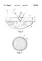
- FIG. 1is a perspective view of a solder sphere coated in accordance with the instant invention
- FIG. 2is a cross-sectional view thereof
- FIG. 3is a diagrammatical view of the reflection of light through a parylene coating
- FIG. 4is a cross-sectional view of a solder sphere coated with a flux material, and further coated with a parylene layer.
- a coated solder preform in accordance with the instant inventionis illustrated and generally indicated at 10 in FIGS. 1-2.
- a solder preform 12is coated with a layer of parylene 14 in a thickness effective to exhibit interference colors.
- Paryleneis a generic term used to describe a class of poly-p-xylylenes.
- Various forms of paryleneare commercially available for example, from Alpha Metals, Inc. Jersey City, N.J.
- the following structuresrepresent some commercially available parylene dimers. ##STR1##
- parylene for the instant inventionare those forms of parylene which melt below the melting point of the particular solder alloy used to form the solder preform.
- common tin-lead solder alloy 63Sn/37Pbhas a melting temperature of about 183° C.
- Parylene Eis a preferred form of parylene because it melts at about 180° C. While Parylene E is specifically described as the preferred embodiment in the instant example, it will be apparent to those skilled in the art that any form of parylene, including those not specifically disclosed herein, as well as combinations thereof, can be appropriately selected to correspond to the specific melting temperature of the particular solder alloy selected for the preform.
- paryleneis deposited onto the solder preforms by a vapor deposition process which is well known in the art, wherein the parylene monomer is condensed and polymerized onto the surface of the article to be coated.
- parylene dimersas illustrated above, are utilized as a starting material.
- the parylene dimeris first vaporized at a temperature of about 160° C., and then pyrolytically cleaved at a temperature of about 700° C. to form a reactive monomer vapor.
- the reactive monomer vaporis then transferred to a deposition chamber where the article to be coated is situated.
- the monomer vaporcondenses on the article surface to form a parylene polymer or co-polymer film.
- the articlesare usually placed within a rotating tumbler mounted inside the chamber.
- parylene deposition processis carried out in a closed system under negative pressure, and usually includes separate chambers for vaporization, pyrolysis, and deposition with such chambers being interconnected by a series of tubular pathways.
- the more specific details of the parylene process and deposition apparatusare well known to those skilled in the art and will not be described further.
- solder preformsare formed from solder alloys of at least two of the following metals: tin, lead, silver, bismuth, indium, antimony and cadmium.
- Tin lead alloysare typically used in concentration ranges from about 5 to about 70 weight percent tin, and about 5 to about 95 weight percent lead.
- solder preformDue to the ability of parylene to conform to various shapes, the particular shape of solder preform is not particularly critical. As stated in the background, preformed solder parts are typically no bigger than 15 mm in a major axis, and are often sub-millimeter along a minor axis, and are formed in the shapes of spheres, discs, washers, sleeves, cubes, etc., depending upon the particular manufacturing circumstances. While a solder sphere 12 is specifically disclosed as a representative example in the drawings, it is not intended to limit the scope of the claims set forth below.
- a layer of parylene 14is applied to the preformed solder sphere 12 in a thickness effective to exhibit interference colors.
- Reflective light interference in thin filmsis a well known physical phenomenon which forms the basis for the instant invention.
- FIG. 3shows an incident ray of light 16 impinging on a thin transparent film 14 of thickness t, where there is partial reflection and partial transmittance.
- Light ray 16can take two routes, AF or ABEC, and the different optical lengths of these paths leads to interference.
- nis the refractive index of the film
- tis the film thickness
- ⁇is the angle PAB.
- the geometry construct AP in FIG. 3is merely a convenient way of gaining access to the length ABEC.
- the distance AP and (EC)nare equivalent for the passage of light.
- mis an integer 1, 2, 3, 4 etc., i.e. when the waveforms are in phase, and destructive interference occurs when:
- the resultant reflected lightwill be of a few dominant wavelengths giving the characteristic strong clear colors seen for thin oil films on water, or in soap bubbles.
- the dominant wavelength(s)color
- the dominant wavelength(s)may be changed by changing the thickness of the film (t). However, beyond five to ten phases thick, there is enough randomness of phase introduced to lose a strong color effect.
- the instant phenomenonis equally applicable to solder preforms having either a spherical surface or a flat surface.
- tsuitable thickness
- iridescent colorswould be of colors close to the dominant wavelength, for example dominant blue, with violet and green iridescent colors.
- iridescenceoccurs when changing the viewing angle, which is virtually unavoidable when viewing a flat substrate with the human eye.
- the viewing angleis almost always normal to the sphere surface, and therefore a uniform color is seen.
- the refractive index of tin oxide (1.97-2.093)is higher than that of parylene (1.65).
- the generation of coloris predominantly from destructive rather than constructive interference, i.e. certain wavelengths are lost from incident white light, and a dominant color is seen from the remaining light. It is found that approximately three blue phases can be generated by coating solder spheres with parylene with the last blue phase being substantially less pure/distinctive than the first. As a dominant blue is the result of loss of yellow, then this for example, could imply a thickness of 440 nm or 0.44 ⁇ m which is the destructive thickness for yellow corresponding to the third phase thickness.
- the table belowrepresents Parylene film thicknesses versus wavelength for destructive interference:
- parylene thicknessesAs taken from the table above: 83 nm, 250 nm, 416 nm, or 583 nm. Each of the above thicknesses would provide a preform having the desired red color. Using this selection technique, it can be appreciated that a variety of different interference colors can be achieved by selecting varying thicknesses of the parylene coating.
- the minimum thickness possible to achieve an interference coloris about 50 nm, and that the maximum thickness is about 700 nm.
- the maximum thickness of about 700 nmis thought to be a reasonable maximum.
- a coated solder sphere 10further includes a coating of flux 18 on the outer surface of the solder sphere 12.
- the solder sphere coated with the flux materialwill act in virtually the same manner as the previously described solder preform.
- the flux coatingwith suitable refractive index, i.e. less than outer coating, does not significantly interfere with the appearance of interference colors as provided by the parylene coating, although colors will be more or less iridescent depending on the flux coating thickness.
- the instant inventionfurther provides an effective method of visually verifying the reflow status of a solder preform during manufacturing.
- itis often necessary to study a soldered joint to ascertain whether it has been fully soldered, i.e. heated sufficiently.
- the interference colors provided by the parylene coatingdo not persist through the reflow process.
- the colordoes not persist because the parylene coating melts at a temperature of about 180° C. and flows off of the surface of the preform, resulting in an uncoated preform after reflow. Accordingly, the change in color of the solder preform from colored to silver after reflow can be used as an effective visual check to determine if the preform has been heated sufficiently.
- Solder spheres(875 ⁇ 25 ⁇ m diameter 10Sn/90Pb alloy) used in the manufacture of Ball Grid Array packages were coated with a layer of Parylene E (4-ethyl-(2,2) paracylophane). The layer thickness was measured mechanically at 2640 ⁇ (corresponding to the second phase destructive thickness for yellow) and the color of the spheres was light blue and easily distinguishable from uncoated counterparts. An aliquot of coated and uncoated spheres were placed in glass containers and shaken for one hour. Uncoated spheres turned from silver to black and the coated (blue) spheres retained their blue color and remained substantially unaffected by the vibration.
- Both the coated and uncoated spheres in the as-received and vibrated stateswere used in the preparation of a BGA substrate with gold pads.
- a water soluble RMA flux, eutectic alloy, solder pastewas used to solder the alloy spheres to the pads on the substrate.
- the substratewas reflowed in an ATMOS 2000 belt oven with a peak temperature of 210° C. and time above 183° C. of 46 seconds.
- a nitrogen atmospherewas used providing 25 ppm of oxygen. All spheres reflowed and made good metallurgical bonds to the substrate.
- the black, uncoated vibrated spheresretained their black color after reflow. However, the "blue" parylene coated spheres (vibrated and as-received) had returned to a bright gloss silver appearance after reflow.
- the instant inventionprovides an effective coating for physically protecting solder preforms from the rigors of handling and manufacturing, protecting the solder preforms from atmospheric conditions, and for providing a unique optical characteristic to distinguish one type of preforms from another. Furthermore, since the interference colors do not persist through the reflow process, the color coating provide a unique means of verifying the reflow status of the sphere by examining the preform for loss of color after reflow. For these reasons, the instant invention is believed to represent a significant advancement in the art which has substantial commercial merit.
Landscapes
- Engineering & Computer Science (AREA)
- Mechanical Engineering (AREA)
- Manufacturing & Machinery (AREA)
- Microelectronics & Electronic Packaging (AREA)
- Adornments (AREA)
- Spectrometry And Color Measurement (AREA)
Abstract
Description
2tn cos φ
2tn cos φ+λ/2
2tn cos φ+λ/2=mλ
2tn cos φ+λ/2=(m+1/2)λ
2tn cos φ=mλ
2tn cos φ+λ/2=mλ
______________________________________ Phase 1 2 3 4 5 6 WAVELENGTH λ/2 3λ/2 5λ/2 7λ/2 9λ/2 11λ/2 ______________________________________ λviolet 400 nm 60 180 300 420 540 660 λblue 440 nm 66 200 333 467 600 733 λgreen 550 nm 83 250 416 583 750 916 λyellow 580 nm 88 264 440 615 791 967 λred 660 nm 100 300 500 700 900 1100 (parylene film thickness in (nm) for destrictive interference ______________________________________
Claims (40)
Priority Applications (3)
| Application Number | Priority Date | Filing Date | Title |
|---|---|---|---|
| US08/498,247US5789068A (en) | 1995-06-29 | 1995-06-29 | Preformed solder parts coated with parylene in a thickness effective to exhibit predetermined interference colors |
| PCT/US1996/011012WO1997001414A1 (en) | 1995-06-29 | 1996-06-28 | Preformed solder parts coated with parylene in a thickness effective to exhibit predetermined interference colors |
| AU63419/96AAU6341996A (en) | 1995-06-29 | 1996-06-28 | Preformed solder parts coated with parylene in a thickness effective to exhibit predetermined interference colors |
Applications Claiming Priority (1)
| Application Number | Priority Date | Filing Date | Title |
|---|---|---|---|
| US08/498,247US5789068A (en) | 1995-06-29 | 1995-06-29 | Preformed solder parts coated with parylene in a thickness effective to exhibit predetermined interference colors |
Publications (1)
| Publication Number | Publication Date |
|---|---|
| US5789068Atrue US5789068A (en) | 1998-08-04 |
Family
ID=23980225
Family Applications (1)
| Application Number | Title | Priority Date | Filing Date |
|---|---|---|---|
| US08/498,247Expired - LifetimeUS5789068A (en) | 1995-06-29 | 1995-06-29 | Preformed solder parts coated with parylene in a thickness effective to exhibit predetermined interference colors |
Country Status (3)
| Country | Link |
|---|---|
| US (1) | US5789068A (en) |
| AU (1) | AU6341996A (en) |
| WO (1) | WO1997001414A1 (en) |
Cited By (23)
| Publication number | Priority date | Publication date | Assignee | Title |
|---|---|---|---|---|
| US5984161A (en)* | 1996-12-10 | 1999-11-16 | Degussa-Huls Aktiengesellschaft | Flux-encased resilient solder preforms and process for the preparation thereof |
| US6052045A (en)* | 1999-03-12 | 2000-04-18 | Kearney-National, Inc. | Electromechanical switching device package with controlled impedance environment |
| US6068176A (en)* | 1997-12-29 | 2000-05-30 | Vitta Corporation | Brazing alloy transfer tape having a visually distinctive carrier |
| JP2000288771A (en)* | 1999-04-09 | 2000-10-17 | Senju Metal Ind Co Ltd | Solder ball and coating method on solder ball |
| US20020141384A1 (en)* | 2001-03-28 | 2002-10-03 | Fu-Hua Liu | System and method for determining a connectionless communication path for communicating audio data through an address and port translation device |
| US20030003356A1 (en)* | 2000-02-02 | 2003-01-02 | Quallion Llc | Bipolar electronics package |
| US6545809B1 (en)* | 1999-10-20 | 2003-04-08 | Flex Products, Inc. | Color shifting carbon-containing interference pigments |
| US20030169138A1 (en)* | 2002-03-08 | 2003-09-11 | Motta James J. | Surface mount molded relay package and method of manufacturing same |
| US20030211388A1 (en)* | 2000-04-26 | 2003-11-13 | Alan Ruth | Battery |
| US20030211386A1 (en)* | 2000-02-02 | 2003-11-13 | Ruth Douglas Alan | Sealed battery and case therefor |
| USRE38381E1 (en) | 2000-07-21 | 2004-01-13 | Kearney-National Inc. | Inverted board mounted electromechanical device |
| US20050196949A1 (en)* | 2004-03-08 | 2005-09-08 | Hitachi Metals, Ltd. | Solder ball excellent in micro-adhesion preventing properties and wetting properties and method for preventing the micro-adhesion of solder balls |
| US20060083770A1 (en)* | 2004-10-15 | 2006-04-20 | Specialty Coating Systems, Inc. | Medical devices and methods of preparation and use |
| US7166388B2 (en) | 2000-02-02 | 2007-01-23 | Quallion Llc | Brazed ceramic seal for batteries |
| US20070148390A1 (en)* | 2005-12-27 | 2007-06-28 | Specialty Coating Systems, Inc. | Fluorinated coatings |
| US20090186998A1 (en)* | 2005-10-31 | 2009-07-23 | Specialty Coating Systems, Inc. | Parylene variants and methods of synthesis and use |
| US20090285987A1 (en)* | 2007-02-26 | 2009-11-19 | Speciality Coating Systems, Inc. | Perfluoroparacyclophane and related methods therefor |
| US20190118308A1 (en)* | 2011-09-23 | 2019-04-25 | Lucas-Milhaupt | Luminescent Braze Preforms |
| CN109881178A (en)* | 2019-04-19 | 2019-06-14 | 江苏可润光电科技有限公司 | A kind of Parylene colour coating process and coating apparatus |
| CN113579554A (en)* | 2021-08-13 | 2021-11-02 | 深圳市福摩索金属制品有限公司 | High-performance preformed soldering lug and welding method thereof |
| JP2021180705A (en)* | 2020-05-18 | 2021-11-25 | 株式会社モリタ製作所 | Coated article |
| US11602808B2 (en)* | 2019-04-30 | 2023-03-14 | Indium Corporation | Solder preform with internal flux core including thermochromic indicator |
| US12034092B2 (en)* | 2015-09-25 | 2024-07-09 | Materion Corporation | High optical power light conversion device using a phosphor element with solder attachment |
Families Citing this family (5)
| Publication number | Priority date | Publication date | Assignee | Title |
|---|---|---|---|---|
| TW418148B (en)* | 1997-11-11 | 2001-01-11 | Kobe Steel Ltd | Wire for welding |
| JP2004500700A (en)* | 1999-06-01 | 2004-01-08 | アルファ・メタルズ・インコーポレーテッド | Method for protective coating of BGA solder alloy balls |
| US6506448B1 (en)* | 1999-06-01 | 2003-01-14 | Fry's Metals, Inc. | Method of protective coating BGA solder alloy spheres |
| DE10030310A1 (en) | 2000-06-27 | 2002-01-10 | Buerkle Gmbh Robert | Application device for applying liquids to plate-shaped workpieces |
| DE10030316A1 (en) | 2000-06-27 | 2002-01-10 | Buerkle Gmbh Robert | Application device for applying liquids to plate-shaped workpieces |
Citations (11)
| Publication number | Priority date | Publication date | Assignee | Title |
|---|---|---|---|---|
| US3300332A (en)* | 1966-02-07 | 1967-01-24 | Union Carbide Corp | Coated particulate material and method for producing same |
| GB2027617A (en)* | 1978-08-01 | 1980-02-27 | Johnson Matthey Co Ltd | Flux coated brazing materials |
| US4225647A (en)* | 1977-12-02 | 1980-09-30 | Parent Richard A | Articles having thin, continuous, impervious coatings |
| US4298407A (en)* | 1980-08-04 | 1981-11-03 | E. I. Du Pont De Nemours And Company | Flux treated solder powder composition |
| US4380518A (en)* | 1982-01-04 | 1983-04-19 | Western Electric Company, Inc. | Method of producing solder spheres |
| US4758288A (en)* | 1987-06-08 | 1988-07-19 | Ronald T. Dodge Co. | Encapsulated lithium granules and method of manufacture |
| US4994326A (en)* | 1987-10-27 | 1991-02-19 | Tamura Kaken Co., Ltd. | Solder powders coated with fluorine compounds, and solder pastes |
| EP0448016A1 (en)* | 1990-03-19 | 1991-09-25 | Union Carbide Chemicals And Plastics Company, Inc. | Process for optimizing corrosion protection of coated substrates |
| US5069972A (en)* | 1988-09-12 | 1991-12-03 | Versic Ronald J | Moldable microcapsule that contains a high percentage of solid core material, and method of manufacture thereof |
| EP0556864A1 (en)* | 1992-02-21 | 1993-08-25 | London Chemical Company, Inc. | Solder powder coated with parylene |
| EP0766811A1 (en)* | 1994-06-24 | 1997-04-09 | Shields Enterprises, Inc. | Electronic navigation system and method |
Family Cites Families (1)
| Publication number | Priority date | Publication date | Assignee | Title |
|---|---|---|---|---|
| US4505421A (en)* | 1981-10-05 | 1985-03-19 | Raychem Corporation | Soldering methods and devices |
- 1995
- 1995-06-29USUS08/498,247patent/US5789068A/ennot_activeExpired - Lifetime
- 1996
- 1996-06-28AUAU63419/96Apatent/AU6341996A/ennot_activeAbandoned
- 1996-06-28WOPCT/US1996/011012patent/WO1997001414A1/enactiveApplication Filing
Patent Citations (14)
| Publication number | Priority date | Publication date | Assignee | Title |
|---|---|---|---|---|
| US3300332A (en)* | 1966-02-07 | 1967-01-24 | Union Carbide Corp | Coated particulate material and method for producing same |
| US4225647B1 (en)* | 1977-12-02 | 1995-05-09 | Richard A Parent | Articles having thin, continuous, impervious coatings |
| US4225647A (en)* | 1977-12-02 | 1980-09-30 | Parent Richard A | Articles having thin, continuous, impervious coatings |
| GB2027617A (en)* | 1978-08-01 | 1980-02-27 | Johnson Matthey Co Ltd | Flux coated brazing materials |
| US4298407A (en)* | 1980-08-04 | 1981-11-03 | E. I. Du Pont De Nemours And Company | Flux treated solder powder composition |
| US4380518A (en)* | 1982-01-04 | 1983-04-19 | Western Electric Company, Inc. | Method of producing solder spheres |
| US4758288A (en)* | 1987-06-08 | 1988-07-19 | Ronald T. Dodge Co. | Encapsulated lithium granules and method of manufacture |
| US4994326A (en)* | 1987-10-27 | 1991-02-19 | Tamura Kaken Co., Ltd. | Solder powders coated with fluorine compounds, and solder pastes |
| US5069972A (en)* | 1988-09-12 | 1991-12-03 | Versic Ronald J | Moldable microcapsule that contains a high percentage of solid core material, and method of manufacture thereof |
| EP0448016A1 (en)* | 1990-03-19 | 1991-09-25 | Union Carbide Chemicals And Plastics Company, Inc. | Process for optimizing corrosion protection of coated substrates |
| EP0556864A1 (en)* | 1992-02-21 | 1993-08-25 | London Chemical Company, Inc. | Solder powder coated with parylene |
| US5272007A (en)* | 1992-02-21 | 1993-12-21 | Union Carbide Chemicals & Plastics Technology Corporation | Solder powder coated with parylene |
| US5328522A (en)* | 1992-02-21 | 1994-07-12 | Union Carbide Chemicals & Plastics Technology Corporation | Solder pastes |
| EP0766811A1 (en)* | 1994-06-24 | 1997-04-09 | Shields Enterprises, Inc. | Electronic navigation system and method |
Cited By (42)
| Publication number | Priority date | Publication date | Assignee | Title |
|---|---|---|---|---|
| US5984161A (en)* | 1996-12-10 | 1999-11-16 | Degussa-Huls Aktiengesellschaft | Flux-encased resilient solder preforms and process for the preparation thereof |
| US6068176A (en)* | 1997-12-29 | 2000-05-30 | Vitta Corporation | Brazing alloy transfer tape having a visually distinctive carrier |
| US6052045A (en)* | 1999-03-12 | 2000-04-18 | Kearney-National, Inc. | Electromechanical switching device package with controlled impedance environment |
| JP2000288771A (en)* | 1999-04-09 | 2000-10-17 | Senju Metal Ind Co Ltd | Solder ball and coating method on solder ball |
| USRE45537E1 (en) | 1999-04-09 | 2015-06-02 | Senju Metal Industry Co., Ltd. | Coated solder spheres and method for producing the same |
| JP3503523B2 (en) | 1999-04-09 | 2004-03-08 | 千住金属工業株式会社 | Solder ball and solder ball coating method |
| US20040165272A1 (en)* | 1999-10-20 | 2004-08-26 | Phillips Roger W. | Color shifting carbon-containing interference pigments |
| US6751022B2 (en) | 1999-10-20 | 2004-06-15 | Flex Products, Inc. | Color shifting carbon-containing interference pigments and foils |
| US6833959B2 (en) | 1999-10-20 | 2004-12-21 | Flex Products, Inc. | Color shifting carbon-containing interference pigments |
| US6831785B2 (en) | 1999-10-20 | 2004-12-14 | Flex Products, Inc. | Color shifting carbon-containing interference pigments |
| US6545809B1 (en)* | 1999-10-20 | 2003-04-08 | Flex Products, Inc. | Color shifting carbon-containing interference pigments |
| US20040160672A1 (en)* | 1999-10-20 | 2004-08-19 | Phillips Roger W. | Color shifting carbon-containing interference pigments |
| US6744559B2 (en) | 1999-10-20 | 2004-06-01 | Flex Products, Inc. | Color shifting carbon-containing interference pigments and foils |
| US7410512B2 (en) | 2000-02-02 | 2008-08-12 | Quallion Llc | Bipolar electronics package |
| US20030003356A1 (en)* | 2000-02-02 | 2003-01-02 | Quallion Llc | Bipolar electronics package |
| US7166388B2 (en) | 2000-02-02 | 2007-01-23 | Quallion Llc | Brazed ceramic seal for batteries |
| US20030211386A1 (en)* | 2000-02-02 | 2003-11-13 | Ruth Douglas Alan | Sealed battery and case therefor |
| US7175938B2 (en) | 2000-02-02 | 2007-02-13 | Quallion Llc | Battery case employing ring sandwich |
| US7041413B2 (en) | 2000-02-02 | 2006-05-09 | Quallion Llc | Bipolar electronics package |
| US20060156538A1 (en)* | 2000-02-02 | 2006-07-20 | Hisashi Tsukamoto | Bipolar electronics package |
| US20030211388A1 (en)* | 2000-04-26 | 2003-11-13 | Alan Ruth | Battery |
| US7285355B2 (en) | 2000-04-26 | 2007-10-23 | Quallion Llc | Battery |
| USRE38381E1 (en) | 2000-07-21 | 2004-01-13 | Kearney-National Inc. | Inverted board mounted electromechanical device |
| US20020141384A1 (en)* | 2001-03-28 | 2002-10-03 | Fu-Hua Liu | System and method for determining a connectionless communication path for communicating audio data through an address and port translation device |
| US20030169138A1 (en)* | 2002-03-08 | 2003-09-11 | Motta James J. | Surface mount molded relay package and method of manufacturing same |
| US7198983B2 (en) | 2004-03-08 | 2007-04-03 | Hitachi Metals, Ltd. | Solder ball excellent in micro-adhesion preventing properties and wetting properties and method for preventing the micro-adhesion of solder balls |
| US20050196949A1 (en)* | 2004-03-08 | 2005-09-08 | Hitachi Metals, Ltd. | Solder ball excellent in micro-adhesion preventing properties and wetting properties and method for preventing the micro-adhesion of solder balls |
| US20060083770A1 (en)* | 2004-10-15 | 2006-04-20 | Specialty Coating Systems, Inc. | Medical devices and methods of preparation and use |
| US20090186998A1 (en)* | 2005-10-31 | 2009-07-23 | Specialty Coating Systems, Inc. | Parylene variants and methods of synthesis and use |
| US7994372B2 (en) | 2005-10-31 | 2011-08-09 | Specialty Coating Systems, Inc. | Parylene variants and methods of synthesis and use |
| US20070148390A1 (en)* | 2005-12-27 | 2007-06-28 | Specialty Coating Systems, Inc. | Fluorinated coatings |
| US20100260934A9 (en)* | 2007-02-26 | 2010-10-14 | Speciality Coating Systems, Inc. | Perfluoroparacyclophane and related methods therefor |
| US7652178B2 (en) | 2007-02-26 | 2010-01-26 | Specialty Coating Systems, Inc. | Perfluoroparacyclophane and methods of synthesis and use thereof |
| US20090285987A1 (en)* | 2007-02-26 | 2009-11-19 | Speciality Coating Systems, Inc. | Perfluoroparacyclophane and related methods therefor |
| US20190118308A1 (en)* | 2011-09-23 | 2019-04-25 | Lucas-Milhaupt | Luminescent Braze Preforms |
| US10987763B2 (en)* | 2011-09-23 | 2021-04-27 | Lucas-Milhaupt, Inc. | Luminescent braze preforms |
| US12034092B2 (en)* | 2015-09-25 | 2024-07-09 | Materion Corporation | High optical power light conversion device using a phosphor element with solder attachment |
| CN109881178A (en)* | 2019-04-19 | 2019-06-14 | 江苏可润光电科技有限公司 | A kind of Parylene colour coating process and coating apparatus |
| US11602808B2 (en)* | 2019-04-30 | 2023-03-14 | Indium Corporation | Solder preform with internal flux core including thermochromic indicator |
| US20230191541A1 (en)* | 2019-04-30 | 2023-06-22 | Indium Corporation | Solder preform with internal flux core including thermochromic indicator |
| JP2021180705A (en)* | 2020-05-18 | 2021-11-25 | 株式会社モリタ製作所 | Coated article |
| CN113579554A (en)* | 2021-08-13 | 2021-11-02 | 深圳市福摩索金属制品有限公司 | High-performance preformed soldering lug and welding method thereof |
Also Published As
| Publication number | Publication date |
|---|---|
| WO1997001414A1 (en) | 1997-01-16 |
| AU6341996A (en) | 1997-01-30 |
Similar Documents
| Publication | Publication Date | Title |
|---|---|---|
| US5789068A (en) | Preformed solder parts coated with parylene in a thickness effective to exhibit predetermined interference colors | |
| CA1253367A (en) | Thin film optical variable article having substantial color shift with angle and method | |
| US4953922A (en) | Web material for camouflage against electromagnetic radiation | |
| CA1322637C (en) | Method for preparing light polarizer | |
| DK166864B1 (en) | PASTEURIZABLE HEAT PREPARATION SHRINKLE WRAPLE AND PROCEDURE FOR PREPARING THE WRAP | |
| US4034375A (en) | Laminated camouflage material | |
| JPS5627106A (en) | Beam splitter | |
| JPS6036355A (en) | Manufacture of plate with permeability of 5-40 percents in visible spectrum zone and reflectivity against heat ray | |
| WO1998001779A1 (en) | Multilayer film with differential retroreflectivity | |
| JP2011508265A (en) | Retroreflective article and retroreflective element comprising a spherical core and two concentric optical interference layers | |
| SE459695B (en) | CAMO FLAG MATERIAL WITH SEMI-CONDUCTIVE LAYERS AND PROCEDURES FOR PREPARING THE CAMO FLAG MATERIAL | |
| Carniglia et al. | Recent damage results on silica/titania reflectors at 1 micron | |
| CA2021917A1 (en) | Non-melting microwave susceptor films | |
| JPS62258415A (en) | Optical filter | |
| JP2006518316A (en) | Heat-sealed and sterilized product packaging, packaging material therefor and use of the packaging material | |
| CA2020612A1 (en) | Tape coating | |
| BR9504449A (en) | Film subject to thermal contraction of multiple layers | |
| BRPI0820392B1 (en) | multilayer embossed film | |
| JP2003177224A (en) | Encapsulated-lens retroreflective sheet and method for manufacturing the same | |
| JPH0411002B2 (en) | ||
| CN114746602A (en) | Multilayer multifunctional thermal management material | |
| JPH0529076A (en) | Low temperature susceptor | |
| JP2020196536A (en) | Packaging material, packaging container, and lid body | |
| JP2014051328A (en) | Packaging material | |
| US5728455A (en) | Randomly patterned cookware |
Legal Events
| Date | Code | Title | Description |
|---|---|---|---|
| AS | Assignment | Owner name:FRY'S METALS INC., A DE CORP., NEW JERSEY Free format text:ASSIGNMENT OF ASSIGNORS INTEREST;ASSIGNORS:KING, CHARLES E.;GULINO, ANGELO J.;REEL/FRAME:007605/0733 Effective date:19950627 | |
| STCF | Information on status: patent grant | Free format text:PATENTED CASE | |
| FPAY | Fee payment | Year of fee payment:4 | |
| AS | Assignment | Owner name:SPECIALTY COATING SYSTEMS, INC., INDIANA Free format text:ASSIGNMENT OF ASSIGNORS INTEREST;ASSIGNOR:ALPHA METALS, INC.;REEL/FRAME:017388/0222 Effective date:20051214 | |
| FPAY | Fee payment | Year of fee payment:8 | |
| AS | Assignment | Owner name:ROYNAT BUSINESS CAPITAL INC., AS AGENT, NORTH CARO Free format text:NOTICE OF GRANT OF SECURITY INTEREST;ASSIGNOR:SPECIALTY COATING SYSTEMS, INC.;REEL/FRAME:017519/0063 Effective date:20051230 | |
| AS | Assignment | Owner name:SPECIALTY COATING SYSTEMS, INC., INDIANA Free format text:ASSIGNMENT OF ASSIGNORS INTEREST;ASSIGNOR:FRY'S METALS, INC.;REEL/FRAME:018535/0453 Effective date:20051214 | |
| AS | Assignment | Owner name:SPECIALTY COATING SYSTEMS, INC., INDIANA Free format text:RELEASE BY SECURED PARTY;ASSIGNOR:ROYNAT BUSINESS CAPITAL, INC.;REEL/FRAME:021109/0835 Effective date:20080610 | |
| FPAY | Fee payment | Year of fee payment:12 |