US5787042A - Method and apparatus for reading out a programmable resistor memory - Google Patents
Method and apparatus for reading out a programmable resistor memoryDownload PDFInfo
- Publication number
- US5787042A US5787042AUS08/819,991US81999197AUS5787042AUS 5787042 AUS5787042 AUS 5787042AUS 81999197 AUS81999197 AUS 81999197AUS 5787042 AUS5787042 AUS 5787042A
- Authority
- US
- United States
- Prior art keywords
- signal
- readout
- circuit
- node
- threshold level
- Prior art date
- Legal status (The legal status is an assumption and is not a legal conclusion. Google has not performed a legal analysis and makes no representation as to the accuracy of the status listed.)
- Expired - Lifetime
Links
Images


Classifications
- G—PHYSICS
- G11—INFORMATION STORAGE
- G11C—STATIC STORES
- G11C13/00—Digital stores characterised by the use of storage elements not covered by groups G11C11/00, G11C23/00, or G11C25/00
- G11C13/0002—Digital stores characterised by the use of storage elements not covered by groups G11C11/00, G11C23/00, or G11C25/00 using resistive RAM [RRAM] elements
- G11C13/0004—Digital stores characterised by the use of storage elements not covered by groups G11C11/00, G11C23/00, or G11C25/00 using resistive RAM [RRAM] elements comprising amorphous/crystalline phase transition cells
- G—PHYSICS
- G11—INFORMATION STORAGE
- G11C—STATIC STORES
- G11C13/00—Digital stores characterised by the use of storage elements not covered by groups G11C11/00, G11C23/00, or G11C25/00
- G11C13/0002—Digital stores characterised by the use of storage elements not covered by groups G11C11/00, G11C23/00, or G11C25/00 using resistive RAM [RRAM] elements
- G11C13/0021—Auxiliary circuits
- G11C13/004—Reading or sensing circuits or methods
- G—PHYSICS
- G11—INFORMATION STORAGE
- G11C—STATIC STORES
- G11C7/00—Arrangements for writing information into, or reading information out from, a digital store
- G11C7/06—Sense amplifiers; Associated circuits, e.g. timing or triggering circuits
Definitions
- the present inventionrelates to the comparison circuitry in a memory device.
- the inventionis directed to an automatic firing circuit to read a memory cell 3and automatic protecting circuit to connect and isolate the comparison circuitry from an array of programmable memory cells.
- DRAM integrated circuit arrayshave existed for more than twenty five years and have evolved from the earliest one kilobit (Kb) generation to the recent 256 megabit (Mb) generation. This dramatic increase in storage capacity has been achieved through advances in semiconductor fabrication technology and circuit design technology. The tremendous advances in these two technologies have also achieved higher and higher levels of integration that permit dramatic reductions in memory array size and cost, as well as increased process yield.
- a DRAM memory celltypically comprises, as basic components, an access transistor (switch) and a capacitor for storing a binary data bit in the form of a charge.
- an access transistorswitch
- a capacitorfor storing a binary data bit in the form of a charge.
- a charge of one polarityis stored on the capacitor to represent a binary "1”
- a stored charge of the opposite polarityrepresents a binary "0”.
- the basic drawback of a DRAMis that the charge on the capacitor eventually leaks away, and therefore provisions must be made to "refresh" the capacitor charge or else the data bit stored by the memory cell is lost.
- the memory cell of a conventional SRAMcomprises, as basic components, an access transistor or transistors and a memory element in the form of two or more integrated circuit devices interconnected to function as a bistable latch.
- An example of a bistable latchis cross-coupled inverters. Bistable latches do not need to be "refreshed", as in the case of DRAM memory cells, and will reliably store a data bit indefinitely as long as they continue to receive supply voltage.
- a programmable resistance element of such materialcould be programmed (set) to a high resistive state to store, for example, a binary "1" data bit or programmed to a low resistive state to store, for example, a binary "0" data bit.
- the stored data bitcould then be retrieved by detecting either the magnitude of a voltage drop over or the magnitude of a current flowing through the resistive memory element by readout circuitry, thus indicating its stable resistance state.
- chalcogenidesuch as, for example, the alloy Ge:Sb:Te disclosed in Ovshinsky et al., U.S. Pat. No. 5,414,271, the disclosure of which is incorporated herein by reference.
- a memory element comprised of a chalcogenide materialcan be programmed to a stable high resistive state by passing a narrow, high amplitude current pulse through it.
- a lower amplitude current pulse of longer durationprograms a chalcogenide memory element to a stable, low resistive state.
- the appropriate current pulsereprograms the chalcogenide memory element, relieving the need to first erase the memory cell.
- a memory element of chalcogenide materialis nonvolatile, in that it retains its programmed resistive state regardless of whether it is connected to a power supply.
- circuitry for reading out a data bit stored in a memory cell of a memory arraycomprising a readout circuit including at least one sense node coupled to receive a readout signal from the memory cell; and a detector circuit coupled to the sense node and operating when the readout signal achieves a threshold level indicative of the data bit stored in the memory cell to condition the readout circuit such that the sense node is driven to a logic signal level that reliably indicates a binary value of the stored data bit.
- a method of reading out a data bit stored by a programmable resistor memory elementcomprising the steps of coupling a first sense node to receive a readout signal from the memory element during a readout cycle; coupling a second sense node to receive a reference signal; detecting the readout signal developing on the first sense node; detecting the reference signal developing on the second sense node; generating a trigger signal when one of the developing readout and reference signals achieves a threshold; and driving the first and second sense nodes, in response to the trigger signal, to opposite logic signal levels indicative of a binary value of the stored data bit.
- FIG. 1is a functional block diagram of typical read/write circuitry serving a SRAM memory cell array of resistive memory elements
- FIG. 2is a schematic diagram of circuitry that has been proposed for reading data bits stored in the SRAM memory cell array of FIG. 1;
- FIG. 3is a schematic diagram of readout circuitry in accordance with a preferred embodiment of the present invention.
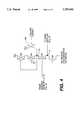
- FIG. 4is a detailed schematic diagram of one of a pair of detectors included in the readout circuitry of FIG. 3;
- FIG. 5ais a timing diagram illustrating the operation of readout circuitry in FIG. 3 when reading out a binary "1";
- FIG. 5bis a timing diagram illustrating the operation of the readout circuitry of FIG. 3 when reading out a binary "0".
- a problem indigenous to existing chalcogenide resistance element memoriesis that the readout (comparison) circuitry requires high voltages to drive comparators to states capable of reliably outputting to other computer components data bits stored in the memory. These high voltages are capable of spuriously reprogramming the memory elements, causing data corruption.
- existing technologyhas imposed artificially long time delays in the read out cycles. This artificial time delay provides a safety margin to accommodate variations in readout circuitry characteristics.
- Two such safety margins effecting circuit response timeare manufacturing imperfections and operating conditions. Circuit response time depends on tolerances in the manufacturing process which cause imperfections in batches of manufactured circuits. In other words, two batches of readout circuits will normally require different times to sense the resistive state of a memory element.
- the readout circuitrywould be classified as slow or fast. Response time is also influenced by whether the operating conditions of the circuit are optimal or suboptimal. Thus, when building the artificial time delay into a readout cycle, the manufacturer must include a sufficient time delay to ensure that the slowest batch of integrated circuits, operating under the worst (most suboptimal) conditions, will sensed the resistive state of the memory element prior to supplying high voltages to drive the comparator into a state accurately registering the binary value of the stored data bit.
- the present inventionovercomes this problem by monitoring the comparator to detect when it receives a readout signal from the memory cell of sufficient magnitude to reliably indicate that it has read out the resistive state of the memory element, which is, indicative of the binary value of the stored data bit. At that moment, the readout circuitry isolates the comparator from the memory cell to prevent reprogramming the memory cell as the high voltage is applied to the comparator. Thus, the readout cycle time is tailored to each comparison circuit, regardless of the manufacturing tolerance or operating conditions.
- FIG. 1illustrates a memory system 100 separated into basic functional blocks.
- a programmable memory 102contains an array of memory cells, each including a resistor formed of a material, such as, for example, chalcogenide, whose resistive state can be programmed to either a high or low ohmic value by subjection to electrical impulses.
- a column decoder 104receives a column address signal for selecting a particular column of memory 102, and row decoder 106 receives a row address signal for selecting a particular row. A data bit can then be written into or read from the addressed memory cell located at the intersection of the selected row and column.
- Write circuit 108operates to program individual memory cells in memory 102. Specifically, write circuit 108 receives a write data signal to program the memory cell addressed by the column and row decoders. Write circuit 108 then drives an appropriate constant current through the resistive element of the addressed memory cell, causing it to exhibit either a stable high resistance state indicating storage of, for example, a binary "1", or a stable low resistance state indicating storage of, for example, a binary "0".
- comparison circuit 110operates to supply a regulated current to a both a reference resistor (not shown) and an addressed memory cell in memory 102. Based upon whether the voltage drop across the memory cell is higher or lower than the voltage drop across the reference resistor, comparison circuit 110 outputs a binary "1” or a binary "0" logic signal indicative of the data bit stored in the memory cell.
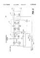
- FIG. 2illustrates a comparison circuit according to the disclosure in Morgan.
- comparison circuit 200compares the voltage drop across a reference resistor (not shown) connected to an input line 202 to a voltage drop across a memory cell (not shown) connected to input line 204.
- These input linesare separately connected through isolation transistors 206a and 206b of an isolation circuit 14 to a helper flip-flop 12 (comparator).
- Helper flip-flop 12includes two CMOS inverters, i.e., an n-channel MOS transistor 208 and a p-channel MOS transistor 212, cross-coupled to an n-channel MOS transistor 210 and a p-channel MOS transistor 214. These inverters are connected to sense nodes FF1 and FF2 of helper flip-flop 12, to which input lines 202 and 204 are respectively connected during a readout cycle.
- a COLUMN ENABLE signalis low, signifying that comparison circuit 200 is disconnected from the memory cell array and sense nodes FF1 and FF2 are shorted together to equalize their potentials at a low precharge level, as described in Morgan.
- Fire helper flip-flop (FHFF) signalis also low at this time, which maintains transistor 226 off, thus disconnecting the sources of transistors 208 and 210 from ground.
- the low FHFF signalturns transistor 228 off via inverter 230, thereby disconnecting the sources of transistors 212 and 214 from source voltage Vcc.
- a READ signalis preferably low, which, when inverted by inverter 236 and NORed with the low FHFF signal, isolates input lines 202 and 204 from nodes FF1 and FF2, respectively, by turning off isolation transistors 206a and 206b via inverter 236 and NOR gate 234. Also, a READ -- REG signal is isolated from helper flip-flop 12 by the off state of transistors 222 and 224 imposed by the output of NOR gate 234, as applied through inverter 232.
- COLUMN ENABLEgoes high to turn off transistors 218 and 220, such that sense nodes FF1 and FF2 are no longer shorted together. Additionally, the READ signal goes high, which, when NORed with the low FHFF signal, causes the output of NOR gate 234 to go high.
- the high NOR gate 234 outputturns an isolation transistors 206a and 206b, connecting input lines 202 and 204 to helper flip-flop 12. Additionally, the high output from NOR gate 234 turns on transistors 222 and 224, supplying READ -- REG voltage to nodes FF1 and FF2.
- a readout currentflows through input line 204 and the programed resistive element of the addressed memory cell.
- a reference currentflows through input line 202 and the connected reference resistor.
- the nodes FF1 and FF2then assume potentials as determined by the voltage drops developed across the reference resistor and the programmed resistive element of the addressed memory cell preparatory to setting a latched state of helper flip-flop 12.
- the relationship of the FF2 node potential to the FF1 node potentialis indicative of whether the addressed memory cell resistance has been programmed to a high resistance, e.g., a binary "1", or a low resistance, e.g., a binary "0".
- FHFF signalgoes high and, when NORed with the inverted READ signal, which is a low signal, turns off isolation transistors 206a and 206b via NOR gate 234.
- Input lines 202 and 204are then isolated from nodes FF1 and FF2, and transistors 222 and 224 are turned off via NOR gate 234 and inverter 232 to remove READ -- REG from nodes FF1 and FF2.
- FHFFturns on transistors 226 and 228 to connect the sources of transistors 208 and 212 to ground and the sources of transistors 210 and 214 to Vcc, thereby "firing" helper flip-flop 12.
- one of the nodes FF1, FF2is driven to Vcc and the other of the nodes FF1, FF2 is driven to ground as helper flip-flop 12 is "fired”.
- the latched logic level potentials Vcc and ground on nodes FF1 and FF2are read out through gating circuitry shown in Morgan to indicate whether a binary "1" or a binary "0" has been read from the addressed memory cell.
- Comparison circuit 200reliably reads data stored in a programmable resistor memory; however, an artificial time delay is necessary to ensure that the potentials on sense nodes FF1 and FF2 have achieve levels reliably indicative of the resistive state of the addressed memory cell of memory 102 before helper flip-flop 12 is isolated from the memory cell and fired.
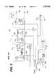
- comparison circuit 300seen in FIG. 3, overcomes this drawback of comparison circuit 200, in FIG. 2, by eliminating the need for an artificial long time delay that, in most cases, is unnecessary.
- comparison circuit 300includes a detector 24 that operates to generate a trip signal. The trip signal indicates that helper flip-flop 12 has reliably read out the resistive state of the memory cell and initiates firing of helper flip-flop 12.
- this trip signaladvantageously serves the purpose of the FHFF signal in comparison circuit 200, of FIG. 2, but without the artificial time delay.
- a detector circuit 24includes detector circuits 18 and 20, and a NAND gate 301.
- a trip signal issued by either one of detectors 18 or 20passes through NAND gate 301 to set a latch 22 consisting of cross-connected NOR gates 302 and 304.
- the set output appearing at the output of NOR gate 304then serves as an FHFF trigger signal to fire helper flip-flop 12 in circuit 300 in the same manner as comparison circuit 200 of FIG. 2.
- the operation of the detectorsis explained below.
- detector 18includes a string of four transistors connected in series between Vcc and ground. Specifically, the source of a p-channel transistor 18a is connected to Vcc and its drain is connected through the source-drain circuits of p-channel transistors 18b and 18c and n-channel transistor 18d to ground. The gates of transistors 18c and 18d are connected in common to helper flip-flop node FF1, and a node A between the transistor 18c drain and transistor 18d drain is connected to one input of NAND gate 301 in FIG. 3.
- a p-channel transistor 18ehas its source connected to Vcc, its drain connected to the junction 19 of the transistor 18b drain and transistor 18c source, and its gate connected to receive the COLUMN ENABLE signal.
- the gate of transistor 18ais connected to junction 19, and the gate of transistor 18b is grounded.
- the COLUMN ENABLE signalis low, and thus transistor 18e is turned on to apply Vcc to junction 19, which, in turn, maintains transistor 18a off.
- COLUMN ENABLEis thus high to turn on transistors 218 and 220, which, as seen in FIG. 3, connects nodes FF1 and FF2 to a common, low precharge potential.
- transistor 18cis turned on and transistor 18d is turned off, and output node A assumes a high potential approximating Vcc.
- the same conditionsprevail in detector circuit 20, and thus its output node B is also high.
- the COLUMN ENABLE and READ signalsgo high.
- the COLUMN ENABLE signalgoes low.
- the detector outputs A and Bremain high, the output of NOR gate 304 remains low to maintain transistors 226 and 228 off.
- helper flip-flop 12remains disconnected from Vcc and ground. Since the two inputs to NOR gate 234, i.e., the READ signal inverted by inverter 236 and the output of NOR gate 304, are low, the output of NOR gate 234 goes high at To to turn on transistors 222 and 224 via inverter 232, as well as isolation transistors 206a and 206b.
- the low COLUMN ENABLE signalturns off transistors 218 and 220, such that the READ -- REG current applied through transistors 222 and 224, begins charging nodes FF1 and FF2 in accordance with the currents respectively flowing through a reference resistor 203 connected to input line 202 and through the resistor element 205 of the addressed memory cell connected to input line 204 (FIG. 3).
- output nodes A and B of detectors 18 and 20are high, i.e., approximately equal to the reference voltage Vr on nodes 19.
- currentsbegin flowing through the reference resistor 203 and the resistor element 205 of the addressed memory cell, and the voltages on nodes FF1 and FF2, respectively, begin rising from their precharge levels Vpc.
- the rate at which the FF2 node potential risesdepends upon whether the resistive element of the addressed cell has been programmed to a high ohmic state or a low ohmic state.
- the resistive value of the reference resisterBy appropriately selecting the resistive value of the reference resister to be a value approximately half-way between the resistance values of the resistive memory elements in the high and low ohmic states, a relationship can be achieved wherein the node FF1 voltage rises more rapidly than the node FF2 voltage when the resistive memory element is programmed to a high ohmic state and less rapidly than the node FF2 voltage when the resistive memory element is programmed to a low ohmic state.
- FIG. 5aillustrates the case where the resistive memory element is programmed to its high ohmic state, and thus, the node FF1 voltage applied to detector 18 is the first to achieve a trip voltage Vt at time Tf.
- This trip voltageis the gate voltage required to turn transistor 18c off and turn on transistor 18d of detector 18, given the reference voltage on node 19.
- This actionis seen in FIG. 4 to pull the high voltage Vr on node A down to a low voltage, e.g, ground or an appropriate negative voltage.
- This high to low voltage transition on node Ais a trigger signal issued by detector 18.
- FIG. 5billustrates the case where the resistive memory element of the address memory cell is programmed to a low ohmic state.
- the node FF2 voltageis the first to reach the trip voltage
- detector 20, identical to detector 18 and connected to serial node FF2generates a trip signal (high to low voltage transition) on its output node B.
- NOR gate 234goes low to render isolation transistors 206a and 206b non-conductive, thus isolating input lines 202 and 204 (and their connected reference resistor and resistive memory element) from helper flip-flop 12.
- the low NOR gate 234also turns off transistors 222 and 224 to remove the READ -- REG current from nodes FF1 and FF2.
- the high output of NOR gate 304(the latched trip signal from either detector 18 or detector 20) also turns on transistor 228, via inverter 230, and transistor 226, thereby connecting helper flip-flop 12 across Vcc and ground.
- the helper flip-flopis thus fired to latch nodes FF1 and FF2 at the high and low logic voltage levels, seen in FIGS. 5a and 5b, appropriate to represent the binary value of the stored data bit read in the addressed memory cell.
- the end of a read cycleis marked by a transition of the COLUMN ENABLE signal from high to low and the transition of its complement COLUMN ENABLE signal from low to high at Te in FIGS. 5a and 5b.
- trip signal latch 22is reset by the COLUMN ENABLE signal, such that the output of NOR gate 304 goes low.
- helper flip-flop 12is disconnected from VCC (transistor 228 turned off) and ground (transistor 226 turned off).
- the high COLUMN ENABLE signalalso turns on transistors 218 and 220, causing nodes FF1 and FF2 to be pulled down to pre-charge potential Vpc, as seen in FIGS. 5a and 5b.
Landscapes
- Chemical & Material Sciences (AREA)
- Crystallography & Structural Chemistry (AREA)
- Read Only Memory (AREA)
Abstract
Description
Claims (20)
Priority Applications (1)
| Application Number | Priority Date | Filing Date | Title |
|---|---|---|---|
| US08/819,991US5787042A (en) | 1997-03-18 | 1997-03-18 | Method and apparatus for reading out a programmable resistor memory |
Applications Claiming Priority (1)
| Application Number | Priority Date | Filing Date | Title |
|---|---|---|---|
| US08/819,991US5787042A (en) | 1997-03-18 | 1997-03-18 | Method and apparatus for reading out a programmable resistor memory |
Publications (1)
| Publication Number | Publication Date |
|---|---|
| US5787042Atrue US5787042A (en) | 1998-07-28 |
Family
ID=25229605
Family Applications (1)
| Application Number | Title | Priority Date | Filing Date |
|---|---|---|---|
| US08/819,991Expired - LifetimeUS5787042A (en) | 1997-03-18 | 1997-03-18 | Method and apparatus for reading out a programmable resistor memory |
Country Status (1)
| Country | Link |
|---|---|
| US (1) | US5787042A (en) |
Cited By (17)
| Publication number | Priority date | Publication date | Assignee | Title |
|---|---|---|---|---|
| US5883837A (en)* | 1996-09-30 | 1999-03-16 | Sgs-Thomson Microelectronics, S.R.L. | Reading circuit for semiconductor memory cells |
| US6154404A (en)* | 1998-07-23 | 2000-11-28 | Samsung Electronics Co., Ltd. | Integrated circuit memory devices having sense amplifier driver circuits therein that improve writing efficiency |
| WO2001045108A1 (en)* | 1999-12-16 | 2001-06-21 | Ovonyx, Inc. | Programmable resistance memory arrays with reference cells |
| US20040179414A1 (en)* | 2003-03-10 | 2004-09-16 | Sharp Laboratories Of America, Inc. | Temperature compensated RRAM circuit |
| WO2003077256A3 (en)* | 2002-03-05 | 2005-02-24 | Micron Technology Inc | Programmable conductor random access memory and method for sensing same |
| US6864529B2 (en) | 2001-08-23 | 2005-03-08 | Hewlett-Packard Development Company, L.P. | Thin film transistor memory device |
| US20050185444A1 (en)* | 2004-02-25 | 2005-08-25 | Soo-Guil Yang | Phase-changeable memory device and method of manufacturing the same |
| US20060126373A1 (en)* | 2002-10-30 | 2006-06-15 | Stmicroelectronics S.A. | Three-state memory cell |
| US20070002618A1 (en)* | 2005-06-28 | 2007-01-04 | Tim Schoenauer | Memory element, memory read-out element and memory cell |
| KR100814608B1 (en)* | 2005-03-30 | 2008-03-18 | 오보닉스, 아이엔씨. | Using a bit specific reference level to read a memory |
| US20080316847A1 (en)* | 2007-06-25 | 2008-12-25 | Industrial Technology Research Institute | Sensing circuit of a phase change memory and sensing method thereof |
| US20080316803A1 (en)* | 2007-06-25 | 2008-12-25 | Industrial Technology Research Institute | Sensing circuit of a phase change memory and sensing method thereof |
| US20090257267A1 (en)* | 2008-04-11 | 2009-10-15 | Scheuerlein Roy E | Non-volatile multi-level re-writable memory cell incorporating a diode in series with multiple resistors and method for writing same |
| US20090279344A1 (en)* | 2008-05-07 | 2009-11-12 | Kabushiki Kaisha Toshiba | Resistance change memory device |
| US8605493B2 (en) | 2008-12-31 | 2013-12-10 | Higgs Opl. Capital Llc | Phase change memory |
| USRE45035E1 (en) | 2008-12-30 | 2014-07-22 | Higgs Opl. Capital Llc | Verification circuits and methods for phase change memory array |
| USRE45189E1 (en) | 2007-11-08 | 2014-10-14 | Higgs Opl. Capital Llc | Writing system and method for phase change memory |
Citations (31)
| Publication number | Priority date | Publication date | Assignee | Title |
|---|---|---|---|---|
| US3721838A (en)* | 1970-12-21 | 1973-03-20 | Ibm | Repairable semiconductor circuit element and method of manufacture |
| US3820150A (en)* | 1972-08-01 | 1974-06-25 | Us Army | Temperature insensitive doped amorphous thin film switching and memory device |
| US3820087A (en)* | 1972-12-29 | 1974-06-25 | Ibm | Three dimensional memory |
| US3846767A (en)* | 1973-10-24 | 1974-11-05 | Energy Conversion Devices Inc | Method and means for resetting filament-forming memory semiconductor device |
| US3875566A (en)* | 1973-10-29 | 1975-04-01 | Energy Conversion Devices Inc | Resetting filament-forming memory semiconductor devices with multiple reset pulses |
| US3877049A (en)* | 1973-11-28 | 1975-04-08 | William D Buckley | Electrodes for amorphous semiconductor switch devices and method of making the same |
| US3918032A (en)* | 1974-12-05 | 1975-11-04 | Us Army | Amorphous semiconductor switch and memory with a crystallization-accelerating layer |
| US3979586A (en)* | 1974-12-09 | 1976-09-07 | Xerox Corporation | Non-crystalline device memory array |
| US4115872A (en)* | 1977-05-31 | 1978-09-19 | Burroughs Corporation | Amorphous semiconductor memory device for employment in an electrically alterable read-only memory |
| US4180866A (en)* | 1977-08-01 | 1979-12-25 | Burroughs Corporation | Single transistor memory cell employing an amorphous semiconductor threshold device |
| US4199692A (en)* | 1978-05-16 | 1980-04-22 | Harris Corporation | Amorphous non-volatile ram |
| US4203123A (en)* | 1977-12-12 | 1980-05-13 | Burroughs Corporation | Thin film memory device employing amorphous semiconductor materials |
| US4420766A (en)* | 1981-02-09 | 1983-12-13 | Harris Corporation | Reversibly programmable polycrystalline silicon memory element |
| US4795657A (en)* | 1984-04-13 | 1989-01-03 | Energy Conversion Devices, Inc. | Method of fabricating a programmable array |
| US4845533A (en)* | 1986-08-22 | 1989-07-04 | Energy Conversion Devices, Inc. | Thin film electrical devices with amorphous carbon electrodes and method of making same |
| US4876668A (en)* | 1985-07-31 | 1989-10-24 | California Institute Of Technology | Thin film memory matrix using amorphous and high resistive layers |
| US5177567A (en)* | 1991-07-19 | 1993-01-05 | Energy Conversion Devices, Inc. | Thin-film structure for chalcogenide electrical switching devices and process therefor |
| US5285083A (en)* | 1992-04-27 | 1994-02-08 | The University Of British Columbia | Inverted heterojunction bipolar device having undoped amorphous silicon layer |
| US5315131A (en)* | 1990-11-22 | 1994-05-24 | Matsushita Electric Industrial Co., Ltd. | Electrically reprogrammable nonvolatile memory device |
| US5341328A (en)* | 1991-01-18 | 1994-08-23 | Energy Conversion Devices, Inc. | Electrically erasable memory elements having reduced switching current requirements and increased write/erase cycle life |
| US5360981A (en)* | 1989-05-11 | 1994-11-01 | British Telecommunications Public Limited Company | Amorphous silicon memory |
| US5363329A (en)* | 1993-11-10 | 1994-11-08 | Eugeniy Troyan | Semiconductor memory device for use in an electrically alterable read-only memory |
| US5414271A (en)* | 1991-01-18 | 1995-05-09 | Energy Conversion Devices, Inc. | Electrically erasable memory elements having improved set resistance stability |
| US5457649A (en)* | 1994-08-26 | 1995-10-10 | Microchip Technology, Inc. | Semiconductor memory device and write-once, read-only semiconductor memory array using amorphous-silicon and method therefor |
| US5481128A (en)* | 1993-07-22 | 1996-01-02 | United Microelectronics Corporation | Structure for flash memory cell |
| US5488584A (en)* | 1994-08-26 | 1996-01-30 | Micron Technology, Inc. | Circuit and method for externally controlling signal development in a serial access memory |
| US5523970A (en)* | 1993-12-29 | 1996-06-04 | International Business Machines Incorporated | Non-volatile memory utilizing a thin film, floating gate, amorphous transistor |
| US5534712A (en)* | 1991-01-18 | 1996-07-09 | Energy Conversion Devices, Inc. | Electrically erasable memory elements characterized by reduced current and improved thermal stability |
| US5534711A (en)* | 1991-01-18 | 1996-07-09 | Energy Conversion Devices, Inc. | Electrically erasable, directly overwritable, multibit single cell memory elements and arrays fabricated therefrom |
| US5536947A (en)* | 1991-01-18 | 1996-07-16 | Energy Conversion Devices, Inc. | Electrically erasable, directly overwritable, multibit single cell memory element and arrays fabricated therefrom |
| US5541130A (en)* | 1995-06-07 | 1996-07-30 | International Business Machines Corporation | Process for making and programming a flash memory array |
- 1997
- 1997-03-18USUS08/819,991patent/US5787042A/ennot_activeExpired - Lifetime
Patent Citations (31)
| Publication number | Priority date | Publication date | Assignee | Title |
|---|---|---|---|---|
| US3721838A (en)* | 1970-12-21 | 1973-03-20 | Ibm | Repairable semiconductor circuit element and method of manufacture |
| US3820150A (en)* | 1972-08-01 | 1974-06-25 | Us Army | Temperature insensitive doped amorphous thin film switching and memory device |
| US3820087A (en)* | 1972-12-29 | 1974-06-25 | Ibm | Three dimensional memory |
| US3846767A (en)* | 1973-10-24 | 1974-11-05 | Energy Conversion Devices Inc | Method and means for resetting filament-forming memory semiconductor device |
| US3875566A (en)* | 1973-10-29 | 1975-04-01 | Energy Conversion Devices Inc | Resetting filament-forming memory semiconductor devices with multiple reset pulses |
| US3877049A (en)* | 1973-11-28 | 1975-04-08 | William D Buckley | Electrodes for amorphous semiconductor switch devices and method of making the same |
| US3918032A (en)* | 1974-12-05 | 1975-11-04 | Us Army | Amorphous semiconductor switch and memory with a crystallization-accelerating layer |
| US3979586A (en)* | 1974-12-09 | 1976-09-07 | Xerox Corporation | Non-crystalline device memory array |
| US4115872A (en)* | 1977-05-31 | 1978-09-19 | Burroughs Corporation | Amorphous semiconductor memory device for employment in an electrically alterable read-only memory |
| US4180866A (en)* | 1977-08-01 | 1979-12-25 | Burroughs Corporation | Single transistor memory cell employing an amorphous semiconductor threshold device |
| US4203123A (en)* | 1977-12-12 | 1980-05-13 | Burroughs Corporation | Thin film memory device employing amorphous semiconductor materials |
| US4199692A (en)* | 1978-05-16 | 1980-04-22 | Harris Corporation | Amorphous non-volatile ram |
| US4420766A (en)* | 1981-02-09 | 1983-12-13 | Harris Corporation | Reversibly programmable polycrystalline silicon memory element |
| US4795657A (en)* | 1984-04-13 | 1989-01-03 | Energy Conversion Devices, Inc. | Method of fabricating a programmable array |
| US4876668A (en)* | 1985-07-31 | 1989-10-24 | California Institute Of Technology | Thin film memory matrix using amorphous and high resistive layers |
| US4845533A (en)* | 1986-08-22 | 1989-07-04 | Energy Conversion Devices, Inc. | Thin film electrical devices with amorphous carbon electrodes and method of making same |
| US5360981A (en)* | 1989-05-11 | 1994-11-01 | British Telecommunications Public Limited Company | Amorphous silicon memory |
| US5315131A (en)* | 1990-11-22 | 1994-05-24 | Matsushita Electric Industrial Co., Ltd. | Electrically reprogrammable nonvolatile memory device |
| US5414271A (en)* | 1991-01-18 | 1995-05-09 | Energy Conversion Devices, Inc. | Electrically erasable memory elements having improved set resistance stability |
| US5341328A (en)* | 1991-01-18 | 1994-08-23 | Energy Conversion Devices, Inc. | Electrically erasable memory elements having reduced switching current requirements and increased write/erase cycle life |
| US5534712A (en)* | 1991-01-18 | 1996-07-09 | Energy Conversion Devices, Inc. | Electrically erasable memory elements characterized by reduced current and improved thermal stability |
| US5534711A (en)* | 1991-01-18 | 1996-07-09 | Energy Conversion Devices, Inc. | Electrically erasable, directly overwritable, multibit single cell memory elements and arrays fabricated therefrom |
| US5536947A (en)* | 1991-01-18 | 1996-07-16 | Energy Conversion Devices, Inc. | Electrically erasable, directly overwritable, multibit single cell memory element and arrays fabricated therefrom |
| US5177567A (en)* | 1991-07-19 | 1993-01-05 | Energy Conversion Devices, Inc. | Thin-film structure for chalcogenide electrical switching devices and process therefor |
| US5285083A (en)* | 1992-04-27 | 1994-02-08 | The University Of British Columbia | Inverted heterojunction bipolar device having undoped amorphous silicon layer |
| US5481128A (en)* | 1993-07-22 | 1996-01-02 | United Microelectronics Corporation | Structure for flash memory cell |
| US5363329A (en)* | 1993-11-10 | 1994-11-08 | Eugeniy Troyan | Semiconductor memory device for use in an electrically alterable read-only memory |
| US5523970A (en)* | 1993-12-29 | 1996-06-04 | International Business Machines Incorporated | Non-volatile memory utilizing a thin film, floating gate, amorphous transistor |
| US5457649A (en)* | 1994-08-26 | 1995-10-10 | Microchip Technology, Inc. | Semiconductor memory device and write-once, read-only semiconductor memory array using amorphous-silicon and method therefor |
| US5488584A (en)* | 1994-08-26 | 1996-01-30 | Micron Technology, Inc. | Circuit and method for externally controlling signal development in a serial access memory |
| US5541130A (en)* | 1995-06-07 | 1996-07-30 | International Business Machines Corporation | Process for making and programming a flash memory array |
Cited By (32)
| Publication number | Priority date | Publication date | Assignee | Title |
|---|---|---|---|---|
| US5973966A (en)* | 1996-09-30 | 1999-10-26 | Sgs - Thomson Microelectronics, S.R.L. | Reading circuit for semiconductor memory cells |
| US5883837A (en)* | 1996-09-30 | 1999-03-16 | Sgs-Thomson Microelectronics, S.R.L. | Reading circuit for semiconductor memory cells |
| US6154404A (en)* | 1998-07-23 | 2000-11-28 | Samsung Electronics Co., Ltd. | Integrated circuit memory devices having sense amplifier driver circuits therein that improve writing efficiency |
| WO2001045108A1 (en)* | 1999-12-16 | 2001-06-21 | Ovonyx, Inc. | Programmable resistance memory arrays with reference cells |
| US6314014B1 (en)* | 1999-12-16 | 2001-11-06 | Ovonyx, Inc. | Programmable resistance memory arrays with reference cells |
| US6864529B2 (en) | 2001-08-23 | 2005-03-08 | Hewlett-Packard Development Company, L.P. | Thin film transistor memory device |
| US20050157547A1 (en)* | 2001-08-23 | 2005-07-21 | Ping Mei | Thin film transistor memory device |
| US7161838B2 (en) | 2001-08-23 | 2007-01-09 | Hewlett-Packard Development Company, L.P. | Thin film transistor memory device |
| WO2003077256A3 (en)* | 2002-03-05 | 2005-02-24 | Micron Technology Inc | Programmable conductor random access memory and method for sensing same |
| US20060126373A1 (en)* | 2002-10-30 | 2006-06-15 | Stmicroelectronics S.A. | Three-state memory cell |
| US7453717B2 (en)* | 2002-10-30 | 2008-11-18 | Stmicroelectronics S.A. | Three-state memory cell |
| US6868025B2 (en) | 2003-03-10 | 2005-03-15 | Sharp Laboratories Of America, Inc. | Temperature compensated RRAM circuit |
| US20040179414A1 (en)* | 2003-03-10 | 2004-09-16 | Sharp Laboratories Of America, Inc. | Temperature compensated RRAM circuit |
| US7700430B2 (en) | 2004-02-25 | 2010-04-20 | Samsung Electronics Co., Ltd. | Phase-changeable memory device and method of manufacturing the same |
| US20050185444A1 (en)* | 2004-02-25 | 2005-08-25 | Soo-Guil Yang | Phase-changeable memory device and method of manufacturing the same |
| US7295463B2 (en) | 2004-02-25 | 2007-11-13 | Samsung Electronics Co., Ltd. | Phase-changeable memory device and method of manufacturing the same |
| US20080026535A1 (en)* | 2004-02-25 | 2008-01-31 | Soo-Guil Yang | Phase-changeable memory device and method of manufacturing the same |
| KR100814608B1 (en)* | 2005-03-30 | 2008-03-18 | 오보닉스, 아이엔씨. | Using a bit specific reference level to read a memory |
| US7400526B2 (en)* | 2005-06-28 | 2008-07-15 | Infineon Technologies Ag | Memory element, memory read-out element and memory cell |
| US20070002618A1 (en)* | 2005-06-28 | 2007-01-04 | Tim Schoenauer | Memory element, memory read-out element and memory cell |
| US7933147B2 (en) | 2007-06-25 | 2011-04-26 | Industrial Technology Research Institute | Sensing circuit of a phase change memory and sensing method thereof |
| US20080316847A1 (en)* | 2007-06-25 | 2008-12-25 | Industrial Technology Research Institute | Sensing circuit of a phase change memory and sensing method thereof |
| US20080316803A1 (en)* | 2007-06-25 | 2008-12-25 | Industrial Technology Research Institute | Sensing circuit of a phase change memory and sensing method thereof |
| US7796454B2 (en) | 2007-06-25 | 2010-09-14 | Industrial Technology Research Institute | Sensing circuit of a phase change memory and sensing method thereof |
| USRE45189E1 (en) | 2007-11-08 | 2014-10-14 | Higgs Opl. Capital Llc | Writing system and method for phase change memory |
| US20090257267A1 (en)* | 2008-04-11 | 2009-10-15 | Scheuerlein Roy E | Non-volatile multi-level re-writable memory cell incorporating a diode in series with multiple resistors and method for writing same |
| US7961494B2 (en)* | 2008-04-11 | 2011-06-14 | Sandisk 3D Llc | Non-volatile multi-level re-writable memory cell incorporating a diode in series with multiple resistors and method for writing same |
| US7995372B2 (en) | 2008-05-07 | 2011-08-09 | Kabushiki Kaisha Toshiba | Resistance change memory device with stabilizing circuit coupled in series with selected resistance change memory cell |
| US20090279344A1 (en)* | 2008-05-07 | 2009-11-12 | Kabushiki Kaisha Toshiba | Resistance change memory device |
| US8897059B2 (en) | 2008-05-07 | 2014-11-25 | Kabushiki Kaisha Toshiba | Resistance change memory device that stores a reversible resistance value as data |
| USRE45035E1 (en) | 2008-12-30 | 2014-07-22 | Higgs Opl. Capital Llc | Verification circuits and methods for phase change memory array |
| US8605493B2 (en) | 2008-12-31 | 2013-12-10 | Higgs Opl. Capital Llc | Phase change memory |
Similar Documents
| Publication | Publication Date | Title |
|---|---|---|
| US5883827A (en) | Method and apparatus for reading/writing data in a memory system including programmable resistors | |
| US5787042A (en) | Method and apparatus for reading out a programmable resistor memory | |
| US4612630A (en) | EEPROM margin testing design | |
| JP3373632B2 (en) | Nonvolatile semiconductor memory device | |
| JP2928794B2 (en) | Method for testing electrically programmable memory cells and corresponding integrated circuit | |
| US6052307A (en) | Leakage tolerant sense amplifier | |
| US7382638B2 (en) | Matchline sense circuit and method | |
| US5936890A (en) | Semiconductor flash memory having page buffer for verifying programmed memory cells | |
| EP0043245B1 (en) | Asynchronously equilibrated and pre-charged static ram | |
| US4718041A (en) | EEPROM memory having extended life | |
| US4771406A (en) | Semiconductor integrated circuit device | |
| EP0994484B1 (en) | Memory cell sense amplifier | |
| US4937787A (en) | Programmable read only memory with means for discharging bit line before program verifying operation | |
| US5524094A (en) | Nonvolatile memory device with NAND array | |
| EP0907955B1 (en) | A multiple bits-per-cell flash shift register page buffer | |
| KR950001779A (en) | Permanent semiconductor memory device with electrical and collectively erasable characteristics | |
| US5153853A (en) | Method and apparatus for measuring EEPROM threshold voltages in a nonvolatile DRAM memory device | |
| KR900004635B1 (en) | Charging and equalizing circuit for semiconductor memory device | |
| JP4188643B2 (en) | Semiconductor memory device | |
| EP0190823B1 (en) | Precharge circuit | |
| US6021072A (en) | Method and apparatus for precharging bitlines in a nonvolatile memory | |
| EP0037625B1 (en) | A static random-access semiconductor memory circuit | |
| US6483744B2 (en) | Multi-state non-volatile semiconductor memory device | |
| JP2886472B2 (en) | Integrated circuit memory with improved access time | |
| EP0352730B1 (en) | Semiconductor memory device provided with an improved system for detecting the positions using a redundant structure |
Legal Events
| Date | Code | Title | Description |
|---|---|---|---|
| AS | Assignment | Owner name:MICRON TECHNOLOGY, INC., IDAHO Free format text:ASSIGNMENT OF ASSIGNORS INTEREST;ASSIGNOR:MORGAN, DONALD M.;REEL/FRAME:008465/0592 Effective date:19970310 | |
| STCF | Information on status: patent grant | Free format text:PATENTED CASE | |
| CC | Certificate of correction | ||
| CC | Certificate of correction | ||
| FPAY | Fee payment | Year of fee payment:4 | |
| FPAY | Fee payment | Year of fee payment:8 | |
| FEPP | Fee payment procedure | Free format text:PAYER NUMBER DE-ASSIGNED (ORIGINAL EVENT CODE: RMPN); ENTITY STATUS OF PATENT OWNER: LARGE ENTITY Free format text:PAYOR NUMBER ASSIGNED (ORIGINAL EVENT CODE: ASPN); ENTITY STATUS OF PATENT OWNER: LARGE ENTITY | |
| FPAY | Fee payment | Year of fee payment:12 | |
| AS | Assignment | Owner name:U.S. BANK NATIONAL ASSOCIATION, AS COLLATERAL AGENT, CALIFORNIA Free format text:SECURITY INTEREST;ASSIGNOR:MICRON TECHNOLOGY, INC.;REEL/FRAME:038669/0001 Effective date:20160426 Owner name:U.S. BANK NATIONAL ASSOCIATION, AS COLLATERAL AGEN Free format text:SECURITY INTEREST;ASSIGNOR:MICRON TECHNOLOGY, INC.;REEL/FRAME:038669/0001 Effective date:20160426 | |
| AS | Assignment | Owner name:MORGAN STANLEY SENIOR FUNDING, INC., AS COLLATERAL AGENT, MARYLAND Free format text:PATENT SECURITY AGREEMENT;ASSIGNOR:MICRON TECHNOLOGY, INC.;REEL/FRAME:038954/0001 Effective date:20160426 Owner name:MORGAN STANLEY SENIOR FUNDING, INC., AS COLLATERAL Free format text:PATENT SECURITY AGREEMENT;ASSIGNOR:MICRON TECHNOLOGY, INC.;REEL/FRAME:038954/0001 Effective date:20160426 | |
| AS | Assignment | Owner name:U.S. BANK NATIONAL ASSOCIATION, AS COLLATERAL AGENT, CALIFORNIA Free format text:CORRECTIVE ASSIGNMENT TO CORRECT THE REPLACE ERRONEOUSLY FILED PATENT #7358718 WITH THE CORRECT PATENT #7358178 PREVIOUSLY RECORDED ON REEL 038669 FRAME 0001. ASSIGNOR(S) HEREBY CONFIRMS THE SECURITY INTEREST;ASSIGNOR:MICRON TECHNOLOGY, INC.;REEL/FRAME:043079/0001 Effective date:20160426 Owner name:U.S. BANK NATIONAL ASSOCIATION, AS COLLATERAL AGEN Free format text:CORRECTIVE ASSIGNMENT TO CORRECT THE REPLACE ERRONEOUSLY FILED PATENT #7358718 WITH THE CORRECT PATENT #7358178 PREVIOUSLY RECORDED ON REEL 038669 FRAME 0001. ASSIGNOR(S) HEREBY CONFIRMS THE SECURITY INTEREST;ASSIGNOR:MICRON TECHNOLOGY, INC.;REEL/FRAME:043079/0001 Effective date:20160426 | |
| AS | Assignment | Owner name:MICRON TECHNOLOGY, INC., IDAHO Free format text:RELEASE BY SECURED PARTY;ASSIGNOR:U.S. BANK NATIONAL ASSOCIATION, AS COLLATERAL AGENT;REEL/FRAME:047243/0001 Effective date:20180629 | |
| AS | Assignment | Owner name:MICRON TECHNOLOGY, INC., IDAHO Free format text:RELEASE BY SECURED PARTY;ASSIGNOR:MORGAN STANLEY SENIOR FUNDING, INC., AS COLLATERAL AGENT;REEL/FRAME:050937/0001 Effective date:20190731 |