US5786626A - Thin radio frequency transponder with leadframe antenna structure - Google Patents
Thin radio frequency transponder with leadframe antenna structureDownload PDFInfo
- Publication number
- US5786626A US5786626AUS08/621,784US62178496AUS5786626AUS 5786626 AUS5786626 AUS 5786626AUS 62178496 AUS62178496 AUS 62178496AUS 5786626 AUS5786626 AUS 5786626A
- Authority
- US
- United States
- Prior art keywords
- chip
- transponder
- antenna
- leadframe
- radio frequency
- Prior art date
- Legal status (The legal status is an assumption and is not a legal conclusion. Google has not performed a legal analysis and makes no representation as to the accuracy of the status listed.)
- Expired - Lifetime
Links
Images


Classifications
- G—PHYSICS
- G06—COMPUTING OR CALCULATING; COUNTING
- G06K—GRAPHICAL DATA READING; PRESENTATION OF DATA; RECORD CARRIERS; HANDLING RECORD CARRIERS
- G06K19/00—Record carriers for use with machines and with at least a part designed to carry digital markings
- G06K19/06—Record carriers for use with machines and with at least a part designed to carry digital markings characterised by the kind of the digital marking, e.g. shape, nature, code
- G06K19/067—Record carriers with conductive marks, printed circuits or semiconductor circuit elements, e.g. credit or identity cards also with resonating or responding marks without active components
- G06K19/07—Record carriers with conductive marks, printed circuits or semiconductor circuit elements, e.g. credit or identity cards also with resonating or responding marks without active components with integrated circuit chips
- G06K19/077—Constructional details, e.g. mounting of circuits in the carrier
- G06K19/07749—Constructional details, e.g. mounting of circuits in the carrier the record carrier being capable of non-contact communication, e.g. constructional details of the antenna of a non-contact smart card
- G06K19/0775—Constructional details, e.g. mounting of circuits in the carrier the record carrier being capable of non-contact communication, e.g. constructional details of the antenna of a non-contact smart card arrangements for connecting the integrated circuit to the antenna
- G—PHYSICS
- G06—COMPUTING OR CALCULATING; COUNTING
- G06K—GRAPHICAL DATA READING; PRESENTATION OF DATA; RECORD CARRIERS; HANDLING RECORD CARRIERS
- G06K19/00—Record carriers for use with machines and with at least a part designed to carry digital markings
- G06K19/06—Record carriers for use with machines and with at least a part designed to carry digital markings characterised by the kind of the digital marking, e.g. shape, nature, code
- G06K19/067—Record carriers with conductive marks, printed circuits or semiconductor circuit elements, e.g. credit or identity cards also with resonating or responding marks without active components
- G06K19/07—Record carriers with conductive marks, printed circuits or semiconductor circuit elements, e.g. credit or identity cards also with resonating or responding marks without active components with integrated circuit chips
- G06K19/077—Constructional details, e.g. mounting of circuits in the carrier
- G06K19/07749—Constructional details, e.g. mounting of circuits in the carrier the record carrier being capable of non-contact communication, e.g. constructional details of the antenna of a non-contact smart card
- H—ELECTRICITY
- H01—ELECTRIC ELEMENTS
- H01L—SEMICONDUCTOR DEVICES NOT COVERED BY CLASS H10
- H01L23/00—Details of semiconductor or other solid state devices
- H01L23/28—Encapsulations, e.g. encapsulating layers, coatings, e.g. for protection
- H01L23/29—Encapsulations, e.g. encapsulating layers, coatings, e.g. for protection characterised by the material, e.g. carbon
- H01L23/293—Organic, e.g. plastic
- H—ELECTRICITY
- H01—ELECTRIC ELEMENTS
- H01L—SEMICONDUCTOR DEVICES NOT COVERED BY CLASS H10
- H01L23/00—Details of semiconductor or other solid state devices
- H01L23/28—Encapsulations, e.g. encapsulating layers, coatings, e.g. for protection
- H01L23/31—Encapsulations, e.g. encapsulating layers, coatings, e.g. for protection characterised by the arrangement or shape
- H01L23/3107—Encapsulations, e.g. encapsulating layers, coatings, e.g. for protection characterised by the arrangement or shape the device being completely enclosed
- H01L23/3135—Double encapsulation or coating and encapsulation
- H—ELECTRICITY
- H01—ELECTRIC ELEMENTS
- H01L—SEMICONDUCTOR DEVICES NOT COVERED BY CLASS H10
- H01L23/00—Details of semiconductor or other solid state devices
- H01L23/48—Arrangements for conducting electric current to or from the solid state body in operation, e.g. leads, terminal arrangements ; Selection of materials therefor
- H01L23/488—Arrangements for conducting electric current to or from the solid state body in operation, e.g. leads, terminal arrangements ; Selection of materials therefor consisting of soldered or bonded constructions
- H01L23/495—Lead-frames or other flat leads
- H—ELECTRICITY
- H01—ELECTRIC ELEMENTS
- H01L—SEMICONDUCTOR DEVICES NOT COVERED BY CLASS H10
- H01L2224/00—Indexing scheme for arrangements for connecting or disconnecting semiconductor or solid-state bodies and methods related thereto as covered by H01L24/00
- H01L2224/01—Means for bonding being attached to, or being formed on, the surface to be connected, e.g. chip-to-package, die-attach, "first-level" interconnects; Manufacturing methods related thereto
- H01L2224/10—Bump connectors; Manufacturing methods related thereto
- H01L2224/15—Structure, shape, material or disposition of the bump connectors after the connecting process
- H01L2224/16—Structure, shape, material or disposition of the bump connectors after the connecting process of an individual bump connector
- H01L2224/161—Disposition
- H01L2224/16151—Disposition the bump connector connecting between a semiconductor or solid-state body and an item not being a semiconductor or solid-state body, e.g. chip-to-substrate, chip-to-passive
- H01L2224/16221—Disposition the bump connector connecting between a semiconductor or solid-state body and an item not being a semiconductor or solid-state body, e.g. chip-to-substrate, chip-to-passive the body and the item being stacked
- H01L2224/16225—Disposition the bump connector connecting between a semiconductor or solid-state body and an item not being a semiconductor or solid-state body, e.g. chip-to-substrate, chip-to-passive the body and the item being stacked the item being non-metallic, e.g. insulating substrate with or without metallisation
- H01L2224/16227—Disposition the bump connector connecting between a semiconductor or solid-state body and an item not being a semiconductor or solid-state body, e.g. chip-to-substrate, chip-to-passive the body and the item being stacked the item being non-metallic, e.g. insulating substrate with or without metallisation the bump connector connecting to a bond pad of the item
- H—ELECTRICITY
- H01—ELECTRIC ELEMENTS
- H01L—SEMICONDUCTOR DEVICES NOT COVERED BY CLASS H10
- H01L2224/00—Indexing scheme for arrangements for connecting or disconnecting semiconductor or solid-state bodies and methods related thereto as covered by H01L24/00
- H01L2224/01—Means for bonding being attached to, or being formed on, the surface to be connected, e.g. chip-to-package, die-attach, "first-level" interconnects; Manufacturing methods related thereto
- H01L2224/42—Wire connectors; Manufacturing methods related thereto
- H01L2224/47—Structure, shape, material or disposition of the wire connectors after the connecting process
- H01L2224/48—Structure, shape, material or disposition of the wire connectors after the connecting process of an individual wire connector
- H01L2224/4805—Shape
- H01L2224/4809—Loop shape
- H01L2224/48091—Arched
- H—ELECTRICITY
- H01—ELECTRIC ELEMENTS
- H01L—SEMICONDUCTOR DEVICES NOT COVERED BY CLASS H10
- H01L2224/00—Indexing scheme for arrangements for connecting or disconnecting semiconductor or solid-state bodies and methods related thereto as covered by H01L24/00
- H01L2224/01—Means for bonding being attached to, or being formed on, the surface to be connected, e.g. chip-to-package, die-attach, "first-level" interconnects; Manufacturing methods related thereto
- H01L2224/42—Wire connectors; Manufacturing methods related thereto
- H01L2224/47—Structure, shape, material or disposition of the wire connectors after the connecting process
- H01L2224/48—Structure, shape, material or disposition of the wire connectors after the connecting process of an individual wire connector
- H01L2224/481—Disposition
- H01L2224/4813—Connecting within a semiconductor or solid-state body, i.e. fly wire, bridge wire
- H—ELECTRICITY
- H01—ELECTRIC ELEMENTS
- H01L—SEMICONDUCTOR DEVICES NOT COVERED BY CLASS H10
- H01L2224/00—Indexing scheme for arrangements for connecting or disconnecting semiconductor or solid-state bodies and methods related thereto as covered by H01L24/00
- H01L2224/01—Means for bonding being attached to, or being formed on, the surface to be connected, e.g. chip-to-package, die-attach, "first-level" interconnects; Manufacturing methods related thereto
- H01L2224/42—Wire connectors; Manufacturing methods related thereto
- H01L2224/47—Structure, shape, material or disposition of the wire connectors after the connecting process
- H01L2224/48—Structure, shape, material or disposition of the wire connectors after the connecting process of an individual wire connector
- H01L2224/484—Connecting portions
- H01L2224/48463—Connecting portions the connecting portion on the bonding area of the semiconductor or solid-state body being a ball bond
- H01L2224/48465—Connecting portions the connecting portion on the bonding area of the semiconductor or solid-state body being a ball bond the other connecting portion not on the bonding area being a wedge bond, i.e. ball-to-wedge, regular stitch
- H—ELECTRICITY
- H01—ELECTRIC ELEMENTS
- H01L—SEMICONDUCTOR DEVICES NOT COVERED BY CLASS H10
- H01L2224/00—Indexing scheme for arrangements for connecting or disconnecting semiconductor or solid-state bodies and methods related thereto as covered by H01L24/00
- H01L2224/01—Means for bonding being attached to, or being formed on, the surface to be connected, e.g. chip-to-package, die-attach, "first-level" interconnects; Manufacturing methods related thereto
- H01L2224/42—Wire connectors; Manufacturing methods related thereto
- H01L2224/47—Structure, shape, material or disposition of the wire connectors after the connecting process
- H01L2224/48—Structure, shape, material or disposition of the wire connectors after the connecting process of an individual wire connector
- H01L2224/484—Connecting portions
- H01L2224/4847—Connecting portions the connecting portion on the bonding area of the semiconductor or solid-state body being a wedge bond
- H01L2224/48472—Connecting portions the connecting portion on the bonding area of the semiconductor or solid-state body being a wedge bond the other connecting portion not on the bonding area also being a wedge bond, i.e. wedge-to-wedge
- H—ELECTRICITY
- H01—ELECTRIC ELEMENTS
- H01L—SEMICONDUCTOR DEVICES NOT COVERED BY CLASS H10
- H01L2224/00—Indexing scheme for arrangements for connecting or disconnecting semiconductor or solid-state bodies and methods related thereto as covered by H01L24/00
- H01L2224/73—Means for bonding being of different types provided for in two or more of groups H01L2224/10, H01L2224/18, H01L2224/26, H01L2224/34, H01L2224/42, H01L2224/50, H01L2224/63, H01L2224/71
- H01L2224/732—Location after the connecting process
- H01L2224/73201—Location after the connecting process on the same surface
- H01L2224/73203—Bump and layer connectors
- H01L2224/73204—Bump and layer connectors the bump connector being embedded into the layer connector
- H—ELECTRICITY
- H01—ELECTRIC ELEMENTS
- H01L—SEMICONDUCTOR DEVICES NOT COVERED BY CLASS H10
- H01L24/00—Arrangements for connecting or disconnecting semiconductor or solid-state bodies; Methods or apparatus related thereto
- H01L24/01—Means for bonding being attached to, or being formed on, the surface to be connected, e.g. chip-to-package, die-attach, "first-level" interconnects; Manufacturing methods related thereto
- H01L24/42—Wire connectors; Manufacturing methods related thereto
- H01L24/47—Structure, shape, material or disposition of the wire connectors after the connecting process
- H01L24/48—Structure, shape, material or disposition of the wire connectors after the connecting process of an individual wire connector
- H—ELECTRICITY
- H01—ELECTRIC ELEMENTS
- H01L—SEMICONDUCTOR DEVICES NOT COVERED BY CLASS H10
- H01L2924/00—Indexing scheme for arrangements or methods for connecting or disconnecting semiconductor or solid-state bodies as covered by H01L24/00
- H01L2924/0001—Technical content checked by a classifier
- H01L2924/00014—Technical content checked by a classifier the subject-matter covered by the group, the symbol of which is combined with the symbol of this group, being disclosed without further technical details
- H—ELECTRICITY
- H01—ELECTRIC ELEMENTS
- H01L—SEMICONDUCTOR DEVICES NOT COVERED BY CLASS H10
- H01L2924/00—Indexing scheme for arrangements or methods for connecting or disconnecting semiconductor or solid-state bodies as covered by H01L24/00
- H01L2924/01—Chemical elements
- H01L2924/01078—Platinum [Pt]
- H—ELECTRICITY
- H01—ELECTRIC ELEMENTS
- H01L—SEMICONDUCTOR DEVICES NOT COVERED BY CLASS H10
- H01L2924/00—Indexing scheme for arrangements or methods for connecting or disconnecting semiconductor or solid-state bodies as covered by H01L24/00
- H01L2924/01—Chemical elements
- H01L2924/01079—Gold [Au]
- H—ELECTRICITY
- H01—ELECTRIC ELEMENTS
- H01L—SEMICONDUCTOR DEVICES NOT COVERED BY CLASS H10
- H01L2924/00—Indexing scheme for arrangements or methods for connecting or disconnecting semiconductor or solid-state bodies as covered by H01L24/00
- H01L2924/10—Details of semiconductor or other solid state devices to be connected
- H01L2924/11—Device type
- H01L2924/12—Passive devices, e.g. 2 terminal devices
- H01L2924/1204—Optical Diode
- H01L2924/12042—LASER
- H—ELECTRICITY
- H01—ELECTRIC ELEMENTS
- H01L—SEMICONDUCTOR DEVICES NOT COVERED BY CLASS H10
- H01L2924/00—Indexing scheme for arrangements or methods for connecting or disconnecting semiconductor or solid-state bodies as covered by H01L24/00
- H01L2924/15—Details of package parts other than the semiconductor or other solid state devices to be connected
- H01L2924/181—Encapsulation
- H—ELECTRICITY
- H01—ELECTRIC ELEMENTS
- H01L—SEMICONDUCTOR DEVICES NOT COVERED BY CLASS H10
- H01L2924/00—Indexing scheme for arrangements or methods for connecting or disconnecting semiconductor or solid-state bodies as covered by H01L24/00
- H01L2924/19—Details of hybrid assemblies other than the semiconductor or other solid state devices to be connected
- H01L2924/1901—Structure
- H01L2924/1904—Component type
- H01L2924/19041—Component type being a capacitor
- Y—GENERAL TAGGING OF NEW TECHNOLOGICAL DEVELOPMENTS; GENERAL TAGGING OF CROSS-SECTIONAL TECHNOLOGIES SPANNING OVER SEVERAL SECTIONS OF THE IPC; TECHNICAL SUBJECTS COVERED BY FORMER USPC CROSS-REFERENCE ART COLLECTIONS [XRACs] AND DIGESTS
- Y10—TECHNICAL SUBJECTS COVERED BY FORMER USPC
- Y10S—TECHNICAL SUBJECTS COVERED BY FORMER USPC CROSS-REFERENCE ART COLLECTIONS [XRACs] AND DIGESTS
- Y10S439/00—Electrical connectors
- Y10S439/916—Antenna
Definitions
- This inventionrelates to the field of radio frequency transponders. More specifically, the invention relates to a thin radio frequency tag with a leadframe antenna structure.
- Radio frequency transpondersare used in many applications.
- One application, Radio Frequency Identification (RF ID)is just one of many identification technologies for identifying objects.
- the heart of the RF ID systemlies in an information carrying tag.
- the tagfunctions in response to a coded RF signal received from a base station.
- the tagreflects the incident RF carrier back to the base station.
- Informationis transferred as the reflected signal is modulated by the tag according to its programmed information protocol.
- the tagconsists of a semiconductor chip having RF circuits, logic, and memory.
- the tagalso has an antenna, often a collection of discrete components, capacitors and diodes, for example, a battery in the case of active tags, a substrate for mounting the components, interconnections between components, and a means of physical enclosure.
- RF ID tagsare manufactured by mounting the individual elements to a circuit card. This is done by using either short wire bond connections or soldered connections between the board and the circuit elements: chip, capacitors, diodes, antenna.
- the circuit cardmay be of epoxy-fiberglass composition or ceramic.
- the antennasare generally loops of wire soldered to the circuit card or consist of metal etched or plated on a circuit card. The whole assembly may be enclosed in a plastic box or molded into a three dimensional plastic package.
- RF tagse.g., the identification of railway boxcars. These tags tend to be quite large and are made of discrete components on circuit boards mounted in solid, non-flexible casings. Other applications exist in the automatic toll industry, e.g. on thruway and bridge tolls. RF tags are being tested for uses as contactless fare cards for buses.
- Smaller tagse.g., those used in employee identification badges and security badges, have been produced.
- Animal identification tagsare also commercially available as are RF ID systems for tracking components in manufacturing processes.
- the prior artalso discloses tags in relatively thin RF tag packages.
- Tagsexist that have the length and width of a standard credit card. However, these cards typically are over 2.5 mm thick and have a non-flexible casing. Tags also exist that have a credit card size length and width but with bumps where the circuit is placed that causes them to be too thick to fit in card reader machinery.
- EASelectronic article surveillance
- antitheft devicesare thin (0.3 mm) they typically contain limited amounts, (i.e., only one bit) of information. Some of these devices can be turned off once but cannot be reactivated.
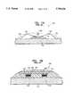
- FIG. 1Adescribes one structure of a radio frequency tag 105.
- the tag 105has a chip 110 mounted on a substrate 115.
- the chip 110has contacts 120 that are connected to circuitry on the substrate 115 by wire bonds 125.
- An encapsulation material 130covers the chip for environmental protection.
- the thickness of this tag 105is determined by the combined thicknesses of the chip components.
- substrates in these tagsare at least 10 mils, 0.25 mm, in thickness
- the chip 110 along with the high loop 122 of the bondvary from 20 to 40 mils, 0.5 to 1 mm, in thickness and the encapsulation 130 is about 10 mils, 0.25 mm in thickness.
- tags 105 of this structurevary from a minimum of 40 to 60 mils, 1 to 1.5 mm, in thickness. This structure is too thick for many potential tag applications.
- FIG. 1Bshows another structure 150 showing a chip 140 with the chip contacts 152 connected to circuitry contacts 155 with conducting adhesive 160.
- the substrate 165 of this structure 150is typically made as a FR4/printed circuit (thickness 40 to 60 mils, 1 to 1.5 mm) or flexible substrate (10 mils, 0.25 mm).
- the chip 140 and adhesive 160add another 20 to 40 mils, 0.5 to 1 mm, to the thickness and the encapsulation 165 adds still another 10 to 20, 0.25 to 0.5 mm mils in structure 150 thickness.
- This structuretherefore can vary in thickness from 80 to 130 mils, 2 to 3.5 mm, making it thicker than the structure in FIG. 1.
- Quad flat pakQFP
- SOPsmall outline pak
- leadframe structuresare known in the art.
- semiconductor memory chip packagingis disclosed in U.S. Pat. No. 4,916,519 to Ward, filed on May 30, 1989 and issued on Apr. 10, 1990.
- the structureincludes the use of an etched or stamped metal foil that is joined to the chip to be packaged.
- the chipis connected electrically to the leadframe by means of thin wirebond interconnections.
- the chip and the inner areas of the leadframeare encapsulated using a rigid organic molding compound. Elements of the leadframe protrude from the package so as to permit electrical connection by means of soldering to a circuit board.
- leadframe technologyfor the manufacture of RFID tags.
- the leadframeserves as a support structure for a chip and coil antenna and capacitor. Connections are made to the leadframe from the chip by means of thin wirebonding.
- the coil antennais electrically connected to the leadframe as may be a capacitor.
- the componentsare sealed using an organic plastic or epoxy molding compound. Elements of the metal leadframe extend outside of the molded portion of the package.
- the addition of the coil to the Eberhardt packageinsures that the package will be at least 1.5 mm, but most likely 2 to 3 mm thick.
- the Eberhardt package embodiment that shows a capacitorwill be at least 2 mm thick in order to include the bulk of the capacitor.
- the Eberhardt packageis too thick for inclusion in a credit card.
- One prior art referencediscloses a package with a total thickness of 0.8 mm. This is still greater than the ISO standard credit card thickness of 0.76 mm. Furthermore, while thin elements are disclosed, no care is taken to use flexible materials throughout. The components are mounted on a hard circuit card and encapsulated in plastic. (Hard means can not be torn easily by hand.) The result a is rigid package. Much of the prior art has not shown the use of thin flexible laminate covering materials for the packages. The results are that the packages are thick, and inflexible.
- the prior arthas also failed to make thin, flexible radio frequency transponders because there is at least one component, the antenna, that must be packaged external to the radio frequency circuit that is using the antenna to transmit/receive signals. Since there are at least these two components in prior art transponders, these components had to be mounted on some sort of substrate or circuit card in order to provide support for the components and to position the components relative to each other. These substrates/cards add thickness to and limit the flexibility of the package.
- the prior artoften needs structures in the transponder package used to connect, support, and position the antenna and chip components. These structures add complexity, thickness, and inflexibility to the package. Layers, in addition to the substrate/circuit board, are sometimes added to position the radio frequency circuit and antenna in three dimensions so that electrical bonds among the components can be made. For example, one substrate might be required to support and position the radio frequency circuit while one or more other layer of substrate might be required to support and raise the antenna to the elevation of connections on the radio frequency circuit.
- the antenna and connecting conductorsoften require more than one plane of electrical wiring, i.e., the designs use cross-overs for completing interconnections. Components are often are stacked one upon the next.
- the prior arthas not solved the problem of building a transponder package with a minimum of component support; a minimum of strong, thin, and flexible components; and a minimum of interconnections among components.
- Some prior arthas metal leadframe elements protruding from its packaging. These elements are not used for externally connections but result from the limitations of package structure design and the process used to manufacture it. These protruding elements cause several problems. Since they are connected internally to the chip, the chip may be damaged by electrostatic discharge damage (ESD). The protruding metal elements are lightning rods for ESD. In addition, in corrosive environments, tag packages with protruding metal are inadequate. For example, a requirement for laundry service is that the package provide resistance to corrosion. Chlorine bleaches containing large numbers of corrosion-inducing chlorine ions are used in the laundry process. The interface between the metal elements and the epoxy molding is a channel for the transport of chlorine ions into the package. The metal elements themselves may also corrode and dissolve as a result of their immersion in a chlorine ion rich laundry environment.
- An object of this inventionis an improved RF transponder apparatus.
- An object of this inventionis an improved thin, flexible RF tag apparatus that has a minimum of components and connections.
- An object of this inventionis an improved thin, flexible RF tag apparatus that has a minimum of components and connections that is completely protected by a protective surrounding.
- An object of this inventionis an improved thin, flexible RF tag apparatus that has a minimum of components and connections that are unsupported by a substrate layer.
- An object of this inventionis an improved thin, flexible RF tag that has components that are not rigidly attached to a protective surrounding so that shear forces between the protective surrounding and the components are reduced when the transponder is mechanically flexed.
- the present inventionis a novel radio frequency transponder (tag) that has a minimum of components and connects and that is thin and flexible because these components and connects can be unsupported by a substrate layer. This is accomplished by using a conducting leadframe structure not only as a connection medium but also as a circuit element, i.e., the transponder antenna.
- the leadframeis mechanically positioned and fixably attached to a circuit chip so that the leadframe (antenna) is self supporting.
- a protective coatingcan be added where the leadframe is attached to the circuit chip to protect the surface of the chip from corrosion and abrasion, to exclude light (in some embodiments) from impinging on the circuit chip, and to strengthen the mechanical connections of the leadframe antenna structure that are fixably attached to the electrical connectors on the circuit chip.
- some preferred embodimentshave a protective surrounding that envelops the entire leadframe antenna, circuit chip, and, if provided, the protective coating.
- the protective surroundingprovides resistance to corrosion and abrasion to the leadframe antenna and the circuit chip.
- the protective surroundingcan comprise more than one layer.
- the protective surroundingfurther can be made of materials that do not rigidly attach to the leadframe antenna so that shear forces between the leadframe antenna and the protective surrounding are reduced when the antenna is mechanically flexed.
- FIG. 1,comprising FIG. 1A and FIG. 1B, is a diagram showing the cross section of two typical known structures.
- FIG. 2is a drawing of a preferred embodiment of the present radio frequency circuit with a leadframe antenna in top view (FIG. 2A), elevation (FIG. 2B), elevation with protective coating (FIG. 2C), elevation with protective coating and surrounding (FIG. 2D), an elevation with protective surrounding (FIG. 2E), and an elevation with a protective coating sandwiched between the circuit and an overlayer where the protective coating forms a fillet region at the circuit edges (FIG. 2F).
- FIG. 3is a diagram showing the plan view (3A) and various cross sections (FIGS. 3B-3D) of a preferred RFID tag with a leadframe antenna and a protective surrounding.
- FIG. 4is a set of plan views showing example preferred alternative antenna designs that can be used with the present invention.
- FIG. 5is a diagram showing the plan view (FIG. 5A) and a cross sections (FIG. 5B) of a preferred structure having positioners attached to the off chip length of the lead frame antenna.
- FIG. 6is a plan view of the radio frequency circuit with a leadframe antenna and an alternative preferred positioner with a window.
- FIG. 7is a plan view of the radio frequency circuit with a leadframe antenna and alternative preferred positioners.
- FIG. 8comprising FIGS. 8A-8C, showing a plan view of "centering" circuit chip connectors (FIG. 8A), a plan view of alternative attachments to "centered" circuit chip connectors (FIG. 8B) and a side view (FIG. 8C) with a protective coating.
- FIG. 9is a side view of an alternative preferred embodiment showing the circuit chip supported by and wire bonded to the lead frame antenna structure.
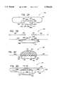
- FIG. 2Ais a plan view and FIG. 2B is a front view (elevation) of one preferred embodiment of the present invention.
- the embodimentcomprises a circuit chip that is a radio frequency transponder 210.
- the circuit chiphas a surface 215 and edges 265 (e.g. 265L, 265R, 265B, and 265T) with one or more connectors 220 (e.g. 220A and 220B) that connect to the circuitry within the circuit chip.
- the circuit chip 210also has a center portion 260 that is on the surface of the circuit chip, includes the connectors 220, and is a given distance 235 (e.g. 235L, 235R, 235B, and 235T) from any of the respective circuit chip edges 265.
- this circuitrytypically includes a radio frequency circuit for receiving and transmitting radio frequency signals, a memory for storing information, and logic and other digital circuits for control and communication protocols.
- Circuit 210like this are well known. See for example the Anders patent incorporated above. Another novel, circuit is disclosed in U.S. patent application Ser. No. 08/303,965 to Cesar et al. filed on Sep. 9, 1994 that is herein incorporated by by reference in its entirety. While the most preferred use of this invention is that of a circuit chip 210 that is a radio frequency transponder, specifically an RFID tag, any semiconductor chip circuit 210 can be can be attached to a lead frame structure in the manner embodying this invention.
- the antenna 200is constructed from a leadframe.
- This leadframe antenna 200is made from a material that is electrically conductive and has a degree of stiffness that permits the antenna to flex within a given amount when supported at one or more ends.
- the stiffnessis characterized by Young's Modulous which is defined as the stress require to produce a unit of strain.
- the strainmay be a change of length.
- the desired range of Young's Modulus of the leadframe materialis on the order of 12 ⁇ 10exp11 dynes per square cm (17.5 ⁇ 10exp6 pounds per square inch) or greater.
- the leadframe antenna 200can be designed in various shapes that are described below.
- the leadframe antenna 200will have at least two ends (200A, 200B) at least one 200A of which is electrically attached 225 to one of the connectors 220 of the circuit chip 210.
- the end of the leadframe 200 that is fixably attached 225has any of the following end shapes: flat, crescent, off set, angle, and ball.
- the leadframe antenna 200will also have a section called an overlapping length 230 that overlaps the surface 215 of the circuit chip 210.
- the overlapping length 230is the portion or portions of the leadframe antenna 200 that is between an electrical connection 225 of one end 200A of the antenna 200 and a connector 200 and an edge 265 of the circuit chip 210.
- the overlapping length 230includes the point of electrical (an mechanical) attachment 225.
- An off chip length 240 of the antenna 200is that portion of the antenna that does not overlap the surface 215 but that is suspended past any of the edges 265.
- the leadframe antenna 200is also mechanically attached to the circuit chip so that it is fixed to the chip at one or more locations on the overlapping length. One of these locations will be the point of electrical connection 225 between the leadframe antenna 200 end 200A, 200B and the connector 220A, 220B, respectively. This fixable attachment permits no mechanical movement at the point of attachment 225A,B. Any prior art connection that provides a fixed mechanical and an electrical connection between the leadframe antenna 200 end (200A, 200B) can be used.
- the fixed attachmentcan include other mechanical attachments between the overlapping length(s) 230 and the circuit chip 210 and/or chip surface 215.
- the fixed attachmentincludes the adhesive effects of a protective coating (described below) that is placed between the overlapping length 230 and the chip surface 215 and/or in other locations to attach the overlapping length 230 to the surface 215 so that there is no movement between the overlapping length 230 and the surface 215.
- a leadframeis a punched and/or etched foil. (See FIG. 6 description below.)
- the materials usedare generally copper, copper-alloys, or nickel-iron alloys such as alloy-42. Other electrically conductive materials are envisioned.
- FIG. 2Cis a elevation showing the circuit chip 210 with the leadframe antenna 200 that has a protective coating 270.
- the protective coatingcovers the circuit chip surface 215 and overlaps the ends (200A, 200B) of the leadframe 200.
- the protective coating 270also overlaps one or more edges 265 of the circuit chip 210 so that the ends (200A,B) of the antenna are mechanically fixed to the chip surface 215 and the chip sides 266.
- Flowing the protective coating around the chip sides 266,assures that the chip surface 215 is fully covered. This also assures better adhesion of the protective coating 270 to the entire circuit chip surface 215.
- the flowing of the protective coating over 266 the chip surface 215 and sides 265further give more support and mechanical strength to the ends (200A,B) of the leadframe.
- the protective coating 270is made of a polymer material such as epoxies, silicones and urethanes, also known as isocyanates or polyurethanes, which are thermosetting. Additional protective coatings include photopolymers or ultraviolet (uv) curing materials.
- FIG. 2Dshows the invention shown in FIG. 2C in an elevation view with protective coating 270 and a protective surrounding 280.
- the protective surroundingcomprises two layers, an inner layer 285 and an outer layer 283.
- the entire protective surrounding 280is made with one layer.
- the protective surrounding 280provides environmental protection for the circuit chip 215 and leadframe 200.
- the protective surrounding 280prevents moisture, chemicals, contaminants, corrosive materials, etc. from attacking the circuit chip 215, connections 220, and leadframe 200.
- the protective surround 280also provides mechanical protection from the lead frame against impact, abrasion, cutting, etc. Further the protective surround provides a packaging media providing printing information and a handling media for the transponder.
- the protective surround 280can be cardboard or paper, (e.g. a postal package/letter, credit card, or passport, that is used to house to the transponder 250.
- the protective surrounding 280can be made of any one of the following materials: paper, cardboard thermosetting, thermoplastic, or pressure sensitive materials: ethylene acetate, polystyrene, polycarbonate, polypropylene, polyethylene, polyurethane, polyester, polyolefin, nylon, vinyl, silicones, rubber based adhesives, acrylic adhesive, and water soluble adhesives and polyethylene terephthalete (PET), polyethylene naphthalate (PEN), polyetherimide (PEI), polyetheretherketone (PEEK), polysulfone (PS), polyphenylene sulfone (PPS), and polyethersulphone (PES), polyvinyl chloride (PVC), polyester (Mylar), and polyimide (Kapton).
- PETpolyethylene naphthalate
- PENpolyetherimide
- PEEKpolyetheretherketone
- PSpolysulfone
- PPSpolyphenylene sulfone
- PESpolyethersulphone
- PVCpolyvinyl
- the protective surrounding 280can be applied in two layers (283, 285).
- the inner layer 285would have good adhesive and flow characteristics that would cause it to bond well to the leadframe 200 and chip 210 so that the transponder 250 will not delaminate.
- the outer layer 283preferably will be resilient and tough to protect the transponder 250 from the environment and mechanical stresses.
- Preferred materials used for the inner layer 285include: ethylene vinyl acetate, acrylic, silicone, rubber, modified epoxies, phenolic, polyester, polyimide, as well as fluoropolymer based adhesives.
- Materials used for the outter layer (and/or a single layer of protective surrounding 280)include: paper, cardboard, polyethylene terephthalete (PET), polyethylene naphthalate (PEN), polyetherimide (PEI), polyetherether ketone (PEEK), polysulfone (PS), polyphenylene sulfone (PPS), and polyethersulphone (PES), polyvinyl chloride (PVC), polyester (Mylar), and polyimide (Kapton).
- the protective surrounding 280(or 283/285) completed surrounds the circuit chip 210 and leadframe 200. This is to protect the leadframe 200 and chip 210 from attack of environmental agents, including electrical sparks, through any path through the protective surrounding 280.
- FIG. 2Eis an elevation view of a transponder 250 that has a single layer of protective surrounding 280 and no protective coating 270.
- This embodimenttypically would be injection molded by known techniques.
- This embodimentcan be made as a rigid package and any shape and offers very good mechanical support and environmental protection for the leadframe 200 and circuit chip 215.
- Transponders 250can be enveloped in injection molded plastic housing that are used as toys, machine parts, covers and containers, etc.
- FIG. 2Fis an elevation view showing a preferred embodiment of the transponder 250.
- the transponder 250has a protective coating 270 sandwiched between the circuit chip 210 and an overlayer 290.
- the protective coating 270forms a fillet region 295 between the circuit edges (sides 265) and the underside of the leadframe 200.
- the overlayer 290acts as a guide for the protective coating 270 which flows into the region 292 between the overlayer and the chip surface 215 as the protective coating 270 "wicks" from the under side of the leadframe 200.
- the overlayer 290accurately determines the thickness of the protective coating 270 by defining the region 292 and also insures that protective coating 270 completely covers the chip surface 215.
- the fillets 295offer additional mechanical support of the leadframe 200 and bounding of the leadframe 200 to the chip 210.
- the overlayerhas a length, width, and position over the chip surface 215 that causes the overlayer to extend past the connectors 220 on the chip 210. In another preferred embodiment, the overlayer has a length and position that causes the overlayer to extend past the sides 265 of the chip 210 This is done so as to form a better fillet 295.
- FIGS. 2A-2Fshow that in one preferred embodiment of the transponder, there is only one plane of conductive material (e.g., metalization) which is the leadframe antenna 200.
- the connectors 220 on the chip surface 215fall slightly out of this plane by a very small amount, i.e., the thickness of the connector 220 and the connection 215.
- Thisis made possible by the stiffness of the leadframe antenna 200 and the fixed mechanical attachment of the antenna at the connector (and other places if the protective coating 270 and surround 280 are used.) Since there is only one layer of conductive material, the transponder is more flexible has a thin profile.
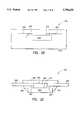
- FIG. 3is a diagram showing the plan view (FIG. 3A) and various cross sections (FIGS. 3B-3D) of a preferred RFID tag with a leadframe antenna and a protective surrounding 280.
- FIG. 3Ashows an elevation of the transponder 250 with cross sections taken at the: off chip 240 parts of the leadframe antenna 200 (AA); overlapping length 230 of the frame antenna 200, specifically at the connection 225 (BB); and part(s) of the transponder where there is no leadframe antenna 200 (CC).
- FIG. 3Bshows a cross section(s) (AA) of the transponder 250 at the off chip length 240 of the leadframe antenna 200.
- the only componentsare the leadframe antenna (200, 320) surrounded by the protective surrounding 280.
- the leadframe antenna 200is suspending in and surrounded by the protective surrounding 280 with no other supporting structure, e.g. a substrate. Therefore, this transponder 250 can be very thin because the only structures required in the off chip 240 sections of the transponder 250 (and leadframe antenna 200 of the transponder 250) are the leadframe antenna 200 element and the protective surrounding 280.
- the transponder 250is thin, it is mechanically strong and environmentally resistant because of the combined strength of the leadframe 200 and the protective surrounding 280.
- FIG. 3Cshows a cross section (BB) of the transponder 250 a the chip 210 with the ends 210 overlapping a portion or length 230 of the chip surface 215. (This cross section is specifically at the connection 225.) This cross section also shows the protective coating 270 and the leadframe 200 end 200A connected to the chip connector 220.
- FIG. 3Dshows a cross section (CC) of the transponder 250 taken at a point where there is no leadframe 200.
- This cross sectioncomprises only protective surrounding 280 and illustrates that the transponder 250 is completely surrounded by the protective surrounding 280 so that no path exists for environmental contaminants to enter and attack the leadframe 200, leadframe end 200A,B, connections 220, and/or chip 210.
- protective surround 280 described in FIG. 3could also comprise and inner 285 and an outer 283 layer as disclosed above.
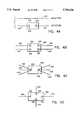
- FIG. 4shows various leadframe antenna structures that are created by stamping and/or etching various shapes on the leadframe metal. Again, the off chip length can be suspended with with no substrate or other support due to the stiffness of the leadframe 200 (420). See definition of Young's Modulus above.
- FIG. 4Athere is a dipole antenna 420 attached to the chip 210 connector 220 along with a parasitic element 421 like a antenna director or reflector.
- a double dipole antenna 420is stamped and/or etched and attached (electrically and mechanically) to a connector 210 on the chip 400.
- chips 400are variations of chip 210.
- chip 400has two pairs of connectors 220.
- the two dipoles 420can be of different lengths and therefore of different frequencies controlled by two separate oscillators on the chip 400.
- the leadframe antenna structureis a "whisker structure" that has multiple elements to improve the range and directionality of the antenna.
- two dipolar antennas 420are stamped and/or etched from the leadframe to produce an antenna that has elements that are orthogonal or nearly orthogonal so that the range and directionality of the antenna is enhanced.
- FIG. 4Eshows a monopolar antenna 460.
- FIG. 4Fshows a single loop antenna 450
- FIG. 4Gshows a multiple loop antennas 455 (A,B).
- FIG. 4His a top view as shown in FIG. 4A with the addition of two dummy chip contacts 480.
- the dummy contacts 480are connected by a dummy metal connector 411 with a protruding piece 412.
- the dummy contacts 480 with the dummy metal connector 411provide a mechanical structure on the opposite side of the chip from the antenna connections 220.
- the protrusion 412provides a connection to an unused portion of the leadframe for mechanical support while the chip 400 is being attached to the leadframe antenna 420 (with optional 421.) After the chip 400 is attached to the leadframe antenna, the protrusion 412 is cut. See “Method of Making a Thin Radio Frequency Transponder", to Brady et al., U.S. patent application Ser. No. 08/621,385, filed on the same day as this application to Brady et al., which is herein incorporated by reference in its entirety.
- the leadframe antenna antenna 420 and/or the dummy mechanical connector 411can be connected to the chip contacts 220 (dummy contacts 480) by any one or more known connection methods including compression bonding, ultrasonic bonding, thermal sonic bonding, and laser sonic bonding.
- compression bondingultrasonic bonding
- thermal sonic bondingthermal sonic bonding
- laser sonic bondingfor some bonding techniques see U.S. patent application Ser. No. 08/330,288 entitled Method of Making Radio Frequency Identification Tags, to Brady et al. filed on Oct. 27, 1994.
- All these various antenna structures described above, and others,can be electrically connected to the chip (210, 400), with protective coatings 270, and/or protective surrounds 280 as described in FIG. 2 above.
- FIG. 5Ais a plan view of one preferred embodiment of the present leadframe structure 530 using positioners 540 to position the leadframe elements of the leadframe antenna 520 (200, 420, etc.).
- a positioner 540is an organic film strip or tape that maintains the position of the leadframe antenna 520 with respect to the chip 210, 400, etc.) and also provides additional support for the antenna 520.
- the positioners 540provide extra strength for the antenna elements 520 during the assembly process when the antenna elements 520 are attached to the chip contacts 220 and further are cut from any unused portion of the leadframe that may be providing support before the leadframe antenna 520 is packaged in structure 530.
- antenna 520can be any of the antenna embodiments described above and the chip can be any of the chips described above.
- the positioners 540are typically between 10 and 125 microns in thickness. More preferably, they 540 are between 15 and 50 microns in thickness. Examples of materials used for the positioners 540 include: thermosetting materials; thermoplastic materials; or polyimide. Mylar (polyester) is a material which may be used.
- the positioners 540are placed as close as possible to the chip 210. In a preferred embodiment, this distance 545 is between 0.15 and 0.75 millimeters. More preferably, the distance about is 0.175 to 0.5 millimeters. However, this distance is dictated by current manufacturing technology. If this manufacturing technology would allow closer placement of the positioners 540 to the chip without infringing on the surface of the chip, closer placement of the positioners 540 would be used, if cost effective.
- the positioners 540have a positioner width 560 between 0.25 and 5 millimeters. More preferably, the positioner width 560 is between 0.5 and 2.5 millimeters.
- the distance 545needs to insure proper wicking (see, for example, FIGS. 2C and 2F) of any encapsulant that would cover the chip along with the leadframe antenna end (200A, B) connected to the contact 225 and overrun onto the sides 265 of the chip to form a "fillet. (266, 295)"
- the gap distance 545should be wide enough so that the encapsulant 270 can flow but not too wide so that the encapsulant fall through the gap 545. In practice the gap distance 545 should be at least 0.18 millimeters (about 7 mils.)
- FIG. 5Bis a cross section A--A of Figure SA showing the leadframe antenna element 520 and the positioner 540 enclosed in the protective surrounding 280.
- the positionersare located on the same side of the leadframe as is the chip. This is done so as to not increase the thickness of the total package. If both the chip and the positioners are attached on the same side of the leadframe, the maximum thickness of this part of the package is that of the leadframe plus that of the thickest of the chip or the positioners. If the chip and the positioners were on opposite sides of the leadframe, the total thickness would be the sum of the thickness of all three elements.
- FIG. 6is a plan view of the radio frequency circuit with a leadframe antenna (620, 621) (or any of others described above) and an alternative preferred positioner 640.
- This positioner 640has a positioner width 610 that is wide enough to cover the chip (210, 400, etc.) and two times the gap (typically 615 or the sum of the gaps 615L and 615R), while still overlapping 625 some of the leadframe antenna 620.
- the gaps 615 on the (right 615R and left 615L) sides of the chip 210 and the gaps 620 on the top 630T and bottom 630B sides of the chipform a window 650 in which the chip 210 sits.
- all the gaps (615L, 615R, 630T, 630B)are wide enough to allow an encapsulant to flow between the chip 210 sides 265 and the positioner 640 so that the encapsulant wicks and forms a fillet attaching to the sides 265 of the chip 210.
- This embodimentrequires that the manufacturing process position the chip 210 within the window 650 so that the correct gaps (615, 630) are created.
- the positioner 640can be made as thick and made of the same material as the positioners described above.
- FIG. 7is a plan view of the radio frequency circuit with a leadframe antenna 420 (421) and alternative preferred positioners 740 that are positioned on either side of the chip (210, 400, etc.).
- the gaps 715 on the left 715L and right 715R sides of the chip 210form a trough or channel 730 in which the chip 210 sits.
- the gaps 715are wide enough to allow an encapsulant to flow between the sides 265 of the chip 210 and the positioner(s) 740 so that the encapsulant wicks and forms a fillet attaching to the side(s) 265 of the chip 210.
- the positioners 740can be made as thick and made of the same material as the positioners described above. Typically the positioners 740 have a positioner width 760 between 0.25 and 5 millimeters. More preferably, the positioner width 760 is between 0.5 and 2.5 millimeters. The positioners 740 are placed preferably so that the gap 715 is 0.5 mm or less, and more preferable so that the gap 715 is 0.25 mm or less.
- FIG. 8shows a plan view of "centering" circuit chip connectors 220 (FIG. 8A), a plan view of alternative attachments to "centered" circuit chip connectors 220 (FIG. 8B) and a side view (FIG. 8C) with a protective coating 270.
- Positioning the connectors in this mannerreduces or removes the requirement for positioners (540, 640, and 740) to hold the encapsulant 270 so as to form a dome of encapsulant 270 over the chip.
- the lea(1frame antenna leads 200are positioned over 230 and bonded 225 to the chip connectors 220 on chip 210.
- the chip connectors 220are located a minimum distance 815 from each of the sides 265 of the chip 210. Specifically, the connectors are located on the chip surface 215 at: a distance 815L from the left side 265L, a distance 815R from the right side 265R, a distance 815B from the bottom side 265B, a distance 815T from the left side 265T of the chip 210. Placement of the chip connectors 220 in this manner "centers" the chip connectors in a center region 850 on the surface of the chip 210.
- the distance 815is between 0.25 mm and 0.5 mm. More preferably the distance 815 is about one quarter of the width of chip for small chips.
- one or more of the leadframe antenna elements 801has a bend 860. This is done so as to releave the stress from mechanical bending or thermal mismatch of expansion coefficients of the different materials of the package.
- a dome of encapsulated 270is deposited over (the chip 210 in such a way as to cover the chip connectors 225 with a protective coating 270.
- FIG. 9is a side view of an alternative preferred embodiment 900 of the present structure showing the circuit 210 supported by and bonded to the leadframe antenna 920 (200 etc.) structure.
- the wirebond wires 901are bonded to the leadframe antenna 920 to form connections 935 to the antenna 920.
- the wires 901are bonded 225 to the connection pads 220 on the chip 210 at their chip termination ends (200A,B).
- the chip 210is located on the leadframe 920 while the whole structure is surrounded by a protective material 280.
- any one of the antenna structures disclosedcould be used with any one of the positioniers disclosed.
- no positionerscould be used.
- the radio frequency packagemay or may not use any one of the protective coating and/or protective surrounds.
Landscapes
- Engineering & Computer Science (AREA)
- Microelectronics & Electronic Packaging (AREA)
- Physics & Mathematics (AREA)
- General Physics & Mathematics (AREA)
- Computer Hardware Design (AREA)
- Power Engineering (AREA)
- Condensed Matter Physics & Semiconductors (AREA)
- Theoretical Computer Science (AREA)
- Details Of Aerials (AREA)
- Radar Systems Or Details Thereof (AREA)
- Lead Frames For Integrated Circuits (AREA)
- Support Of Aerials (AREA)
- Near-Field Transmission Systems (AREA)
Abstract
Description
Claims (32)
Priority Applications (5)
| Application Number | Priority Date | Filing Date | Title |
|---|---|---|---|
| US08/621,784US5786626A (en) | 1996-03-25 | 1996-03-25 | Thin radio frequency transponder with leadframe antenna structure |
| TW085114138ATW343323B (en) | 1996-03-25 | 1996-11-18 | Thin radio frequency transponder with leadframe antenna structure |
| KR1019960066064AKR100216147B1 (en) | 1996-03-25 | 1996-12-14 | Radio frequency transponder |
| SG1997000626ASG54473A1 (en) | 1996-03-25 | 1997-03-01 | Thin radio frequency transponder with leadframe antenna structure |
| JP05482397AJP3980697B2 (en) | 1996-03-25 | 1997-03-10 | Wireless transponder |
Applications Claiming Priority (1)
| Application Number | Priority Date | Filing Date | Title |
|---|---|---|---|
| US08/621,784US5786626A (en) | 1996-03-25 | 1996-03-25 | Thin radio frequency transponder with leadframe antenna structure |
Publications (1)
| Publication Number | Publication Date |
|---|---|
| US5786626Atrue US5786626A (en) | 1998-07-28 |
Family
ID=24491625
Family Applications (1)
| Application Number | Title | Priority Date | Filing Date |
|---|---|---|---|
| US08/621,784Expired - LifetimeUS5786626A (en) | 1996-03-25 | 1996-03-25 | Thin radio frequency transponder with leadframe antenna structure |
Country Status (5)
| Country | Link |
|---|---|
| US (1) | US5786626A (en) |
| JP (1) | JP3980697B2 (en) |
| KR (1) | KR100216147B1 (en) |
| SG (1) | SG54473A1 (en) |
| TW (1) | TW343323B (en) |
Cited By (210)
| Publication number | Priority date | Publication date | Assignee | Title |
|---|---|---|---|---|
| US5939984A (en)* | 1997-12-31 | 1999-08-17 | Intermec Ip Corp. | Combination radio frequency transponder (RF Tag) and magnetic electronic article surveillance (EAS) material |
| US5946198A (en)* | 1994-10-21 | 1999-08-31 | Giesecke & Devrient Gmbh | Contactless electronic module with self-supporting metal coil |
| US5955949A (en)* | 1997-08-18 | 1999-09-21 | X-Cyte, Inc. | Layered structure for a transponder tag |
| US5972156A (en)* | 1994-09-09 | 1999-10-26 | Intermec Ip Corp. | Method of making a radio frequency identification tag |
| US5992739A (en)* | 1996-08-09 | 1999-11-30 | Ferag Ag | Movable object carrying electronically stored data to be read and or/overwritten by a non-contact reading/writing device |
| US6018299A (en)* | 1998-06-09 | 2000-01-25 | Motorola, Inc. | Radio frequency identification tag having a printed antenna and method |
| US6040773A (en)* | 1995-10-11 | 2000-03-21 | Motorola, Inc. | Radio frequency identification tag arranged for magnetically storing tag state information |
| WO2000016285A1 (en)* | 1998-09-11 | 2000-03-23 | Motorola Inc. | An integrated circuit assembly and method of assembly |
| WO2000016286A1 (en)* | 1998-09-11 | 2000-03-23 | Motorola Inc. | Radio frequency identification tag apparatus and related method |
| US6043745A (en)* | 1997-11-13 | 2000-03-28 | Micron Technology, Inc. | Electronic devices and methods of forming electronic devices |
| WO2000021030A1 (en)* | 1998-10-06 | 2000-04-13 | Intermec Ip Corp. | Rfid transponder having improved rf characteristics |
| WO2000023994A1 (en)* | 1998-10-16 | 2000-04-27 | Intermec Ip Corp. | Smart optical storage media |
| WO2000036555A1 (en) | 1998-12-17 | 2000-06-22 | Hitachi, Ltd. | Semiconductor device and production method thereof |
| US6100804A (en)* | 1998-10-29 | 2000-08-08 | Intecmec Ip Corp. | Radio frequency identification system |
| US6104291A (en)* | 1998-01-09 | 2000-08-15 | Intermec Ip Corp. | Method and apparatus for testing RFID tags |
| US6107920A (en)* | 1998-06-09 | 2000-08-22 | Motorola, Inc. | Radio frequency identification tag having an article integrated antenna |
| US6114962A (en)* | 1998-10-15 | 2000-09-05 | Intermec Ip Corp. | RF tag having strain relieved stiff substrate and hydrostatic protection for a chip mounted thereto |
| US6121878A (en)* | 1998-05-01 | 2000-09-19 | Intermec Ip Corp. | System for controlling assets |
| US6130613A (en)* | 1998-06-09 | 2000-10-10 | Motorola, Inc. | Radio frequency indentification stamp and radio frequency indentification mailing label |
| US6177872B1 (en) | 1998-03-13 | 2001-01-23 | Intermec Ip Corp. | Distributed impedance matching circuit for high reflection coefficient load |
| US6177859B1 (en)* | 1997-10-21 | 2001-01-23 | Micron Technology, Inc. | Radio frequency communication apparatus and methods of forming a radio frequency communication apparatus |
| WO2001009829A1 (en)* | 1999-08-03 | 2001-02-08 | Intermec Ip Corp. | Automated rfid transponder manufacturing on flexible tape substrates |
| WO2000059067A3 (en)* | 1999-03-29 | 2001-02-22 | Intermec Ip Corp | Antenna structure for wireless communications device, such as rfid tag |
| US6201474B1 (en) | 1998-10-21 | 2001-03-13 | Intermec Ip Corp. | Magnetic tape storage media having RFID transponders |
| US6211565B1 (en)* | 1999-04-29 | 2001-04-03 | Winbond Electronics Corporation | Apparatus for preventing electrostatic discharge in an integrated circuit |
| US6215402B1 (en)* | 1998-03-13 | 2001-04-10 | Intermec Ip Corp. | Radio frequency identification transponder employing patch antenna |
| US6229442B1 (en) | 2000-03-14 | 2001-05-08 | Motorola, Inc, | Radio frequency identification device having displacement current control and method thereof |
| US6236223B1 (en) | 1998-11-09 | 2001-05-22 | Intermec Ip Corp. | Method and apparatus for wireless radio frequency testing of RFID integrated circuits |
| US6236316B1 (en) | 1999-01-05 | 2001-05-22 | Motorola, Inc. | Transport device with openings for capacitive coupled readers |
| US6246327B1 (en) | 1998-06-09 | 2001-06-12 | Motorola, Inc. | Radio frequency identification tag circuit chip having printed interconnection pads |
| FR2802684A1 (en)* | 1999-12-15 | 2001-06-22 | Gemplus Card Int | DISPOSABLE INTEGRATED CIRCUIT CHIP DEVICE AND METHOD FOR MANUFACTURING SUCH A METHOD |
| US6252508B1 (en) | 1995-10-11 | 2001-06-26 | Motorola, Inc. | Radio frequency identification tag arranged for magnetically storing tag state information |
| US6271793B1 (en)* | 1999-11-05 | 2001-08-07 | International Business Machines Corporation | Radio frequency (RF) transponder (Tag) with composite antenna |
| US6275681B1 (en) | 1998-04-16 | 2001-08-14 | Motorola, Inc. | Wireless electrostatic charging and communicating system |
| US6281794B1 (en) | 1998-01-02 | 2001-08-28 | Intermec Ip Corp. | Radio frequency transponder with improved read distance |
| US6282407B1 (en) | 1998-04-16 | 2001-08-28 | Motorola, Inc. | Active electrostatic transceiver and communicating system |
| US6285324B1 (en)* | 1999-09-15 | 2001-09-04 | Lucent Technologies Inc. | Antenna package for a wireless communications device |
| EP1054346A3 (en)* | 1999-05-21 | 2001-09-12 | Shinko Electric Industries Co. Ltd. | Non-contact chip card comprising a pair of covering sheets |
| US6320556B1 (en) | 2000-01-19 | 2001-11-20 | Moore North America, Inc. | RFID foil or film antennas |
| US6329915B1 (en)* | 1997-12-31 | 2001-12-11 | Intermec Ip Corp | RF Tag having high dielectric constant material |
| US6362738B1 (en) | 1998-04-16 | 2002-03-26 | Motorola, Inc. | Reader for use in a radio frequency identification system and method thereof |
| US6366260B1 (en) | 1998-11-02 | 2002-04-02 | Intermec Ip Corp. | RFID tag employing hollowed monopole antenna |
| US6369711B1 (en)* | 2000-06-09 | 2002-04-09 | Intermec Ip Corp | Profile corrected label with RFID transponder and method for making same |
| US6377176B1 (en)* | 2000-06-13 | 2002-04-23 | Applied Wireless Identifications Group, Inc. | Metal compensated radio frequency identification reader |
| US20020047130A1 (en)* | 2000-06-28 | 2002-04-25 | Koay Huck Khim | Light Source |
| US6392544B1 (en) | 2000-09-25 | 2002-05-21 | Motorola, Inc. | Method and apparatus for selectively activating radio frequency identification tags that are in close proximity |
| US6404339B1 (en) | 1995-10-11 | 2002-06-11 | Motorola, Inc. | Radio frequency identification tag arranged with a printable display |
| US6411213B1 (en) | 1995-10-11 | 2002-06-25 | Motorola, Inc. | Radio frequency identification tag system using tags arranged for coupling to ground |
| US20020098623A1 (en)* | 2000-08-31 | 2002-07-25 | Salman Akram | Semiconductor device including leads in communication with contact pads thereof and a stereolithographically fabricated package substantially encapsulating the leads and methods for fabricating the same |
| US6441740B1 (en) | 1998-02-27 | 2002-08-27 | Intermec Ip Corp. | Radio frequency identification transponder having a reflector |
| US6457337B1 (en) | 2000-06-14 | 2002-10-01 | Motorola, Inc. | Key, lock, and key and lock system |
| FR2824018A1 (en)* | 2001-04-26 | 2002-10-31 | Arjo Wiggins Sa | COVER INCORPORATING A RADIO FREQUENCY IDENTIFICATION DEVICE |
| US20020167500A1 (en)* | 1998-09-11 | 2002-11-14 | Visible Techknowledgy, Llc | Smart electronic label employing electronic ink |
| EP1136943A3 (en)* | 2000-03-16 | 2002-11-27 | Andreas Dr. Plettner | Transponder |
| US6496112B1 (en) | 1998-02-27 | 2002-12-17 | Motorola, Inc. | Radio frequency identification tag with a programmable circuit state |
| US20020193047A1 (en)* | 2000-10-20 | 2002-12-19 | Weston Denise Chapman | Children's toy with wireless tag/transponder |
| US20030008323A1 (en)* | 1999-04-15 | 2003-01-09 | Ilya Ravkin | Chemical-library composition and method |
| US6509217B1 (en) | 1999-10-22 | 2003-01-21 | Damoder Reddy | Inexpensive, reliable, planar RFID tag structure and method for making same |
| US20030036096A1 (en)* | 1999-04-15 | 2003-02-20 | Ilya Ravkin | Chemical-library composition and method |
| US6531964B1 (en) | 1999-02-25 | 2003-03-11 | Motorola, Inc. | Passive remote control system |
| WO2003023705A1 (en)* | 2001-09-13 | 2003-03-20 | Alcoa Closure Systems International, Inc. | Method of making interactive information closure |
| US20030052396A1 (en)* | 2001-09-20 | 2003-03-20 | Kabushiki Kaisha Tokai Rika Denki Seisakusho | Semiconductor device and method of making the same |
| WO2003023706A1 (en)* | 2001-09-13 | 2003-03-20 | Alcoa Closure Systems International, Inc. | Method of making interactive information closure and package |
| US20030059764A1 (en)* | 2000-10-18 | 2003-03-27 | Ilya Ravkin | Multiplexed cell analysis system |
| WO2003038745A1 (en)* | 2001-10-31 | 2003-05-08 | Sokymat S.A | Transponder ic with optimized dimensions |
| US6563464B2 (en) | 2001-03-19 | 2003-05-13 | International Business Machines Corporation | Integrated on-chip half-wave dipole antenna structure |
| US20030107486A1 (en)* | 2001-09-28 | 2003-06-12 | Hitachi, Ltd. | Method for manufacturing electronic tag |
| US6580369B1 (en) | 1995-10-11 | 2003-06-17 | Motorola, Inc. | Electronic tag assembly and method therefor |
| US20030129654A1 (en)* | 1999-04-15 | 2003-07-10 | Ilya Ravkin | Coded particles for multiplexed analysis of biological samples |
| US20030134330A1 (en)* | 1999-04-15 | 2003-07-17 | Ilya Ravkin | Chemical-library composition and method |
| US6608561B2 (en)* | 1998-05-19 | 2003-08-19 | Meat Processing Service Corp., Inc. | Method for making a radio frequency identification device |
| US20030166015A1 (en)* | 1999-04-15 | 2003-09-04 | Zarowitz Michael A. | Multiplexed analysis of cell-substrate interactions |
| US6639509B1 (en) | 1998-03-16 | 2003-10-28 | Intermec Ip Corp. | System and method for communicating with an RFID transponder with reduced noise and interference |
| US20030207249A1 (en)* | 1999-04-15 | 2003-11-06 | Beske Oren E. | Connection of cells to substrates using association pairs |
| US6646554B1 (en) | 1998-06-08 | 2003-11-11 | 3M Innovative Properties Company | Identification tag with enhanced security |
| US20030219800A1 (en)* | 2001-10-18 | 2003-11-27 | Beske Oren E. | Multiplexed cell transfection using coded carriers |
| EP1284320A3 (en)* | 2001-08-16 | 2003-12-17 | Panther Packaging GmbH & Co.KG | Process for making corrugated board containing a transponder, and corrugated board containing a transponder |
| US20040026519A1 (en)* | 2002-08-08 | 2004-02-12 | Mitsuo Usami | Semiconductor devices and manufacturing method therefor and electronic commerce method and transponder reader |
| US20040033833A1 (en)* | 2002-03-25 | 2004-02-19 | Briggs Rick A. | Interactive redemption game |
| US6696952B2 (en) | 2000-08-04 | 2004-02-24 | Hei, Inc. | Structures and assembly methods for radio-frequency-identification modules |
| US20040041262A1 (en)* | 2002-08-28 | 2004-03-04 | Renesas Technology Corp. | Inlet for an electronic tag |
| US20040061613A1 (en)* | 2001-03-13 | 2004-04-01 | Hitachi, Ltd. | Electronic device and method of manufacture the same |
| US20040077423A1 (en)* | 2001-11-16 | 2004-04-22 | Weston Denise Chapman | Interactive quest game |
| US20040078957A1 (en)* | 2002-04-24 | 2004-04-29 | Forster Ian J. | Manufacturing method for a wireless communication device and manufacturing apparatus |
| US20040096911A1 (en)* | 1999-04-15 | 2004-05-20 | Oleg Siniaguine | Particles with light-polarizing codes |
| US6753830B2 (en) | 1998-09-11 | 2004-06-22 | Visible Tech-Knowledgy, Inc. | Smart electronic label employing electronic ink |
| US20040126773A1 (en)* | 2002-05-23 | 2004-07-01 | Beske Oren E. | Assays with coded sensor particles to sense assay conditions |
| US20040125040A1 (en)* | 2002-12-31 | 2004-07-01 | Ferguson Scott Wayne | RFID device and method of forming |
| US20040166827A1 (en)* | 1998-02-12 | 2004-08-26 | Micron Technology, Inc. | Thin profile battery bonding method of conductively interconnecting electronic components, battery powerable apparatus, radio frequency communication device, and electric circuit |
| US6782601B2 (en) | 2001-09-13 | 2004-08-31 | Alcoa Closure Systems International | Method of making interactive information closure |
| US20040198517A1 (en)* | 2002-08-01 | 2004-10-07 | Briggs Rick A. | Interactive water attraction and quest game |
| US20040204240A1 (en)* | 2000-02-22 | 2004-10-14 | Barney Jonathan A. | Magical wand and interactive play experience |
| US20040206799A1 (en)* | 2003-04-17 | 2004-10-21 | Wong Chi Ming | Method and apparatus for making smart card solder contacts |
| US20050051624A1 (en)* | 2003-09-08 | 2005-03-10 | Kipp Timo W. | Apparatus and method for detecting tampering with containers and preventing counterfeiting thereof |
| US6879809B1 (en) | 1998-04-16 | 2005-04-12 | Motorola, Inc. | Wireless electrostatic charging and communicating system |
| US20050084914A1 (en)* | 2003-09-15 | 2005-04-21 | Foulkes J. G. | Assays with primary cells |
| US20050084423A1 (en)* | 2003-09-15 | 2005-04-21 | Zarowitz Michael A. | Systems for particle manipulation |
| US20050093701A1 (en)* | 2003-11-04 | 2005-05-05 | Chep International, Inc. | RFID tag-pallet |
| US20050127155A1 (en)* | 2003-12-12 | 2005-06-16 | Claessens Francis M. | Apparatus for electronically determining whether a tax for a product has been paid |
| US20050143173A1 (en)* | 2000-02-22 | 2005-06-30 | Barney Jonathan A. | Magical wand and interactive play experience |
| US6921860B2 (en) | 2003-03-18 | 2005-07-26 | Micron Technology, Inc. | Microelectronic component assemblies having exposed contacts |
| US6924781B1 (en) | 1998-09-11 | 2005-08-02 | Visible Tech-Knowledgy, Inc. | Smart electronic label employing electronic ink |
| WO2005070643A1 (en)* | 2004-01-27 | 2005-08-04 | Global Id South America Ltda | Photopolymeric and/or polymeric encapsulation in integrated circuits with direct soldering and the respective process to obtain it |
| US20050270159A1 (en)* | 1995-08-14 | 2005-12-08 | Brady Michael J | Combination radio frequency identification transponder (RFID Tag) and magnetic electronic article surveillance (EAS) tag |
| US6977112B2 (en)* | 2000-07-10 | 2005-12-20 | Canon Finetech, Inc. | Non-contact information recording medium for ink-jet recording and image forming process |
| US20060000915A1 (en)* | 2004-07-01 | 2006-01-05 | Intermec Lp Corp. | RFID tag and method of manufacture |
| US20060019540A1 (en)* | 2004-07-26 | 2006-01-26 | Fci Americas Technology, Inc. | Performance indicating electrical connector |
| US20060040546A1 (en)* | 2004-07-26 | 2006-02-23 | Fci Americas Technology, Inc. | Performance indicating electrical connector |
| US20060038683A1 (en)* | 2004-08-17 | 2006-02-23 | Claessens Francis M | Metal container closure having integral RFID tag |
| US20060043199A1 (en)* | 2004-08-31 | 2006-03-02 | Fujitsu Limited | RFID tag, RFID-tag antenna, RFID-tag antenna sheet, and method of manufacturing RFID tag |
| US7039440B2 (en) | 2003-11-20 | 2006-05-02 | International Business Machines Corporation | Wireless rechargeable money card |
| DE102004059395A1 (en)* | 2004-12-09 | 2006-06-14 | Siemens Ag | Transmitting and / or receiving device |
| WO2006077339A1 (en)* | 2005-01-24 | 2006-07-27 | Ask S.A. | Radiofrequency identification device resistant to damp media, and production method therefor |
| US20060166546A1 (en)* | 2005-01-26 | 2006-07-27 | Minoru Ashizawa | Connector device, apparatus and method for acquiring data of electrical device using the connector device, and control system for electrical device |
| FR2881251A1 (en)* | 2005-01-24 | 2006-07-28 | Ask Sa | IDENTITY BOOKLET WITH RADIOFREQUENCY IDENTIFICATION DEVICE RESISTANT TO WETLANDS |
| US20060180650A1 (en)* | 2003-12-12 | 2006-08-17 | Claessens Francis M | Apparatus for electronically determining whether a tax for a product has been paid |
| US20060187057A1 (en)* | 2005-02-09 | 2006-08-24 | San-Lien Yang | Radio frequency label module |
| US20060205115A1 (en)* | 2005-03-14 | 2006-09-14 | Rcd Technology Corp. | Radio frequency identification (RFID) tag lamination process using liner |
| US20060205113A1 (en)* | 2005-03-14 | 2006-09-14 | Rcd Technology Corp. | Radio frequency identification (RFID) tag lamination process |
| US20060214271A1 (en)* | 2005-03-23 | 2006-09-28 | Jeremy Loraine | Device and applications for passive RF components in leadframes |
| US20060250250A1 (en)* | 2005-05-04 | 2006-11-09 | Youn Tai W | RFID tag with small aperture antenna |
| US20060258471A1 (en)* | 2002-08-01 | 2006-11-16 | Briggs Rick A | Interactive water attraction and quest game |
| US20060276157A1 (en)* | 2005-06-03 | 2006-12-07 | Chen Zhi N | Apparatus and methods for packaging antennas with integrated circuit chips for millimeter wave applications |
| US20060287030A1 (en)* | 1999-02-26 | 2006-12-21 | Briggs Rick A | Systems and methods for interactive game play |
| US20060292316A1 (en)* | 2005-03-01 | 2006-12-28 | Kevin Conwell | Profile correction for RFID label with transponder |
| US20060290514A1 (en)* | 2005-06-22 | 2006-12-28 | Isao Sakama | Method for manufacturing radio frequency IC tag and antenna |
| US20070012771A1 (en)* | 2005-07-15 | 2007-01-18 | Innovatier, Inc. | RFID bracelet and method for manufacturing a RFID bracelet |
| US20070024423A1 (en)* | 2005-07-28 | 2007-02-01 | Intermec Ip Corp. | Automatic data collection device, method and article |
| US20070090955A1 (en)* | 2005-10-25 | 2007-04-26 | Checkpoint Systems, Inc. | Capacitor strap |
| US20070096921A1 (en)* | 2005-10-28 | 2007-05-03 | Fujitsu Limited | RFID tag and RFID tag manufacturing method |
| US20070126131A1 (en)* | 2005-11-16 | 2007-06-07 | Stefan Mueller | Sensor system having a substrate and a housing, and method for manufacturing a sensor system |
| US20070170560A1 (en)* | 2006-01-26 | 2007-07-26 | Gaucher Brian P | Apparatus and methods for packaging integrated circuit chips with antennas formed from package lead wires |
| US20070216534A1 (en)* | 2002-12-31 | 2007-09-20 | Ferguson Scott W | Rfid device and method of forming |
| KR100758677B1 (en) | 2005-12-30 | 2007-10-04 | (주)이룸아이앤씨 | RFID tag processed with silicone, rubber, epoxy and asset and facility management method using it |
| US20070235548A1 (en)* | 2006-04-10 | 2007-10-11 | Innovatier, Inc. | Electronic inlay module used for electronic cards and tags |
| US20070252705A1 (en)* | 2006-04-28 | 2007-11-01 | Christophe Halope | Radio frequency identification device support and its manufacturing method |
| US20070257797A1 (en)* | 2004-04-14 | 2007-11-08 | Arjowiggins Security | Structure Including an Electronic Device, in Particular for Fabricating a Security Document or a Document of Value |
| US20070279232A1 (en)* | 2006-04-28 | 2007-12-06 | Christophe Halope | Radio frequency identification device support and its manufacturing method |
| US20070290048A1 (en)* | 2006-06-20 | 2007-12-20 | Innovatier, Inc. | Embedded electronic device and method for manufacturing an embedded electronic device |
| US20070290706A1 (en)* | 2006-06-02 | 2007-12-20 | Hynix Semiconductor Inc. | Integrated circuit and method for writing information |
| WO2007125215A3 (en)* | 2006-04-28 | 2008-01-10 | Ask Sa | Radio frequency identification medium and method for making same |
| US20080012714A1 (en)* | 2005-03-18 | 2008-01-17 | Fujitsu Limited | Radio frequency identification tag |
| US20080018473A1 (en)* | 2006-07-18 | 2008-01-24 | 3M Innovative Properties Company | Electrostatic discharge protection for components of an rfid tag |
| US20080055824A1 (en)* | 2006-08-25 | 2008-03-06 | Innovatier, Inc. | Battery powered device having a protective frame |
| US20080072423A1 (en)* | 2006-09-26 | 2008-03-27 | Advanced Microelectronic And Automation Technology Ltd. | Secure high frequency / ultra high frequency inlay, and method and apparatus for making the inlay |
| US20080129455A1 (en)* | 2006-05-24 | 2008-06-05 | Rcd Technology Inc. | Method for forming rfid tags |
| US20080160397A1 (en)* | 2006-08-25 | 2008-07-03 | Innovatier, Inc | Battery powered device having a protective frame |
| EP1962230A1 (en) | 2007-02-23 | 2008-08-27 | Fujitsu Ltd. | RFID tag |
| US20080237356A1 (en)* | 2007-03-23 | 2008-10-02 | Innovatier, Inc. | Step card and method for making a step card |
| US20080282540A1 (en)* | 2007-05-14 | 2008-11-20 | Innovatier, Inc. | Method for making advanced smart cards with integrated electronics using isotropic thermoset adhesive materials with high quality exterior surfaces |
| WO2008154344A1 (en)* | 2007-06-12 | 2008-12-18 | Smartguard, Llc | Hard cover product with concealed security device |
| US20090091455A1 (en)* | 2007-10-05 | 2009-04-09 | Fujitsu Limited | Rfid tag |
| US20090096614A1 (en)* | 2007-10-15 | 2009-04-16 | Innovatier, Inc. | Rfid power bracelet and method for manufacturing a rfid power bracelet |
| US7557715B1 (en) | 2006-02-08 | 2009-07-07 | Tc License Ltd. | Destructible RFID transponder |
| US20090181215A1 (en)* | 2008-01-15 | 2009-07-16 | Innovatier, Inc. | Plastic card and method for making a plastic card |
| US7564356B1 (en) | 2006-10-06 | 2009-07-21 | Tc License, Ltd. | Interdigit AC coupling for RFID tags |
| US7579955B2 (en) | 2006-08-11 | 2009-08-25 | Intermec Ip Corp. | Device and method for selective backscattering of wireless communications signals |
| US20090213027A1 (en)* | 2007-04-10 | 2009-08-27 | Advanced Microelectronic And Automation Technology Ltd. | Methods of connecting an antenna to a transponder chip |
| US7583192B2 (en) | 1992-08-12 | 2009-09-01 | Keystone Technology Solutions, Llc | Radio frequency identification device and method |
| US20090315320A1 (en)* | 2006-09-26 | 2009-12-24 | Advanced Microelectronic And Automation Technology Ltd. | Inlays for security documents |
| US20100151735A1 (en)* | 2008-12-17 | 2010-06-17 | Fci Americas Technology, Inc. | Data collecting connection |
| US7749089B1 (en) | 1999-02-26 | 2010-07-06 | Creative Kingdoms, Llc | Multi-media interactive play system |
| US7791489B2 (en) | 2003-09-03 | 2010-09-07 | Metrologic Instruments, Inc. | Electronic-ink based RFID tag for attachment to a consumer item and displaying graphical indicia indicating whether or not said consumer items has been read and its integrated RFID module has been activated or deactivated |
| GB2469326A (en)* | 2009-04-08 | 2010-10-13 | Andrew Dean | RFID Attachment Apparatus |
| US7839285B2 (en) | 1997-08-20 | 2010-11-23 | Round Rock Resarch, LLC | Electronic communication devices, methods of forming electrical communication devices, and communications methods |
| US7850527B2 (en) | 2000-02-22 | 2010-12-14 | Creative Kingdoms, Llc | Magic-themed adventure game |
| US7878905B2 (en) | 2000-02-22 | 2011-02-01 | Creative Kingdoms, Llc | Multi-layered interactive play experience |
| US8002173B2 (en) | 2006-07-11 | 2011-08-23 | Intermec Ip Corp. | Automatic data collection device, method and article |
| US8120461B2 (en) | 2006-04-03 | 2012-02-21 | Intermec Ip Corp. | Automatic data collection device, method and article |
| US8199689B2 (en) | 2005-09-21 | 2012-06-12 | Intermec Ip Corp. | Stochastic communication protocol method and system for radio frequency identification (RFID) tags based on coalition formation, such as for tag-to-tag communication |
| US8234507B2 (en) | 2009-01-13 | 2012-07-31 | Metrologic Instruments, Inc. | Electronic-ink display device employing a power switching mechanism automatically responsive to predefined states of device configuration |
| CN102646209A (en)* | 2011-02-22 | 2012-08-22 | 山田尖端科技株式会社 | Rfid tag, wireless charging antenna part, method of manufacturing same, and mold |
| US8457013B2 (en) | 2009-01-13 | 2013-06-04 | Metrologic Instruments, Inc. | Wireless dual-function network device dynamically switching and reconfiguring from a wireless network router state of operation into a wireless network coordinator state of operation in a wireless communication network |
| US20130162404A1 (en)* | 2011-12-27 | 2013-06-27 | Grant Edward Striemer | Apparatus and Method for Providing Product Information |
| US8608535B2 (en) | 2002-04-05 | 2013-12-17 | Mq Gaming, Llc | Systems and methods for providing an interactive game |
| US20140015645A1 (en)* | 2011-12-27 | 2014-01-16 | The Gillette Company | Apparatus and Method for Providing Product Information |
| US8635762B1 (en)* | 2003-08-29 | 2014-01-28 | National Semiconductor Corporation | Methods for manufacturing a radio frequency identification tag without aligning the chip and antenna |
| US8702515B2 (en) | 2002-04-05 | 2014-04-22 | Mq Gaming, Llc | Multi-platform gaming system using RFID-tagged toys |
| JP2014136327A (en)* | 2013-01-15 | 2014-07-28 | Omron Corp | Rf tag, production method of the same, and primary molding body for rf tag |
| US8929834B2 (en) | 2012-03-06 | 2015-01-06 | Keyssa, Inc. | System for constraining an operating parameter of an EHF communication chip |
| EP2689382A4 (en)* | 2011-03-24 | 2015-04-08 | Tagsys Sas | RFID LABEL ASSEMBLY AND LABELING METHOD |
| US20150107092A1 (en)* | 2008-01-23 | 2015-04-23 | Smartrac IP BV. | Manufacture Of A Smart Card |
| US20150227830A1 (en)* | 2007-04-24 | 2015-08-13 | Smartrac Ip B.V. | Electronic interface apparatus and method and system for manufacturing same |
| US9160055B2 (en) | 2012-12-12 | 2015-10-13 | Kabushiki Kaisha Toshiba | Wireless device |
| US9178269B2 (en) | 2011-07-13 | 2015-11-03 | Kabushiki Kaisha Toshiba | Wireless apparatus |
| US9184492B2 (en) | 2010-09-24 | 2015-11-10 | Kabushiki Kaisha Toshiba | Radio device |
| US9197011B2 (en) | 2011-12-14 | 2015-11-24 | Keyssa, Inc. | Connectors providing haptic feedback |
| US9203597B2 (en) | 2012-03-02 | 2015-12-01 | Keyssa, Inc. | Systems and methods for duplex communication |
| US9245866B2 (en) | 2010-01-05 | 2016-01-26 | Kabushiki Kaisha Toshiba | Antenna device and wireless apparatus |
| US9322904B2 (en) | 2011-06-15 | 2016-04-26 | Keyssa, Inc. | Proximity sensing using EHF signals |
| US9374154B2 (en) | 2012-09-14 | 2016-06-21 | Keyssa, Inc. | Wireless connections with virtual hysteresis |
| US9379450B2 (en) | 2011-03-24 | 2016-06-28 | Keyssa, Inc. | Integrated circuit with electromagnetic communication |
| US9407311B2 (en) | 2011-10-21 | 2016-08-02 | Keyssa, Inc. | Contactless signal splicing using an extremely high frequency (EHF) communication link |
| US9426660B2 (en) | 2013-03-15 | 2016-08-23 | Keyssa, Inc. | EHF secure communication device |
| US9446319B2 (en) | 2003-03-25 | 2016-09-20 | Mq Gaming, Llc | Interactive gaming toy |
| RU2601508C1 (en)* | 2012-09-14 | 2016-11-10 | Дзе Жиллетт Компани | Radio frequency identification label |
| US9515859B2 (en) | 2011-05-31 | 2016-12-06 | Keyssa, Inc. | Delta modulated low-power EHF communication link |
| US9515365B2 (en) | 2012-08-10 | 2016-12-06 | Keyssa, Inc. | Dielectric coupling systems for EHF communications |
| US9531425B2 (en) | 2012-12-17 | 2016-12-27 | Keyssa, Inc. | Modular electronics |
| US9543641B2 (en) | 2011-07-13 | 2017-01-10 | Kabushiki Kaisha Toshiba | Wireless apparatus |
| US9553616B2 (en) | 2013-03-15 | 2017-01-24 | Keyssa, Inc. | Extremely high frequency communication chip |
| US9697724B2 (en) | 2010-09-22 | 2017-07-04 | Hubbell Incorporated | Transmission line measuring device and method for connectivity and monitoring |
| US9853696B2 (en) | 2008-12-23 | 2017-12-26 | Keyssa, Inc. | Tightly-coupled near-field communication-link connector-replacement chips |
| US9884462B2 (en) | 2009-06-29 | 2018-02-06 | Compagnie Generale Des Etablissements Michelin | Flexible middle layer for RFID patch on tires |
| US9893420B2 (en) | 2012-06-27 | 2018-02-13 | Rohm Co., Ltd. | Wireless module with plural in-plane terminals |
| US10228001B2 (en) | 2010-09-22 | 2019-03-12 | Hubbell Incorporated | Transmission line measuring device and method for connectivity |
| US10470809B1 (en) | 2018-06-19 | 2019-11-12 | Summate Technologies, Inc. | Automated screw identification system and method |
| US10628723B2 (en) | 2018-07-10 | 2020-04-21 | Datamax-O'neil Corporation | Methods, systems, and apparatuses for encoding a radio frequency identification (RFID) inlay |
| US10671969B2 (en) | 2017-05-03 | 2020-06-02 | Summate Technologies, Inc. | Operating room situated, parts-inventory control system and supervisory arrangement for accurately tracking the use of and accounting for the ultimate disposition of an individual component part of a complete implant which is then being surgically engrafted in-vivo upon or into the body of a living subject |
| US10909343B1 (en) | 2019-07-12 | 2021-02-02 | Summate Technologies, Inc. | Automated screw identification system and method with labeled pegs |
Families Citing this family (14)
| Publication number | Priority date | Publication date | Assignee | Title |
|---|---|---|---|---|
| JP4589375B2 (en)* | 1998-12-17 | 2010-12-01 | 株式会社日立製作所 | Semiconductor device |
| US6582887B2 (en)* | 2001-03-26 | 2003-06-24 | Daniel Luch | Electrically conductive patterns, antennas and methods of manufacture |
| KR20030022155A (en)* | 2001-04-23 | 2003-03-15 | 코닌클리케 필립스 일렉트로닉스 엔.브이. | Method of controlling an apparatus |
| JP2002352206A (en)* | 2001-05-30 | 2002-12-06 | Toppan Forms Co Ltd | Manufacturing method of data transceiver |
| TWI288885B (en)* | 2004-06-24 | 2007-10-21 | Checkpoint Systems Inc | Die attach area cut-on-fly method and apparatus |
| KR101091895B1 (en)* | 2004-08-21 | 2011-12-08 | 삼성테크윈 주식회사 | RFID tag for mounting vehicle tire |
| KR101038493B1 (en)* | 2004-11-12 | 2011-06-01 | 삼성테크윈 주식회사 | Method for manufacturing radio frequency recognition tag for microwave |
| JP2006163450A (en) | 2004-12-02 | 2006-06-22 | Fujitsu Ltd | RFID tag and manufacturing method thereof |
| JP2007065822A (en)* | 2005-08-30 | 2007-03-15 | Sofueru:Kk | Radio ic tag, intermediate ic tag body, intermediate ic tag body set and method for manufacturing radio ic tag |
| JP2007300266A (en)* | 2006-04-28 | 2007-11-15 | Seiko Epson Corp | IC parts |
| JP2007293929A (en)* | 2007-08-16 | 2007-11-08 | Renesas Technology Corp | Method for manufacturing electronic tag |
| KR101357374B1 (en)* | 2007-09-18 | 2014-02-03 | 코오롱인더스트리 주식회사 | Radio Frequency Identification tag |
| JP2009238022A (en)* | 2008-03-27 | 2009-10-15 | Toppan Forms Co Ltd | Non-contact data transmitter/receiver |
| KR101209221B1 (en)* | 2011-09-01 | 2012-12-06 | (주)이.씨테크날리지 | Method for connecting the terminals of rf antenna for mobile device |
Citations (8)
| Publication number | Priority date | Publication date | Assignee | Title |
|---|---|---|---|---|
| JPH01234296A (en)* | 1988-03-14 | 1989-09-19 | Nec Corp | Ic card |
| WO1991019302A1 (en)* | 1990-05-25 | 1991-12-12 | Trovan Limited | Automated method for the manufacture of transponder devices |
| EP0481776A2 (en)* | 1990-10-17 | 1992-04-22 | Mitsubishi Denki Kabushiki Kaisha | TAB board and non-contact IC card which uses the same |
| WO1993003551A1 (en)* | 1991-08-05 | 1993-02-18 | Motorola, Inc. | Method and apparatus for prevention of squelch chatter |
| DE4319878A1 (en)* | 1992-06-17 | 1993-12-23 | Micron Technology Inc | High frequency identification system card - has integrated circuit chip or carrier layer sealed by top layer and coupled to batteries and antenna system |
| EP0595549A2 (en)* | 1992-10-26 | 1994-05-04 | Hughes Microelectronics Europa Limited | Radio frequency baggage tags |
| WO1994011846A1 (en)* | 1992-11-09 | 1994-05-26 | Tapio Robertsson | Roll identification device and method for fabricating the same |
| US5528222A (en)* | 1994-09-09 | 1996-06-18 | International Business Machines Corporation | Radio frequency circuit and memory in thin flexible package |
- 1996
- 1996-03-25USUS08/621,784patent/US5786626A/ennot_activeExpired - Lifetime
- 1996-11-18TWTW085114138Apatent/TW343323B/ennot_activeIP Right Cessation
- 1996-12-14KRKR1019960066064Apatent/KR100216147B1/ennot_activeExpired - Fee Related
- 1997
- 1997-03-01SGSG1997000626Apatent/SG54473A1/enunknown
- 1997-03-10JPJP05482397Apatent/JP3980697B2/ennot_activeExpired - Lifetime
Patent Citations (8)
| Publication number | Priority date | Publication date | Assignee | Title |
|---|---|---|---|---|
| JPH01234296A (en)* | 1988-03-14 | 1989-09-19 | Nec Corp | Ic card |
| WO1991019302A1 (en)* | 1990-05-25 | 1991-12-12 | Trovan Limited | Automated method for the manufacture of transponder devices |
| EP0481776A2 (en)* | 1990-10-17 | 1992-04-22 | Mitsubishi Denki Kabushiki Kaisha | TAB board and non-contact IC card which uses the same |
| WO1993003551A1 (en)* | 1991-08-05 | 1993-02-18 | Motorola, Inc. | Method and apparatus for prevention of squelch chatter |
| DE4319878A1 (en)* | 1992-06-17 | 1993-12-23 | Micron Technology Inc | High frequency identification system card - has integrated circuit chip or carrier layer sealed by top layer and coupled to batteries and antenna system |
| EP0595549A2 (en)* | 1992-10-26 | 1994-05-04 | Hughes Microelectronics Europa Limited | Radio frequency baggage tags |
| WO1994011846A1 (en)* | 1992-11-09 | 1994-05-26 | Tapio Robertsson | Roll identification device and method for fabricating the same |
| US5528222A (en)* | 1994-09-09 | 1996-06-18 | International Business Machines Corporation | Radio frequency circuit and memory in thin flexible package |
Non-Patent Citations (2)
| Title |
|---|
| Patent Abstracts of Japan, vol. 13, No. 560 (M 906) 13 Dec. 1989 & JP, A, 01 234 296 (NEC Corp.) 19 Sep. 1989.* |
| Patent Abstracts of Japan, vol. 13, No. 560 (M-906) 13 Dec. 1989 & JP, A, 01 234 296 (NEC Corp.) 19 Sep. 1989. |
Cited By (467)
| Publication number | Priority date | Publication date | Assignee | Title |
|---|---|---|---|---|
| US8018340B2 (en) | 1992-08-12 | 2011-09-13 | Round Rock Research, Llc | System and method to track articles at a point of origin and at a point of destination using RFID |
| US7583192B2 (en) | 1992-08-12 | 2009-09-01 | Keystone Technology Solutions, Llc | Radio frequency identification device and method |
| US7746230B2 (en) | 1992-08-12 | 2010-06-29 | Round Rock Research, Llc | Radio frequency identification device and method |
| US5972156A (en)* | 1994-09-09 | 1999-10-26 | Intermec Ip Corp. | Method of making a radio frequency identification tag |
| US6078259A (en)* | 1994-09-09 | 2000-06-20 | Intermec Ip Corp. | Radio frequency identification tag |
| US5946198A (en)* | 1994-10-21 | 1999-08-31 | Giesecke & Devrient Gmbh | Contactless electronic module with self-supporting metal coil |
| US20050270159A1 (en)* | 1995-08-14 | 2005-12-08 | Brady Michael J | Combination radio frequency identification transponder (RFID Tag) and magnetic electronic article surveillance (EAS) tag |
| US6404339B1 (en) | 1995-10-11 | 2002-06-11 | Motorola, Inc. | Radio frequency identification tag arranged with a printable display |
| US6252508B1 (en) | 1995-10-11 | 2001-06-26 | Motorola, Inc. | Radio frequency identification tag arranged for magnetically storing tag state information |
| US6411213B1 (en) | 1995-10-11 | 2002-06-25 | Motorola, Inc. | Radio frequency identification tag system using tags arranged for coupling to ground |
| US6040773A (en)* | 1995-10-11 | 2000-03-21 | Motorola, Inc. | Radio frequency identification tag arranged for magnetically storing tag state information |
| US6580369B1 (en) | 1995-10-11 | 2003-06-17 | Motorola, Inc. | Electronic tag assembly and method therefor |
| US5992739A (en)* | 1996-08-09 | 1999-11-30 | Ferag Ag | Movable object carrying electronically stored data to be read and or/overwritten by a non-contact reading/writing device |
| US6488212B1 (en) | 1996-08-09 | 2002-12-03 | Ferag Ag | System for identifying and locating relative positions of objects |
| US5955949A (en)* | 1997-08-18 | 1999-09-21 | X-Cyte, Inc. | Layered structure for a transponder tag |
| US7839285B2 (en) | 1997-08-20 | 2010-11-23 | Round Rock Resarch, LLC | Electronic communication devices, methods of forming electrical communication devices, and communications methods |
| US7948382B2 (en) | 1997-08-20 | 2011-05-24 | Round Rock Research, Llc | Electronic communication devices, methods of forming electrical communication devices, and communications methods |
| US6177859B1 (en)* | 1997-10-21 | 2001-01-23 | Micron Technology, Inc. | Radio frequency communication apparatus and methods of forming a radio frequency communication apparatus |
| US6043745A (en)* | 1997-11-13 | 2000-03-28 | Micron Technology, Inc. | Electronic devices and methods of forming electronic devices |
| US6229441B1 (en) | 1997-11-13 | 2001-05-08 | Micron Technology, Inc. | Communication devices, radio frequency identification devices, methods of forming a communication device, and methods of forming a radio frequency identification device |
| US6329915B1 (en)* | 1997-12-31 | 2001-12-11 | Intermec Ip Corp | RF Tag having high dielectric constant material |
| US5939984A (en)* | 1997-12-31 | 1999-08-17 | Intermec Ip Corp. | Combination radio frequency transponder (RF Tag) and magnetic electronic article surveillance (EAS) material |
| US6281794B1 (en) | 1998-01-02 | 2001-08-28 | Intermec Ip Corp. | Radio frequency transponder with improved read distance |
| US6104291A (en)* | 1998-01-09 | 2000-08-15 | Intermec Ip Corp. | Method and apparatus for testing RFID tags |
| US20040166827A1 (en)* | 1998-02-12 | 2004-08-26 | Micron Technology, Inc. | Thin profile battery bonding method of conductively interconnecting electronic components, battery powerable apparatus, radio frequency communication device, and electric circuit |
| US7511616B2 (en)* | 1998-02-12 | 2009-03-31 | Keystone Technology Solutions, Llc | Thin profile battery bonding method, method of conductively interconnecting electronic components, battery powerable apparatus, radio frequency communication device, and electric circuit |
| US6496112B1 (en) | 1998-02-27 | 2002-12-17 | Motorola, Inc. | Radio frequency identification tag with a programmable circuit state |
| US6094138A (en)* | 1998-02-27 | 2000-07-25 | Motorola, Inc. | Integrated circuit assembly and method of assembly |
| US6441740B1 (en) | 1998-02-27 | 2002-08-27 | Intermec Ip Corp. | Radio frequency identification transponder having a reflector |
| US6177872B1 (en) | 1998-03-13 | 2001-01-23 | Intermec Ip Corp. | Distributed impedance matching circuit for high reflection coefficient load |
| US6215402B1 (en)* | 1998-03-13 | 2001-04-10 | Intermec Ip Corp. | Radio frequency identification transponder employing patch antenna |
| US6639509B1 (en) | 1998-03-16 | 2003-10-28 | Intermec Ip Corp. | System and method for communicating with an RFID transponder with reduced noise and interference |
| US6879809B1 (en) | 1998-04-16 | 2005-04-12 | Motorola, Inc. | Wireless electrostatic charging and communicating system |
| US6275681B1 (en) | 1998-04-16 | 2001-08-14 | Motorola, Inc. | Wireless electrostatic charging and communicating system |
| US6282407B1 (en) | 1998-04-16 | 2001-08-28 | Motorola, Inc. | Active electrostatic transceiver and communicating system |
| US6362738B1 (en) | 1998-04-16 | 2002-03-26 | Motorola, Inc. | Reader for use in a radio frequency identification system and method thereof |
| US6121878A (en)* | 1998-05-01 | 2000-09-19 | Intermec Ip Corp. | System for controlling assets |
| US6608561B2 (en)* | 1998-05-19 | 2003-08-19 | Meat Processing Service Corp., Inc. | Method for making a radio frequency identification device |
| US6646554B1 (en) | 1998-06-08 | 2003-11-11 | 3M Innovative Properties Company | Identification tag with enhanced security |
| US6246327B1 (en) | 1998-06-09 | 2001-06-12 | Motorola, Inc. | Radio frequency identification tag circuit chip having printed interconnection pads |
| US6130613A (en)* | 1998-06-09 | 2000-10-10 | Motorola, Inc. | Radio frequency indentification stamp and radio frequency indentification mailing label |
| US6107920A (en)* | 1998-06-09 | 2000-08-22 | Motorola, Inc. | Radio frequency identification tag having an article integrated antenna |
| US6018299A (en)* | 1998-06-09 | 2000-01-25 | Motorola, Inc. | Radio frequency identification tag having a printed antenna and method |
| US7946489B2 (en) | 1998-09-11 | 2011-05-24 | Metrologic Instruments, Inc. | Electronic-ink based writing/drawing and display device employing an activator module mounted beneath the surface of an electronic-ink display structure |
| US20090020605A1 (en)* | 1998-09-11 | 2009-01-22 | Metrologic Instruments, Inc. | Electronic admission pass system employing a plurality of updateable electronic-ink admission passes and one or more activator modules |
| US20070024551A1 (en)* | 1998-09-11 | 2007-02-01 | Alexander Gelbman | Smart electronic label employing electronic ink |
| US20080297442A1 (en)* | 1998-09-11 | 2008-12-04 | Metrologic Instruments, Inc. | Electronic-ink based display tagging system employing a plurality of programmable electronic-ink display tags having a stacked architecture, and portable tag activation module for programming the same |
| US20080314992A1 (en)* | 1998-09-11 | 2008-12-25 | Metrologic Instruments, Inc. | Digital information recording media system including a digital information recording media device with an electronic-ink display label for displaying information related to said digital information recording media device and/or digital information recorded thereon |
| US20090014536A1 (en)* | 1998-09-11 | 2009-01-15 | Metrologic Instruments, Inc. | Consumer product package bearing a remotely-alterable Radio-Frequency (RF) powered eletronic display label employing an electronic ink layer integrated within a stacked-layer architecture |
| US20090015427A1 (en)* | 1998-09-11 | 2009-01-15 | Metrologic Instruments, Inc. | Electronic-ink based multi-purpose board game employing a game board and game pieces with an electronic-ink display structure |
| US20090014542A1 (en)* | 1998-09-11 | 2009-01-15 | Metrologic Instruments, Inc. | Card-sized electronic data storage device employing an electronic-ink layer for displaying graphical indicia |
| US20090014528A1 (en)* | 1998-09-11 | 2009-01-15 | Metrologic Instruments, Inc. | Remotely-alterable radio-frequency (RF) powered electronic display label employing an electronic ink layer integrated within a stacked-layer architecture |
| WO2000016285A1 (en)* | 1998-09-11 | 2000-03-23 | Motorola Inc. | An integrated circuit assembly and method of assembly |
| US20090014534A1 (en)* | 1998-09-11 | 2009-01-15 | Metrologic Instruments, Inc. | Remotely-alterable flexible electronic display device employing an electronic-ink layer integrated within a stacked-layer architecture |
| US20090014529A1 (en)* | 1998-09-11 | 2009-01-15 | Metrologic Instruments, Inc. | Remotely-alterable wireless electronic dislay device employing an electronic ink layer integrated within a stacked-layer architecture, including an activation grid matrix layer and transmitting and receiving antenna layers |
| US20090014533A1 (en)* | 1998-09-11 | 2009-01-15 | Metrologic Instruments, Inc. | Remotely-alterable electronic display device employing an electronic-ink layer integrated within a stacked-layer architecture |
| US20090014538A1 (en)* | 1998-09-11 | 2009-01-15 | Metrologic Instruments, Inc. | Electronic monetary instrument employing an electronic-ink layer for visually displaying the monetary value thereof in a particular currency |
| US20090014541A1 (en)* | 1998-09-11 | 2009-01-15 | Metrologic Instruments, Inc. | User-operable actuation device employing an updateable electronic-ink display label |
| US6265977B1 (en) | 1998-09-11 | 2001-07-24 | Motorola, Inc. | Radio frequency identification tag apparatus and related method |
| US6924781B1 (en) | 1998-09-11 | 2005-08-02 | Visible Tech-Knowledgy, Inc. | Smart electronic label employing electronic ink |
| US20020167500A1 (en)* | 1998-09-11 | 2002-11-14 | Visible Techknowledgy, Llc | Smart electronic label employing electronic ink |
| US8054218B2 (en) | 1998-09-11 | 2011-11-08 | Metrologic Instruments, Inc. | Remotely-alterable electronic-ink based display device employing an integrated circuit structure having a GPS signal receiver and programmed processor for locally determining display device position and transmitting determined position information to a remote activator module |
| US20090014530A1 (en)* | 1998-09-11 | 2009-01-15 | Metrologic Instruments, Inc. | Electronic-ink based display device employing an electronic-ink layer integrated within a stacked architecture |
| US20090014535A1 (en)* | 1998-09-11 | 2009-01-15 | Metrologic Instruments, Inc. | Remotely-alterable electronic display label employing an electronic ink layer integrated within a stacked-layer architecture employing an antenna layer and an integrated circuit layer supporting an on-board battery power component, and a programmed processor for determining graphical indicia to be displayed by said electronic ink layer in response to electromagnetic signals received from said antenna |
| US20090014512A1 (en)* | 1998-09-11 | 2009-01-15 | Metrologic Instruments, Inc. | Electronic tagging system for tagging a plurality of luggage items transported through a transportation system, using electronic-ink display tags for displaying real-time information regarding said luggage items, and remotely programmable by activator modules installed throughout said transportion system |
| US20090020614A1 (en)* | 1998-09-11 | 2009-01-22 | Metrologic Instruments, Inc. | Electronic information display system employing a plurality of electronic-ink display labels associated with a plurality of manufactured items for displaying information which changes as the manufactured items move through wholesale/retail distribution channels |
| US20090026273A1 (en)* | 1998-09-11 | 2009-01-29 | Metrologic Instruments, Inc. | Electronic menu display system employing a plurality of portable menus, each including an electronic-ink display label for displaying information updated by one or more activator modules within the restaurant |
| WO2000016286A1 (en)* | 1998-09-11 | 2000-03-23 | Motorola Inc. | Radio frequency identification tag apparatus and related method |
| US7658329B2 (en) | 1998-09-11 | 2010-02-09 | Metrologic Instruments, Inc. | Consumer product package bearing a remotely-alterable radio-frequency (RF) powered electronic display label employing an electronic ink layer integrated within a stacked-layer architecture |
| US7669768B2 (en) | 1998-09-11 | 2010-03-02 | Metrologic Instruments, Inc. | Remotely-alterable electronic display label employing an electronic ink layer integrated within a stacked-layer architecture employing an antenna layer and an integrated circuit layer supporting an on-board battery power component, and a programmed processor for determining graphical indicia to be displayed by said electronic ink layer in response to electromagnetic signals received from said antenna |
| US7673800B2 (en) | 1998-09-11 | 2010-03-09 | Metrologic Instruments, Inc. | Remotely-alterable radio-frequency (RF) powered electronic display label employing an electronic ink layer integrated within a stacked-layer architecture |
| US7918396B2 (en) | 1998-09-11 | 2011-04-05 | Metrologic Instruments, Inc. | Electronic-ink based information organizing device employing an activator module mounted beneath the surface of an electronic-ink display structure |
| US7677454B2 (en) | 1998-09-11 | 2010-03-16 | Metrologic Instruments, Inc. | Digital information recording media system including a digital information recording media device with an electronic-ink display label for displaying information related to said digital information recording media device and/or digital information recorded thereon |
| US7918395B2 (en) | 1998-09-11 | 2011-04-05 | Metrologic Instruments, Inc. | Electronic product identification and price display system employing electronic-ink display labels having a stacked architecture for visually displaying the price and/or promotional information for said consumer product, remotely updated by one or more remote activator modules installed within the retail environment |
| US7913908B2 (en) | 1998-09-11 | 2011-03-29 | Metrologic Instruments, Inc. | Electronic-ink based display tagging system employing a plurality electronic-ink display tags having a stacked architecture and being powered and programmed by a portable tag activation module |
| US7891569B2 (en) | 1998-09-11 | 2011-02-22 | Metrologic Instruments, Inc. | Electronic-ink based display device employing an electronic-ink layer integrated within a stacked architecture |
| US7871001B2 (en) | 1998-09-11 | 2011-01-18 | Metrologic Instruments, Inc. | Remotely-alterable electronic-ink based display device employing an electronic-ink layer integrated within a stacked architecture |
| US7703678B2 (en) | 1998-09-11 | 2010-04-27 | Metrologic Instruments, Inc. | Electronic monetary instrument employing an electronic-ink layer for visually displaying the monetary value thereof in a particular currency |
| US7735735B2 (en) | 1998-09-11 | 2010-06-15 | Metrologic Instruments, Inc. | Electronic-ink based display system employing a plurality of RF-based activator modules in wireless communication with a plurality of remotely-updateable electronic display devices, each employing an electronic ink layer integrated within a stacked architecture |
| US7735736B2 (en) | 1998-09-11 | 2010-06-15 | Metrologic Instruments, Inc. | Remotely-alterable electronic display device employing an electronic-ink layer integrated within a stacked-layer architecture |
| US7743987B2 (en) | 1998-09-11 | 2010-06-29 | Metrologic Instruments, Inc. | Electronic-ink based label system employing a plurality of remote activator modules in communication with a plurality of remotely-updateable electronic-ink display labels each assigned unique encryption keys for allowing only a subset of said labels to receive a broadcasted message from a common encrypted message broadcast signal |
| US7748627B2 (en) | 1998-09-11 | 2010-07-06 | Metrologic Instruments, Inc. | Card-sized electronic data storage device employing an electronic-ink layer for displaying graphical indicia |
| US7748626B2 (en) | 1998-09-11 | 2010-07-06 | Metrologic Instruments, Inc. | Electronic menu display system employing a plurality of portable menus, each including an electronic-ink display label for displaying information updated by one or more activator modules within the restaurant |
| US6753830B2 (en) | 1998-09-11 | 2004-06-22 | Visible Tech-Knowledgy, Inc. | Smart electronic label employing electronic ink |
| US7753277B2 (en) | 1998-09-11 | 2010-07-13 | Metrologic Instruments, Inc. | User-operable actuation device employing an updateable electronic-ink display label |
| US7753276B2 (en) | 1998-09-11 | 2010-07-13 | Metrologic Instruments, Inc. | Electronic-ink based multi-purpose board game employing a game board and game pieces with an electronic-ink display structure |
| US7815116B2 (en) | 1998-09-11 | 2010-10-19 | Metrologic Instruments, Inc. | Electronic tagging system for tagging a plurality of luggage items transported through a transportation system, using electronic-ink display tags for displaying real-time information regarding said luggage items, and remotely programmable by activator modules installed throughout said transportion system |
| US7757954B2 (en) | 1998-09-11 | 2010-07-20 | Metrologic Instruments, Inc. | Remotely-alterable flexible electronic display device employing an electronic-ink layer integrated within a stacked-layer architecture |
| US7798404B2 (en) | 1998-09-11 | 2010-09-21 | Metrologic Instruments, Inc. | Electronic admission pass system employing a plurality of updateable electronic-ink admission passes and one or more activator modules |
| US7784701B2 (en) | 1998-09-11 | 2010-08-31 | Metrologic Instruments, Inc. | Electronic product price display system for installation in a retail environment and employing a plurality of electronic-ink display labels associated with a plurality of consumer products, for displaying price and/or promotional information remotely programmed using one or more activator modules installed within said retail environment |
| US7766238B2 (en) | 1998-09-11 | 2010-08-03 | Metrologic Instruments, Inc. | Electronic shipping container labeling system for labeling a plurality of shipping containers transported through a shipping system, using electronic-ink shipping labels displaying information regarding said shipping containers, and remotely updated by one or more activator modules |
| US7762462B2 (en) | 1998-09-11 | 2010-07-27 | Metrologic Instruments, Inc. | Electronic information display system employing a plurality of electronic-ink display labels associated with a plurality of manufactured items for displaying information which changes as the manufactured items move through wholesale/retail distribution channels |
| US7762461B2 (en) | 1998-09-11 | 2010-07-27 | Metrologic Instruments, Inc. | Remotely-alterable wireless electronic display device employing an electronic ink layer integrated within a stacked-layer architecture, including an activation grid matrix layer and transmitting and receiving antenna layers |
| WO2000021030A1 (en)* | 1998-10-06 | 2000-04-13 | Intermec Ip Corp. | Rfid transponder having improved rf characteristics |
| US6114962A (en)* | 1998-10-15 | 2000-09-05 | Intermec Ip Corp. | RF tag having strain relieved stiff substrate and hydrostatic protection for a chip mounted thereto |
| WO2000023994A1 (en)* | 1998-10-16 | 2000-04-27 | Intermec Ip Corp. | Smart optical storage media |
| US6201474B1 (en) | 1998-10-21 | 2001-03-13 | Intermec Ip Corp. | Magnetic tape storage media having RFID transponders |
| US6100804A (en)* | 1998-10-29 | 2000-08-08 | Intecmec Ip Corp. | Radio frequency identification system |
| US6366260B1 (en) | 1998-11-02 | 2002-04-02 | Intermec Ip Corp. | RFID tag employing hollowed monopole antenna |
| US6236223B1 (en) | 1998-11-09 | 2001-05-22 | Intermec Ip Corp. | Method and apparatus for wireless radio frequency testing of RFID integrated circuits |
| US20050194591A1 (en)* | 1998-12-17 | 2005-09-08 | Mitsuo Usami | Semiconductor devices and manufacturing method therefor |
| WO2000036555A1 (en) | 1998-12-17 | 2000-06-22 | Hitachi, Ltd. | Semiconductor device and production method thereof |
| EP1148440B1 (en)* | 1998-12-17 | 2010-06-16 | Hitachi, Ltd. | Device with semiconductor chip |
| US7298029B2 (en) | 1998-12-17 | 2007-11-20 | Hitachi, Ltd. | Semiconductor devices and manufacturing method therefor |
| US20080054427A1 (en)* | 1998-12-17 | 2008-03-06 | Mitsuo Usami | Semiconductor devices and manufacturing method therefor |
| US6236316B1 (en) | 1999-01-05 | 2001-05-22 | Motorola, Inc. | Transport device with openings for capacitive coupled readers |
| US6531964B1 (en) | 1999-02-25 | 2003-03-11 | Motorola, Inc. | Passive remote control system |
| US10300374B2 (en) | 1999-02-26 | 2019-05-28 | Mq Gaming, Llc | Multi-platform gaming systems and methods |
| US9731194B2 (en) | 1999-02-26 | 2017-08-15 | Mq Gaming, Llc | Multi-platform gaming systems and methods |
| US9861887B1 (en) | 1999-02-26 | 2018-01-09 | Mq Gaming, Llc | Multi-platform gaming systems and methods |
| US20060287030A1 (en)* | 1999-02-26 | 2006-12-21 | Briggs Rick A | Systems and methods for interactive game play |
| US7749089B1 (en) | 1999-02-26 | 2010-07-06 | Creative Kingdoms, Llc | Multi-media interactive play system |
| US9468854B2 (en) | 1999-02-26 | 2016-10-18 | Mq Gaming, Llc | Multi-platform gaming systems and methods |
| US9186585B2 (en) | 1999-02-26 | 2015-11-17 | Mq Gaming, Llc | Multi-platform gaming systems and methods |
| US8888576B2 (en) | 1999-02-26 | 2014-11-18 | Mq Gaming, Llc | Multi-media interactive play system |
| US8758136B2 (en) | 1999-02-26 | 2014-06-24 | Mq Gaming, Llc | Multi-platform gaming systems and methods |
| US8342929B2 (en) | 1999-02-26 | 2013-01-01 | Creative Kingdoms, Llc | Systems and methods for interactive game play |
| WO2000059067A3 (en)* | 1999-03-29 | 2001-02-22 | Intermec Ip Corp | Antenna structure for wireless communications device, such as rfid tag |
| US6278413B1 (en)* | 1999-03-29 | 2001-08-21 | Intermec Ip Corporation | Antenna structure for wireless communications device, such as RFID tag |
| US20040096911A1 (en)* | 1999-04-15 | 2004-05-20 | Oleg Siniaguine | Particles with light-polarizing codes |
| US20030166015A1 (en)* | 1999-04-15 | 2003-09-04 | Zarowitz Michael A. | Multiplexed analysis of cell-substrate interactions |
| US20030036096A1 (en)* | 1999-04-15 | 2003-02-20 | Ilya Ravkin | Chemical-library composition and method |
| US20030008323A1 (en)* | 1999-04-15 | 2003-01-09 | Ilya Ravkin | Chemical-library composition and method |
| US6908737B2 (en) | 1999-04-15 | 2005-06-21 | Vitra Bioscience, Inc. | Systems and methods of conducting multiplexed experiments |
| US20030129654A1 (en)* | 1999-04-15 | 2003-07-10 | Ilya Ravkin | Coded particles for multiplexed analysis of biological samples |
| US7253435B2 (en) | 1999-04-15 | 2007-08-07 | Millipore Corporation | Particles with light-polarizing codes |
| US20030207249A1 (en)* | 1999-04-15 | 2003-11-06 | Beske Oren E. | Connection of cells to substrates using association pairs |
| US20030134330A1 (en)* | 1999-04-15 | 2003-07-17 | Ilya Ravkin | Chemical-library composition and method |
| US6329223B2 (en) | 1999-04-29 | 2001-12-11 | Winbond Electronics Corporation | Method for preventing electrostatic discharge in an integrated circuit |
| US6211565B1 (en)* | 1999-04-29 | 2001-04-03 | Winbond Electronics Corporation | Apparatus for preventing electrostatic discharge in an integrated circuit |
| EP1054346A3 (en)* | 1999-05-21 | 2001-09-12 | Shinko Electric Industries Co. Ltd. | Non-contact chip card comprising a pair of covering sheets |
| US20030057536A1 (en)* | 1999-05-21 | 2003-03-27 | Shinko Electric Industries Co., Ltd. | Non-contact type IC card |
| WO2001009829A1 (en)* | 1999-08-03 | 2001-02-08 | Intermec Ip Corp. | Automated rfid transponder manufacturing on flexible tape substrates |
| US6285324B1 (en)* | 1999-09-15 | 2001-09-04 | Lucent Technologies Inc. | Antenna package for a wireless communications device |
| US6509217B1 (en) | 1999-10-22 | 2003-01-21 | Damoder Reddy | Inexpensive, reliable, planar RFID tag structure and method for making same |
| US6662430B2 (en)* | 1999-11-05 | 2003-12-16 | International Business Machines Corporation | Method for forming an antenna and a radio frequency transponder |
| US6271793B1 (en)* | 1999-11-05 | 2001-08-07 | International Business Machines Corporation | Radio frequency (RF) transponder (Tag) with composite antenna |
| WO2001045040A3 (en)* | 1999-12-15 | 2001-11-08 | Gemplus Card Int | Disposable smart card |
| FR2802684A1 (en)* | 1999-12-15 | 2001-06-22 | Gemplus Card Int | DISPOSABLE INTEGRATED CIRCUIT CHIP DEVICE AND METHOD FOR MANUFACTURING SUCH A METHOD |
| US6320556B1 (en) | 2000-01-19 | 2001-11-20 | Moore North America, Inc. | RFID foil or film antennas |
| US8531050B2 (en) | 2000-02-22 | 2013-09-10 | Creative Kingdoms, Llc | Wirelessly powered gaming device |
| US8915785B2 (en) | 2000-02-22 | 2014-12-23 | Creative Kingdoms, Llc | Interactive entertainment system |
| US20050143173A1 (en)* | 2000-02-22 | 2005-06-30 | Barney Jonathan A. | Magical wand and interactive play experience |
| US7896742B2 (en) | 2000-02-22 | 2011-03-01 | Creative Kingdoms, Llc | Apparatus and methods for providing interactive entertainment |
| US10307671B2 (en) | 2000-02-22 | 2019-06-04 | Mq Gaming, Llc | Interactive entertainment system |
| US7878905B2 (en) | 2000-02-22 | 2011-02-01 | Creative Kingdoms, Llc | Multi-layered interactive play experience |
| US8089458B2 (en) | 2000-02-22 | 2012-01-03 | Creative Kingdoms, Llc | Toy devices and methods for providing an interactive play experience |
| US8164567B1 (en) | 2000-02-22 | 2012-04-24 | Creative Kingdoms, Llc | Motion-sensitive game controller with optional display screen |
| US10188953B2 (en) | 2000-02-22 | 2019-01-29 | Mq Gaming, Llc | Dual-range wireless interactive entertainment device |
| US8169406B2 (en) | 2000-02-22 | 2012-05-01 | Creative Kingdoms, Llc | Motion-sensitive wand controller for a game |
| US8184097B1 (en) | 2000-02-22 | 2012-05-22 | Creative Kingdoms, Llc | Interactive gaming system and method using motion-sensitive input device |
| US7850527B2 (en) | 2000-02-22 | 2010-12-14 | Creative Kingdoms, Llc | Magic-themed adventure game |
| US9814973B2 (en) | 2000-02-22 | 2017-11-14 | Mq Gaming, Llc | Interactive entertainment system |
| US20090051653A1 (en)* | 2000-02-22 | 2009-02-26 | Creative Kingdoms, Llc | Toy devices and methods for providing an interactive play experience |
| US8330284B2 (en) | 2000-02-22 | 2012-12-11 | Creative Kingdoms, Llc | Wireless charging of electronic gaming input devices |
| US9713766B2 (en) | 2000-02-22 | 2017-07-25 | Mq Gaming, Llc | Dual-range wireless interactive entertainment device |
| US9579568B2 (en) | 2000-02-22 | 2017-02-28 | Mq Gaming, Llc | Dual-range wireless interactive entertainment device |
| US8368648B2 (en) | 2000-02-22 | 2013-02-05 | Creative Kingdoms, Llc | Portable interactive toy with radio frequency tracking device |
| US9474962B2 (en) | 2000-02-22 | 2016-10-25 | Mq Gaming, Llc | Interactive entertainment system |
| US7445550B2 (en) | 2000-02-22 | 2008-11-04 | Creative Kingdoms, Llc | Magical wand and interactive play experience |
| US7500917B2 (en) | 2000-02-22 | 2009-03-10 | Creative Kingdoms, Llc | Magical wand and interactive play experience |
| US8475275B2 (en) | 2000-02-22 | 2013-07-02 | Creative Kingdoms, Llc | Interactive toys and games connecting physical and virtual play environments |
| US8491389B2 (en) | 2000-02-22 | 2013-07-23 | Creative Kingdoms, Llc. | Motion-sensitive input device and interactive gaming system |
| US8686579B2 (en) | 2000-02-22 | 2014-04-01 | Creative Kingdoms, Llc | Dual-range wireless controller |
| US20040204240A1 (en)* | 2000-02-22 | 2004-10-14 | Barney Jonathan A. | Magical wand and interactive play experience |
| US8708821B2 (en) | 2000-02-22 | 2014-04-29 | Creative Kingdoms, Llc | Systems and methods for providing interactive game play |
| US9138650B2 (en) | 2000-02-22 | 2015-09-22 | Mq Gaming, Llc | Portable tracking device for entertainment purposes |
| US8790180B2 (en) | 2000-02-22 | 2014-07-29 | Creative Kingdoms, Llc | Interactive game and associated wireless toy |
| US8814688B2 (en) | 2000-02-22 | 2014-08-26 | Creative Kingdoms, Llc | Customizable toy for playing a wireless interactive game having both physical and virtual elements |
| US6229442B1 (en) | 2000-03-14 | 2001-05-08 | Motorola, Inc, | Radio frequency identification device having displacement current control and method thereof |
| EP1136943A3 (en)* | 2000-03-16 | 2002-11-27 | Andreas Dr. Plettner | Transponder |
| US6369711B1 (en)* | 2000-06-09 | 2002-04-09 | Intermec Ip Corp | Profile corrected label with RFID transponder and method for making same |
| US6377176B1 (en)* | 2000-06-13 | 2002-04-23 | Applied Wireless Identifications Group, Inc. | Metal compensated radio frequency identification reader |
| US6457337B1 (en) | 2000-06-14 | 2002-10-01 | Motorola, Inc. | Key, lock, and key and lock system |
| US6806583B2 (en)* | 2000-06-28 | 2004-10-19 | Agilent Technologies, Inc. | Light source |
| US20020047130A1 (en)* | 2000-06-28 | 2002-04-25 | Koay Huck Khim | Light Source |
| US6977112B2 (en)* | 2000-07-10 | 2005-12-20 | Canon Finetech, Inc. | Non-contact information recording medium for ink-jet recording and image forming process |
| US6696952B2 (en) | 2000-08-04 | 2004-02-24 | Hei, Inc. | Structures and assembly methods for radio-frequency-identification modules |
| US20020098623A1 (en)* | 2000-08-31 | 2002-07-25 | Salman Akram | Semiconductor device including leads in communication with contact pads thereof and a stereolithographically fabricated package substantially encapsulating the leads and methods for fabricating the same |
| US20040256740A1 (en)* | 2000-08-31 | 2004-12-23 | Salman Akram | Semiconductor device packages including a plurality of layers substantially encapsulating leads thereof |
| US6762502B1 (en)* | 2000-08-31 | 2004-07-13 | Micron Technology, Inc. | Semiconductor device packages including a plurality of layers substantially encapsulating leads thereof |
| US6794224B2 (en) | 2000-08-31 | 2004-09-21 | Micron Technology, Inc. | Semiconductor device including leads in communication with contact pads thereof and a stereolithographically fabricated package substantially encapsulating the leads and methods for fabricating the same |
| US6392544B1 (en) | 2000-09-25 | 2002-05-21 | Motorola, Inc. | Method and apparatus for selectively activating radio frequency identification tags that are in close proximity |
| US7557070B2 (en) | 2000-10-18 | 2009-07-07 | Millipore Corporation | Multiplexed cell analysis system |
| US20030059764A1 (en)* | 2000-10-18 | 2003-03-27 | Ilya Ravkin | Multiplexed cell analysis system |
| US9480929B2 (en)* | 2000-10-20 | 2016-11-01 | Mq Gaming, Llc | Toy incorporating RFID tag |
| US20160199747A1 (en)* | 2000-10-20 | 2016-07-14 | Mq Gaming, Llc | Toy incorporating rfid tag |
| US20060234601A1 (en)* | 2000-10-20 | 2006-10-19 | Weston Denise C | Children's toy with wireless tag/transponder |
| US9320976B2 (en) | 2000-10-20 | 2016-04-26 | Mq Gaming, Llc | Wireless toy systems and methods for interactive entertainment |
| US9931578B2 (en) | 2000-10-20 | 2018-04-03 | Mq Gaming, Llc | Toy incorporating RFID tag |
| US8753165B2 (en) | 2000-10-20 | 2014-06-17 | Mq Gaming, Llc | Wireless toy systems and methods for interactive entertainment |
| US7066781B2 (en)* | 2000-10-20 | 2006-06-27 | Denise Chapman Weston | Children's toy with wireless tag/transponder |
| US8961260B2 (en) | 2000-10-20 | 2015-02-24 | Mq Gaming, Llc | Toy incorporating RFID tracking device |
| US20020193047A1 (en)* | 2000-10-20 | 2002-12-19 | Weston Denise Chapman | Children's toy with wireless tag/transponder |
| US10307683B2 (en) | 2000-10-20 | 2019-06-04 | Mq Gaming, Llc | Toy incorporating RFID tag |
| US7488231B2 (en) | 2000-10-20 | 2009-02-10 | Creative Kingdoms, Llc | Children's toy with wireless tag/transponder |
| US8384668B2 (en) | 2001-02-22 | 2013-02-26 | Creative Kingdoms, Llc | Portable gaming device and gaming system combining both physical and virtual play elements |
| US9162148B2 (en) | 2001-02-22 | 2015-10-20 | Mq Gaming, Llc | Wireless entertainment device, system, and method |
| US8711094B2 (en) | 2001-02-22 | 2014-04-29 | Creative Kingdoms, Llc | Portable gaming device and gaming system combining both physical and virtual play elements |
| US10758818B2 (en) | 2001-02-22 | 2020-09-01 | Mq Gaming, Llc | Wireless entertainment device, system, and method |
| US8913011B2 (en) | 2001-02-22 | 2014-12-16 | Creative Kingdoms, Llc | Wireless entertainment device, system, and method |
| US9393491B2 (en) | 2001-02-22 | 2016-07-19 | Mq Gaming, Llc | Wireless entertainment device, system, and method |
| US8248367B1 (en) | 2001-02-22 | 2012-08-21 | Creative Kingdoms, Llc | Wireless gaming system combining both physical and virtual play elements |
| US10179283B2 (en) | 2001-02-22 | 2019-01-15 | Mq Gaming, Llc | Wireless entertainment device, system, and method |
| US9737797B2 (en) | 2001-02-22 | 2017-08-22 | Mq Gaming, Llc | Wireless entertainment device, system, and method |
| US20050227416A1 (en)* | 2001-03-13 | 2005-10-13 | Hitachi, Ltd. | Electronic device and method of manufacture the same |
| US7208351B2 (en) | 2001-03-13 | 2007-04-24 | Hitachi, Ltd. | Electronic device and method of manufacture the same |
| US7652360B2 (en) | 2001-03-13 | 2010-01-26 | Hitachi, Ltd. | Electronic device and method of manufacturing the same |
| US20040061613A1 (en)* | 2001-03-13 | 2004-04-01 | Hitachi, Ltd. | Electronic device and method of manufacture the same |
| US20070190699A1 (en)* | 2001-03-13 | 2007-08-16 | Mitsuo Usami | Electronic device and method of manufacturing the same |
| US6930401B2 (en)* | 2001-03-13 | 2005-08-16 | Hitachi, Ltd. | Electronic device and method of manufacture the same |
| US6563464B2 (en) | 2001-03-19 | 2003-05-13 | International Business Machines Corporation | Integrated on-chip half-wave dipole antenna structure |
| US20030168514A1 (en)* | 2001-04-26 | 2003-09-11 | Sandrine Rancien | Cover incorporating a radio frequency identification device |
| US20100282855A1 (en)* | 2001-04-26 | 2010-11-11 | Arjo Wiggins Securing Jas | Cover incorporating a radiofrequency identification device |
| US7940185B2 (en) | 2001-04-26 | 2011-05-10 | Arjowiggins Security SAS | Cover incorporating a radiofrequency identification device |
| AU2002257891B2 (en)* | 2001-04-26 | 2005-07-07 | Arjo Wiggins Security Sas | Cover incorporating a radio frequency identification device |
| WO2002089052A1 (en)* | 2001-04-26 | 2002-11-07 | Arjo Wiggins Security Sas | Cover incorporating a radio frequency identification device |
| US7847698B2 (en) | 2001-04-26 | 2010-12-07 | Arjowiggins Security SAS | Cover incorporating a radio frequency identification device |
| FR2824018A1 (en)* | 2001-04-26 | 2002-10-31 | Arjo Wiggins Sa | COVER INCORPORATING A RADIO FREQUENCY IDENTIFICATION DEVICE |
| EP1284320A3 (en)* | 2001-08-16 | 2003-12-17 | Panther Packaging GmbH & Co.KG | Process for making corrugated board containing a transponder, and corrugated board containing a transponder |
| WO2003023706A1 (en)* | 2001-09-13 | 2003-03-20 | Alcoa Closure Systems International, Inc. | Method of making interactive information closure and package |
| WO2003023705A1 (en)* | 2001-09-13 | 2003-03-20 | Alcoa Closure Systems International, Inc. | Method of making interactive information closure |
| US6782601B2 (en) | 2001-09-13 | 2004-08-31 | Alcoa Closure Systems International | Method of making interactive information closure |
| US7588962B2 (en) | 2001-09-20 | 2009-09-15 | Kabushiki Kaisha Tokai Rika Denki Seisakusho | Method of making semiconductor device |
| EP1296371A3 (en)* | 2001-09-20 | 2006-05-24 | Kabushiki Kaisha Tokai Rika Denki Seisakusho | Semiconductor device and method of making the same |
| US20030052396A1 (en)* | 2001-09-20 | 2003-03-20 | Kabushiki Kaisha Tokai Rika Denki Seisakusho | Semiconductor device and method of making the same |
| US20090023253A1 (en)* | 2001-09-20 | 2009-01-22 | Masaya Tajima | Semiconductor Device and Method of Making Same |
| US20030107486A1 (en)* | 2001-09-28 | 2003-06-12 | Hitachi, Ltd. | Method for manufacturing electronic tag |
| US7030763B2 (en)* | 2001-09-28 | 2006-04-18 | Renesas Technology Corp. | Method for manufacturing electronic tag |
| US20030219800A1 (en)* | 2001-10-18 | 2003-11-27 | Beske Oren E. | Multiplexed cell transfection using coded carriers |
| WO2003038745A1 (en)* | 2001-10-31 | 2003-05-08 | Sokymat S.A | Transponder ic with optimized dimensions |
| US7614958B2 (en) | 2001-11-16 | 2009-11-10 | Creative Kingdoms, Llc | Interactive quest game |
| US20040077423A1 (en)* | 2001-11-16 | 2004-04-22 | Weston Denise Chapman | Interactive quest game |
| US20100056285A1 (en)* | 2001-11-16 | 2010-03-04 | Creative Kingdoms, Llc | Systems and methods for interactive game play using a plurality of consoles |
| US20040033833A1 (en)* | 2002-03-25 | 2004-02-19 | Briggs Rick A. | Interactive redemption game |
| US8827810B2 (en) | 2002-04-05 | 2014-09-09 | Mq Gaming, Llc | Methods for providing interactive entertainment |
| US10010790B2 (en) | 2002-04-05 | 2018-07-03 | Mq Gaming, Llc | System and method for playing an interactive game |
| US8608535B2 (en) | 2002-04-05 | 2013-12-17 | Mq Gaming, Llc | Systems and methods for providing an interactive game |
| US9616334B2 (en) | 2002-04-05 | 2017-04-11 | Mq Gaming, Llc | Multi-platform gaming system using RFID-tagged toys |
| US9463380B2 (en) | 2002-04-05 | 2016-10-11 | Mq Gaming, Llc | System and method for playing an interactive game |
| US8702515B2 (en) | 2002-04-05 | 2014-04-22 | Mq Gaming, Llc | Multi-platform gaming system using RFID-tagged toys |
| US11278796B2 (en) | 2002-04-05 | 2022-03-22 | Mq Gaming, Llc | Methods and systems for providing personalized interactive entertainment |
| US9272206B2 (en) | 2002-04-05 | 2016-03-01 | Mq Gaming, Llc | System and method for playing an interactive game |
| US10507387B2 (en) | 2002-04-05 | 2019-12-17 | Mq Gaming, Llc | System and method for playing an interactive game |
| US10478719B2 (en) | 2002-04-05 | 2019-11-19 | Mq Gaming, Llc | Methods and systems for providing personalized interactive entertainment |
| US20040078957A1 (en)* | 2002-04-24 | 2004-04-29 | Forster Ian J. | Manufacturing method for a wireless communication device and manufacturing apparatus |
| US20040126773A1 (en)* | 2002-05-23 | 2004-07-01 | Beske Oren E. | Assays with coded sensor particles to sense assay conditions |
| US7029400B2 (en) | 2002-08-01 | 2006-04-18 | Creative Kingdoms, Llc | Interactive water attraction and quest game |
| US20100203932A1 (en)* | 2002-08-01 | 2010-08-12 | Creative Kingdoms, Llc | Interactive play devices for water play attractions |
| US20040198517A1 (en)* | 2002-08-01 | 2004-10-07 | Briggs Rick A. | Interactive water attraction and quest game |
| US7674184B2 (en) | 2002-08-01 | 2010-03-09 | Creative Kingdoms, Llc | Interactive water attraction and quest game |
| US20060258471A1 (en)* | 2002-08-01 | 2006-11-16 | Briggs Rick A | Interactive water attraction and quest game |
| US8226493B2 (en) | 2002-08-01 | 2012-07-24 | Creative Kingdoms, Llc | Interactive play devices for water play attractions |
| US20040026519A1 (en)* | 2002-08-08 | 2004-02-12 | Mitsuo Usami | Semiconductor devices and manufacturing method therefor and electronic commerce method and transponder reader |
| US7036741B2 (en) | 2002-08-08 | 2006-05-02 | Hitachi, Ltd. | Semiconductor devices and manufacturing method therefor and electronic commerce method and transponder reader |
| US20060151620A1 (en)* | 2002-08-08 | 2006-07-13 | Mitsuo Usami | Semiconductor devices and manufacturing method therefor and electric commerce method and transponder reader |
| US7201328B2 (en) | 2002-08-08 | 2007-04-10 | Hitachi, Ltd. | Semiconductor devices and manufacturing method therefor and electric commerce method and transponder reader |
| US7663209B2 (en) | 2002-08-28 | 2010-02-16 | Renesas Technology Corp. | Inlet for an electronic tag |
| US20060232415A1 (en)* | 2002-08-28 | 2006-10-19 | Renesas Technology Corp. | Inlet for an electronic tag |
| US7105916B2 (en)* | 2002-08-28 | 2006-09-12 | Renesas Technology Corp. | Inlet for an electronic tag |
| US20040041262A1 (en)* | 2002-08-28 | 2004-03-04 | Renesas Technology Corp. | Inlet for an electronic tag |
| US8072333B2 (en) | 2002-12-31 | 2011-12-06 | Avery Dennison Corporation | RFID device and method of forming |
| US6940408B2 (en)* | 2002-12-31 | 2005-09-06 | Avery Dennison Corporation | RFID device and method of forming |
| US20040125040A1 (en)* | 2002-12-31 | 2004-07-01 | Ferguson Scott Wayne | RFID device and method of forming |
| US20070216534A1 (en)* | 2002-12-31 | 2007-09-20 | Ferguson Scott W | Rfid device and method of forming |
| US6921860B2 (en) | 2003-03-18 | 2005-07-26 | Micron Technology, Inc. | Microelectronic component assemblies having exposed contacts |
| US10022624B2 (en) | 2003-03-25 | 2018-07-17 | Mq Gaming, Llc | Wireless interactive game having both physical and virtual elements |
| US8373659B2 (en) | 2003-03-25 | 2013-02-12 | Creative Kingdoms, Llc | Wirelessly-powered toy for gaming |
| US9993724B2 (en) | 2003-03-25 | 2018-06-12 | Mq Gaming, Llc | Interactive gaming toy |
| US11052309B2 (en) | 2003-03-25 | 2021-07-06 | Mq Gaming, Llc | Wireless interactive game having both physical and virtual elements |
| US9393500B2 (en) | 2003-03-25 | 2016-07-19 | Mq Gaming, Llc | Wireless interactive game having both physical and virtual elements |
| US10583357B2 (en) | 2003-03-25 | 2020-03-10 | Mq Gaming, Llc | Interactive gaming toy |
| US9707478B2 (en) | 2003-03-25 | 2017-07-18 | Mq Gaming, Llc | Motion-sensitive controller and associated gaming applications |
| US9446319B2 (en) | 2003-03-25 | 2016-09-20 | Mq Gaming, Llc | Interactive gaming toy |
| US9770652B2 (en) | 2003-03-25 | 2017-09-26 | Mq Gaming, Llc | Wireless interactive game having both physical and virtual elements |
| US8961312B2 (en) | 2003-03-25 | 2015-02-24 | Creative Kingdoms, Llc | Motion-sensitive controller and associated gaming applications |
| US9039533B2 (en) | 2003-03-25 | 2015-05-26 | Creative Kingdoms, Llc | Wireless interactive game having both physical and virtual elements |
| US10369463B2 (en) | 2003-03-25 | 2019-08-06 | Mq Gaming, Llc | Wireless interactive game having both physical and virtual elements |
| US6857552B2 (en)* | 2003-04-17 | 2005-02-22 | Intercard Limited | Method and apparatus for making smart card solder contacts |
| US20040206799A1 (en)* | 2003-04-17 | 2004-10-21 | Wong Chi Ming | Method and apparatus for making smart card solder contacts |
| US8635762B1 (en)* | 2003-08-29 | 2014-01-28 | National Semiconductor Corporation | Methods for manufacturing a radio frequency identification tag without aligning the chip and antenna |
| US7791489B2 (en) | 2003-09-03 | 2010-09-07 | Metrologic Instruments, Inc. | Electronic-ink based RFID tag for attachment to a consumer item and displaying graphical indicia indicating whether or not said consumer items has been read and its integrated RFID module has been activated or deactivated |
| US7017807B2 (en) | 2003-09-08 | 2006-03-28 | Francis M. Claessens | Apparatus and method for detecting tampering with containers and preventing counterfeiting thereof |
| US20050051624A1 (en)* | 2003-09-08 | 2005-03-10 | Kipp Timo W. | Apparatus and method for detecting tampering with containers and preventing counterfeiting thereof |
| US20050084423A1 (en)* | 2003-09-15 | 2005-04-21 | Zarowitz Michael A. | Systems for particle manipulation |
| US7488451B2 (en) | 2003-09-15 | 2009-02-10 | Millipore Corporation | Systems for particle manipulation |
| US20050208468A1 (en)* | 2003-09-15 | 2005-09-22 | Beske Oren E | Assays with primary cells |
| US20050084914A1 (en)* | 2003-09-15 | 2005-04-21 | Foulkes J. G. | Assays with primary cells |
| US7271726B2 (en) | 2003-11-04 | 2007-09-18 | Chep Technology Pty Limited | RFID tag-pallet |
| WO2005048167A3 (en)* | 2003-11-04 | 2005-07-21 | Chep International Inc | Rfid tag-pallet |
| US20050093701A1 (en)* | 2003-11-04 | 2005-05-05 | Chep International, Inc. | RFID tag-pallet |
| US7039440B2 (en) | 2003-11-20 | 2006-05-02 | International Business Machines Corporation | Wireless rechargeable money card |
| US20050127155A1 (en)* | 2003-12-12 | 2005-06-16 | Claessens Francis M. | Apparatus for electronically determining whether a tax for a product has been paid |
| US7061382B2 (en) | 2003-12-12 | 2006-06-13 | Francis M. Claessens | Apparatus for electronically verifying the authenticity of contents within a container |
| US20050128087A1 (en)* | 2003-12-12 | 2005-06-16 | Claessens Francis M. | Apparatus for electronically verifying the authenticity of contents within a container |
| US7048179B2 (en) | 2003-12-12 | 2006-05-23 | Francis M. Claessens | Apparatus for electronically determining whether a tax for a product has been paid |
| US20060180650A1 (en)* | 2003-12-12 | 2006-08-17 | Claessens Francis M | Apparatus for electronically determining whether a tax for a product has been paid |
| US7364089B2 (en) | 2003-12-12 | 2008-04-29 | Claessens Francis M | Apparatus for electronically determining whether a tax for a product has been paid |
| WO2005070643A1 (en)* | 2004-01-27 | 2005-08-04 | Global Id South America Ltda | Photopolymeric and/or polymeric encapsulation in integrated circuits with direct soldering and the respective process to obtain it |
| US20070257797A1 (en)* | 2004-04-14 | 2007-11-08 | Arjowiggins Security | Structure Including an Electronic Device, in Particular for Fabricating a Security Document or a Document of Value |
| US7872579B2 (en) | 2004-04-14 | 2011-01-18 | Arjowiggins Security | Structure including an electronic device, in particular for fabricating a security document or a document of value |
| US20060000915A1 (en)* | 2004-07-01 | 2006-01-05 | Intermec Lp Corp. | RFID tag and method of manufacture |
| US7274297B2 (en) | 2004-07-01 | 2007-09-25 | Intermec Ip Corp. | RFID tag and method of manufacture |
| US20060019540A1 (en)* | 2004-07-26 | 2006-01-26 | Fci Americas Technology, Inc. | Performance indicating electrical connector |
| EP1779477A4 (en)* | 2004-07-26 | 2007-09-19 | Framatome Connectors Int | Performance indicating electrical connector |
| US20060040546A1 (en)* | 2004-07-26 | 2006-02-23 | Fci Americas Technology, Inc. | Performance indicating electrical connector |
| US7306489B2 (en)* | 2004-07-26 | 2007-12-11 | Fci Americas Technology, Inc. | Performance indicating electrical connector |
| WO2006020293A1 (en)* | 2004-07-26 | 2006-02-23 | Fci Americas Technology, Inc. | Performance indicating electrical connector |
| CN1989662B (en)* | 2004-07-26 | 2011-06-15 | Fci公司 | Electric connector and assembling and checking method thereof |
| US7126479B2 (en) | 2004-08-17 | 2006-10-24 | Francis M. Claessens | Metal container closure having integral RFID tag |
| US20060038683A1 (en)* | 2004-08-17 | 2006-02-23 | Claessens Francis M | Metal container closure having integral RFID tag |
| US7699235B2 (en) | 2004-08-31 | 2010-04-20 | Fujitsu Limited | RFID tag, RFID-tag antenna, RFID-tag antenna sheet, and method of manufacturing RFID tag |
| US20080314993A1 (en)* | 2004-08-31 | 2008-12-25 | Fujitsu Limited | RFID tag, RFID-tag antenna, RFID-tag antenna sheet, and method of manufacturing RFID tag |
| US7540428B2 (en) | 2004-08-31 | 2009-06-02 | Fujitsu Limited | RFID tag, RFID-tag antenna, RFID-tag antenna sheet, and method of manufacturing RFID tag |
| US20060043199A1 (en)* | 2004-08-31 | 2006-03-02 | Fujitsu Limited | RFID tag, RFID-tag antenna, RFID-tag antenna sheet, and method of manufacturing RFID tag |
| US9675878B2 (en) | 2004-09-29 | 2017-06-13 | Mq Gaming, Llc | System and method for playing a virtual game by sensing physical movements |
| WO2006061345A1 (en)* | 2004-12-09 | 2006-06-15 | Siemens Aktiengesellschaft | Transmitting and/or receiving device comprising a leadframe antenna |
| DE102004059395A1 (en)* | 2004-12-09 | 2006-06-14 | Siemens Ag | Transmitting and / or receiving device |
| WO2006077339A1 (en)* | 2005-01-24 | 2006-07-27 | Ask S.A. | Radiofrequency identification device resistant to damp media, and production method therefor |
| FR2881251A1 (en)* | 2005-01-24 | 2006-07-28 | Ask Sa | IDENTITY BOOKLET WITH RADIOFREQUENCY IDENTIFICATION DEVICE RESISTANT TO WETLANDS |
| US7688209B2 (en) | 2005-01-24 | 2010-03-30 | Ask S.A. | Radio frequency identification device resistant to humid environments and its manufacturing method |
| FR2881252A1 (en)* | 2005-01-24 | 2006-07-28 | Ask Sa | MEDIUM-RESISTANT RADIOFREQUENCY IDENTIFICATION DEVICE AND METHOD FOR MANUFACTURING THE SAME |
| US20060176181A1 (en)* | 2005-01-24 | 2006-08-10 | Ask S.A. | Radio frequency indentification device resistant to humid environments and its manufacturing method |
| EP1686025A3 (en)* | 2005-01-26 | 2009-08-05 | Hitachi, Ltd. | Connector device, apparatus and method for acquiring data of electrical device using the connector device, and control system for electrical device |
| US7602289B2 (en) | 2005-01-26 | 2009-10-13 | Hitachi, Ltd. | Connector device, apparatus and method for acquiring data of electrical device using the connector device, and control system for electrical device |
| US20060166546A1 (en)* | 2005-01-26 | 2006-07-27 | Minoru Ashizawa | Connector device, apparatus and method for acquiring data of electrical device using the connector device, and control system for electrical device |
| US20060187057A1 (en)* | 2005-02-09 | 2006-08-24 | San-Lien Yang | Radio frequency label module |
| US20060292316A1 (en)* | 2005-03-01 | 2006-12-28 | Kevin Conwell | Profile correction for RFID label with transponder |
| US20060205115A1 (en)* | 2005-03-14 | 2006-09-14 | Rcd Technology Corp. | Radio frequency identification (RFID) tag lamination process using liner |
| US7674649B2 (en) | 2005-03-14 | 2010-03-09 | Rcd Technology Inc. | Radio frequency identification (RFID) tag lamination process using liner |
| US7456506B2 (en) | 2005-03-14 | 2008-11-25 | Rcd Technology Inc. | Radio frequency identification (RFID) tag lamination process using liner |
| WO2006098879A1 (en)* | 2005-03-14 | 2006-09-21 | Rcd Technology Inc. | Radio frequency identification (rfid) tag lamination process using liner |
| US20060205113A1 (en)* | 2005-03-14 | 2006-09-14 | Rcd Technology Corp. | Radio frequency identification (RFID) tag lamination process |
| US20080311704A1 (en)* | 2005-03-14 | 2008-12-18 | Rcd Technology, Inc. | Radio frequency identification (rfid) tag lamination process using liner |
| US20080012714A1 (en)* | 2005-03-18 | 2008-01-17 | Fujitsu Limited | Radio frequency identification tag |
| US20060214271A1 (en)* | 2005-03-23 | 2006-09-28 | Jeremy Loraine | Device and applications for passive RF components in leadframes |
| WO2006099713A1 (en)* | 2005-03-23 | 2006-09-28 | Sige Semiconductor Inc. | Device and applications for passive rf components in leadframes |
| US20060250250A1 (en)* | 2005-05-04 | 2006-11-09 | Youn Tai W | RFID tag with small aperture antenna |
| US7501947B2 (en) | 2005-05-04 | 2009-03-10 | Tc License, Ltd. | RFID tag with small aperture antenna |
| WO2006133108A3 (en)* | 2005-06-03 | 2007-11-29 | Ibm | Packaging antennas with integrated circuit chips |
| US20060276157A1 (en)* | 2005-06-03 | 2006-12-07 | Chen Zhi N | Apparatus and methods for packaging antennas with integrated circuit chips for millimeter wave applications |
| EP1739597A2 (en) | 2005-06-22 | 2007-01-03 | Hitachi, Ltd. | Method for manufacturing radio frequency ic tag and antenna |
| EP1739597A3 (en)* | 2005-06-22 | 2007-03-28 | Hitachi, Ltd. | Method for manufacturing radio frequency ic tag and antenna |
| US20060290514A1 (en)* | 2005-06-22 | 2006-12-28 | Isao Sakama | Method for manufacturing radio frequency IC tag and antenna |
| EP2028607A1 (en)* | 2005-06-22 | 2009-02-25 | Hitachi Ltd. | Radio frequency IC tag |
| US8004411B2 (en) | 2005-06-22 | 2011-08-23 | Hitachi, Ltd. | Method for manufacturing radio frequency IC tag and antenna |
| US20070012771A1 (en)* | 2005-07-15 | 2007-01-18 | Innovatier, Inc. | RFID bracelet and method for manufacturing a RFID bracelet |
| US7607249B2 (en) | 2005-07-15 | 2009-10-27 | Innovatier Inc. | RFID bracelet and method for manufacturing a RFID bracelet |
| US20070024423A1 (en)* | 2005-07-28 | 2007-02-01 | Intermec Ip Corp. | Automatic data collection device, method and article |
| US7893813B2 (en) | 2005-07-28 | 2011-02-22 | Intermec Ip Corp. | Automatic data collection device, method and article |
| US8488510B2 (en) | 2005-09-21 | 2013-07-16 | Intermec Ip Corp. | Stochastic communication protocol method and system for radio frequency identification (RFID) tags based on coalition formation, such as for tag-to-tag communication |
| US8199689B2 (en) | 2005-09-21 | 2012-06-12 | Intermec Ip Corp. | Stochastic communication protocol method and system for radio frequency identification (RFID) tags based on coalition formation, such as for tag-to-tag communication |
| US7646305B2 (en) | 2005-10-25 | 2010-01-12 | Checkpoint Systems, Inc. | Capacitor strap |
| US20070090955A1 (en)* | 2005-10-25 | 2007-04-26 | Checkpoint Systems, Inc. | Capacitor strap |
| US20070096921A1 (en)* | 2005-10-28 | 2007-05-03 | Fujitsu Limited | RFID tag and RFID tag manufacturing method |
| US7737544B2 (en)* | 2005-11-16 | 2010-06-15 | Robert Bosch Gmbh | Sensor system having a substrate and a housing, and method for manufacturing a sensor system |
| US20070126131A1 (en)* | 2005-11-16 | 2007-06-07 | Stefan Mueller | Sensor system having a substrate and a housing, and method for manufacturing a sensor system |
| KR100758677B1 (en) | 2005-12-30 | 2007-10-04 | (주)이룸아이앤씨 | RFID tag processed with silicone, rubber, epoxy and asset and facility management method using it |
| US20070170560A1 (en)* | 2006-01-26 | 2007-07-26 | Gaucher Brian P | Apparatus and methods for packaging integrated circuit chips with antennas formed from package lead wires |
| US7518221B2 (en)* | 2006-01-26 | 2009-04-14 | International Business Machines Corporation | Apparatus and methods for packaging integrated circuit chips with antennas formed from package lead wires |
| US8212341B2 (en) | 2006-01-26 | 2012-07-03 | International Business Machines Corporation | Apparatus and methods for packaging integrated circuit chips with antennas formed from package lead wires |
| US20090195464A1 (en)* | 2006-01-26 | 2009-08-06 | Brian P Gaucher | Apparatus and methods for packaging integrated circuit chips with antennas formed from package lead wires |
| US7557715B1 (en) | 2006-02-08 | 2009-07-07 | Tc License Ltd. | Destructible RFID transponder |
| US8120461B2 (en) | 2006-04-03 | 2012-02-21 | Intermec Ip Corp. | Automatic data collection device, method and article |
| US7959085B2 (en) | 2006-04-10 | 2011-06-14 | Innovatier, Inc. | Electronic inlay module used for electronic cards and tags |
| US20070235548A1 (en)* | 2006-04-10 | 2007-10-11 | Innovatier, Inc. | Electronic inlay module used for electronic cards and tags |
| US20070252705A1 (en)* | 2006-04-28 | 2007-11-01 | Christophe Halope | Radio frequency identification device support and its manufacturing method |
| US20070279232A1 (en)* | 2006-04-28 | 2007-12-06 | Christophe Halope | Radio frequency identification device support and its manufacturing method |
| US7710276B2 (en) | 2006-04-28 | 2010-05-04 | Ask S.A. | Radio frequency identification device support and its manufacturing method |
| US7714724B2 (en) | 2006-04-28 | 2010-05-11 | Ask S.A. | Radio frequency identification device support and its manufacturing method |
| WO2007125215A3 (en)* | 2006-04-28 | 2008-01-10 | Ask Sa | Radio frequency identification medium and method for making same |
| US20080129455A1 (en)* | 2006-05-24 | 2008-06-05 | Rcd Technology Inc. | Method for forming rfid tags |
| US8207823B2 (en)* | 2006-06-02 | 2012-06-26 | Hynix Semiconductor Inc. | Integrated circuit and method for writing information |
| US20070290706A1 (en)* | 2006-06-02 | 2007-12-20 | Hynix Semiconductor Inc. | Integrated circuit and method for writing information |
| US20070290048A1 (en)* | 2006-06-20 | 2007-12-20 | Innovatier, Inc. | Embedded electronic device and method for manufacturing an embedded electronic device |
| US8727224B2 (en) | 2006-06-20 | 2014-05-20 | Innovatier, Inc. | Embedded electronic device and method for manufacturing an embedded electronic device |
| US8002173B2 (en) | 2006-07-11 | 2011-08-23 | Intermec Ip Corp. | Automatic data collection device, method and article |
| US20080018473A1 (en)* | 2006-07-18 | 2008-01-24 | 3M Innovative Properties Company | Electrostatic discharge protection for components of an rfid tag |
| US7579955B2 (en) | 2006-08-11 | 2009-08-25 | Intermec Ip Corp. | Device and method for selective backscattering of wireless communications signals |
| US20080160397A1 (en)* | 2006-08-25 | 2008-07-03 | Innovatier, Inc | Battery powered device having a protective frame |
| US20080055824A1 (en)* | 2006-08-25 | 2008-03-06 | Innovatier, Inc. | Battery powered device having a protective frame |
| US7546671B2 (en)* | 2006-09-26 | 2009-06-16 | Micromechanic And Automation Technology Ltd. | Method of forming an inlay substrate having an antenna wire |
| US20090315320A1 (en)* | 2006-09-26 | 2009-12-24 | Advanced Microelectronic And Automation Technology Ltd. | Inlays for security documents |
| US8091208B2 (en) | 2006-09-26 | 2012-01-10 | David Finn | Method of forming an inlay substrate having an antenna wire |
| US8608080B2 (en) | 2006-09-26 | 2013-12-17 | Feinics Amatech Teoranta | Inlays for security documents |
| US20080072423A1 (en)* | 2006-09-26 | 2008-03-27 | Advanced Microelectronic And Automation Technology Ltd. | Secure high frequency / ultra high frequency inlay, and method and apparatus for making the inlay |
| US7564356B1 (en) | 2006-10-06 | 2009-07-21 | Tc License, Ltd. | Interdigit AC coupling for RFID tags |
| EP1962230A1 (en) | 2007-02-23 | 2008-08-27 | Fujitsu Ltd. | RFID tag |
| US20080204250A1 (en)* | 2007-02-23 | 2008-08-28 | Fujitsu Limited | RFID tag |
| US20080237356A1 (en)* | 2007-03-23 | 2008-10-02 | Innovatier, Inc. | Step card and method for making a step card |
| US20090213027A1 (en)* | 2007-04-10 | 2009-08-27 | Advanced Microelectronic And Automation Technology Ltd. | Methods of connecting an antenna to a transponder chip |
| US7979975B2 (en)* | 2007-04-10 | 2011-07-19 | Feinics Amatech Teavanta | Methods of connecting an antenna to a transponder chip |
| US20150227830A1 (en)* | 2007-04-24 | 2015-08-13 | Smartrac Ip B.V. | Electronic interface apparatus and method and system for manufacturing same |
| US9773201B2 (en)* | 2007-04-24 | 2017-09-26 | Smartrac Ip B.V. | Electronic interface apparatus and method and system for manufacturing same |
| US20080282540A1 (en)* | 2007-05-14 | 2008-11-20 | Innovatier, Inc. | Method for making advanced smart cards with integrated electronics using isotropic thermoset adhesive materials with high quality exterior surfaces |
| WO2008154344A1 (en)* | 2007-06-12 | 2008-12-18 | Smartguard, Llc | Hard cover product with concealed security device |
| US20090091455A1 (en)* | 2007-10-05 | 2009-04-09 | Fujitsu Limited | Rfid tag |
| US20090096614A1 (en)* | 2007-10-15 | 2009-04-16 | Innovatier, Inc. | Rfid power bracelet and method for manufacturing a rfid power bracelet |
| US20090181215A1 (en)* | 2008-01-15 | 2009-07-16 | Innovatier, Inc. | Plastic card and method for making a plastic card |
| US20150107092A1 (en)* | 2008-01-23 | 2015-04-23 | Smartrac IP BV. | Manufacture Of A Smart Card |
| US8002592B2 (en) | 2008-12-17 | 2011-08-23 | Hubbell Incorporated | Data collecting connection |
| US20100151735A1 (en)* | 2008-12-17 | 2010-06-17 | Fci Americas Technology, Inc. | Data collecting connection |
| US8475219B2 (en) | 2008-12-17 | 2013-07-02 | Hubbell Incorporated | Data collecting connection |
| US10965347B2 (en) | 2008-12-23 | 2021-03-30 | Keyssa, Inc. | Tightly-coupled near-field communication-link connector-replacement chips |
| US9853696B2 (en) | 2008-12-23 | 2017-12-26 | Keyssa, Inc. | Tightly-coupled near-field communication-link connector-replacement chips |
| US10243621B2 (en) | 2008-12-23 | 2019-03-26 | Keyssa, Inc. | Tightly-coupled near-field communication-link connector-replacement chips |
| US8234507B2 (en) | 2009-01-13 | 2012-07-31 | Metrologic Instruments, Inc. | Electronic-ink display device employing a power switching mechanism automatically responsive to predefined states of device configuration |
| US8457013B2 (en) | 2009-01-13 | 2013-06-04 | Metrologic Instruments, Inc. | Wireless dual-function network device dynamically switching and reconfiguring from a wireless network router state of operation into a wireless network coordinator state of operation in a wireless communication network |
| GB2469326A (en)* | 2009-04-08 | 2010-10-13 | Andrew Dean | RFID Attachment Apparatus |
| US9884462B2 (en) | 2009-06-29 | 2018-02-06 | Compagnie Generale Des Etablissements Michelin | Flexible middle layer for RFID patch on tires |
| US9245866B2 (en) | 2010-01-05 | 2016-01-26 | Kabushiki Kaisha Toshiba | Antenna device and wireless apparatus |
| US9928730B2 (en) | 2010-09-22 | 2018-03-27 | Hubbell Incorporated | Transmission line measuring device and method for connectivity and monitoring |
| US9767685B2 (en) | 2010-09-22 | 2017-09-19 | Hubbell Incorporated | Transmission line measuring device and method for connectivity and monitoring |
| US10228001B2 (en) | 2010-09-22 | 2019-03-12 | Hubbell Incorporated | Transmission line measuring device and method for connectivity |
| US9697724B2 (en) | 2010-09-22 | 2017-07-04 | Hubbell Incorporated | Transmission line measuring device and method for connectivity and monitoring |
| US9184492B2 (en) | 2010-09-24 | 2015-11-10 | Kabushiki Kaisha Toshiba | Radio device |
| CN102646209B (en)* | 2011-02-22 | 2015-02-18 | 山田尖端科技株式会社 | Rfid tag, wireless charging antenna part, method of manufacturing same, and mold |
| CN102646209A (en)* | 2011-02-22 | 2012-08-22 | 山田尖端科技株式会社 | Rfid tag, wireless charging antenna part, method of manufacturing same, and mold |
| US8967484B2 (en) | 2011-02-22 | 2015-03-03 | Apic Yamada Corporation | RFID tag, wireless charging antenna part, method of manufacturing the same, and mold |
| EP2492846A3 (en)* | 2011-02-22 | 2013-04-17 | APIC Yamada Corporation | RFID tag, wireless charging antenna part, method of manufacturing the same, and mold |
| TWI476697B (en)* | 2011-02-22 | 2015-03-11 | Apic Yamada Corp | Rfid tag, wireless charging antenna part, method of manufacturing the same, and mold |
| US9379450B2 (en) | 2011-03-24 | 2016-06-28 | Keyssa, Inc. | Integrated circuit with electromagnetic communication |
| US9444146B2 (en) | 2011-03-24 | 2016-09-13 | Keyssa, Inc. | Integrated circuit with electromagnetic communication |
| EP2689382A4 (en)* | 2011-03-24 | 2015-04-08 | Tagsys Sas | RFID LABEL ASSEMBLY AND LABELING METHOD |
| US9515859B2 (en) | 2011-05-31 | 2016-12-06 | Keyssa, Inc. | Delta modulated low-power EHF communication link |
| US9722667B2 (en) | 2011-06-15 | 2017-08-01 | Keyssa, Inc. | Proximity sensing using EHF signals |
| US9322904B2 (en) | 2011-06-15 | 2016-04-26 | Keyssa, Inc. | Proximity sensing using EHF signals |
| US9444523B2 (en) | 2011-06-15 | 2016-09-13 | Keyssa, Inc. | Proximity sensing using EHF signals |
| US9543641B2 (en) | 2011-07-13 | 2017-01-10 | Kabushiki Kaisha Toshiba | Wireless apparatus |
| US9178269B2 (en) | 2011-07-13 | 2015-11-03 | Kabushiki Kaisha Toshiba | Wireless apparatus |
| US9407311B2 (en) | 2011-10-21 | 2016-08-02 | Keyssa, Inc. | Contactless signal splicing using an extremely high frequency (EHF) communication link |
| US9647715B2 (en) | 2011-10-21 | 2017-05-09 | Keyssa, Inc. | Contactless signal splicing using an extremely high frequency (EHF) communication link |
| US9197011B2 (en) | 2011-12-14 | 2015-11-24 | Keyssa, Inc. | Connectors providing haptic feedback |
| US20140015645A1 (en)* | 2011-12-27 | 2014-01-16 | The Gillette Company | Apparatus and Method for Providing Product Information |
| US20130162404A1 (en)* | 2011-12-27 | 2013-06-27 | Grant Edward Striemer | Apparatus and Method for Providing Product Information |
| CN108763980B (en)* | 2011-12-27 | 2021-10-22 | 杜拉塞尔美国经营公司 | Intelligent power supply |
| WO2013101654A1 (en)* | 2011-12-27 | 2013-07-04 | The Gillette Company | Radio frequency identification tag |
| WO2014043445A3 (en)* | 2011-12-27 | 2014-06-05 | The Gillette Company | Radio frequency identification tag |
| CN104620263A (en)* | 2011-12-27 | 2015-05-13 | 吉列公司 | Radio frequency identification tag |
| CN108763980A (en)* | 2011-12-27 | 2018-11-06 | 杜拉塞尔美国经营公司 | Intelligent power |
| RU2601184C2 (en)* | 2011-12-27 | 2016-10-27 | Дзе Джиллетт Компани | Radiofrequency identifier |
| US9203597B2 (en) | 2012-03-02 | 2015-12-01 | Keyssa, Inc. | Systems and methods for duplex communication |
| US8929834B2 (en) | 2012-03-06 | 2015-01-06 | Keyssa, Inc. | System for constraining an operating parameter of an EHF communication chip |
| US9300349B2 (en) | 2012-03-06 | 2016-03-29 | Keyssa, Inc. | Extremely high frequency (EHF) communication control circuit |
| US9893420B2 (en) | 2012-06-27 | 2018-02-13 | Rohm Co., Ltd. | Wireless module with plural in-plane terminals |
| US10069183B2 (en) | 2012-08-10 | 2018-09-04 | Keyssa, Inc. | Dielectric coupling systems for EHF communications |
| US9515365B2 (en) | 2012-08-10 | 2016-12-06 | Keyssa, Inc. | Dielectric coupling systems for EHF communications |
| US9374154B2 (en) | 2012-09-14 | 2016-06-21 | Keyssa, Inc. | Wireless connections with virtual hysteresis |
| RU2601508C1 (en)* | 2012-09-14 | 2016-11-10 | Дзе Жиллетт Компани | Radio frequency identification label |
| US9515707B2 (en) | 2012-09-14 | 2016-12-06 | Keyssa, Inc. | Wireless connections with virtual hysteresis |
| US10027382B2 (en) | 2012-09-14 | 2018-07-17 | Keyssa, Inc. | Wireless connections with virtual hysteresis |
| US9160055B2 (en) | 2012-12-12 | 2015-10-13 | Kabushiki Kaisha Toshiba | Wireless device |
| US10033439B2 (en) | 2012-12-17 | 2018-07-24 | Keyssa, Inc. | Modular electronics |
| US9531425B2 (en) | 2012-12-17 | 2016-12-27 | Keyssa, Inc. | Modular electronics |
| US10523278B2 (en) | 2012-12-17 | 2019-12-31 | Keyssa, Inc. | Modular electronics |
| JP2014136327A (en)* | 2013-01-15 | 2014-07-28 | Omron Corp | Rf tag, production method of the same, and primary molding body for rf tag |
| US9426660B2 (en) | 2013-03-15 | 2016-08-23 | Keyssa, Inc. | EHF secure communication device |
| US10925111B2 (en) | 2013-03-15 | 2021-02-16 | Keyssa, Inc. | EHF secure communication device |
| US9894524B2 (en) | 2013-03-15 | 2018-02-13 | Keyssa, Inc. | EHF secure communication device |
| US10602363B2 (en) | 2013-03-15 | 2020-03-24 | Keyssa, Inc. | EHF secure communication device |
| US9960792B2 (en) | 2013-03-15 | 2018-05-01 | Keyssa, Inc. | Extremely high frequency communication chip |
| US9553616B2 (en) | 2013-03-15 | 2017-01-24 | Keyssa, Inc. | Extremely high frequency communication chip |
| US10671969B2 (en) | 2017-05-03 | 2020-06-02 | Summate Technologies, Inc. | Operating room situated, parts-inventory control system and supervisory arrangement for accurately tracking the use of and accounting for the ultimate disposition of an individual component part of a complete implant which is then being surgically engrafted in-vivo upon or into the body of a living subject |
| US10470809B1 (en) | 2018-06-19 | 2019-11-12 | Summate Technologies, Inc. | Automated screw identification system and method |
| US10628723B2 (en) | 2018-07-10 | 2020-04-21 | Datamax-O'neil Corporation | Methods, systems, and apparatuses for encoding a radio frequency identification (RFID) inlay |
| US10956800B2 (en) | 2018-07-10 | 2021-03-23 | Datamax-O'neil Corporation | Methods, systems, and apparatuses for encoding a radio frequency identification (RFID) inlay |
| US10909343B1 (en) | 2019-07-12 | 2021-02-02 | Summate Technologies, Inc. | Automated screw identification system and method with labeled pegs |
Also Published As
| Publication number | Publication date |
|---|---|
| TW343323B (en) | 1998-10-21 |
| SG54473A1 (en) | 1998-11-16 |
| JPH1013296A (en) | 1998-01-16 |
| JP3980697B2 (en) | 2007-09-26 |
| KR100216147B1 (en) | 1999-08-16 |
Similar Documents
| Publication | Publication Date | Title |
|---|---|---|
| US5786626A (en) | Thin radio frequency transponder with leadframe antenna structure | |
| US6518885B1 (en) | Ultra-thin outline package for integrated circuit | |
| US5682143A (en) | Radio frequency identification tag | |
| US6215401B1 (en) | Non-laminated coating for radio frequency transponder (RF tag) | |
| EP0780007B1 (en) | Radio frequency circuit and memory in thin flexible package | |
| US6140146A (en) | Automated RFID transponder manufacturing on flexible tape substrates | |
| EP0821406B1 (en) | An integrated circuit on an ultra-flexible substrate and a method of wire bonding an integrated circuit to an ultra-flexible substrate | |
| CA2273949C (en) | Card mounted with circuit chip and circuit chip module | |
| US6420790B1 (en) | Semiconductor device | |
| US11222861B2 (en) | Dual-interface IC card module | |
| US9390365B2 (en) | Integrated circuit module for a dual-interface smart card | |
| US6208019B1 (en) | Ultra-thin card-type semiconductor device having an embredded semiconductor element in a space provided therein | |
| KR100192728B1 (en) | Radio Frequency Tag Manufacturing Method | |
| WO2001003188A1 (en) | Integrated circuit attachment process and apparatus | |
| US10763203B1 (en) | Conductive trace design for smart card | |
| JPS6163498A (en) | IC card | |
| EP3079105B1 (en) | Dual-interface ic card components and method for manufacturing the dual-interface ic card components | |
| JPS63317395A (en) | Ic card | |
| JP2000113153A (en) | Data carrier and manufacturing method thereof |
Legal Events
| Date | Code | Title | Description |
|---|---|---|---|
| AS | Assignment | Owner name:IBM CORPORATION, NEW YORK Free format text:ASSIGNMENT OF ASSIGNORS INTEREST;ASSIGNORS:BRADY, MICHAEL J.;FAVREAU, NORMAND G.;GUINDON, FRANCOIS;AND OTHERS;REEL/FRAME:007929/0295;SIGNING DATES FROM 19960320 TO 19960325 | |
| STCF | Information on status: patent grant | Free format text:PATENTED CASE | |
| AS | Assignment | Owner name:UNOVA, INC., CALIFORNIA Free format text:ASSIGNMENT OF ASSIGNORS INTEREST;ASSIGNOR:INTERNATIONAL BUSINESS MACHINES CORP.;REEL/FRAME:009670/0450 Effective date:19971218 | |
| AS | Assignment | Owner name:INTERMEC IP CORP., A CORPORATION OF DELAWARE, CALI Free format text:ASSIGNMENT OF ASSIGNORS INTEREST;ASSIGNOR:UNOVA, INC., A CORPORATION OF DELAWARE;REEL/FRAME:009764/0534 Effective date:19990205 | |
| FEPP | Fee payment procedure | Free format text:PAYOR NUMBER ASSIGNED (ORIGINAL EVENT CODE: ASPN); ENTITY STATUS OF PATENT OWNER: LARGE ENTITY | |
| FPAY | Fee payment | Year of fee payment:4 | |
| FPAY | Fee payment | Year of fee payment:8 | |
| FPAY | Fee payment | Year of fee payment:12 |