US5784705A - Method and structure for performing pipeline burst accesses in a semiconductor memory - Google Patents
Method and structure for performing pipeline burst accesses in a semiconductor memoryDownload PDFInfo
- Publication number
- US5784705A US5784705AUS08/679,873US67987396AUS5784705AUS 5784705 AUS5784705 AUS 5784705AUS 67987396 AUS67987396 AUS 67987396AUS 5784705 AUS5784705 AUS 5784705A
- Authority
- US
- United States
- Prior art keywords
- memory
- data
- storage circuit
- address
- write
- Prior art date
- Legal status (The legal status is an assumption and is not a legal conclusion. Google has not performed a legal analysis and makes no representation as to the accuracy of the status listed.)
- Expired - Lifetime
Links
- 238000000034methodMethods0.000titleclaimsabstractdescription17
- 239000004065semiconductorSubstances0.000titleabstractdescription6
- 239000000872bufferSubstances0.000claimsabstractdescription134
- 238000012546transferMethods0.000claimsabstractdescription27
- 230000004044responseEffects0.000claimsdescription40
- 230000000977initiatory effectEffects0.000claimsdescription10
- 238000013500data storageMethods0.000claims44
- 230000000903blocking effectEffects0.000claims1
- 230000000630rising effectEffects0.000description27
- 238000010586diagramMethods0.000description24
- 230000007704transitionEffects0.000description20
- 102100027152Dihydrolipoyllysine-residue acetyltransferase component of pyruvate dehydrogenase complex, mitochondrialHuman genes0.000description16
- 101001122360Homo sapiens Dihydrolipoyllysine-residue acetyltransferase component of pyruvate dehydrogenase complex, mitochondrialProteins0.000description16
- 238000012545processingMethods0.000description5
- 230000001172regenerating effectEffects0.000description4
- 230000005540biological transmissionEffects0.000description3
- 230000008901benefitEffects0.000description2
- 230000000295complement effectEffects0.000description2
- 230000001419dependent effectEffects0.000description2
- 230000001360synchronised effectEffects0.000description2
- 101100134883Caenorhabditis elegans dlat-1 geneProteins0.000description1
- 230000003213activating effectEffects0.000description1
- 238000003491arrayMethods0.000description1
- 238000011161developmentMethods0.000description1
- 238000005516engineering processMethods0.000description1
- 230000006870functionEffects0.000description1
- 230000007246mechanismEffects0.000description1
- 238000012986modificationMethods0.000description1
- 230000004048modificationEffects0.000description1
- 238000012544monitoring processMethods0.000description1
- 230000003068static effectEffects0.000description1
Images


Classifications
- G—PHYSICS
- G11—INFORMATION STORAGE
- G11C—STATIC STORES
- G11C7/00—Arrangements for writing information into, or reading information out from, a digital store
- G11C7/10—Input/output [I/O] data interface arrangements, e.g. I/O data control circuits, I/O data buffers
- G11C7/1015—Read-write modes for single port memories, i.e. having either a random port or a serial port
- G11C7/1018—Serial bit line access mode, e.g. using bit line address shift registers, bit line address counters, bit line burst counters
- G—PHYSICS
- G11—INFORMATION STORAGE
- G11C—STATIC STORES
- G11C7/00—Arrangements for writing information into, or reading information out from, a digital store
- G11C7/10—Input/output [I/O] data interface arrangements, e.g. I/O data control circuits, I/O data buffers
- G11C7/1015—Read-write modes for single port memories, i.e. having either a random port or a serial port
- G11C7/103—Read-write modes for single port memories, i.e. having either a random port or a serial port using serially addressed read-write data registers
- G11C7/1033—Read-write modes for single port memories, i.e. having either a random port or a serial port using serially addressed read-write data registers using data registers of which only one stage is addressed for sequentially outputting data from a predetermined number of stages, e.g. nibble read-write mode
- G—PHYSICS
- G11—INFORMATION STORAGE
- G11C—STATIC STORES
- G11C7/00—Arrangements for writing information into, or reading information out from, a digital store
- G11C7/10—Input/output [I/O] data interface arrangements, e.g. I/O data control circuits, I/O data buffers
- G11C7/1015—Read-write modes for single port memories, i.e. having either a random port or a serial port
- G11C7/1039—Read-write modes for single port memories, i.e. having either a random port or a serial port using pipelining techniques, i.e. using latches between functional memory parts, e.g. row/column decoders, I/O buffers, sense amplifiers
Definitions
- the present inventionrelates to a method and structure for enabling pipeline burst read and write accesses to a semiconductor memory having a memory cycle time which is longer than its input/output (I/O) data cycle time, and an internal data transfer rate which is higher than its required I/O data rate.
- I/Oinput/output
- burst accessesare used by many data processing systems to boost the I/O data bandwidth between the memory and the microprocessor.
- the desired row of the memoryis accessed, followed by a plurality of sequential column accesses, such that a plurality of data values are written to or read from the accessed row of the memory.
- pipeline-burst accessesMany data processing systems also increase the data transfer efficiency between the microprocessor and the memory by performing pipeline accessing.
- pipeline transactionswhile data from the current transaction is being transferred, the address processing associated with the next transaction is being performed in parallel. That is, the memory operation for the pipeline transaction is carried out in parallel with data I/O operations for the current transaction.
- Static random access memoryhas been designed to support pipeline-burst accesses.
- SRAMStatic random access memory
- One such SRAM deviceis described in "Pentium Processor 3.3V Pipelined BSRAM Specification", version 2.0, Intel Corporation, May 25, 1995. Because SRAM devices have a relatively fast memory cycle time, the SRAM device can be designed such that the memory cycle time is equal to the I/O cycle time.
- Memory cycle timeis defined as the time required for data to be written to (or read from) the memory cells of a memory device after a memory access has been initiated. For a read operation, the memory cycle time includes the time required for all or part of the address decoding, signal development at the bit lines, data sensing, and transferring data to the output register.
- the memory cycle timeincludes the time required for all or part of the address decoding, transferring data from the input register to the bit lines, and transferring data from the bit lines to the memory cells.
- I/O cycle timeis defined as the time required to read (or write) a quanta of data (e.g., 32-bits) from (or to) a memory device which has already been addressed.
- DRAMdynamic random access memory
- DRAM devicessuch as those described in "15 nsec Enhanced DRAM Upgrades System Performance in 72-pin SIMM Socket” by David W. Bondurant and "A 100 MHz 4 -- Mb Cache DRAM with Fast Copy-Back Scheme” by K. Dosaka et al., IEEE JSSC vol. 27, no. 11, pp. 1534-1539, employ write buffers. However, the write-buffers in these devices cannot handle pipeline write accesses.
- Certain other DRAM devicessuch as the device described in "A Full Bit Prefetch Architecture for Synchronous DRAM's" by T. Sunaga et al., IEEE JSSC, vol. 30, pp. 998-1005, 1995, employ a prefetch read buffer to handle pipeline-burst read accesses.
- the prefetch buffer capacityis designed to store data for eight I/O cycles, or one memory cycle of the device, rather than the maximum burst length of a transaction.
- Data stored in the prefetch buffermust be transmitted to a subsequent pipeline stage before reaching the output driver.
- the additional pipeline stageis required to allow output data values to be provided without a gap between consecutive burst transactions.
- the additional pipeline stageincreases the read access latency by one clock cycle. For write accesses, this device behaves like an SDRAM and therefore cannot handle pipelined transactions when a bank conflict exists.
- DRAM memory systemwhich overcomes the previously described shortcomings of the prior art. More specifically, it would be desirable to have a DRAM memory system which is capable of performing read and write pipeline burst operations with a minimum and uniform access latency over the entire address range of the DRAM memory system.
- the present inventionprovides a method and structure for implementing pipeline-burst read and write operations in a semiconductor memory having a memory cycle time substantially longer than its I/O data cycle-time.
- the memory systemincorporates a read buffer capable of storing all of the data values required for a burst transaction. Taking advantage of the high bandwidth data transfer between the memory and the read buffer, all of the data values required for the burst transaction are loaded from the memory to the read buffer at the beginning of each burst read access. The memory is then isolated from the read buffer and prepared to perform the next burst access. During this time, all of the read data values are provided to the I/O device from the read buffer. The read buffer thus isolates the memory from the I/O device and allows parallel memory and I/O operations. A double-buffering technique is used to obtain gap-less transition in the output data from consecutive pipeline-burst read transactions.
- the memory systemuses a two-entry write buffer which is operated in a first in, first out (FIFO) manner.
- Each write buffer entrycontains two fields: a data field which stores data for an entire burst transaction, and an address field which stores an address corresponding to the data stored in the data buffer.
- the first entryis used to store the data and address for a current write transaction.
- the second entrystores previously written data and addresses which are retired to the memory.
- the address of the entry to be retiredis sent to the memory so that the data from the previous transaction can be written to the designated locations in the memory.
- the data and address of the current write transactionis latched into the address field of the first entry.
- the write bufferthus isolates the memory array from the I/O device and allows parallel memory and I/O device operations.
- the read and write buffersdecouple the memory from the I/O device and bridge the difference between the memory cycle time and the I/O cycle time seamlessly so that the memory system has a fixed access latency independent of page hit, page miss and bank conflict during pipeline burst accesses.
- a sequenceris incorporated to generate row and column access signals in synchronism with an input clock signal upon detecting an external access signal which indicates a new transaction.
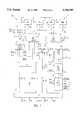
- FIG. 1is a block diagram of a pipeline-burst DRAM (PBDRAM) system in accordance with one embodiment of the present invention
- FIG. 2is a block diagram of memory control sequencer in accordance with one embodiment of the invention.
- FIG. 3is a timing diagram illustrating the operation of the memory control sequencer of FIG. 2;
- FIG. 4is a block diagram illustrating a memory bank, a read buffer, and an I/O device in accordance with one embodiment of the invention
- FIG. 5is a schematic diagram illustrating a bit-slice of the read buffer of FIG. 4;
- FIG. 6is a timing diagram illustrating a pipeline-burst read operation in accordance with one embodiment of the invention.
- FIG. 7is a block diagram of a write buffer in accordance with one embodiment of the invention.
- FIG. 8is a schematic diagram of a bit-slice of a data path within the write buffer of FIG. 7;
- FIG. 9is a schematic diagram of a bit-slice of an address path within the write buffer of FIG. 7;
- FIG. 10is a timing diagram illustrating a pipeline burst write operation in accordance with one embodiment of the invention.
- FIG. 11is a timing diagram illustrating a burst write operation followed by a burst read operation.
- FIG. 12is a timing diagram illustrating a burst read operation followed by a burst write operation.
- FIG. 1is a block diagram of a pipeline-burst DRAM (PBDRAM) system 100 in accordance with one embodiment of the present invention.
- PBDRAM system 100includes I/O device 101, read buffer 102, write buffer 103, memory control sequencer 104, memory operation control circuit 105, write/read buffer control circuit 106, address decoder and latch circuit 107, burst address sequencer 108, address decoder 109 and memory banks 111-114.
- Memory banks 111-114are collectively referred to as memory array 115.
- the elements of memory system 100are fabricated on a single chip.
- Each of memory banks 111-114includes an array of DRAM memory cells having 256 rows and 1024 columns. Each of memory banks 111-114 stores up to 32K words, with 32 bits in each word. Each of memory banks 111-114 further includes a plurality of sense amplifiers, with one sense amplifier coupled to each column of memory cells, and a plurality of word line drivers, with one word line driver coupled to each row of memory cells (i.e., word line). Within each of memory banks 111-114, the sense amplifiers are arranged into groups of eight and connected through 8-to-1 column switches (multiplexers) to 128 pairs of data lines. The column switches, in their off-state, isolate the sense-amplifiers from the data lines. The 128 pairs of data lines form a data bus 116 which is connected in parallel to DRAM banks 111-114, read buffer 102 and write buffer 103.
- I/O deviceis coupled to an external device, such as a microprocessor, to receive a 32-bit data value D 31:0!, a 15-bit address signal A 14:0!, a clock signal CLK, a write/read indicator signal W/R#, an address strobe signal ADS#, and a reset signal RESET.
- I/O device 101is coupled to read buffer 102 and to write buffer 103 by a 32-bit wide data bus 117 which carries the 32-bit data values D 31:0!.
- I/O device 101also provides the upper 13 address bits A 14:2! to address latch circuit 107 and to write buffer 103.
- the lower 2 address bits A 1:0!are provided to burst address sequencer 108. As described in more detail below, address bits A 14:2! are used to address memory banks 111-114, and address bits A 1:0! are used to control the sequence of the data values in a burst operation.
- I/O device 101also provides the address strobe signal ADS#, clock signal CLK and reset signal RESET to memory control sequencer 104. Because the clock signal CLK is provided to most of the elements of memory system 100, for purposes of clarity, the clock signal CLK is not illustrated as entering the various elements of memory system 100. Instead, the clock signal CLK is illustrated as leaving I/O device 101, with the understanding that this clock signal CLK is provided to the elements of memory system 100 as required.
- memory control sequencer 104In response to the received signals, memory control sequencer 104 generates a row access (RAS#) signal and a column access (CAS#) signal. The RAS# and CAS# signals are provided to memory banks 111-114 (not shown). In addition, the RAS# signal is provided to memory operation control circuit 105, and the CAS# signal is provided to write/read buffer control circuit 106.
- RAS#row access
- CAS#column access
- memory operation control circuit 105In response to the RAS# signal, memory operation control circuit 105 generates signals to enable the sense amplifiers and to equalize the bit lines within memory banks 111-114.
- the operation of memory control circuit 105is described in more detail in commonly-owned, U.S. patent application Ser. No. 08/522,032, now U.S. Pat. No. 5,615,169, which is hereby incorporated by reference in its entirety.
- write/read buffer control circuit 106In response to the CAS# signal, write/read buffer control circuit 106 generates a set of read control signals or a set of write control signals, depending on whether I/O device 101 is performing a read operation or a write operation as determined by the W/R# signal.
- Write/read buffer control circuit 106receives the W/R# signal from I/O device 101.
- the state of the W/R# signalindicates whether I/O device 101 is initiating a read or a write transaction.
- a logic high W/R# signalindicates a write transaction, while a logic low W/R# signal indicates a read transaction.
- write/read buffer control circuit 106When I/O device 101 is initiating a read transaction, write/read buffer control circuit 106 generates a data amplifier enable (DA -- EN) signal and a transfer enable (TR) signal to control read buffer 102. Alternatively, when I/O device 101 is initiating a write transaction, write/read buffer control circuit 106 generates a data shift (DSHIFT) signal, an address shift (ASHIFT) signal and a write (WRITE) signal for controlling write buffer 103.
- DSHIFTdata shift
- ASHIFTaddress shift
- WRITEwrite
- FIG. 2is a block diagram of memory control sequencer 104 in accordance with one embodiment of the invention.
- Memory control sequencer 104includes flip-flops 151-154, AND gates 155-156 and NOR gate 157, which are connected as illustrated.
- Memory control sequencer 104generates the RAS# and CAS# signals, which are used to control memory banks 111-114, in response to the ADS#, CLK and RESET signals received from I/O device 101.
- the RAS# and CAS# signalsperform the same functions as conventional row access and column access signals in a conventional DRAM circuit. However, in a conventional DRAM circuit, the row and column access signals are generated off-chip.
- the RAS# signalis provided to memory operation control circuit 105.
- memory operation control circuit 105generates signals to control the following micro-operations within memory arrays 111-114: word line turn-on, sense-amplifier turn-on, column switch turn-on and bit-line equalization.
- Memory operation control circuit 105is described in more detail in commonly owned, U.S. patent application Ser. No. 08/522,032, now U.S. Pat. No. 5,615,169, which is hereby incorporated by reference in its entirety.
- D-type flip-flops 151 and 152 of memory control sequencer 104are connected to form a modulo 3 counter which provides output signals Q1, Q1, Q0, and Q0.
- the output signals Q1, Q0 of this countercount through the sequence: 00, 01, 11.
- the output signals Q0 and Q1,are used as the RAS# and CAS# signals, respectively.
- FIG. 3is a timing diagram illustrating the operation of memory control sequencer 104.
- memory control sequencer 104Prior to clock cycle T1, when no memory access is detected, memory control sequencer 104 is in the idle state "00", and the RAS# and CAS# signals are de-asserted high.
- the transmit (Trs) signal provided by AND gate 156 and the QL signal provided by flip-flop 153are in logic high states.
- I/O circuit 101asserts the ADS# signal by forcing this signal to a logic low state.
- the ADS# signalis provided to the D input of flip flop 154.
- the logic high Trs signal provided to flip flop 154enables the logic low ADS# signal to be passed to the Q output terminal of flip flop 154.
- the logic low ADS# signalis thereby provided to the enable (EN) input terminals of flip flops 151 and 152, thereby enabling these flip flops 151-152 and initiating the counter formed by flip flops 151-152.
- sequencer 104enters the "01" state because the logic high CAS# signal, which is provided to the D input of flip flop 151, is latched into flip flop 151.
- the Q0 output signaltransitions to a logic high state and the RAS# signal (i.e., the Q0 signal) transitions to a logic low state, thereby asserting the RAS# signal.
- the logic high Q0 output signalcauses the output signals provided by NOR gate 157 and AND gate 156 to transition to logic low states.
- the logic low Trs signal provided by AND gate 156prevents subsequent ADS# signals from being latched into flip flop 154 until the current memory access is completed.
- flip flop 153latches the logic low signal provided by NOR gate 157, thereby causing the QL signal to transition to a logic low state.
- the logic low RAS# signalis provided to memory operation control circuit 105.
- memory operation control circuit 104causes memory banks 111-114 to start a RAS cycle.
- the logic low RAS# signalis also provided to address decoder 109.
- address decoder 109decodes the bank address bits A 14:13! to select one of four memory banks 111-114, and decodes the row address bits A 12:5! to select one of the 256 rows within the selected bank.
- the word line of the selected row in the selected bankis asserted high.
- the sense amplifiers of the selected bankare enabled by memory operation control circuit 105.
- memory control sequencer 104transitions to the "11" state as follows.
- the output of AND gate 155is at a logic high state because of the logic high states of the CAS# and Q0 signals.
- the logic high output of AND gate 155is latched into flip flop 152, thereby causing the Q1 output signal to transition to a logic high level and the CAS# signal (i.e., the Q1 signal) to transition to a logic low level. That is, the CAS# signal is asserted low.
- the RAS# signalalso remains asserted low at this time.
- the logic low CAS# signalis provided to memory banks 111-114.
- memory banks 111-114start a CAS cycle.
- the column address bits A 4:2!are decoded to select one of the eight 128-bit word locations within the selected bank, and the column switches associated with this word location are enabled.
- the logic low CAS# signalis also provided to write/read buffer control circuit 106. As described in more detail below, in response to the CAS# signal, write/read buffer control circuit 106 generates signals which are used to control read buffer 102 or write buffer 103.
- memory control sequencer 104transitions back to the "00" idle state as follows.
- the logic low CAS# signalcauses the input signals to both of flip flops 151 and 152 to be logic low values.
- the rising edge of clock cycle T3causes these logic low values to be latched into flip flops 151 and 152, thereby causing the Q0 and Q1 signals to transition to logic low states and the RAS# and CAS# signals to transition to logic high states.
- the logic low Q0 and Q1 signalscause the output signal of NOR gate 157 to transition to a logic high level.
- the logic high output signal provided by NOR gate 157is latched into flip flop 153 at the falling edge of clock cycle T3.
- the QL and Trs signalstransition to logic high states, thereby enabling flip flop 154 to latch a
- memory operation control circuit 105initiates a precharge operation for the selected bank. First, the column switches are turned off. The asserted word line is then turned off. The sense amplifiers are then disabled and equalization of the bit lines are performed. The precharge operation takes approximately one clock cycle (e.g., the duration of clock cycle T3).
- FIG. 4is a block diagram illustrating memory bank 111, read buffer 102 and I/O device 101.
- Memory bank 111includes a 256 ⁇ 1024 array of DRAM memory cells 111a, 1024 sense amplifiers 111b, 128 8-to-1 column select switches 111c, word line driver circuit 111d and bank select circuit 111e.
- Bank select circuit 11eenables memory bank 111 when the bank select signal BS n! is asserted high.
- the BS n!is one of four output signals BS 3:0! provided by address decoder circuit 109 in response to bank address bits A 14:13!.
- Word line driver circuit 111denables one of the 256 word lines in response to the row address bits A 12:5! and the BS n! signal.
- One of the eight groups of 128 column switches in circuit 111cis turned on in response to a column select signal CS 7:0!, the BS n! signal and the CAS# signal.
- the column select CS 7:0! signalis provided by address decoder circuit 109 in response to column select address bits A 4:2!.
- four 32-bit data wordsrepresented by data signals DA 127:0! and complementary data signals DA 127:0!, are provided to read data buffer 102.
- Memory banks 112-114are substantially identical to memory bank 111.
- Read data buffer 102has the capacity to store the 128 bits of data provided by column select switches 111c. Thus, read data buffer 102 is capable of storing all of the data required for a burst transaction involving four 32-bit words in which one word is output per clock cycle.
- Read data buffer 102includes data amplifier circuit 201, transparent latch circuit 202 and 4-to-1 multiplexer 203.
- Data amplifier circuit 201includes 128 data amplifiers, each coupled to receive a corresponding pair of bits from data signal DA 127:0! and complementary data signal DA 127:0!.
- a DA -- EN signal generated by write/read buffer control circuit 106enables data amplifier circuit 201.
- data amplifier circuit 201generates 128 data values representative of four 32-bit words D0 31:0!, D1 31:0!, D2 31:0! and D3 31:0!.
- Transparent latch circuit 202includes 128 data latches, each coupled to receive one of the 128 data values provided by data amplifier circuit 201.
- Transparent latch circuit 202is enabled by a transfer enable signal TR which is generated by write/read buffer control circuit 106, thereby causing the four 32-bit words D0 31:0!, D1 31:0!, D2 31:0! and D3 31:0!, to be latched into transparent latch circuit 202.
- Four-to-one multiplexer 203then sequentially routes these 32-bit words from transparent latch circuit 202 to I/O device 101 in response to a burst access signal BA 1:0! generated by burst access sequencer 108.
- Burst access sequencer 108generates the burst access signals BA 1:0! in response to address signals A 1:0!.
- the predesignated burst sequencecan be in linear or Intel X86 order.
- FIG. 5is a schematic diagram illustrating a bit-slice 204 of read buffer 102.
- Bit-slice 204includes data amplifier 201a and transparent latch 202a.
- Data amplifier 201aincludes p-channel transistors 211-214 and n-channel transistors 215-217.
- P-channel transistors 212-213 and n-channel transistors 215-216are cross-coupled to form a regenerative latch circuit.
- This regenerative latchis enabled and disabled by the DA -- EN signal provided to p-channel transistors 211 and 214 and n-channel transistor 217.
- the regenerative latchWhen enabled by a logic high DA -- EN signal, the regenerative latch amplifies and stores the DA and DA signals present on the pair of data lines connected to data amplifier 201a.
- the amplified DA signalis provided to transparent latch 202a on line 218.
- Transmission gate 224 of transparent latch 202ais connected to line 218 to receive the amplified DA signal from data amplifier 201a.
- Transmission gate 224is controlled by the transfer enable signal TR (and the inverse of the transfer enable signal as created by inverter 221).
- the transfer enable signal TRis received from write/read buffer control circuit 106.
- the transfer enable signal TRis high, transmission gate 224 is turned on and the amplified data signal DA is transferred to the transparent latch 225 formed by inverters 222 and 223.
- the transparent latch 225is isolated from data amplifier 201a. After transparent latch 225 has been isolated from data amplifier 201a, transparent latch 225 stores a data bit corresponding to a current read transaction. At this time, data values for the next (pipelined) read transaction can be stored in data amplifier circuit 201.
- the transfer enable signal TRis pulsed high for one clock cycle, thereby causing the data values for the next read transaction stored in data amplifier 201a to flow directly from data amplifier 201a through transparent latch 202a to I/O circuit 101.
- the data amplifier 201a and the transparent latch 202athus are configured as a double buffer which allows data to be provided without a gap between data values of a current read transaction to data values of the next (pipelined) read transaction.
- the flow-through mechanism which exists between the data amplifier circuit 201 and the I/O device 101eliminates the necessity of a pipeline-stage and the associated increase in read access latency which would be introduced by such a pipeline-stage.
- FIG. 6is a timing diagram illustrating a pipeline-burst read operation in accordance with one embodiment of the invention.
- PBDRAM system 100is idle before cycle T1 of the clock signal CLK.
- cycle T1both the ADS# and W/R# signals are asserted low, and a first read address signal A1 14:0! is driven on the address bus by the microprocessor accessing memory system 100.
- memory control sequencer 104 and write/read buffer control circuit 106detect the arrival of a new read transaction.
- the logic low ADS# signalactivates the memory control sequencer 104 and causes the RAS# signal to be asserted low.
- the logic low ADS# and W/R# signalscause the first read address A1 14:2! to be latched in the address latch circuit 107 and provided to address decoder 109.
- the logic low RAS# signalcauses the appropriate memory bank to be selected in response to address bits A1 14:13! and the appropriate word line to be turned on in response to address bits Al 12:5!. By turning on the word line, the memory cells in the selected row are connected to their respective bit lines.
- the sense-amplifiers in the selected bankare turned on in response to a sense amplifier enable signal generated by memory operation control circuit 105, thereby amplifying the signals on the bit lines.
- the CAS# signalis asserted low by memory control sequencer 104. The logic low CAS# signal causes the column switches selected by the address signals A1 4:2! to turn on, thereby connecting selected sense amplifiers to the data amplifier circuit 201 in read buffer 102.
- the logic low CAS# signalalso causes write/read buffer control circuit 106 to drive the DA -- EN signal to a logic high state, thereby activating the regenerative latches within data amplifier circuit 201.
- the four data values DA0, DA1, DA2 and DA3 required for the entire read burst transactionare thereby prefetched to data amplifier circuit 201 of read buffer 102.
- Write/read buffer control circuit 106also drives the transfer enable signal TR to a logic high state in response to the logic low CAS# signal, thereby latching the data values DA0, DA1, DA2 and DA3 into transparent latch circuit 202.
- Burst address sequencer 108latches address sequence bits A1 1:0! in response to the ADS# signal. Upon receiving the logic high transfer enable signal TR, the burst address sequencer 108 generates a BA 1:0! signal.
- the BA 1:0!has an initial value which is dependent upon the value of address sequence bits A1 1:0!.
- burst access control signal BA 1:0!sequentially transitions according to a predesignated sequence (e.g., a linear sequence or an x86 sequence) defined by address sequence bits A1 1:0!. In the described embodiment, the BA 1:0!
- the BA 1:0! signalis provided to first multiplexer 203, thereby causing the data value D0 to be routed from transparent latch circuit 202 to I/O device 101 through multiplexer 203 during clock cycle T3.
- Data value DA0is provided through multiplexer 203 to I/O device 101 without delay as soon as the transfer enable signal TR is asserted high.
- the burst address sequencer 108generates BA 1:0!
- the data values DA1, DA2 and DA3are routed from transparent latch circuit 202 to I/O device 101 through multiplexer 203 during clock cycles T3, T4 and T5, respectively.
- An additional control signal ADV#can be added to control the advancing of the burst access signal BA 1:0!.
- the burst access signal BA 1:0!is not advanced unless the ADV# signal is asserted.
- the rising edge of clock cycle T4causes the RAS# and CAS# signals to transition to logic high states as previously discussed in connection with FIGS. 2 and 3.
- write/read buffer control circuit 106causes the transfer enable signal TR to transition to a logic low state, thereby isolating transparent latch circuit 202 from data amplifier circuit 201.
- write/read buffer control circuit 106Shortly after the transfer enable signal TR transitions to a logic low state, write/read buffer control circuit 106 causes the DA -- EN signal to transition to a logic low state, thereby precharging the data amplifiers in data amplifier circuit 201.
- memory operation control circuit 105performs a precharge operation on the selected memory bank by turning off the column select switches, turning off the word line driver circuit, turning off the sense amplifier circuit, and precharging the bit lines.
- a subsequent pipeline read transactioncan be initiated during clock cycle T4 by transmitting a logic low ADS# signal, a logic low W/R# signal, and a second address signal A2 14:0! from I/O device 101.
- This pipeline read transactionis detected at the beginning of clock cycle T5.
- the RAS# signalagain goes low at the rising edge of clock cycle T5, initiating another RAS cycle within memory system 100.
- the CAS# signalagain goes low at the rising edge of clock cycle T6, thereby causing write/read buffer control circuit 106 to assert a logic high DA -- EN signal during clock cycle T6.
- a second set of four data values DB0, DB1, DB2 and DB3is thus stored in data amplifier circuit 201 during clock cycle T6.
- the transfer enable signal TRis not asserted during clock cycle T6, such that the data values DA0, DA1, DA2 and DA3, which were stored in transparent latch circuit 202 during the first read transaction, are not disturbed. Only after the last data value DA3 has been read out from transparent latch circuit 202 does the write/read buffer control circuit 106 assert a logic high transfer enable signal TR. The write/read buffer control circuit 106 determines that the last data value DA3 has been read out of transparent latch circuit 202 by monitoring a burst access start signal BST which is generated by the burst address sequencer 108 at the start of each burst transaction. After the transfer enable signal TR has been asserted high, data values DB0, DB1, DB2 and DB3, of the second (pipeline) read transaction, are available to be provided to I/O circuit 101.
- Burst address sequencer 108latches address sequence bits A2 1:0! in response to the ADS# signal at the rising edge of clock cycle T5. Upon receiving the logic high transfer enable signal TR at the rising edge of clock cycle T7, the burst address sequencer 108 generates the BA 1:0! signal in response to the address sequence bits A2 1:0! as previously described and asserts a logic high BST signal to signal the beginning of a new burst sequence.
- the BA 1:0! signalagain has an initial value of 00 and transitions in a linear sequence from "00" to "01" to "10” to "11” in synchronism with the rising edges of the CLK signal.
- first multiplexer 203thereby causing the data values DB0, DB1, DB2 and DB3 to be routed from transparent latch circuit 202 to I/O device 101 through multiplexer 203 during clock cycles T7, T8, T9 and T10, respectively.
- Data value DB0is provided through multiplexer 203 to I/O device 101 without delay as soon as the transfer enable signal TR is asserted high during clock cycle T7.
- the pipeline burst read data transferis therefore gap-less, with data values being provided to I/O device 101 during each of clock cycles T3-T10.
- the address of each read transactioncan be anywhere within the address space spanned by the memory system 100.
- the pipeline read transactionis modified to interrupt the data burst of the first read transaction.
- write/read buffer control circuit 106asserts a logic high transfer enable signal TR at the rising edge of clock cycle T6.
- the first data value DB0 of the second (pipeline) read transactionwill overwrite the last data value DA3 of the first read transaction during clock cycle T6.
- the time at which a current read transaction can be interrupted by a subsequent read transactionis determined mainly by the memory cycle time. When the memory cycle time is equal to 3 clock cycles, a new transaction can be initiated every 3 clock cycles without over-running the memory.
- FIG. 7is a block diagram of write buffer 103, which includes first latch circuit 301, second latch circuit 302 and tri-state buffer circuit 304.
- First latch circuit 301includes a 128-bit wide first data latch 11 and a 13-bit wide first address latch 21.
- second latch circuit 302includes a 128-bit wide second data latch 12 and a 13-bit wide second address latch 22.
- Tri-state buffer circuit 304includes 128 tri-state data buffers 13 and 13 tri-state address buffers 23.
- First data latch 11is partitioned into four registers 11a, 11b, 11c and 11d, with each register storing 32-bits. Each of these four registers 11a-11d is connected in parallel to receive the data value D 31:0! from the data bus. First data latch 11 also receives a 4-bit data latch signal DLAT 3:0! from burst address sequencer 108. Each of the four bits of the DLAT 3:0! signal activates a corresponding one of the four registers 11a-11d, thereby latching the data value D 31:0! into the activated register.
- First address latch 21is also connected to receive address signals A 14:2! from I/O device 101. Address signals A 14:2! are latched into first address latch 21 in response to a WRITE signal received from write/read buffer control circuit 106.
- Second data latch 12is coupled to receive the four 32-bit words stored in the first data latch 11. The contents of the first data latch 11 are latched into the second data latch 12 in response to a data shift (DSHIFT) signal received from write/read buffer control circuit 106.
- Second address latch 22is connected to receive address signals A 14:2! stored in the first address latch 21. The contents of the first address latch 21 are latched into the second address latch 22 in response to an address shift (ASHIFT) signal received from write/read buffer control circuit 106.
- DSHIFTdata shift
- Second address latch 22is connected to receive address signals A 14:2! stored in the first address latch 21. The contents of the first address latch 21 are latched into the second address latch 22 in response to an address shift (ASHIFT) signal received from write/read buffer control circuit 106.
- ASHIFTaddress shift
- the tri-state data buffers 13are connected to receive the contents of second data latch 12, and the tri-state address buffers 23 are connected to receive the contents of second address latch 22.
- the contents of the second data latch 12 and the second address latch 22are routed through the tri-state data buffers 13 and the tri-state address buffers 23, respectively, in response to the WRITE signal provided by the write/read buffer control circuit 106.
- the first and second data latches 11 and 12each have the capacity to store all of the data values required for a burst of four 32-bit data values.
- Address buffers 21 and 22store the addresses corresponding to the data values stored in data buffers 11 and 12, respectively.
- the first and second latch circuits 301 and 302are configured to form a 2-deep first in, first out (FIFO) memory.
- the first data latch 11is dedicated for storing data values of a current write transaction
- the second data latch 12is dedicated for storing data values of a previous write transaction which are currently being retired to a selected one of memory banks 111-114.
- FIG. 8is a schematic diagram of the nth bit-slice 311 of first data latch 11, second data latch 12 and tri-state data buffer 13.
- Bit-slice 311includes a data latch 11n and a data latch 12n which are connected in cascade to form a two-bit shift register.
- Data latch 11nis coupled to receive data bit D n! of data value D 31:0! and data latch signal DLAT x!.
- Data latch signal DLAT x!is one of the four DLAT 3:0! signals.
- the 32 data latches which form register 11aare connected to receive DLAT 0!
- the 32 data latches which form register 11bare connected to receive DLAT 1!
- the 32 data latches which form register 11care connected to receive DLAT 2!
- the 32 data latches which form register 11dare connected to receive DLAT 3!.
- Data latch 12nis coupled to receive data bit D n! from data latch 11n. Data latch 12n latches in data bit D n! when the DSHIFT signal is asserted high. Tri-state buffer 13n is coupled to receive data bit D n! from data latch 12n. When the WRITE signal is asserted high, tri-state buffer 13n transmits the data bit D n! as data signal DA n! and transmits the inverse of data bit D n! as data signal DA n! to memory banks 111-114.
- FIG. 9is a schematic diagram of the mth bit-slice 312 of first address latch 21, second address latch 22 and tri-state address buffer 23.
- Bit-slice 312includes an address latch 21m and an address latch 22m which are connected in cascade to form a two-bit shift register.
- Address latch 21mis coupled to receive address bit A m! and the WRITE signal. When the WRITE signal is asserted high, address bit A m! is latched into address latch 21m.
- Address latch 22mis coupled to receive address bit A m! from address latch 21m. Address latch 22m latches in address bit A m! when the ASHIFT signal is asserted high. Tri-state buffer 23m is coupled to receive address bit A m! from address latch 22m. When the WRITE signal is asserted high, tri-state buffer 23m transmits the address bit A m! to address decoder 109.
- FIG. 10is a timing diagram illustrating a pipeline burst write operation in accordance with one embodiment of the invention.
- Memory system 100is in an idle state before cycle T1 of clock signal CLK.
- a microprocessor(not shown) coupled to I/O device 101 begins a first write transaction by driving a first memory address A1 14:0! onto the address bus, driving the W/R# signal to a logic high state, driving the ADS# signal to a logic low state and driving a first data signal DA0 31:0! onto the data bus 117.
- These signalsare buffered by I/O device 101.
- Memory control sequencer 104detects the write transaction at the rising edge of clock cycle T2 in the manner previously described in connection with FIGS. 2 and 3.
- the memory control sequencer 104In response to the logic low ADS# signal, the memory control sequencer 104 generates a logic low RAS# signal.
- the logic low RAS# signalcauses the write/read buffer control circuit 106 to generate a logic high WRITE signal.
- This logic high WRITE signalis provided to the first address latch 21, thereby causing the first address signal A1 14:2! to be written to first address latch 21.
- Burst address sequencer 108latches address sequence bits A1 1:0! in response to the ADS# signal. Upon receiving the logic high WRITE signal, the burst address sequencer 108 generates a DLAT 3:0! signal.
- the DLAT 3:0!has an initial value which is dependent upon the value of address sequence bits A1 1:0!. In the described embodiment, the DLAT 3:0! signal has an initial value of 0001.
- This DLAT 3:0! signalis provided to first data latch 11, thereby causing the data value DAO 31:0! to be written to the first register 11a within first data latch 11 during clock cycle T2.
- the I/O device 101drives second, third and fourth data signals DA1 31:0!, DA2 3:0! and DA3 3:0!, respectively, onto the data bus 117.
- burst address sequencer 108generates DLAT 3:0! signals having predesignated values (e.g., 0010, 0100 and 1000, respectively), which are determined by the address sequence bits A1 1:0!.
- the data values DA1 31:0!, DA2 3:0! and DA3 3:0!are written to corresponding registers (e.g., registers 11b, 11c and 11d, respectively), within first data latch 11 during clock cycles T3, T4 and T5.
- memory control sequencer 104causes the CAS# signal to be asserted low at the rising edge of clock cycle T3. At the rising edge of clock cycle T4, memory control sequencer 104 causes the RAS# and CAS# signals to be de-asserted high. In response to the de-asserted RAS# and CAS# signals, the write/read buffer control circuit 106 de-asserts the WRITE signal low. The low WRITE signal turns off tri-state buffer circuit 310, thereby isolating the selected memory bank from write buffer 103.
- the write/read buffer control circuit 106asserts logic high ASHIFT and DSHIFT signals.
- the ASHIFT and DSHIFT signalsremain asserted until the next write transaction is initiated (i.e., until write/read buffer control circuit receives another logic low RAS# signal).
- the logic high DSHIFT signalis applied to second data latch 12, thereby causing the data values DA0, DA1, DA2 and DA3 to be latched into second data latch 12.
- the logic high ASHIFT signalis applied to the second address latch 22, thereby causing the first address signals A1 14:2! to be latched into second address latch 22.
- the first set of data values DA0, DA1, DA2 and DA3is not written to the memory array 115 during the first write transaction. Rather, the first set of data values is stored in the second latch circuit 302 until the second write transaction is initiated. When the second write transaction is initiated, the first set of data values is written to the memory array 115 as described below.
- the microprocessor coupled to I/O device 101begins a second write transaction by driving a second memory address A2 14:0! onto the address bus, driving the W/R# signal to a logic high state, driving the ADS# signal to a logic low state and driving the data signal DB0 31:0! onto the data bus 117. Again, I/O device 101 buffers these signals.
- Memory control sequencer 104detects the write transaction at the rising edge of clock cycle T6 in the manner previously described in connection with FIGS. 2 and 3. In response to the logic low ADS# signal, the memory control sequencer 104 generates a logic low RAS# signal. The logic low RAS# signal further causes write/read buffer control circuit 106 to generate a logic high WRITE signal.
- This logic high WRITE signalis provided to the first address latch 21, thereby causing a second address signal A2 14:2! to be written to first address latch 21.
- the logic high WRITE signalalso causes tri-state data buffer 13 to pass data values DA0, DA1, DA2 and DA3 from second data latch 12 to memory banks 111-114.
- the logic high WRITE signalfurther causes tri-state address buffer 23 to pass the first address signal A1 14:2! is latched into address decoder 109 by the logic low RAS# signal. In response, address decoder 109 enables the selected memory bank and word line.
- Burst address sequencer 108latches address sequence bits A2 1:0! in response to the ADS# signal. In response to the logic high WRITE signal, the burst address sequencer 108 sequentially generates DLAT 3:0! signals having values depending on the values of A 1:0! and the predesignated burst sequence. These DLAT 3:0! signals are provided to first data latch 11, along with data values DB0, DB1, DB2 and DB3, thereby causing data values DB0, DB1, DB2 and DB3 to be written to corresponding registers 11a, 11b, 11c and 11d of first data latch 11 during clock cycles T6, T7, T8 and T9, respectively.
- Memory control sequencer 104causes the CAS# signal to be asserted low at the rising edge of clock cycle T7. In response, the selected memory bank enters a CAS cycle. The logic low CAS# signal causes selected column switches to turn on. As a result, the data values DA0, DA1, DA2 and DA3 are written to the address identified by address signal A1 14:2!.
- Memory control sequencer 104causes the RAS# and CAS# signals to be de-asserted high at the rising edge of clock cycle T8.
- the write/read buffer control circuit 106de-asserts the WRITE signal and asserts logic high DSHIFT and ASHIFT signals.
- the logic low WRITE signalturns off tri-state buffer circuit 310, thereby isolating the memory array 115 from write buffer 103.
- memory arraygoes through the precharge operation as previously described.
- the DSHIFT and ASHIFT signalsremain asserted until the next write transaction is initiated (i.e., until write/read buffer control circuit receives another logic low RAS# signal).
- the logic high DSHIFT signalis applied to second data latch 12, thereby causing the data values DB0, DB1, DB2 and DB3 to be latched into second data latch 12.
- the logic high ASHIFT signalis applied to the second address latch 22, thereby causing the address A2 14:2! to be latched in address latch 22.
- the second set of data values DB0, DB1, DB2 and DB3 and the second address A2 14:2!are therefore stored for when the third write transaction is initiated.
- the first set of data values DA0, DA1, DA2 and DA3are retired to the memory array, while the second set of data values DB0, DB1, DB2 and DB3 and the second address A2 14:2! are latched into second latch circuit 302. Consequently, the data pipeline burst transfer can be gap-less, with data values being written to memory device 100 during each clock cycle.
- the address of each write transactioncan be anywhere within the address space spanned by the memory system 100.
- the previous descriptionhas described a first burst read operation pipelined with a second burst read operation.
- the previous descriptionhas also described a first burst write operation pipelined with a second burst write operation.
- memory system 100also facilitates a burst read operation pipelined with a subsequent burst write operation, and (2) a burst write operation pipelined with a subsequent burst read operation.
- FIG. 11is a timing diagram illustrating a burst write operation followed by a burst read operation.
- the burst write operationis initiated at the rising edge of clock cycle T2 and proceeds as previously described in connection with FIG. 10. Not all of the waveforms associated with this burst write operation are shown in FIG. 11, as these waveforms were previously discussed in connection with FIG. 10.
- the burst read operationis initiated at the rising edge of clock cycle T5 and proceeds as previously described in connection with FIG. 6. Not all of the waveforms associated with this burst read operation are shown in FIG. 11, as these waveforms were previously discussed in connection with FIG. 6.
- the dead time between the burst write and burst read transactionsis minimized to one clock cycle. This dead clock cycle enables the direction of data flow on the data bus to be reversed for the burst read operation.
- FIG. 12is a timing diagram illustrating a burst read operation followed by a burst write operation.
- the burst read operationis initiated at the rising edge of clock cycle T2 and proceeds as previously described in connection with FIG. 6. Not all of the waveforms associated with this burst write operation are shown in FIG. 12, as these waveforms were previously discussed in connection with FIG. 6.
- the burst write operationis initiated at the rising edge of clock cycle T9 and proceeds as previously described in connection with FIG. 10. Not all of the waveforms associated with this burst write operation are shown in FIG. 12, as these waveforms were previously discussed in connection with FIG. 10.
- the burst write transactionis not initiated until the rising edge of clock cycle T9 to provide a dead clock cycle between the burst read and burst write transactions. This dead clock cycle enables the direction of data flow on the data bus to be reversed for the burst write operation.
Landscapes
- Dram (AREA)
Abstract
Description
Claims (28)
Priority Applications (1)
| Application Number | Priority Date | Filing Date | Title |
|---|---|---|---|
| US08/679,873US5784705A (en) | 1996-07-15 | 1996-07-15 | Method and structure for performing pipeline burst accesses in a semiconductor memory |
Applications Claiming Priority (1)
| Application Number | Priority Date | Filing Date | Title |
|---|---|---|---|
| US08/679,873US5784705A (en) | 1996-07-15 | 1996-07-15 | Method and structure for performing pipeline burst accesses in a semiconductor memory |
Publications (1)
| Publication Number | Publication Date |
|---|---|
| US5784705Atrue US5784705A (en) | 1998-07-21 |
Family
ID=24728723
Family Applications (1)
| Application Number | Title | Priority Date | Filing Date |
|---|---|---|---|
| US08/679,873Expired - LifetimeUS5784705A (en) | 1996-07-15 | 1996-07-15 | Method and structure for performing pipeline burst accesses in a semiconductor memory |
Country Status (1)
| Country | Link |
|---|---|
| US (1) | US5784705A (en) |
Cited By (60)
| Publication number | Priority date | Publication date | Assignee | Title |
|---|---|---|---|---|
| US5901086A (en)* | 1996-12-26 | 1999-05-04 | Motorola, Inc. | Pipelined fast-access floating gate memory architecture and method of operation |
| US6011745A (en)* | 1997-07-31 | 2000-01-04 | Nec Corporation | Semiconductor memory system with bank switching control |
| EP0978842A1 (en)* | 1998-08-04 | 2000-02-09 | Samsung Electronics Co., Ltd. | Synchronous burst semiconductor memory device |
| US6075740A (en)* | 1998-10-27 | 2000-06-13 | Monolithic System Technology, Inc. | Method and apparatus for increasing the time available for refresh for 1-t SRAM compatible devices |
| EP1028427A1 (en)* | 1999-02-11 | 2000-08-16 | Infineon Technologies North America Corp. | Hierarchical prefetch for semiconductor memories |
| EP1035548A1 (en)* | 1999-03-08 | 2000-09-13 | Kabushiki Kaisha Toshiba | Synchronous semiconductor memory device |
| US6163832A (en)* | 1996-02-02 | 2000-12-19 | Fujitsu Limited | Semiconductor memory device including plural blocks with a pipeline operation for carrying out operations in predetermined order |
| US6198682B1 (en) | 1999-02-13 | 2001-03-06 | Integrated Device Technology, Inc. | Hierarchical dynamic memory array architecture using read amplifiers separate from bit line sense amplifiers |
| EP1103978A1 (en)* | 1999-11-25 | 2001-05-30 | STMicroelectronics S.r.l. | Non-volatile memory device with burst mode reading and corresponding reading method |
| EP1103977A1 (en)* | 1999-11-25 | 2001-05-30 | STMicroelectronics S.r.l. | Method for reading data from a non-volatile memory device with autodetect burst mode reading and corresponding reading circuit |
| US6259646B1 (en)* | 2000-01-28 | 2001-07-10 | Micron Technology, Inc. | Fast accessing of a memory device |
| WO2001020611A3 (en)* | 1999-09-14 | 2001-08-02 | Terry L Kendall | Controlling burst sequence in synchronous memories |
| US6356485B1 (en) | 1999-02-13 | 2002-03-12 | Integrated Device Technology, Inc. | Merging write cycles by comparing at least a portion of the respective write cycle addresses |
| US6392935B1 (en)* | 2000-04-03 | 2002-05-21 | Maxtor Corporation | Maximum bandwidth/minimum latency SDRAM interface |
| US6415353B1 (en) | 1998-10-01 | 2002-07-02 | Monolithic System Technology, Inc. | Read/write buffers for complete hiding of the refresh of a semiconductor memory and method of operating same |
| EP1220225A1 (en)* | 2000-12-28 | 2002-07-03 | STMicroelectronics S.r.l. | Method and device for reducing the mean access time to a non volatile memory during the reading phase |
| US6449685B1 (en) | 1998-10-01 | 2002-09-10 | Monolithic System Technology, Inc. | Read/write buffers for complete hiding of the refresh of a semiconductor memory and method of operating same |
| US6505259B1 (en)* | 1999-08-27 | 2003-01-07 | Intel Corporation | Reordering of burst data transfers across a host bridge |
| US6515916B2 (en)* | 2000-01-26 | 2003-02-04 | Sony Corporation | Column switch in memory device and cache memory using the same |
| US20030039163A1 (en)* | 1998-10-01 | 2003-02-27 | Monolithic System Technology, Inc. | Method and apparatus for completely hiding refresh operations in a DRAM device using clock division |
| US6539454B2 (en)* | 1998-04-01 | 2003-03-25 | Mosaid Technologies Incorporated | Semiconductor memory asynchronous pipeline |
| US20030097535A1 (en)* | 1995-05-17 | 2003-05-22 | Fu-Chieh Hsu | High speed memory system |
| US6587388B2 (en) | 2001-04-27 | 2003-07-01 | International Business Machines Corporation | Method and apparatus for reducing write operation time in dynamic random access memories |
| EP1132925A3 (en)* | 2000-02-25 | 2003-08-13 | Infineon Technologies North America Corp. | Data path calibration and testing mode using a data bus for semiconductor memories |
| US6622224B1 (en)* | 1997-12-29 | 2003-09-16 | Micron Technology, Inc. | Internal buffered bus for a drum |
| US6625077B2 (en) | 2001-10-11 | 2003-09-23 | Cascade Semiconductor Corporation | Asynchronous hidden refresh of semiconductor memory |
| WO2003007303A3 (en)* | 2001-07-13 | 2003-11-06 | Micron Technology Inc | Memory device having different burst order addressing for read and write operations |
| US20040047228A1 (en)* | 2001-10-11 | 2004-03-11 | Cascade Semiconductor Corporation | Asynchronous hidden refresh of semiconductor memory |
| US6707743B2 (en) | 1998-10-01 | 2004-03-16 | Monolithic System Technology, Inc. | Method and apparatus for completely hiding refresh operations in a DRAM device using multiple clock division |
| US20040119139A1 (en)* | 2002-12-24 | 2004-06-24 | Takehiko Hojo | Semiconductor device having a redundancy function |
| US6772312B2 (en) | 1998-04-01 | 2004-08-03 | Mosaid Technologies Incorporated | Semiconductor memory having asynchronous pipeline stages |
| US20040162935A1 (en)* | 2001-12-07 | 2004-08-19 | Janzen Jeffery W. | Sequential nibble burst ordering for data |
| US6782435B2 (en) | 2001-03-26 | 2004-08-24 | Intel Corporation | Device for spatially and temporally reordering for data between a processor, memory and peripherals |
| US20040170079A1 (en)* | 2003-02-28 | 2004-09-02 | Wingyu Leung | Method and apparatus for lengthening the data-retention time of a dram device in standby mode |
| US6795341B2 (en)* | 2001-06-15 | 2004-09-21 | Infineon Technologies Ag | Circuit arrangement for the storage of digital data |
| US20040202036A1 (en)* | 2000-07-07 | 2004-10-14 | Paul Demone | High speed DRAM architecture with uniform access latency |
| US6829682B2 (en) | 2001-04-26 | 2004-12-07 | International Business Machines Corporation | Destructive read architecture for dynamic random access memories |
| US20050086420A1 (en)* | 2002-04-25 | 2005-04-21 | Wilcox Jeffrey R. | Low latency buffer control system and method |
| US6898140B2 (en) | 1998-10-01 | 2005-05-24 | Monolithic System Technology, Inc. | Method and apparatus for temperature adaptive refresh in 1T-SRAM compatible memory using the subthreshold characteristics of MOSFET transistors |
| US20060089625A1 (en)* | 2004-10-22 | 2006-04-27 | Voegele James W | System and method for treatment of tissue using the tissue as a fiducial |
| US20060168418A1 (en)* | 2005-01-25 | 2006-07-27 | Adusumilli Vijaya P | Simultaneous pipelined read with dual level cache for improved system performance using flash technology |
| US7149916B1 (en)* | 2003-03-17 | 2006-12-12 | Network Equipment Technologies, Inc. | Method for time-domain synchronization across a bit-sliced data path design |
| US20060291321A1 (en)* | 2005-06-24 | 2006-12-28 | Monolithic System Technology, Inc. | Word line driver for DRAM embedded in a logic process |
| EP1326257B1 (en)* | 2001-12-21 | 2010-04-14 | Fujitsu Microelectronics Limited | Pipelined programming for a NAND type flash memory |
| US20100226176A1 (en)* | 2005-04-01 | 2010-09-09 | Yan Li | Method for Non-Volatile Memory With Background Data Latch Caching During Read Operations |
| US20110016269A1 (en)* | 2009-07-16 | 2011-01-20 | Hyun Lee | System and method of increasing addressable memory space on a memory board |
| US20110016250A1 (en)* | 2009-07-16 | 2011-01-20 | Netlist, Inc. | System and method utilizing distributed byte-wise buffers on a memory module |
| DE19943176B4 (en)* | 1998-09-18 | 2012-09-20 | National Semiconductor Corp.(N.D.Ges.D.Staates Delaware) | Memory controller for controlling an SDRAM in a network switch |
| US8374051B2 (en) | 2011-03-03 | 2013-02-12 | Sandisk 3D Llc | Three dimensional memory system with column pipeline |
| US8472280B2 (en) | 2010-12-21 | 2013-06-25 | Sandisk Technologies Inc. | Alternate page by page programming scheme |
| US8516188B1 (en) | 2004-03-05 | 2013-08-20 | Netlist, Inc. | Circuit for memory module |
| US8553476B2 (en) | 2011-03-03 | 2013-10-08 | Sandisk 3D Llc | Three dimensional memory system with page of data across word lines |
| CN103514124A (en)* | 2012-06-14 | 2014-01-15 | 国际商业机器公司 | Reducing store operation busy times |
| US8756364B1 (en) | 2004-03-05 | 2014-06-17 | Netlist, Inc. | Multirank DDR memory modual with load reduction |
| US8782350B2 (en) | 2008-04-14 | 2014-07-15 | Netlist, Inc. | Circuit providing load isolation and noise reduction |
| US8990489B2 (en) | 2004-01-05 | 2015-03-24 | Smart Modular Technologies, Inc. | Multi-rank memory module that emulates a memory module having a different number of ranks |
| US9053766B2 (en) | 2011-03-03 | 2015-06-09 | Sandisk 3D, Llc | Three dimensional memory system with intelligent select circuit |
| US9128632B2 (en) | 2009-07-16 | 2015-09-08 | Netlist, Inc. | Memory module with distributed data buffers and method of operation |
| US9318160B2 (en) | 2010-11-03 | 2016-04-19 | Netlist, Inc. | Memory package with optimized driver load and method of operation |
| US10324841B2 (en) | 2013-07-27 | 2019-06-18 | Netlist, Inc. | Memory module with local synchronization |
Citations (10)
| Publication number | Priority date | Publication date | Assignee | Title |
|---|---|---|---|---|
| US5289584A (en)* | 1991-06-21 | 1994-02-22 | Compaq Computer Corp. | Memory system with FIFO data input |
| US5402389A (en)* | 1994-03-08 | 1995-03-28 | Motorola, Inc. | Synchronous memory having parallel output data paths |
| US5469558A (en)* | 1991-08-16 | 1995-11-21 | Multichip Technology | Dynamically reconfigurable memory system with programmable controller and FIFO buffered data channels |
| US5502835A (en)* | 1994-08-31 | 1996-03-26 | Motorola, Inc. | Method for synchronously accessing memory |
| US5513148A (en)* | 1994-12-01 | 1996-04-30 | Micron Technology Inc. | Synchronous NAND DRAM architecture |
| US5519839A (en)* | 1992-10-02 | 1996-05-21 | Compaq Computer Corp. | Double buffering operations between the memory bus and the expansion bus of a computer system |
| US5519847A (en)* | 1993-06-30 | 1996-05-21 | Intel Corporation | Method of pipelining sequential writes in a flash memory |
| US5579267A (en)* | 1994-09-28 | 1996-11-26 | Nec Corporation | Semiconductor pipeline memory device eliminating time loss due to difference between pipeline stages from data access |
| US5586282A (en)* | 1990-08-24 | 1996-12-17 | Fujitsu Limited | Memory system employing pipeline process for accessing memory banks |
| US5592435A (en)* | 1994-06-03 | 1997-01-07 | Intel Corporation | Pipelined read architecture for memory |
- 1996
- 1996-07-15USUS08/679,873patent/US5784705A/ennot_activeExpired - Lifetime
Patent Citations (10)
| Publication number | Priority date | Publication date | Assignee | Title |
|---|---|---|---|---|
| US5586282A (en)* | 1990-08-24 | 1996-12-17 | Fujitsu Limited | Memory system employing pipeline process for accessing memory banks |
| US5289584A (en)* | 1991-06-21 | 1994-02-22 | Compaq Computer Corp. | Memory system with FIFO data input |
| US5469558A (en)* | 1991-08-16 | 1995-11-21 | Multichip Technology | Dynamically reconfigurable memory system with programmable controller and FIFO buffered data channels |
| US5519839A (en)* | 1992-10-02 | 1996-05-21 | Compaq Computer Corp. | Double buffering operations between the memory bus and the expansion bus of a computer system |
| US5519847A (en)* | 1993-06-30 | 1996-05-21 | Intel Corporation | Method of pipelining sequential writes in a flash memory |
| US5402389A (en)* | 1994-03-08 | 1995-03-28 | Motorola, Inc. | Synchronous memory having parallel output data paths |
| US5592435A (en)* | 1994-06-03 | 1997-01-07 | Intel Corporation | Pipelined read architecture for memory |
| US5502835A (en)* | 1994-08-31 | 1996-03-26 | Motorola, Inc. | Method for synchronously accessing memory |
| US5579267A (en)* | 1994-09-28 | 1996-11-26 | Nec Corporation | Semiconductor pipeline memory device eliminating time loss due to difference between pipeline stages from data access |
| US5513148A (en)* | 1994-12-01 | 1996-04-30 | Micron Technology Inc. | Synchronous NAND DRAM architecture |
Non-Patent Citations (8)
| Title |
|---|
| Bondurant, David, "15nsec Enhanced DRAM Upgrades System Performance in 72-Pin SIMM Socket," Silicon Valley Personal Computer Design Conference Proceedings (date of publication unknown), pp. 81-86. |
| Bondurant, David, 15nsec Enhanced DRAM Upgrades System Performance in 72 Pin SIMM Socket, Silicon Valley Personal Computer Design Conference Proceedings (date of publication unknown), pp. 81 86.* |
| Dosaka et al., "A 100-MHz 4-Mb Cache DRAM with Fast Copy-Back Scheme," IEEE Journal of Solid-State Circuits, vol. 27, No. 11, Nov. 1992, pp. 1534-1539. |
| Dosaka et al., A 100 MHz 4 Mb Cache DRAM with Fast Copy Back Scheme, IEEE Journal of Solid State Circuits, vol. 27, No. 11, Nov. 1992, pp. 1534 1539.* |
| Intel, "Pentium Processor 3.3V Pipelined BSRAM Specification," Ver. 2.0, May 25, 1995, pp. 1-44. |
| Intel, Pentium Processor 3.3V Pipelined BSRAM Specification, Ver. 2.0, May 25, 1995, pp. 1 44.* |
| Sunaga et al., "A Full bit Prefetch Architecture for Synchronous DRAM's," IEEE Journal of Solid-State Circuits, vol. 30, No. 9, Sep. 1995, pp. 998-1005. |
| Sunaga et al., A Full bit Prefetch Architecture for Synchronous DRAM s, IEEE Journal of Solid State Circuits, vol. 30, No. 9, Sep. 1995, pp. 998 1005.* |
Cited By (146)
| Publication number | Priority date | Publication date | Assignee | Title |
|---|---|---|---|---|
| US20030097535A1 (en)* | 1995-05-17 | 2003-05-22 | Fu-Chieh Hsu | High speed memory system |
| US7206913B2 (en)* | 1995-05-17 | 2007-04-17 | Monolithic System Technology, Inc. | High speed memory system |
| US20050027929A1 (en)* | 1995-05-17 | 2005-02-03 | Monolithic System Technology, Inc. | High speed memory system |
| US6507900B1 (en) | 1996-02-02 | 2003-01-14 | Fujitsu Limited | Semiconductor memory device including plural blocks with selecting and sensing or reading operations in different blocks carried out in parallel |
| US6163832A (en)* | 1996-02-02 | 2000-12-19 | Fujitsu Limited | Semiconductor memory device including plural blocks with a pipeline operation for carrying out operations in predetermined order |
| US6011719A (en)* | 1996-12-26 | 2000-01-04 | Motorola, Inc. | Digital signal processor having an on-chip pipelined EEPROM data memory and a on-chip pipelined EEPROM program memory |
| US5901086A (en)* | 1996-12-26 | 1999-05-04 | Motorola, Inc. | Pipelined fast-access floating gate memory architecture and method of operation |
| US6011745A (en)* | 1997-07-31 | 2000-01-04 | Nec Corporation | Semiconductor memory system with bank switching control |
| US6622224B1 (en)* | 1997-12-29 | 2003-09-16 | Micron Technology, Inc. | Internal buffered bus for a drum |
| US20050033899A1 (en)* | 1998-01-04 | 2005-02-10 | Mosaid Technologies Incorporated | Semiconductor memory asynchronous pipeline |
| US6772312B2 (en) | 1998-04-01 | 2004-08-03 | Mosaid Technologies Incorporated | Semiconductor memory having asynchronous pipeline stages |
| US9548088B2 (en) | 1998-04-01 | 2017-01-17 | Conversant Intellectual Property Management Inc. | Semiconductor memory asynchronous pipeline |
| US8122218B2 (en) | 1998-04-01 | 2012-02-21 | Mosaid Technologies Incorporated | Semiconductor memory asynchronous pipeline |
| US7509469B2 (en) | 1998-04-01 | 2009-03-24 | Mosaid Technologies Incorporated | Semiconductor memory asynchronous pipeline |
| US20100217928A1 (en)* | 1998-04-01 | 2010-08-26 | Ian Mes | Semiconductor Memory Asynchronous Pipeline |
| US20070186034A1 (en)* | 1998-04-01 | 2007-08-09 | Mosaid Technologies Incorporated | Semiconductor memory asynchronous pipeline |
| US8601231B2 (en) | 1998-04-01 | 2013-12-03 | Mosaid Technologies Incorporated | Semiconductor memory asynchronous pipeline |
| US8078821B2 (en) | 1998-04-01 | 2011-12-13 | Mosaid Technologies Incorporated | Semiconductor memory asynchronous pipeline |
| US6539454B2 (en)* | 1998-04-01 | 2003-03-25 | Mosaid Technologies Incorporated | Semiconductor memory asynchronous pipeline |
| US20110202713A1 (en)* | 1998-04-01 | 2011-08-18 | Mosaid Technologies Incorporated | Semiconductor Memory Asynchronous Pipeline |
| US7178001B2 (en) | 1998-04-01 | 2007-02-13 | Mosaid Technologies Inc. | Semiconductor memory asynchronous pipeline |
| US20090175103A1 (en)* | 1998-04-01 | 2009-07-09 | Mosaid Technologies Incorporated | Semiconductor memory asynchronous pipeline |
| US7865685B2 (en) | 1998-04-01 | 2011-01-04 | Mosaid Technologies Incorporated | Semiconductor memory asynchronous pipeline |
| CN1326150C (en)* | 1998-08-04 | 2007-07-11 | 三星电子株式会社 | Synchronous random semiconductor memory |
| EP0978842A1 (en)* | 1998-08-04 | 2000-02-09 | Samsung Electronics Co., Ltd. | Synchronous burst semiconductor memory device |
| DE19943176B4 (en)* | 1998-09-18 | 2012-09-20 | National Semiconductor Corp.(N.D.Ges.D.Staates Delaware) | Memory controller for controlling an SDRAM in a network switch |
| US6449685B1 (en) | 1998-10-01 | 2002-09-10 | Monolithic System Technology, Inc. | Read/write buffers for complete hiding of the refresh of a semiconductor memory and method of operating same |
| US6898140B2 (en) | 1998-10-01 | 2005-05-24 | Monolithic System Technology, Inc. | Method and apparatus for temperature adaptive refresh in 1T-SRAM compatible memory using the subthreshold characteristics of MOSFET transistors |
| US20030039163A1 (en)* | 1998-10-01 | 2003-02-27 | Monolithic System Technology, Inc. | Method and apparatus for completely hiding refresh operations in a DRAM device using clock division |
| US6415353B1 (en) | 1998-10-01 | 2002-07-02 | Monolithic System Technology, Inc. | Read/write buffers for complete hiding of the refresh of a semiconductor memory and method of operating same |
| US6707743B2 (en) | 1998-10-01 | 2004-03-16 | Monolithic System Technology, Inc. | Method and apparatus for completely hiding refresh operations in a DRAM device using multiple clock division |
| US6075740A (en)* | 1998-10-27 | 2000-06-13 | Monolithic System Technology, Inc. | Method and apparatus for increasing the time available for refresh for 1-t SRAM compatible devices |
| US6256248B1 (en) | 1998-10-27 | 2001-07-03 | Monolithic System Technology, Inc. | Method and apparatus for increasing the time available for internal refresh for 1-T SRAM compatible devices |
| EP1028427A1 (en)* | 1999-02-11 | 2000-08-16 | Infineon Technologies North America Corp. | Hierarchical prefetch for semiconductor memories |
| US20050166009A1 (en)* | 1999-02-13 | 2005-07-28 | Proebsting Robert J. | Integrated circuit random access memory capable of automatic internal refresh of memory array |
| US9117541B2 (en) | 1999-02-13 | 2015-08-25 | Intellectual Ventures I Llc | Refresh request queuing circuitry |
| US8417883B2 (en) | 1999-02-13 | 2013-04-09 | Intellectual Ventures I Llc | Concurrent memory bank access and refresh request queuing |
| US10049716B2 (en) | 1999-02-13 | 2018-08-14 | Intellectual Ventures I Llc | Refresh request queuing circuitry |
| US6198682B1 (en) | 1999-02-13 | 2001-03-06 | Integrated Device Technology, Inc. | Hierarchical dynamic memory array architecture using read amplifiers separate from bit line sense amplifiers |
| US7640391B2 (en) | 1999-02-13 | 2009-12-29 | Robert J Proebsting | Integrated circuit random access memory capable of automatic internal refresh of memory array |
| US8151044B2 (en) | 1999-02-13 | 2012-04-03 | Intellectual Ventures I Llc | Concurrent memory bank access and refresh retirement |
| US20100095058A1 (en)* | 1999-02-13 | 2010-04-15 | Proebsting Robert J | Integrated circuit random access memory capable of automatic internal refresh of memory array |
| US6356485B1 (en) | 1999-02-13 | 2002-03-12 | Integrated Device Technology, Inc. | Merging write cycles by comparing at least a portion of the respective write cycle addresses |
| US6163501A (en)* | 1999-03-08 | 2000-12-19 | Kabushiki Kaisha Toshiba | Synchronous semiconductor memory device |
| EP1035548A1 (en)* | 1999-03-08 | 2000-09-13 | Kabushiki Kaisha Toshiba | Synchronous semiconductor memory device |
| US6505259B1 (en)* | 1999-08-27 | 2003-01-07 | Intel Corporation | Reordering of burst data transfers across a host bridge |
| US7058736B2 (en) | 1999-08-27 | 2006-06-06 | Intel Corporation | Reordering of burst data transfers across a host bridge |
| US20030070009A1 (en)* | 1999-08-27 | 2003-04-10 | Garcia Serafin E. | Reordering of burst data transfers across a host bridge |
| US6425062B1 (en) | 1999-09-14 | 2002-07-23 | Intel Corporation | Controlling burst sequence in synchronous memories |
| GB2370898A (en)* | 1999-09-14 | 2002-07-10 | Intel Corp | Controlling burst sequence in synchronous memories |
| WO2001020611A3 (en)* | 1999-09-14 | 2001-08-02 | Terry L Kendall | Controlling burst sequence in synchronous memories |
| GB2370898B (en)* | 1999-09-14 | 2004-03-24 | Intel Corp | Controlling burst sequence in synchronous memories |
| EP1103978A1 (en)* | 1999-11-25 | 2001-05-30 | STMicroelectronics S.r.l. | Non-volatile memory device with burst mode reading and corresponding reading method |
| EP1103977A1 (en)* | 1999-11-25 | 2001-05-30 | STMicroelectronics S.r.l. | Method for reading data from a non-volatile memory device with autodetect burst mode reading and corresponding reading circuit |
| US6349059B1 (en) | 1999-11-25 | 2002-02-19 | Stmicroelectronics S.R.L. | Method for reading data from a non-volatile memory device with autodetect burst mode reading and corresponding reading circuit |
| US6854040B1 (en)* | 1999-11-25 | 2005-02-08 | Stmicroelectronics S.R.L. | Non-volatile memory device with burst mode reading and corresponding reading method |
| US6515916B2 (en)* | 2000-01-26 | 2003-02-04 | Sony Corporation | Column switch in memory device and cache memory using the same |
| US6259646B1 (en)* | 2000-01-28 | 2001-07-10 | Micron Technology, Inc. | Fast accessing of a memory device |
| US6714475B2 (en) | 2000-01-28 | 2004-03-30 | Micron Technology, Inc. | Fast accessing of a memory device using decoded address during setup time |
| US6442096B2 (en) | 2000-01-28 | 2002-08-27 | Micron Technology, Inc. | Fast accessing of a memory device |
| US20030156484A1 (en)* | 2000-01-28 | 2003-08-21 | Micron Technology, Inc. | Fast accessing of a memory device |
| US6799290B1 (en) | 2000-02-25 | 2004-09-28 | Infineon Technologies North America Corp | Data path calibration and testing mode using a data bus for semiconductor memories |
| EP1132925A3 (en)* | 2000-02-25 | 2003-08-13 | Infineon Technologies North America Corp. | Data path calibration and testing mode using a data bus for semiconductor memories |
| US6392935B1 (en)* | 2000-04-03 | 2002-05-21 | Maxtor Corporation | Maximum bandwidth/minimum latency SDRAM interface |
| US20100232237A1 (en)* | 2000-07-07 | 2010-09-16 | Mosaid Technologies Incorporated | High speed dram architecture with uniform access latency |
| US7450444B2 (en) | 2000-07-07 | 2008-11-11 | Mosaid Technologies Incorporated | High speed DRAM architecture with uniform access latency |
| US20060146641A1 (en)* | 2000-07-07 | 2006-07-06 | Paul Demone | High speed DRAM architecture with uniform access latency |
| US7751262B2 (en) | 2000-07-07 | 2010-07-06 | Mosaid Technologies Incorporated | High speed DRAM architecture with uniform access latency |
| US8503250B2 (en) | 2000-07-07 | 2013-08-06 | Mosaid Technologies Incorporated | High speed DRAM architecture with uniform access latency |
| US8045413B2 (en) | 2000-07-07 | 2011-10-25 | Mosaid Technologies Incorporated | High speed DRAM architecture with uniform access latency |
| US20040202036A1 (en)* | 2000-07-07 | 2004-10-14 | Paul Demone | High speed DRAM architecture with uniform access latency |
| US20090034347A1 (en)* | 2000-07-07 | 2009-02-05 | Mosaid Technologies Incorporated | High speed dram architecture with uniform access latency |
| US6891772B2 (en) | 2000-07-07 | 2005-05-10 | Mosaid Technologies Incorporated | High speed DRAM architecture with uniform access latency |
| EP1220225A1 (en)* | 2000-12-28 | 2002-07-03 | STMicroelectronics S.r.l. | Method and device for reducing the mean access time to a non volatile memory during the reading phase |
| US6782435B2 (en) | 2001-03-26 | 2004-08-24 | Intel Corporation | Device for spatially and temporally reordering for data between a processor, memory and peripherals |
| US6829682B2 (en) | 2001-04-26 | 2004-12-07 | International Business Machines Corporation | Destructive read architecture for dynamic random access memories |
| US6587388B2 (en) | 2001-04-27 | 2003-07-01 | International Business Machines Corporation | Method and apparatus for reducing write operation time in dynamic random access memories |
| US6795341B2 (en)* | 2001-06-15 | 2004-09-21 | Infineon Technologies Ag | Circuit arrangement for the storage of digital data |
| US20050243642A1 (en)* | 2001-07-13 | 2005-11-03 | Janzen Jeffery W | Memory device having different burst order addressing for read and write operations |
| CN100419901C (en)* | 2001-07-13 | 2008-09-17 | 微米技术有限公司 | Memory device with different burst sequential addressing for read and write operations |
| US6779074B2 (en) | 2001-07-13 | 2004-08-17 | Micron Technology, Inc. | Memory device having different burst order addressing for read and write operations |
| WO2003007303A3 (en)* | 2001-07-13 | 2003-11-06 | Micron Technology Inc | Memory device having different burst order addressing for read and write operations |
| US6931483B2 (en) | 2001-07-13 | 2005-08-16 | Micron Technology, Inc. | Memory device having different burst order addressing for read and write operations |
| US20040196691A1 (en)* | 2001-07-13 | 2004-10-07 | Janzen Jeffery W. | Memory device having different burst order addressing for read and write operations |
| US7082491B2 (en) | 2001-07-13 | 2006-07-25 | Micron Technology, Inc. | Memory device having different burst order addressing for read and write operations |
| US6625077B2 (en) | 2001-10-11 | 2003-09-23 | Cascade Semiconductor Corporation | Asynchronous hidden refresh of semiconductor memory |
| US6826106B2 (en) | 2001-10-11 | 2004-11-30 | Cypress Semiconductor Corp. | Asynchronous hidden refresh of semiconductor memory |
| US20040047228A1 (en)* | 2001-10-11 | 2004-03-11 | Cascade Semiconductor Corporation | Asynchronous hidden refresh of semiconductor memory |
| US20040162935A1 (en)* | 2001-12-07 | 2004-08-19 | Janzen Jeffery W. | Sequential nibble burst ordering for data |
| US7085912B2 (en)* | 2001-12-07 | 2006-08-01 | Micron Technology, Inc. | Sequential nibble burst ordering for data |
| EP1326257B1 (en)* | 2001-12-21 | 2010-04-14 | Fujitsu Microelectronics Limited | Pipelined programming for a NAND type flash memory |
| US20050086420A1 (en)* | 2002-04-25 | 2005-04-21 | Wilcox Jeffrey R. | Low latency buffer control system and method |
| US6800919B2 (en)* | 2002-12-24 | 2004-10-05 | Kabushiki Kaisha Toshiba | Semiconductor device having a redundancy function |
| US20040119139A1 (en)* | 2002-12-24 | 2004-06-24 | Takehiko Hojo | Semiconductor device having a redundancy function |
| US20040170079A1 (en)* | 2003-02-28 | 2004-09-02 | Wingyu Leung | Method and apparatus for lengthening the data-retention time of a dram device in standby mode |
| US6795364B1 (en) | 2003-02-28 | 2004-09-21 | Monolithic System Technology, Inc. | Method and apparatus for lengthening the data-retention time of a DRAM device in standby mode |
| US7149916B1 (en)* | 2003-03-17 | 2006-12-12 | Network Equipment Technologies, Inc. | Method for time-domain synchronization across a bit-sliced data path design |
| US8990489B2 (en) | 2004-01-05 | 2015-03-24 | Smart Modular Technologies, Inc. | Multi-rank memory module that emulates a memory module having a different number of ranks |
| US10755757B2 (en) | 2004-01-05 | 2020-08-25 | Smart Modular Technologies, Inc. | Multi-rank memory module that emulates a memory module having a different number of ranks |
| US9037774B2 (en) | 2004-03-05 | 2015-05-19 | Netlist, Inc. | Memory module with load reducing circuit and method of operation |
| US9858215B1 (en) | 2004-03-05 | 2018-01-02 | Netlist, Inc. | Memory module with data buffering |
| US8756364B1 (en) | 2004-03-05 | 2014-06-17 | Netlist, Inc. | Multirank DDR memory modual with load reduction |
| US10489314B2 (en) | 2004-03-05 | 2019-11-26 | Netlist, Inc. | Memory module with data buffering |
| US12222878B2 (en) | 2004-03-05 | 2025-02-11 | Netlist, Inc. | Memory module with data buffering |
| US11093417B2 (en) | 2004-03-05 | 2021-08-17 | Netlist, Inc. | Memory module with data buffering |
| US8516188B1 (en) | 2004-03-05 | 2013-08-20 | Netlist, Inc. | Circuit for memory module |
| US20060089625A1 (en)* | 2004-10-22 | 2006-04-27 | Voegele James W | System and method for treatment of tissue using the tissue as a fiducial |
| US7877566B2 (en)* | 2005-01-25 | 2011-01-25 | Atmel Corporation | Simultaneous pipelined read with multiple level cache for improved system performance using flash technology |
| US20060168418A1 (en)* | 2005-01-25 | 2006-07-27 | Adusumilli Vijaya P | Simultaneous pipelined read with dual level cache for improved system performance using flash technology |
| US7936602B2 (en) | 2005-04-01 | 2011-05-03 | Sandisk Corporation | Use of data latches in cache operations of non-volatile memories |
| US20100226176A1 (en)* | 2005-04-01 | 2010-09-09 | Yan Li | Method for Non-Volatile Memory With Background Data Latch Caching During Read Operations |
| US8036041B2 (en) | 2005-04-01 | 2011-10-11 | Sandisk Technologies Inc. | Method for non-volatile memory with background data latch caching during read operations |
| US8351269B2 (en) | 2005-04-01 | 2013-01-08 | SanDisk Technologies, Inc. | Method for non-volatile memory with background data latch caching during read operations |
| US7274618B2 (en) | 2005-06-24 | 2007-09-25 | Monolithic System Technology, Inc. | Word line driver for DRAM embedded in a logic process |
| US20060291321A1 (en)* | 2005-06-24 | 2006-12-28 | Monolithic System Technology, Inc. | Word line driver for DRAM embedded in a logic process |
| US7447104B2 (en) | 2005-06-24 | 2008-11-04 | Mosys, Inc. | Word line driver for DRAM embedded in a logic process |
| US9037809B1 (en) | 2008-04-14 | 2015-05-19 | Netlist, Inc. | Memory module with circuit providing load isolation and noise reduction |
| US8782350B2 (en) | 2008-04-14 | 2014-07-15 | Netlist, Inc. | Circuit providing load isolation and noise reduction |
| US11994982B2 (en) | 2009-07-16 | 2024-05-28 | Netlist, Inc. | Memory module with distributed data buffers |
| US20110016269A1 (en)* | 2009-07-16 | 2011-01-20 | Hyun Lee | System and method of increasing addressable memory space on a memory board |
| US20110016250A1 (en)* | 2009-07-16 | 2011-01-20 | Netlist, Inc. | System and method utilizing distributed byte-wise buffers on a memory module |
| US9128632B2 (en) | 2009-07-16 | 2015-09-08 | Netlist, Inc. | Memory module with distributed data buffers and method of operation |
| CN102576565B (en)* | 2009-07-16 | 2015-09-30 | 奈特力斯股份有限公司 | Systems and methods utilizing distributed byte buffers on memory modules |
| CN105161126A (en)* | 2009-07-16 | 2015-12-16 | 奈特力斯股份有限公司 | System and method utilizing distributed byte-wise buffers on a memory module |
| US10949339B2 (en) | 2009-07-16 | 2021-03-16 | Netlist, Inc. | Memory module with controlled byte-wise buffers |
| US8516185B2 (en)* | 2009-07-16 | 2013-08-20 | Netlist, Inc. | System and method utilizing distributed byte-wise buffers on a memory module |
| CN105161126B (en)* | 2009-07-16 | 2018-02-06 | 奈特力斯股份有限公司 | Utilize the system and method for the distributed byte buffer in memory module |
| US9606907B2 (en) | 2009-07-16 | 2017-03-28 | Netlist, Inc. | Memory module with distributed data buffers and method of operation |
| US8417870B2 (en)* | 2009-07-16 | 2013-04-09 | Netlist, Inc. | System and method of increasing addressable memory space on a memory board |
| CN102576565A (en)* | 2009-07-16 | 2012-07-11 | 奈特力斯股份有限公司 | Systems and methods utilizing distributed byte buffers on memory modules |
| US10290328B2 (en) | 2010-11-03 | 2019-05-14 | Netlist, Inc. | Memory module with packages of stacked memory chips |
| US12308087B2 (en) | 2010-11-03 | 2025-05-20 | Netlist, Inc. | Memory package having stacked array dies and reduced driver load |
| US9318160B2 (en) | 2010-11-03 | 2016-04-19 | Netlist, Inc. | Memory package with optimized driver load and method of operation |
| US9659601B2 (en) | 2010-11-03 | 2017-05-23 | Netlist, Inc. | Memory module with packages of stacked memory chips |
| US10902886B2 (en) | 2010-11-03 | 2021-01-26 | Netlist, Inc. | Memory module with buffered memory packages |
| US8472280B2 (en) | 2010-12-21 | 2013-06-25 | Sandisk Technologies Inc. | Alternate page by page programming scheme |
| US8553476B2 (en) | 2011-03-03 | 2013-10-08 | Sandisk 3D Llc | Three dimensional memory system with page of data across word lines |
| US8374051B2 (en) | 2011-03-03 | 2013-02-12 | Sandisk 3D Llc | Three dimensional memory system with column pipeline |
| US9053766B2 (en) | 2011-03-03 | 2015-06-09 | Sandisk 3D, Llc | Three dimensional memory system with intelligent select circuit |
| CN103514124B (en)* | 2012-06-14 | 2016-04-20 | 国际商业机器公司 | Shorten and store the operation rush hour |
| CN103514124A (en)* | 2012-06-14 | 2014-01-15 | 国际商业机器公司 | Reducing store operation busy times |
| US10860506B2 (en) | 2012-07-27 | 2020-12-08 | Netlist, Inc. | Memory module with timing-controlled data buffering |
| US11762788B2 (en) | 2012-07-27 | 2023-09-19 | Netlist, Inc. | Memory module with timing-controlled data buffering |
| US10268608B2 (en) | 2012-07-27 | 2019-04-23 | Netlist, Inc. | Memory module with timing-controlled data paths in distributed data buffers |
| US10884923B2 (en) | 2013-07-27 | 2021-01-05 | Netlist, Inc. | Memory module with local synchronization and method of operation |
| US10324841B2 (en) | 2013-07-27 | 2019-06-18 | Netlist, Inc. | Memory module with local synchronization |
Similar Documents
| Publication | Publication Date | Title |
|---|---|---|
| US5784705A (en) | Method and structure for performing pipeline burst accesses in a semiconductor memory | |
| US6075740A (en) | Method and apparatus for increasing the time available for refresh for 1-t SRAM compatible devices | |
| US6134180A (en) | Synchronous burst semiconductor memory device | |
| JPH11273335A (en) | High-speed, broad-band random access memory | |
| US6310816B2 (en) | Method and system for accessing rows in multiple memory banks within an integrated circuit | |
| US5325330A (en) | Memory circuit with foreshortened data output signal | |
| US6105106A (en) | Computer system, memory device and shift register including a balanced switching circuit with series connected transfer gates which are selectively clocked for fast switching times | |
| US6504780B2 (en) | Method and apparatus for completely hiding refresh operations in a dram device using clock division | |
| US20010037428A1 (en) | Apparatus for controlling data transfer between a bus and memory array and method for operating same | |
| US20110202713A1 (en) | Semiconductor Memory Asynchronous Pipeline | |
| CA2313954A1 (en) | High speed dram architecture with uniform latency | |
| US5784331A (en) | Multiple access memory device | |
| EP0936619B1 (en) | Signal delay device for use in semiconductor storage device for improved burst mode operation | |
| US6324110B1 (en) | High-speed read-write circuitry for semi-conductor memory | |
| US5835441A (en) | Column select latch for SDRAM | |
| KR19980037413A (en) | Multiport Access Memory Sharing Read and Write Ports | |
| US6175894B1 (en) | Memory device command buffer apparatus and method and memory devices and computer systems using same | |
| US5708624A (en) | Method and structure for controlling internal operations of a DRAM array | |
| US5801996A (en) | Data path for high speed high bandwidth DRAM | |
| US6735674B2 (en) | Method of maintaining data coherency in late-select synchronous pipeline type semiconductor memory device and data coherency maintaining circuit therefor | |
| JPH07169276A (en) | Synchronous memory | |
| US6292425B1 (en) | Power saving on the fly during reading of data from a memory device | |
| US6198684B1 (en) | Word line decoder for dual-port cache memory |
Legal Events
| Date | Code | Title | Description |
|---|---|---|---|
| AS | Assignment | Owner name:MOSYS, INCORPORATED, CALIFORNIA Free format text:ASSIGNMENT OF ASSIGNORS INTEREST;ASSIGNOR:LEUNG, WINGYU;REEL/FRAME:008114/0781 Effective date:19960715 | |
| STCF | Information on status: patent grant | Free format text:PATENTED CASE | |
| AS | Assignment | Owner name:MONOLITHIC SYSTEM TECHNOLOGY INC., CALIFORNIA Free format text:ASSIGNMENT OF ASSIGNORS INTEREST;ASSIGNOR:MOSYS, INC.;REEL/FRAME:010310/0897 Effective date:19991012 | |
| FEPP | Fee payment procedure | Free format text:PAT HOLDER NO LONGER CLAIMS SMALL ENTITY STATUS, ENTITY STATUS SET TO UNDISCOUNTED (ORIGINAL EVENT CODE: STOL); ENTITY STATUS OF PATENT OWNER: LARGE ENTITY | |
| REFU | Refund | Free format text:REFUND - 3.5 YR SURCHARGE - LATE PMT W/IN 6 MO, SMALL ENTITY (ORIGINAL EVENT CODE: R286); ENTITY STATUS OF PATENT OWNER: LARGE ENTITY Free format text:REFUND - PAYMENT OF MAINTENANCE FEE, 4TH YR, SMALL ENTITY (ORIGINAL EVENT CODE: R283); ENTITY STATUS OF PATENT OWNER: LARGE ENTITY | |
| FPAY | Fee payment | Year of fee payment:4 | |
| SULP | Surcharge for late payment | ||
| FPAY | Fee payment | Year of fee payment:8 | |
| AS | Assignment | Owner name:MOSYS, INC., CALIFORNIA Free format text:CHANGE OF NAME;ASSIGNOR:MONOLITHIC SYSTEM TECHNOLOGY, INC.;REEL/FRAME:020741/0975 Effective date:20060525 Owner name:MOSYS, INC.,CALIFORNIA Free format text:CHANGE OF NAME;ASSIGNOR:MONOLITHIC SYSTEM TECHNOLOGY, INC.;REEL/FRAME:020741/0975 Effective date:20060525 | |
| FPAY | Fee payment | Year of fee payment:12 | |
| AS | Assignment | Owner name:INVENSAS CORPORATION, CALIFORNIA Free format text:ASSIGNMENT OF ASSIGNORS INTEREST;ASSIGNOR:MOSYS, INC.;REEL/FRAME:027698/0690 Effective date:20120130 |