US5784328A - Memory system including an on-chip temperature sensor for regulating the refresh rate of a DRAM array - Google Patents
Memory system including an on-chip temperature sensor for regulating the refresh rate of a DRAM arrayDownload PDFInfo
- Publication number
- US5784328A US5784328AUS08/779,999US77999996AUS5784328AUS 5784328 AUS5784328 AUS 5784328AUS 77999996 AUS77999996 AUS 77999996AUS 5784328 AUS5784328 AUS 5784328A
- Authority
- US
- United States
- Prior art keywords
- memory
- refresh
- circuit
- temperature
- coupled
- Prior art date
- Legal status (The legal status is an assumption and is not a legal conclusion. Google has not performed a legal analysis and makes no representation as to the accuracy of the status listed.)
- Expired - Lifetime
Links
Images


Classifications
- G—PHYSICS
- G11—INFORMATION STORAGE
- G11C—STATIC STORES
- G11C7/00—Arrangements for writing information into, or reading information out from, a digital store
- G11C7/04—Arrangements for writing information into, or reading information out from, a digital store with means for avoiding disturbances due to temperature effects
- G—PHYSICS
- G11—INFORMATION STORAGE
- G11C—STATIC STORES
- G11C11/00—Digital stores characterised by the use of particular electric or magnetic storage elements; Storage elements therefor
- G11C11/21—Digital stores characterised by the use of particular electric or magnetic storage elements; Storage elements therefor using electric elements
- G11C11/34—Digital stores characterised by the use of particular electric or magnetic storage elements; Storage elements therefor using electric elements using semiconductor devices
- G11C11/40—Digital stores characterised by the use of particular electric or magnetic storage elements; Storage elements therefor using electric elements using semiconductor devices using transistors
- G11C11/401—Digital stores characterised by the use of particular electric or magnetic storage elements; Storage elements therefor using electric elements using semiconductor devices using transistors forming cells needing refreshing or charge regeneration, i.e. dynamic cells
- G11C11/406—Management or control of the refreshing or charge-regeneration cycles
- G11C11/40626—Temperature related aspects of refresh operations
- G—PHYSICS
- G11—INFORMATION STORAGE
- G11C—STATIC STORES
- G11C11/00—Digital stores characterised by the use of particular electric or magnetic storage elements; Storage elements therefor
- G11C11/56—Digital stores characterised by the use of particular electric or magnetic storage elements; Storage elements therefor using storage elements with more than two stable states represented by steps, e.g. of voltage, current, phase, frequency
- G11C11/565—Digital stores characterised by the use of particular electric or magnetic storage elements; Storage elements therefor using storage elements with more than two stable states represented by steps, e.g. of voltage, current, phase, frequency using capacitive charge storage elements
- G—PHYSICS
- G11—INFORMATION STORAGE
- G11C—STATIC STORES
- G11C16/00—Erasable programmable read-only memories
- G11C16/02—Erasable programmable read-only memories electrically programmable
- G11C16/06—Auxiliary circuits, e.g. for writing into memory
- G11C16/34—Determination of programming status, e.g. threshold voltage, overprogramming or underprogramming, retention
- G11C16/3418—Disturbance prevention or evaluation; Refreshing of disturbed memory data
- G11C16/3431—Circuits or methods to detect disturbed nonvolatile memory cells, e.g. which still read as programmed but with threshold less than the program verify threshold or read as erased but with threshold greater than the erase verify threshold, and to reverse the disturbance via a refreshing programming or erasing step
Definitions
- This inventionrelates to the field of solid state devices for information storage, and in particular to a method and structure for regulating the refresh rate and for storing multilevel logic values in a dynamic random access memory (DRAM).
- DRAMdynamic random access memory
- Memory capacities in digital systemsare commonly expressed in terms of bits (binary digits), since a separate device or circuit is used to store each bit of data. Each storage element is referred to as a cell. Memory capacities are also sometimes stated in terms of bytes (8 or 9 bits) or words (arbitrarily defined, but commonly 16-80 bits). Every bit, byte, or word is stored in a particular location, identified by a unique numeric address. Only a single bit, byte, or word is stored or retrieved during each cycle of memory operation.
- the units of memory storage capacityare typically kilobits and megabits (or kilobytes and megabytes). Since memory addressing is based on binary codes, capacities that are integral powers of 2 are typically used. As a result, a memory device with a 1-kbit capacity can actually store 1024 bits, and a 64-kbyte device can store 65,536 bytes.
- the number of memory bitsis usually 100 to 1000 times greater than the number of logic gates, which implies that the memory cost per bit must be kept very low.
- the memory devicesit is desirable for the memory devices to be as small as possible (since this will allow the highest density of cells on a chip), to operate at a high speed, to have a small power consumption, and to operate reliably.
- memory cellsare designed to be as simple and compact as possible.
- the cell itselfis not capable of outputting digital data in an electrical form compatible with the requirements of the remainder of the system.
- peripheral circuitse.g. sense amplifiers, memory registers, and output drivers
- These circuitsare designed to be shared by many memory cells. The trade-off thus made is that of a less robust output signal from the cell, in exchange for a simple, compact memory cell design.
- RAMsrandom-access memories
- ROMsRead-only memories
- programming the ROMThis operation is much slower than the writing operation used in RAMs.
- the storage cells in a typical semiconductor memoryare arranged in an array consisting of horizontal rows and vertical columns. Each cell shares electrical connections with all the other cells in its row, and column.
- the horizontal lines connected to all the cells in the roware called word lines, and the vertical lines (along which data flows into and out of the cells) are referred to as data lines.
- Each celltherefore has a unique memory location, or address, which can be accessed at random through the selection of the appropriate word and data line.
- Some memoriesare designed so that all the cells in a row are accessed simultaneously. This array configuration of semiconductor memories lends itself well to the regular structured designs which are favored in VLSI.
- address decoderThis circuit allows a large number of word and data lines to be accessed with the fewest number of address lines. Address decoders for this purpose have 2" output lines, with a different one selected for each different n-bit input code. In later generations of memory circuits, address multiplexing was integrated on some memory chips to reduce the number of address pins by half.
- Another peripheral circuitis the read/write control circuitry. This circuitry determines whether data is to be written into or read from the memory. Because such circuits also amplify and buffer the data signals retrieved from the cells, one of the important circuits in this subsystem is the sense amplifier. In dynamic memories that need periodic data refreshing, refresh circuitry may also be provided.
- RAMshave only one input-data lead and one output-data lead (or a single combined input/output lead). Writing into and reading from such RAMs is done one bit at a time.
- Other RAMshave a number of input- and output-data leads, with the number determined by the word length of the system's data bus.
- ROMsare typically organized so that the number of output-data leads is the same as the number of lines on the data bus. ROMs are programmed word by word and are read from in the same manner.
- DRAMdynamic RAMs
- the leakage from a capacitor in a DRAM cellis typically dependent upon temperature, and therefore the refresh rate of a DRAM cell is typically set to ensure proper logic state retention during worst case temperature conditions. During normal operating conditions, however, this refresh rate may limit the overall performance of the memory unnecessarily. It would be desirable to provide a DRAM memory structure wherein overall performance may be enhanced. It is further desirable to provide a DRAM memory structure which allows for increased bit storage density and reduced cost per bit.
- a memory systemincluding an on-chip temperature sensor for regulating the refresh rate of a DRAM cell in accordance with the present invention.
- a DRAM memory arrayis provided including a plurality of memory cells, each configured to allow storage and retrieval of more than two discrete memory states.
- a refresh circuitis coupled to the memory array for periodically refreshing the discrete storage state of each memory cell.
- a temperature sensoris situated on the same semiconductor die upon which the memory array is fabricated, and generates a signal indicative of the temperature of the semiconductor die.
- a control circuitreceives the signal from the temperature sensor and responsively generates a refresh rate signal which is provided to control the refresh rate of the refresh circuit.
- a ROM look-up tableis coupled to the control circuit and includes a plurality of entries which indicate the desired refresh rates for particular temperatures.
- each memory cell of the memory arrayincludes a storage transistor having a gate connected to a write transistor.
- a read transistoris connected to the channel of the storage transistor, and when the read transistor is enabled, the current which flows through the storage transistor is indicative of the stored charge quantity.
- An analog-to-digital (A/D) converteris coupled to the read transistor so as to sense a value indicative of the current and determine the state represented by the stored charge quantity. Since the additional logic states may be used to represent additional information bits, this memory circuit increases the number of bits that may be stored per memory cell, thereby increasing the storage density and reducing the cost per bit.
- the control circuitwhich causes the refresh rate to vary depending upon temperature advantageously ensures that proper state retention is maintained, which is particularly important for memory cells that store more than two logic states. The control circuit further accommodates good performance characteristics during normal or good operating conditions.
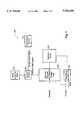
- FIG. 1is a block diagram of a memory system including an on-chip temperature sensor for regulating the refresh rate of a memory array;
- FIG. 2is a block diagram of another embodiment of a memory system including an on-chip temperature sensor for regulating the refresh rate of a DRAM cell configured to store multiple level logic states;
- FIG. 3is a block diagram illustrating the function of a memory cell and one embodiment of read/write circuitry for the memory system of FIG. 2;
- FIG. 4is a block diagram of an analog to digital converter capable of sensing more than two stored signal states
- the memory system 100includes a memory array 102 coupled to an address decoder and refresh control unit 104 and to a read/write control unit 106.
- a control circuit 108is further coupled to address decoder and refresh control unit 104.
- a temperature sensor 110 and ROM look-up table 112are finally shown coupled to control circuit 108.
- memory array 102includes a plurality of DRAM memory cells.
- Address decoder and refresh control unit 104is configured to perform address decoding functions and to refresh the cells of memory array 102.
- Read/write control unit 106accommodates read and write operations of data associated with memory array 102.
- Temperature sensor 110is provided to sense a temperature of a semiconductor die on which memory array 102 is fabricated, and to generate a temperature signal indicative of such temperature.
- Control circuit 108receives the temperature signal and generates a refresh rate signal which controls the refresh rate of the cells within memory array 102. That is, address decoder and refresh control unit 104 varies the refresh rate of the memory cells of memory array 102 depending upon the refresh rate signal from control circuit 108.
- ROM look-up table 112is provided to store a plurality of entries which each indicate a desired refresh rate for a particular temperature.
- Control circuit 108is configured to periodically access ROM look-up table 112 in accordance with the temperature signal received from temperature sensor 110, and to update the refresh rate signal according to the ROM look-up table entry which corresponds to the current temperature.
- the refresh rateis decreased as temperature increases.
- each cell of the memory arrayis configured to store more than two distinct logic states. Circuit portions that correspond to those of FIG. 1 are number identically for simplicity and clarity.
- memory system 200has a ground plane 202 surrounding the chip circuitry which shields the circuitry from electromagnetic noise.
- Memory system 200receives a chip enable signal, a read/write signal, and r address bit signals at an address decoder and refresh unit 104.
- address decoder and refresh unit 104asserts one of 2 r read word lines.
- Each of the read word linesis coupled to a row of memory cells.
- Each row of memory cellsis also coupled by a write word line to address controller 206.
- a read word lineis asserted, the corresponding row of memory cells may be read.
- a write word lineis asserted, the corresponding row of memory cells may be written.
- Memory system 200also has n bi-directional binary data lines (D 0 -D n-1 ) connected to a bi-directional gate 204.
- Bi-directional gate 204is coupled to receive the read/write signal and is further coupled to m data paths which carry multi-value logic signals (S 0 -S m-1 ).
- Each of the data pathscan be driven by either bi-directional gate 204 or one of a set of analog-to-digital (A/D) converters 216-1 through 216-m (referred to collectively as A/D converters 216).
- A/D converters 216analog-to-digital converters 216-1 through 216-m
- Each of the data pathsprovides input to one of a set of data line drivers 212-1 through 212-m (referred to collectively as data line drivers 212).
- Data line drivers 212each serve to convert the multi-value logic signal into a multi-level voltage signal which is coupled by a data write line to a corresponding column of memory cells. Each column of memory cells is also coupled by a data read line to one of a set of sense amplifiers 214-1 through 214-m, which in turn provides input to one of the A/D converters 216.
- A/D converters 216convert the amplified signals to m multi-value logic signals (S 0 -S m-1 ) which are coupled to bi-directional gate 204.
- Bi-directional gate 204converts the m multi-value logic signals (S 0 -S m-1 ) to n binary digital signals, and drives the n bits on data lines D 0 -D n-1 . In this manner, a multi-value logic state stored in each cell may be read.
- the cells being readare refreshed concurrent with the read operation (in addition to the normal refresh operations, as described below).
- data drivers 212convert the m multi-value logic signals (S 0 -S m-1 ) into m corresponding multi-level voltage signals and drive them on the data write lines which are coupled to cells 210. If at this time the word write line for word 0 is asserted, cells 210 store the m multi-level voltage signals. In this way, the content of cells 210 can be refreshed every time they are read.
- Bi-directional gate 204receives data from the bi-directional binary data lines D 0 -D n-1 and converts the data into m multi-value logic signals which are driven onto the m data paths.
- the A/D converters 216 for driving each of the m data pathsare disabled while the write/read control line indicates a write operation.
- Data line drivers 212convert the input m multi-value logic signals into m multi-level voltage signals and drives the data write lines coupled to the selected cells 210.
- bi-directional gate 204data line drivers 212, sense amplifiers 214, and A/D converters 216 collectively form a read/write control circuit.
- Other embodimentsmay employ different implementations of read/write circuitry.
- Address decoder and refresh unit 104further includes refresh circuitry to read and refresh the contents of each memory cell within a given time interval.
- the refresh cyclescan be implemented in many ways, one of which is to have them happening continuously while the chip is not enabled.
- bi-directional gate 204is disabled and the A/D converters 216 are enabled during refresh cycles.
- Address decoder and refresh unit 206may employ a counter which sequentially asserts each word line, causing a read operation similar to that described previously. In order to assure that each memory cell is refreshed, the chip must spend a specified fraction of a given time interval in the disabled mode.
- the refresh circuitrymay thus force the memory circuit in a disabled mode (i.e., prevent a write or read operation) to ensure that the cells 210 are refreshed appropriately.
- the memory system 200 of FIG. 2includes control circuit 108, temperature sensor 110, and ROM look-up table 112 which operate to adjust the refresh rate of address decoder and refresh control unit 104 in a manner as described previously with reference to FIG. 1.
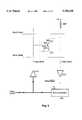
- FIG. 3illustrates a memory cell 210 which is exemplary of each of the cells of FIG. 2.
- Memory cell 210includes a storage transistor 302, a write transistor 304, and a read transistor 306.
- the gate of storage transistor 302is coupled via write transistor 304 to the data write line.
- Write transistor 304provides an electrically conductive path when the word write line is asserted, and an open circuit when the word line is de-asserted.
- an electric chargecan be stored on the gate by turning write transistor 304 on, passing a current through write transistor 304 to the gate of storage capacitor 302, and subsequently turning write transistor 304 off.
- the charge stored on the gatealters the conductivity of the channel of storage transistor 302.
- One terminal of storage transistor 302is connected to ground, and the other terminal is connected to read transistor 306.
- Read transistor 306provides an electrically conductive path when the word read line is asserted. The conductivity of storage transistor 302 can then be detected using the data read line.
- a pull-up resistance 309which may be implemented with a pull-up transistor, effects a voltage on the data read line which is indicative of the charge stored on the gate of storage transistor 302.
- Sense amplifier 214buffers and amplifies this voltage for A/D converter 216.
- A/D converter 216is enabled when the write/read signal indicates a read operation, and disabled when a write operation is indicated. When enabled, A/D converter 216 converts the amplified signal into a multi-value logic signal which is one of S 0 -S m-1
- Data line driver 212converts the multi-value logic signal into a multi-level voltage on the data write line.
- FIG. 4shows a block diagram of one embodiment of AID converter 216.
- A/D converter 216receives an input signal 402 and drives a digital output signal on L-1 output lines 404-408 (which form a data path to carry one of the multi-value logic signals S 0 -S m-1 ) when enabled by a write/read signal 410. During operation, asserting write/read signal 410 drives the output lines to a high impedance state.
- A/D converter 400is comprised of L-1 comparators 412, where L is the number of logic states which can be stored in a memory cell 308. Each comparator receives one of L-1 reference voltages which demarcate the voltage regions representative of each logic state.
- comparator 412-1compares input signal 402 to reference voltage V 1 , and (if enabled) asserts output line 404 when input signal 402 exceeds the reference voltage.
- the L-1 output linesaccordingly have L possible states, ranging from having no lines asserted to having L-1 lines asserted.
- bi-directional gate 204converts the input received at eight binary data lines D 0 -D 7 to four quaternary logic signals S 0 -S 3 .
- Each of the logic signalsis converted to a corresponding voltage on a data write line by a data line driver 212.
- the voltage at each data write lineresults in one of four charge quantities to be stored on the gate of storage transistor 302 being written.
- the charge stored on each storage transistor 302results in one of four possible channel conductivities which induces one of four possible voltages at the outputs of the sense amplifiers 214.
- the possible output voltagesmay be 0, V/3, 2V/3, and V, where V is the supply voltage.
- A/D converters 216each include three output lines and three reference voltages which maybe V/6, V/2, and 5V/6. Thus, if the output voltage of a particular cell 210 sensed by a sense amplifier 214 is 2V/3, two of the three output lines are asserted by A/D converter 216 (when enabled).
- each memory cell 210By adjusting the refresh rate of memory cells 210 in accordance with the refresh rate signal from control circuit 108, the proper charged state of each memory cell is maintained while accommodating adequate system performance. Since each cell of memory system 200 stores more than two discrete logical states, relatively high storage density may be achieved.
Landscapes
- Engineering & Computer Science (AREA)
- Computer Hardware Design (AREA)
- Microelectronics & Electronic Packaging (AREA)
- Dram (AREA)
Abstract
Description
Claims (18)
Priority Applications (3)
| Application Number | Priority Date | Filing Date | Title |
|---|---|---|---|
| US08/779,999US5784328A (en) | 1996-12-23 | 1996-12-23 | Memory system including an on-chip temperature sensor for regulating the refresh rate of a DRAM array |
| EP97122271AEP0851427A3 (en) | 1996-12-23 | 1997-12-17 | Memory system including an on-chip temperature sensor for regulating the refresh rate of a dram array |
| JP9370124AJPH10255467A (en) | 1996-12-23 | 1997-12-24 | Memory system including on-chip temperature sensor to adjust refresh speed of dram array |
Applications Claiming Priority (1)
| Application Number | Priority Date | Filing Date | Title |
|---|---|---|---|
| US08/779,999US5784328A (en) | 1996-12-23 | 1996-12-23 | Memory system including an on-chip temperature sensor for regulating the refresh rate of a DRAM array |
Publications (1)
| Publication Number | Publication Date |
|---|---|
| US5784328Atrue US5784328A (en) | 1998-07-21 |
Family
ID=25118256
Family Applications (1)
| Application Number | Title | Priority Date | Filing Date |
|---|---|---|---|
| US08/779,999Expired - LifetimeUS5784328A (en) | 1996-12-23 | 1996-12-23 | Memory system including an on-chip temperature sensor for regulating the refresh rate of a DRAM array |
Country Status (3)
| Country | Link |
|---|---|
| US (1) | US5784328A (en) |
| EP (1) | EP0851427A3 (en) |
| JP (1) | JPH10255467A (en) |
Cited By (91)
| Publication number | Priority date | Publication date | Assignee | Title |
|---|---|---|---|---|
| WO1999027429A1 (en)* | 1997-11-26 | 1999-06-03 | Intel Corporation | A method and apparatus to control core logic temperature |
| US5956289A (en)* | 1997-06-17 | 1999-09-21 | Micron Technology, Inc. | Clock signal from an adjustable oscillator for an integrated circuit |
| US6064627A (en)* | 1996-09-26 | 2000-05-16 | Mitsubishi Denki Kabushiki Kaisha | Synchronous semiconductor memory device |
| US6134167A (en)* | 1998-06-04 | 2000-10-17 | Compaq Computer Corporation | Reducing power consumption in computer memory |
| US6438057B1 (en)* | 2001-07-06 | 2002-08-20 | Infineon Technologies Ag | DRAM refresh timing adjustment device, system and method |
| US6453218B1 (en) | 1999-03-29 | 2002-09-17 | Intel Corporation | Integrated RAM thermal sensor |
| US6470238B1 (en) | 1997-11-26 | 2002-10-22 | Intel Corporation | Method and apparatus to control device temperature |
| US6496950B1 (en) | 1999-08-11 | 2002-12-17 | Lsi Logic Corporation | Testing content addressable static memories |
| US6550032B1 (en) | 1999-07-28 | 2003-04-15 | Lsi Logic Corporation | Detecting interport faults in multiport static memories |
| US6553452B2 (en)* | 1997-10-10 | 2003-04-22 | Rambus Inc. | Synchronous memory device having a temperature register |
| US6557072B2 (en)* | 2001-05-10 | 2003-04-29 | Palm, Inc. | Predictive temperature compensation for memory devices systems and method |
| US6560164B2 (en)* | 2001-01-23 | 2003-05-06 | Mitsubishi Denki Kabushiki Kaisha | Semiconductor integrated circuit device with internal clock generating circuit |
| US6564288B2 (en)* | 2000-11-30 | 2003-05-13 | Hewlett-Packard Company | Memory controller with temperature sensors |
| KR100386232B1 (en)* | 1998-09-01 | 2003-06-02 | 인텔 코오퍼레이션 | Control of memory access operations |
| US6577549B1 (en)* | 2001-12-03 | 2003-06-10 | Hewlett-Packard Company, L.P. | Write current compensation for temperature variations in memory arrays |
| US20030210598A1 (en)* | 2002-05-13 | 2003-11-13 | Alexander George William | Implementation of a temperature sensor to control internal chip voltages |
| US6667925B2 (en)* | 2001-10-29 | 2003-12-23 | Fujitsu Limited | Semiconductor device having temperature detecting function, testing method, and refresh control method of semiconductor storage device having temperature detecting function |
| US6714473B1 (en) | 2001-11-30 | 2004-03-30 | Cypress Semiconductor Corp. | Method and architecture for refreshing a 1T memory proportional to temperature |
| US20040066671A1 (en)* | 2001-08-31 | 2004-04-08 | Matrix Semiconductor, Inc. | Memory device and method for selectable sub-array activation |
| US20040088134A1 (en)* | 2002-10-31 | 2004-05-06 | Sun Microsystems, Inc | Sense amplifier thermal correction scheme |
| US6735546B2 (en)* | 2001-08-31 | 2004-05-11 | Matrix Semiconductor, Inc. | Memory device and method for temperature-based control over write and/or read operations |
| US20040100831A1 (en)* | 2002-11-27 | 2004-05-27 | Knall N. Johan | Integrated circuit and method for selecting a set of memory-cell-layer-dependent or temperature-dependent operating conditions |
| US6757854B1 (en) | 1999-09-16 | 2004-06-29 | Lsi Logic Corporation | Detecting faults in dual port FIFO memories |
| US6798706B2 (en)* | 2000-07-28 | 2004-09-28 | Infineon Technologies Ag | Integrated circuit with temperature sensor and method for heating the circuit |
| US6809914B2 (en)* | 2002-05-13 | 2004-10-26 | Infineon Technologies Ag | Use of DQ pins on a ram memory chip for a temperature sensing protocol |
| US20050018507A1 (en)* | 2003-07-17 | 2005-01-27 | Stephan Schroder | Circuit and method for controlling an access to an integrated memory |
| US6850856B1 (en)* | 2002-11-18 | 2005-02-01 | Sun Microsystems, Inc. | I/O receiver thermal correction scheme |
| US20050029663A1 (en)* | 2000-02-22 | 2005-02-10 | Micron Technology, Inc. | Polynorbornene foam insulation for integrated circuits |
| US20050078537A1 (en)* | 2003-09-30 | 2005-04-14 | Matrix Semiconductor, Inc. | Method and system for temperature compensation for memory cells with temperature-dependent behavior |
| US20050125597A1 (en)* | 2003-12-03 | 2005-06-09 | Simon Lovett | Compensated refresh oscillator |
| US20050141311A1 (en)* | 2003-12-29 | 2005-06-30 | Hynix Semiconductor, Inc. | Semiconductor memory device with optimum refresh cycle according to temperature variation |
| US20050162962A1 (en)* | 2003-04-23 | 2005-07-28 | Fujitsu Limited | Semiconductor memory device changing refresh interval depending on temperature |
| US20050190622A1 (en)* | 2004-02-27 | 2005-09-01 | Choi Joo S. | System and method for communicating information to a memory device using a reconfigured device pin |
| US20050249010A1 (en)* | 2004-05-06 | 2005-11-10 | Klein Dean A | Memory controller method and system compensating for memory cell data losses |
| US6965537B1 (en) | 2004-08-31 | 2005-11-15 | Micron Technology, Inc. | Memory system and method using ECC to achieve low power refresh |
| US20050289444A1 (en)* | 2004-06-25 | 2005-12-29 | Klein Dean A | Low power cost-effective ECC memory system and method |
| US20060002218A1 (en)* | 2004-06-30 | 2006-01-05 | Jain Sandeep K | Method and apparatus to implement a temperature control mechanism on a memory device |
| US20060006166A1 (en)* | 2004-07-06 | 2006-01-12 | Chen Howard H | On-chip power supply regulator and temperature control system |
| US20060010339A1 (en)* | 2004-06-24 | 2006-01-12 | Klein Dean A | Memory system and method having selective ECC during low power refresh |
| US20060013052A1 (en)* | 2004-07-15 | 2006-01-19 | Klein Dean A | Method and system for controlling refresh to avoid memory cell data losses |
| US20060046322A1 (en)* | 2004-08-31 | 2006-03-02 | Micron Technology, Inc. | Integrated circuit cooling and insulating device and method |
| US20060085616A1 (en)* | 2004-10-20 | 2006-04-20 | Zeighami Roy M | Method and system for dynamically adjusting DRAM refresh rate |
| US20060133125A1 (en)* | 2004-12-17 | 2006-06-22 | Matrix Semiconductor, Inc. | Apparatus and method for memory operations using address-dependent conditions |
| US20060185956A1 (en)* | 2005-02-21 | 2006-08-24 | Makoto Yasui | Rotation transmission device |
| US20060195289A1 (en)* | 2005-02-16 | 2006-08-31 | Samsung Electronics Co., Ltd. | Temperature sensor instruction signal generator and semiconductor memory device having the same |
| CN1297006C (en)* | 2001-05-31 | 2007-01-24 | 三星电子株式会社 | Clock generating circuit, integrated circuit storage devices and method for using said devices |
| US20070140315A1 (en)* | 2005-12-16 | 2007-06-21 | Micron Technology, Inc. | System and method for providing temperature data from a memory device having a temperature sensor |
| US7272063B1 (en)* | 2006-03-21 | 2007-09-18 | Infineon Technologies Ag | Memory with a temperature sensor, dynamic memory and memory with a clock unit and method of sensing a temperature of a memory |
| US7276788B1 (en) | 1999-08-25 | 2007-10-02 | Micron Technology, Inc. | Hydrophobic foamed insulators for high density circuits |
| US7277343B1 (en) | 2006-05-24 | 2007-10-02 | Sandisk 3D Llc | Memory device with improved temperature-sensor circuit |
| US20070242540A1 (en)* | 2006-04-03 | 2007-10-18 | Hynix Semiconductor Inc. | Semiconductor memory device with temperature sensing device and operation thereof |
| US20070262754A1 (en)* | 2006-05-11 | 2007-11-15 | Intel Corporation | Load circuit supply voltage control |
| US20070280023A1 (en)* | 2006-05-18 | 2007-12-06 | Thomas Happ | Phase change memory having temperature budget sensor |
| US20070280330A1 (en)* | 2006-05-31 | 2007-12-06 | Hynix Semiconductor Inc | On die thermal sensor of semiconductor memory device |
| US20070286259A1 (en)* | 2006-05-08 | 2007-12-13 | Samsung Electronics Co., Ltd. | Self-calibrating temperature sensors and methods thereof |
| US7335965B2 (en) | 1999-08-25 | 2008-02-26 | Micron Technology, Inc. | Packaging of electronic chips with air-bridge structures |
| US20080061760A1 (en)* | 2006-09-13 | 2008-03-13 | Hynix Semiconductor Inc. | Band gap reference circuit and temperature information output apparatus using the same |
| US20080106928A1 (en)* | 2006-09-20 | 2008-05-08 | Thomas Happ | Energy adjusted write pulses in phase-change memory cells |
| US20080117663A1 (en)* | 2006-11-22 | 2008-05-22 | Jan Boris Philipp | Resistive memory including refresh operation |
| KR100843226B1 (en) | 2007-01-08 | 2008-07-02 | 삼성전자주식회사 | On-chip temperature sensor and temperature detection method, refresh control method using the same |
| US20080158036A1 (en)* | 2007-01-03 | 2008-07-03 | Hynix Semiconductor Inc. | On die thermal sensor and method for generating thermal code of ODTS |
| US20090046531A1 (en)* | 2007-04-30 | 2009-02-19 | Samsung Electronics Co., Ltd. | Circuit and method for controlling refresh periods in semiconductor memory devices |
| US20090072882A1 (en)* | 2005-09-29 | 2009-03-19 | Chun-Seok Jeong | On die thermal sensor of semiconductor memory device and method thereof |
| US20090147607A1 (en)* | 2007-12-07 | 2009-06-11 | Nanya Technology Corporation | Random access memory and data refreshing method thereof |
| FR2927463A1 (en)* | 2008-02-12 | 2009-08-14 | Bull S A S Soc Par Actions Sim | Access control device i.e. memory controller, for double data rate type dynamic RAM in personal computer, has refresh control generator to maintain data in memory slots and selectively refresh memory locations indicated by register |
| US20090238020A1 (en)* | 2008-03-19 | 2009-09-24 | Peter Mayer | Integrated circuit including memory refreshed based on temperature |
| US20090323400A1 (en)* | 2008-06-27 | 2009-12-31 | Renesas Technology Corp. | Semiconductor device |
| US7745301B2 (en) | 2005-08-22 | 2010-06-29 | Terapede, Llc | Methods and apparatus for high-density chip connectivity |
| US20100220438A1 (en)* | 2007-12-27 | 2010-09-02 | Hisao Tsukazawa | Information processing apparatus and nonvolatile semiconductor storage device |
| CN101075478B (en)* | 2006-05-19 | 2010-10-13 | 富士通微电子株式会社 | Semiconductor memory and refresh cycle control method |
| US7831769B1 (en)* | 2004-11-02 | 2010-11-09 | Symantec Operating Corporation | System and method for performing online backup and restore of volume configuration information |
| US7894289B2 (en) | 2006-10-11 | 2011-02-22 | Micron Technology, Inc. | Memory system and method using partial ECC to achieve low power refresh and fast access to data |
| US7900120B2 (en) | 2006-10-18 | 2011-03-01 | Micron Technology, Inc. | Memory system and method using ECC with flag bit to identify modified data |
| US8684597B2 (en) | 2006-06-21 | 2014-04-01 | Intel Corporation | Thermal sensor having toggle control |
| US20140371945A1 (en)* | 2012-11-07 | 2014-12-18 | Canon Kabushiki Kaisha | Information processing apparatus, method for controlling the same and program |
| US8957511B2 (en) | 2005-08-22 | 2015-02-17 | Madhukar B. Vora | Apparatus and methods for high-density chip connectivity |
| US9786336B2 (en) | 2014-09-12 | 2017-10-10 | Samsung Electronics Co., Ltd. | Memory device capable of operation in wide temperature range and data processing system and method of operating the same |
| US9940046B2 (en) | 2015-11-27 | 2018-04-10 | Samsung Electronics Co., Ltd. | Semiconductor memory device with operation environment information storing circuit and command storing function |
| EP2772919B1 (en)* | 2010-12-10 | 2018-11-28 | Qualcomm Incorporated | DRAM refresh frequency determination |
| US10394618B2 (en)* | 2017-07-14 | 2019-08-27 | International Business Machines Corporation | Thermal and power memory actions |
| US10497420B1 (en)* | 2018-05-08 | 2019-12-03 | Micron Technology, Inc. | Memory with internal refresh rate control |
| CN110580925A (en)* | 2018-06-11 | 2019-12-17 | 南亚科技股份有限公司 | Storage device and method of operation thereof |
| US10831396B2 (en) | 2018-12-18 | 2020-11-10 | Micron Technology, Inc. | Data storage organization based on one or more stresses |
| US10910035B2 (en) | 2018-12-03 | 2021-02-02 | Samsung Electronics Co., Ltd. | Dynamic semiconductor memory device and memory system with temperature sensor |
| US10978136B2 (en)* | 2019-07-18 | 2021-04-13 | Apple Inc. | Dynamic refresh rate control |
| US10985162B2 (en) | 2018-12-14 | 2021-04-20 | John Bennett | System for accurate multiple level gain cells |
| US20210264970A1 (en)* | 2020-02-26 | 2021-08-26 | Taiwan Semiconductor Manufacturing Co., Ltd. | Method and system for refresh of memory devices |
| WO2021252830A1 (en)* | 2020-06-12 | 2021-12-16 | Micron Technology, Inc. | Motion sensor in memory |
| US11435811B2 (en)* | 2019-12-09 | 2022-09-06 | Micron Technology, Inc. | Memory device sensors |
| US12061125B2 (en) | 2020-04-16 | 2024-08-13 | Macronix International Co., Ltd. | Temperature sensor and memory device having same |
| CN119541576A (en)* | 2023-08-29 | 2025-02-28 | 长江存储科技有限责任公司 | Memory and operation method thereof, memory system and electronic device |
Families Citing this family (28)
| Publication number | Priority date | Publication date | Assignee | Title |
|---|---|---|---|---|
| US6021076A (en) | 1998-07-16 | 2000-02-01 | Rambus Inc | Apparatus and method for thermal regulation in memory subsystems |
| DE19983470B4 (en)* | 1998-08-18 | 2011-08-18 | Intel Corporation, Calif. | Method and device for controlling the temperature of a component |
| JP4700223B2 (en)* | 2001-05-18 | 2011-06-15 | 株式会社バッファロー | DRAM device and DRAM device refresh method |
| DE10163306A1 (en)* | 2001-12-21 | 2003-04-03 | Infineon Technologies Ag | Dynamic memory (DRAM) with programmable brush-up frequency |
| DE10329369B4 (en)* | 2003-06-30 | 2010-01-28 | Qimonda Ag | Circuit and method for refreshing memory cells of a dynamic memory |
| DE10329370B3 (en) | 2003-06-30 | 2005-01-27 | Infineon Technologies Ag | Circuit for refreshing memory cells in a dynamic memory has a refresh control circuit, a memory circuit, a setting circuit and a reset circuit |
| US8122187B2 (en) | 2004-07-02 | 2012-02-21 | Qualcomm Incorporated | Refreshing dynamic volatile memory |
| US7206244B2 (en)* | 2004-12-01 | 2007-04-17 | Freescale Semiconductor, Inc. | Temperature based DRAM refresh |
| US7230876B2 (en)* | 2005-02-14 | 2007-06-12 | Qualcomm Incorporated | Register read for volatile memory |
| US7620783B2 (en) | 2005-02-14 | 2009-11-17 | Qualcomm Incorporated | Method and apparatus for obtaining memory status information cross-reference to related applications |
| US7640392B2 (en) | 2005-06-23 | 2009-12-29 | Qualcomm Incorporated | Non-DRAM indicator and method of accessing data not stored in DRAM array |
| KR100766379B1 (en) | 2006-08-11 | 2007-10-12 | 주식회사 하이닉스반도체 | Temperature Sensing Circuit in Semiconductor Memory Device |
| US9262326B2 (en) | 2006-08-14 | 2016-02-16 | Qualcomm Incorporated | Method and apparatus to enable the cooperative signaling of a shared bus interrupt in a multi-rank memory subsystem |
| KR100738969B1 (en) | 2006-08-16 | 2007-07-12 | 주식회사 하이닉스반도체 | Apparatus and method for controlling on-die termination of semiconductor memory |
| KR100807594B1 (en) | 2006-09-28 | 2008-02-28 | 주식회사 하이닉스반도체 | Temperature information output device and semiconductor device having same |
| KR100808054B1 (en) | 2006-10-31 | 2008-02-28 | 주식회사 하이닉스반도체 | Low power temperature information output device |
| KR100806608B1 (en) | 2006-11-02 | 2008-02-25 | 주식회사 하이닉스반도체 | Temperature information output device of semiconductor memory device with analog-to-digital converter, analog-to-digital converting method and analog-to-digital converter |
| KR100810061B1 (en) | 2006-11-02 | 2008-03-05 | 주식회사 하이닉스반도체 | Temperature information output device and internal temperature measuring method of semiconductor memory device |
| KR100806609B1 (en) | 2006-11-02 | 2008-02-25 | 주식회사 하이닉스반도체 | Temperature information output device of semiconductor memory device |
| KR100909251B1 (en) | 2007-01-31 | 2009-07-23 | 주식회사 하이닉스반도체 | Analog-to-digital converter and temperature information output device including the same |
| KR100875666B1 (en) | 2007-03-31 | 2008-12-24 | 주식회사 하이닉스반도체 | Semiconductor memory device |
| DE202008011848U1 (en)* | 2008-09-04 | 2010-02-11 | Sick Ag | Optoelectronic sensor |
| KR100980417B1 (en) | 2008-12-09 | 2010-09-07 | 주식회사 하이닉스반도체 | Data driver |
| US7929368B2 (en) | 2008-12-30 | 2011-04-19 | Micron Technology, Inc. | Variable memory refresh devices and methods |
| JP4691183B2 (en)* | 2009-08-31 | 2011-06-01 | 株式会社東芝 | Multilevel semiconductor memory device and information processing device |
| JP4996768B2 (en)* | 2011-11-21 | 2012-08-08 | 株式会社東芝 | Storage device and SSD |
| JP5498529B2 (en)* | 2012-05-11 | 2014-05-21 | 株式会社東芝 | Storage device and information processing apparatus |
| US11550687B2 (en) | 2019-12-09 | 2023-01-10 | Micron Technology, Inc. | Using memory device sensors |
Citations (23)
| Publication number | Priority date | Publication date | Assignee | Title |
|---|---|---|---|---|
| US4057788A (en)* | 1974-10-21 | 1977-11-08 | Raytheon Company | Semiconductor memory structures |
| US4633438A (en)* | 1983-12-19 | 1986-12-30 | Hitachi, Ltd. | Stacked semiconductor memory |
| US4661929A (en)* | 1983-12-23 | 1987-04-28 | Hitachi, Ltd. | Semiconductor memory having multiple level storage structure |
| US4715014A (en)* | 1985-10-29 | 1987-12-22 | Texas Instruments Incorporated | Modified three transistor EEPROM cell |
| US4910709A (en)* | 1988-08-10 | 1990-03-20 | International Business Machines Corporation | Complementary metal-oxide-semiconductor transistor and one-capacitor dynamic-random-access memory cell |
| US4935896A (en)* | 1987-11-24 | 1990-06-19 | Mitsubishi Denki Kabushiki Kaisha | Semiconductor memory device having three-transistor type memory cells structure without additional gates |
| US5021999A (en)* | 1987-12-17 | 1991-06-04 | Mitsubishi Denki Kabushiki Kaisha | Non-volatile semiconductor memory device with facility of storing tri-level data |
| US5119330A (en)* | 1989-03-31 | 1992-06-02 | Oki Electric Industry Co, Ltd. | Nonvolatile memory system for multiple value storing |
| US5159570A (en)* | 1987-12-22 | 1992-10-27 | Texas Instruments Incorporated | Four memory state EEPROM |
| US5172338A (en)* | 1989-04-13 | 1992-12-15 | Sundisk Corporation | Multi-state EEprom read and write circuits and techniques |
| US5276843A (en)* | 1991-04-12 | 1994-01-04 | Micron Technology, Inc. | Dynamic RAM array for emulating a static RAM array |
| US5278796A (en)* | 1991-04-12 | 1994-01-11 | Micron Technology, Inc. | Temperature-dependent DRAM refresh circuit |
| US5282162A (en)* | 1990-05-24 | 1994-01-25 | Kabushiki Kaisha Toshiba | Semiconductor memory device having capacitor of thin film transistor structure |
| US5283761A (en)* | 1992-07-22 | 1994-02-01 | Mosaid Technologies Incorporated | Method of multi-level storage in DRAM |
| US5351210A (en)* | 1990-11-28 | 1994-09-27 | Kabushiki Kaisha Toshiba | Serially accessible semiconductor memory with multiple level storage cells |
| US5357464A (en)* | 1992-03-02 | 1994-10-18 | Hitachi, Ltd. | Semiconductor memory having writing and reading transistors, method of fabrication thereof, and method of use thereof |
| US5394362A (en)* | 1991-02-08 | 1995-02-28 | Banks; Gerald J. | Electrically alterable non-voltatile memory with N-bits per memory cell |
| US5459686A (en)* | 1993-10-15 | 1995-10-17 | Solidas Corporation | Multiple level random access memory |
| US5521865A (en)* | 1994-03-15 | 1996-05-28 | Kabushiki Kaisha Toshiba | Non-volatile semiconductor memory device for storing multi-value data |
| US5532955A (en)* | 1994-12-30 | 1996-07-02 | Mosaid Technologies Incorporated | Method of multilevel dram sense and restore |
| US5596534A (en)* | 1995-06-27 | 1997-01-21 | Micron Technology, Inc. | Circuit including DRAM and voltage regulator, and method of increasing speed of operation of a DRAM |
| US5600591A (en)* | 1992-04-24 | 1997-02-04 | Mitsubishi Denki Kabushiki Kaisha | Dynamic random access memory and manufacturing method thereof |
| US5652729A (en)* | 1995-02-08 | 1997-07-29 | Matsushita Electric Industrial Co., Ltd. | Semiconductor integrated circuit apparatus and method of adjusting refresh timer cycle |
Family Cites Families (2)
| Publication number | Priority date | Publication date | Assignee | Title |
|---|---|---|---|---|
| KR0129197B1 (en)* | 1994-04-21 | 1998-10-01 | 문정환 | Refresh control circuit of memory cell array |
| JPH08180688A (en)* | 1994-12-26 | 1996-07-12 | Nec Corp | Semiconductor memory |
- 1996
- 1996-12-23USUS08/779,999patent/US5784328A/ennot_activeExpired - Lifetime
- 1997
- 1997-12-17EPEP97122271Apatent/EP0851427A3/ennot_activeWithdrawn
- 1997-12-24JPJP9370124Apatent/JPH10255467A/enactivePending
Patent Citations (24)
| Publication number | Priority date | Publication date | Assignee | Title |
|---|---|---|---|---|
| US4057788A (en)* | 1974-10-21 | 1977-11-08 | Raytheon Company | Semiconductor memory structures |
| US4633438A (en)* | 1983-12-19 | 1986-12-30 | Hitachi, Ltd. | Stacked semiconductor memory |
| US4661929A (en)* | 1983-12-23 | 1987-04-28 | Hitachi, Ltd. | Semiconductor memory having multiple level storage structure |
| US4715014A (en)* | 1985-10-29 | 1987-12-22 | Texas Instruments Incorporated | Modified three transistor EEPROM cell |
| US4935896A (en)* | 1987-11-24 | 1990-06-19 | Mitsubishi Denki Kabushiki Kaisha | Semiconductor memory device having three-transistor type memory cells structure without additional gates |
| US5021999A (en)* | 1987-12-17 | 1991-06-04 | Mitsubishi Denki Kabushiki Kaisha | Non-volatile semiconductor memory device with facility of storing tri-level data |
| US5159570A (en)* | 1987-12-22 | 1992-10-27 | Texas Instruments Incorporated | Four memory state EEPROM |
| US4910709A (en)* | 1988-08-10 | 1990-03-20 | International Business Machines Corporation | Complementary metal-oxide-semiconductor transistor and one-capacitor dynamic-random-access memory cell |
| US5119330A (en)* | 1989-03-31 | 1992-06-02 | Oki Electric Industry Co, Ltd. | Nonvolatile memory system for multiple value storing |
| US5172338A (en)* | 1989-04-13 | 1992-12-15 | Sundisk Corporation | Multi-state EEprom read and write circuits and techniques |
| US5172338B1 (en)* | 1989-04-13 | 1997-07-08 | Sandisk Corp | Multi-state eeprom read and write circuits and techniques |
| US5282162A (en)* | 1990-05-24 | 1994-01-25 | Kabushiki Kaisha Toshiba | Semiconductor memory device having capacitor of thin film transistor structure |
| US5351210A (en)* | 1990-11-28 | 1994-09-27 | Kabushiki Kaisha Toshiba | Serially accessible semiconductor memory with multiple level storage cells |
| US5394362A (en)* | 1991-02-08 | 1995-02-28 | Banks; Gerald J. | Electrically alterable non-voltatile memory with N-bits per memory cell |
| US5278796A (en)* | 1991-04-12 | 1994-01-11 | Micron Technology, Inc. | Temperature-dependent DRAM refresh circuit |
| US5276843A (en)* | 1991-04-12 | 1994-01-04 | Micron Technology, Inc. | Dynamic RAM array for emulating a static RAM array |
| US5357464A (en)* | 1992-03-02 | 1994-10-18 | Hitachi, Ltd. | Semiconductor memory having writing and reading transistors, method of fabrication thereof, and method of use thereof |
| US5600591A (en)* | 1992-04-24 | 1997-02-04 | Mitsubishi Denki Kabushiki Kaisha | Dynamic random access memory and manufacturing method thereof |
| US5283761A (en)* | 1992-07-22 | 1994-02-01 | Mosaid Technologies Incorporated | Method of multi-level storage in DRAM |
| US5459686A (en)* | 1993-10-15 | 1995-10-17 | Solidas Corporation | Multiple level random access memory |
| US5521865A (en)* | 1994-03-15 | 1996-05-28 | Kabushiki Kaisha Toshiba | Non-volatile semiconductor memory device for storing multi-value data |
| US5532955A (en)* | 1994-12-30 | 1996-07-02 | Mosaid Technologies Incorporated | Method of multilevel dram sense and restore |
| US5652729A (en)* | 1995-02-08 | 1997-07-29 | Matsushita Electric Industrial Co., Ltd. | Semiconductor integrated circuit apparatus and method of adjusting refresh timer cycle |
| US5596534A (en)* | 1995-06-27 | 1997-01-21 | Micron Technology, Inc. | Circuit including DRAM and voltage regulator, and method of increasing speed of operation of a DRAM |
Non-Patent Citations (2)
| Title |
|---|
| Abbott, et al., "A 4K MOS Dynamic Random-Access Memory," IEEE Journal of Solid-State Circuits, vol. SC-8, No. 5, Oct. 1973, pp. 292-298. |
| Abbott, et al., A 4K MOS Dynamic Random Access Memory, IEEE Journal of Solid State Circuits, vol. SC 8, No. 5, Oct. 1973, pp. 292 298.* |
Cited By (208)
| Publication number | Priority date | Publication date | Assignee | Title |
|---|---|---|---|---|
| US6064627A (en)* | 1996-09-26 | 2000-05-16 | Mitsubishi Denki Kabushiki Kaisha | Synchronous semiconductor memory device |
| US5956289A (en)* | 1997-06-17 | 1999-09-21 | Micron Technology, Inc. | Clock signal from an adjustable oscillator for an integrated circuit |
| US6160755A (en)* | 1997-06-17 | 2000-12-12 | Micron Technology, Inc. | Clock signal from an adjustable oscillator for an integrated circuit |
| US6553452B2 (en)* | 1997-10-10 | 2003-04-22 | Rambus Inc. | Synchronous memory device having a temperature register |
| US7337294B2 (en) | 1997-10-10 | 2008-02-26 | Rambus Inc. | Method and apparatus for adjusting the performance of a synchronous memory system |
| US20080162759A1 (en)* | 1997-10-10 | 2008-07-03 | Rambus Inc. | Method and apparatus for adjusting the performance of a synchronous memory system |
| US8296540B2 (en) | 1997-10-10 | 2012-10-23 | Rambus Inc. | Method and apparatus for adjusting the performance of a synchronous memory system |
| US20070083700A1 (en)* | 1997-10-10 | 2007-04-12 | Rambus Inc. | Method and apparatus for adjusting the performance of a synchronous memory system |
| WO1999027429A1 (en)* | 1997-11-26 | 1999-06-03 | Intel Corporation | A method and apparatus to control core logic temperature |
| US5953685A (en)* | 1997-11-26 | 1999-09-14 | Intel Corporation | Method and apparatus to control core logic temperature |
| US6470238B1 (en) | 1997-11-26 | 2002-10-22 | Intel Corporation | Method and apparatus to control device temperature |
| US6173217B1 (en) | 1997-11-26 | 2001-01-09 | Intel Corporation | Method and apparatus to control core logic temperature |
| US6134167A (en)* | 1998-06-04 | 2000-10-17 | Compaq Computer Corporation | Reducing power consumption in computer memory |
| KR100386232B1 (en)* | 1998-09-01 | 2003-06-02 | 인텔 코오퍼레이션 | Control of memory access operations |
| US6453218B1 (en) | 1999-03-29 | 2002-09-17 | Intel Corporation | Integrated RAM thermal sensor |
| US6550032B1 (en) | 1999-07-28 | 2003-04-15 | Lsi Logic Corporation | Detecting interport faults in multiport static memories |
| US6496950B1 (en) | 1999-08-11 | 2002-12-17 | Lsi Logic Corporation | Testing content addressable static memories |
| US7276788B1 (en) | 1999-08-25 | 2007-10-02 | Micron Technology, Inc. | Hydrophobic foamed insulators for high density circuits |
| US7387912B2 (en) | 1999-08-25 | 2008-06-17 | Micron Technology, Inc. | Packaging of electronic chips with air-bridge structures |
| US7335965B2 (en) | 1999-08-25 | 2008-02-26 | Micron Technology, Inc. | Packaging of electronic chips with air-bridge structures |
| US6757854B1 (en) | 1999-09-16 | 2004-06-29 | Lsi Logic Corporation | Detecting faults in dual port FIFO memories |
| US20050029663A1 (en)* | 2000-02-22 | 2005-02-10 | Micron Technology, Inc. | Polynorbornene foam insulation for integrated circuits |
| US6798706B2 (en)* | 2000-07-28 | 2004-09-28 | Infineon Technologies Ag | Integrated circuit with temperature sensor and method for heating the circuit |
| KR100827863B1 (en) | 2000-07-28 | 2008-05-07 | 인피네온 테크놀로지스 아게 | How to maintain temperature |
| US6564288B2 (en)* | 2000-11-30 | 2003-05-13 | Hewlett-Packard Company | Memory controller with temperature sensors |
| US6560164B2 (en)* | 2001-01-23 | 2003-05-06 | Mitsubishi Denki Kabushiki Kaisha | Semiconductor integrated circuit device with internal clock generating circuit |
| US6557072B2 (en)* | 2001-05-10 | 2003-04-29 | Palm, Inc. | Predictive temperature compensation for memory devices systems and method |
| CN1297006C (en)* | 2001-05-31 | 2007-01-24 | 三星电子株式会社 | Clock generating circuit, integrated circuit storage devices and method for using said devices |
| KR20030011257A (en)* | 2001-07-06 | 2003-02-07 | 인피네온 테크놀로지스 아게 | Dram refresh timing adjustment device, system, and method |
| DE10228719B4 (en)* | 2001-07-06 | 2014-02-06 | Qimonda Ag | Apparatus and system for setting the DRAM refresh timing |
| US6438057B1 (en)* | 2001-07-06 | 2002-08-20 | Infineon Technologies Ag | DRAM refresh timing adjustment device, system and method |
| US6724665B2 (en) | 2001-08-31 | 2004-04-20 | Matrix Semiconductor, Inc. | Memory device and method for selectable sub-array activation |
| US6735546B2 (en)* | 2001-08-31 | 2004-05-11 | Matrix Semiconductor, Inc. | Memory device and method for temperature-based control over write and/or read operations |
| US6894936B2 (en) | 2001-08-31 | 2005-05-17 | Matrix Semiconductor, Inc. | Memory device and method for selectable sub-array activation |
| US20040066671A1 (en)* | 2001-08-31 | 2004-04-08 | Matrix Semiconductor, Inc. | Memory device and method for selectable sub-array activation |
| US6667925B2 (en)* | 2001-10-29 | 2003-12-23 | Fujitsu Limited | Semiconductor device having temperature detecting function, testing method, and refresh control method of semiconductor storage device having temperature detecting function |
| US6714473B1 (en) | 2001-11-30 | 2004-03-30 | Cypress Semiconductor Corp. | Method and architecture for refreshing a 1T memory proportional to temperature |
| US6577549B1 (en)* | 2001-12-03 | 2003-06-10 | Hewlett-Packard Company, L.P. | Write current compensation for temperature variations in memory arrays |
| US20030210598A1 (en)* | 2002-05-13 | 2003-11-13 | Alexander George William | Implementation of a temperature sensor to control internal chip voltages |
| US6809978B2 (en)* | 2002-05-13 | 2004-10-26 | Infineon Technologies Ag | Implementation of a temperature sensor to control internal chip voltages |
| US6809914B2 (en)* | 2002-05-13 | 2004-10-26 | Infineon Technologies Ag | Use of DQ pins on a ram memory chip for a temperature sensing protocol |
| US20040088134A1 (en)* | 2002-10-31 | 2004-05-06 | Sun Microsystems, Inc | Sense amplifier thermal correction scheme |
| US6879929B2 (en)* | 2002-10-31 | 2005-04-12 | Sun Microsystems | Sense amplifier thermal correction scheme |
| US6850856B1 (en)* | 2002-11-18 | 2005-02-01 | Sun Microsystems, Inc. | I/O receiver thermal correction scheme |
| US6954394B2 (en) | 2002-11-27 | 2005-10-11 | Matrix Semiconductor, Inc. | Integrated circuit and method for selecting a set of memory-cell-layer-dependent or temperature-dependent operating conditions |
| US20040100831A1 (en)* | 2002-11-27 | 2004-05-27 | Knall N. Johan | Integrated circuit and method for selecting a set of memory-cell-layer-dependent or temperature-dependent operating conditions |
| US8472275B2 (en) | 2003-04-23 | 2013-06-25 | Fujitsu Semiconductor Limited | Semiconductor memory device changing refresh interval depending on temperature |
| US20050162962A1 (en)* | 2003-04-23 | 2005-07-28 | Fujitsu Limited | Semiconductor memory device changing refresh interval depending on temperature |
| US20090040856A1 (en)* | 2003-04-23 | 2009-02-12 | Fujitsu Limited | Semiconductor memory device changing refresh interval depending on temperature |
| US7196956B2 (en)* | 2003-04-23 | 2007-03-27 | Fujitsu Limited | Semiconductor memory device changing refresh interval depending on temperature |
| US8867293B2 (en) | 2003-04-23 | 2014-10-21 | Fujitsu Semiconductor Limited | Semiconductor memory device changing refresh interval depending on temperature |
| US20050018507A1 (en)* | 2003-07-17 | 2005-01-27 | Stephan Schroder | Circuit and method for controlling an access to an integrated memory |
| US7085185B2 (en)* | 2003-07-17 | 2006-08-01 | Infineon Technologies Ag | Circuit and method for controlling an access to an integrated memory |
| US7057958B2 (en) | 2003-09-30 | 2006-06-06 | Sandisk Corporation | Method and system for temperature compensation for memory cells with temperature-dependent behavior |
| US20050078537A1 (en)* | 2003-09-30 | 2005-04-14 | Matrix Semiconductor, Inc. | Method and system for temperature compensation for memory cells with temperature-dependent behavior |
| US20050125597A1 (en)* | 2003-12-03 | 2005-06-09 | Simon Lovett | Compensated refresh oscillator |
| US7272065B2 (en)* | 2003-12-03 | 2007-09-18 | Simon Lovett | Compensated refresh oscillator |
| US20050141311A1 (en)* | 2003-12-29 | 2005-06-30 | Hynix Semiconductor, Inc. | Semiconductor memory device with optimum refresh cycle according to temperature variation |
| US8520450B2 (en) | 2003-12-29 | 2013-08-27 | Hynix Semiconductor Inc. | Semiconductor memory device with optimum refresh cycle according to temperature variation |
| US7990776B2 (en)* | 2003-12-29 | 2011-08-02 | Hynix Semiconductor Inc. | Semiconductor memory device with optimum refresh cycle according to temperature variation |
| US7158422B2 (en) | 2004-02-27 | 2007-01-02 | Micron Technology, Inc. | System and method for communicating information to a memory device using a reconfigured device pin |
| US20060120131A1 (en)* | 2004-02-27 | 2006-06-08 | Choi Joo S | System and method for communicating information to a memory device using a reconfigured device pin |
| US20050190622A1 (en)* | 2004-02-27 | 2005-09-01 | Choi Joo S. | System and method for communicating information to a memory device using a reconfigured device pin |
| US7315476B2 (en) | 2004-02-27 | 2008-01-01 | Micron Technology, Inc. | System and method for communicating information to a memory device using a reconfigured device pin |
| US7428687B2 (en) | 2004-05-06 | 2008-09-23 | Micron Technology, Inc. | Memory controller method and system compensating for memory cell data losses |
| US20060069856A1 (en)* | 2004-05-06 | 2006-03-30 | Klein Dean A | Memory controller method and system compensating for memory cell data losses |
| US20060056259A1 (en)* | 2004-05-06 | 2006-03-16 | Klein Dean A | Memory controller method and system compensating for memory cell data losses |
| US20060056260A1 (en)* | 2004-05-06 | 2006-03-16 | Klein Dean A | Memory controller method and system compensating for memory cell data losses |
| US7836374B2 (en)* | 2004-05-06 | 2010-11-16 | Micron Technology, Inc. | Memory controller method and system compensating for memory cell data losses |
| US7447974B2 (en) | 2004-05-06 | 2008-11-04 | Micron Technology, Inc. | Memory controller method and system compensating for memory cell data losses |
| US7099221B2 (en) | 2004-05-06 | 2006-08-29 | Micron Technology, Inc. | Memory controller method and system compensating for memory cell data losses |
| US8689077B2 (en) | 2004-05-06 | 2014-04-01 | Micron Technology, Inc. | Memory controller method and system compensating for memory cell data losses |
| US20050249010A1 (en)* | 2004-05-06 | 2005-11-10 | Klein Dean A | Memory controller method and system compensating for memory cell data losses |
| US7447973B2 (en) | 2004-05-06 | 2008-11-04 | Micron Technology, Inc. | Memory controller method and system compensating for memory cell data losses |
| US9064600B2 (en) | 2004-05-06 | 2015-06-23 | Micron Technology, Inc. | Memory controller method and system compensating for memory cell data losses |
| US20060010339A1 (en)* | 2004-06-24 | 2006-01-12 | Klein Dean A | Memory system and method having selective ECC during low power refresh |
| US7461320B2 (en) | 2004-06-24 | 2008-12-02 | Micron Technology, Inc. | Memory system and method having selective ECC during low power refresh |
| US20060206769A1 (en)* | 2004-06-24 | 2006-09-14 | Klein Dean A | Memory system and method having selective ECC during low power refresh |
| US7526713B2 (en) | 2004-06-25 | 2009-04-28 | Micron Technology, Inc. | Low power cost-effective ECC memory system and method |
| US20050289444A1 (en)* | 2004-06-25 | 2005-12-29 | Klein Dean A | Low power cost-effective ECC memory system and method |
| US7340668B2 (en) | 2004-06-25 | 2008-03-04 | Micron Technology, Inc. | Low power cost-effective ECC memory system and method |
| US20060002218A1 (en)* | 2004-06-30 | 2006-01-05 | Jain Sandeep K | Method and apparatus to implement a temperature control mechanism on a memory device |
| US7145823B2 (en)* | 2004-06-30 | 2006-12-05 | Intel Corporation | Method and apparatus to implement a temperature control mechanism on a memory device |
| US7214910B2 (en)* | 2004-07-06 | 2007-05-08 | International Business Machines Corporation | On-chip power supply regulator and temperature control system |
| US20060006166A1 (en)* | 2004-07-06 | 2006-01-12 | Chen Howard H | On-chip power supply regulator and temperature control system |
| US7272066B2 (en) | 2004-07-15 | 2007-09-18 | Micron Technology, Inc. | Method and system for controlling refresh to avoid memory cell data losses |
| US7558142B2 (en) | 2004-07-15 | 2009-07-07 | Micron Technology, Inc. | Method and system for controlling refresh to avoid memory cell data losses |
| US8279683B2 (en) | 2004-07-15 | 2012-10-02 | Micron Technology, Inc. | Digit line comparison circuits |
| US8446783B2 (en) | 2004-07-15 | 2013-05-21 | Micron Technology, Inc. | Digit line comparison circuits |
| US7116602B2 (en) | 2004-07-15 | 2006-10-03 | Micron Technology, Inc. | Method and system for controlling refresh to avoid memory cell data losses |
| US20060013052A1 (en)* | 2004-07-15 | 2006-01-19 | Klein Dean A | Method and system for controlling refresh to avoid memory cell data losses |
| US20060158950A1 (en)* | 2004-07-15 | 2006-07-20 | Klein Dean A | Method and system for controlling refresh to avoid memory cell data losses |
| US20080002503A1 (en)* | 2004-07-15 | 2008-01-03 | Klein Dean A | Method and system for controlling refresh to avoid memory cell data losses |
| US7898892B2 (en) | 2004-07-15 | 2011-03-01 | Micron Technology, Inc. | Method and system for controlling refresh to avoid memory cell data losses |
| US7277345B2 (en) | 2004-07-15 | 2007-10-02 | Micron Technology, Inc. | Method and system for controlling refresh to avoid memory cell data losses |
| US20060152989A1 (en)* | 2004-07-15 | 2006-07-13 | Klein Dean A | Method and system for controlling refresh to avoid memory cell data losses |
| US7280386B2 (en) | 2004-07-15 | 2007-10-09 | Micron Technology, Inc. | Method and system for controlling refresh to avoid memory cell data losses |
| US7623392B2 (en) | 2004-07-15 | 2009-11-24 | Micron Technology, Inc. | Method and system for controlling refresh to avoid memory cell data losses |
| US7300821B2 (en) | 2004-08-31 | 2007-11-27 | Micron Technology, Inc. | Integrated circuit cooling and insulating device and method |
| US20080057629A1 (en)* | 2004-08-31 | 2008-03-06 | Micron Technology, Inc. | Integrated circuit cooling and insulating device and method |
| US20080048314A1 (en)* | 2004-08-31 | 2008-02-28 | Micron Technology, Inc. | Integrated circuit cooling and insulating device and method |
| US7184352B2 (en) | 2004-08-31 | 2007-02-27 | Micron Technology, Inc. | Memory system and method using ECC to achieve low power refresh |
| US20060044913A1 (en)* | 2004-08-31 | 2006-03-02 | Klein Dean A | Memory system and method using ECC to achieve low power refresh |
| US20060046322A1 (en)* | 2004-08-31 | 2006-03-02 | Micron Technology, Inc. | Integrated circuit cooling and insulating device and method |
| US7492042B2 (en) | 2004-08-31 | 2009-02-17 | Micron Technology, Inc. | Integrated circuit cooling and insulating device and method |
| US7485497B2 (en) | 2004-08-31 | 2009-02-03 | Micron Technology, Inc. | Integrated circuit cooling and insulating device and method |
| US6965537B1 (en) | 2004-08-31 | 2005-11-15 | Micron Technology, Inc. | Memory system and method using ECC to achieve low power refresh |
| US20060085616A1 (en)* | 2004-10-20 | 2006-04-20 | Zeighami Roy M | Method and system for dynamically adjusting DRAM refresh rate |
| US7305518B2 (en) | 2004-10-20 | 2007-12-04 | Hewlett-Packard Development Company, L.P. | Method and system for dynamically adjusting DRAM refresh rate |
| US7831769B1 (en)* | 2004-11-02 | 2010-11-09 | Symantec Operating Corporation | System and method for performing online backup and restore of volume configuration information |
| US7218570B2 (en) | 2004-12-17 | 2007-05-15 | Sandisk 3D Llc | Apparatus and method for memory operations using address-dependent conditions |
| US20060133125A1 (en)* | 2004-12-17 | 2006-06-22 | Matrix Semiconductor, Inc. | Apparatus and method for memory operations using address-dependent conditions |
| US20060195289A1 (en)* | 2005-02-16 | 2006-08-31 | Samsung Electronics Co., Ltd. | Temperature sensor instruction signal generator and semiconductor memory device having the same |
| US7499359B2 (en) | 2005-02-16 | 2009-03-03 | Samsung Electronics Co., Ltd. | Temperature sensor instruction signal generator and semiconductor memory device having the same |
| US20060185956A1 (en)* | 2005-02-21 | 2006-08-24 | Makoto Yasui | Rotation transmission device |
| US8957511B2 (en) | 2005-08-22 | 2015-02-17 | Madhukar B. Vora | Apparatus and methods for high-density chip connectivity |
| US7745301B2 (en) | 2005-08-22 | 2010-06-29 | Terapede, Llc | Methods and apparatus for high-density chip connectivity |
| US7953569B2 (en) | 2005-09-29 | 2011-05-31 | Hynix Semiconductor Inc. | On die thermal sensor of semiconductor memory device and method thereof |
| US20090072882A1 (en)* | 2005-09-29 | 2009-03-19 | Chun-Seok Jeong | On die thermal sensor of semiconductor memory device and method thereof |
| US20090052268A1 (en)* | 2005-12-16 | 2009-02-26 | Micron Technology, Inc. | System and method for providing temperature data from a memory device having a temperature sensor |
| US8186878B2 (en) | 2005-12-16 | 2012-05-29 | Round Rock Research, Llc | System and method for providing temperature data from a memory device having a temperature sensor |
| US7677796B2 (en) | 2005-12-16 | 2010-03-16 | Micron Technology, Inc. | System and method for providing temperature data from a memory device having a temperature sensor |
| US20070140315A1 (en)* | 2005-12-16 | 2007-06-21 | Micron Technology, Inc. | System and method for providing temperature data from a memory device having a temperature sensor |
| US7441949B2 (en) | 2005-12-16 | 2008-10-28 | Micron Technology, Inc. | System and method for providing temperature data from a memory device having a temperature sensor |
| US20100142287A1 (en)* | 2005-12-16 | 2010-06-10 | Micron Technology, Inc. | System and method for providing temperature data from a memory device having a temperature sensor |
| US20070223299A1 (en)* | 2006-03-21 | 2007-09-27 | Egerer Jens C | Memory with a temperature sensor, dynamic memory and memory with a clock unit and method of sensing a temperature of a memory |
| US7272063B1 (en)* | 2006-03-21 | 2007-09-18 | Infineon Technologies Ag | Memory with a temperature sensor, dynamic memory and memory with a clock unit and method of sensing a temperature of a memory |
| US20090245325A1 (en)* | 2006-04-03 | 2009-10-01 | Kim Kyung-Hoon | Semiconductor memory device with temperature sensing device and operation thereof |
| US7881139B2 (en)* | 2006-04-03 | 2011-02-01 | Hynix Semiconductor Inc. | Semiconductor memory device with temperature sensing device and operation thereof |
| US20070242540A1 (en)* | 2006-04-03 | 2007-10-18 | Hynix Semiconductor Inc. | Semiconductor memory device with temperature sensing device and operation thereof |
| US7551501B2 (en)* | 2006-04-03 | 2009-06-23 | Hynix Semiconductor, Inc. | Semiconductor memory device with temperature sensing device and operation thereof |
| US7618186B2 (en) | 2006-05-08 | 2009-11-17 | Samsung Electronics Co., Ltd. | Self-calibrating temperature sensors and methods thereof |
| US20070286259A1 (en)* | 2006-05-08 | 2007-12-13 | Samsung Electronics Co., Ltd. | Self-calibrating temperature sensors and methods thereof |
| US7886167B2 (en)* | 2006-05-11 | 2011-02-08 | Intel Corporation | Load circuit supply voltage control |
| US20070262754A1 (en)* | 2006-05-11 | 2007-11-15 | Intel Corporation | Load circuit supply voltage control |
| US7460394B2 (en)* | 2006-05-18 | 2008-12-02 | Infineon Technologies Ag | Phase change memory having temperature budget sensor |
| US20070280023A1 (en)* | 2006-05-18 | 2007-12-06 | Thomas Happ | Phase change memory having temperature budget sensor |
| CN101075478B (en)* | 2006-05-19 | 2010-10-13 | 富士通微电子株式会社 | Semiconductor memory and refresh cycle control method |
| US7277343B1 (en) | 2006-05-24 | 2007-10-02 | Sandisk 3D Llc | Memory device with improved temperature-sensor circuit |
| US7283414B1 (en) | 2006-05-24 | 2007-10-16 | Sandisk 3D Llc | Method for improving the precision of a temperature-sensor circuit |
| US8042999B2 (en) | 2006-05-31 | 2011-10-25 | Hynix Semiconductor Inc. | On die thermal sensor of semiconductor memory device |
| US20070280330A1 (en)* | 2006-05-31 | 2007-12-06 | Hynix Semiconductor Inc | On die thermal sensor of semiconductor memory device |
| US8684597B2 (en) | 2006-06-21 | 2014-04-01 | Intel Corporation | Thermal sensor having toggle control |
| US9714868B2 (en) | 2006-06-21 | 2017-07-25 | Intel Corporation | Thermal sensor having toggle control |
| DE102007028154B4 (en)* | 2006-06-21 | 2014-05-22 | Intel Corporation | Integrated circuit with thermal sensor and switching control |
| US7692418B2 (en) | 2006-09-13 | 2010-04-06 | Hynix Semiconductor, Inc. | Band gap reference circuit and temperature information output apparatus using the same |
| US20080061760A1 (en)* | 2006-09-13 | 2008-03-13 | Hynix Semiconductor Inc. | Band gap reference circuit and temperature information output apparatus using the same |
| US20080106928A1 (en)* | 2006-09-20 | 2008-05-08 | Thomas Happ | Energy adjusted write pulses in phase-change memory cells |
| US7859894B2 (en)* | 2006-09-20 | 2010-12-28 | Qimonda Ag | Energy adjusted write pulses in phase-change memory cells |
| US7894289B2 (en) | 2006-10-11 | 2011-02-22 | Micron Technology, Inc. | Memory system and method using partial ECC to achieve low power refresh and fast access to data |
| US8359517B2 (en) | 2006-10-11 | 2013-01-22 | Micron Technology, Inc. | Memory system and method using partial ECC to achieve low power refresh and fast access to data |
| US8832522B2 (en) | 2006-10-11 | 2014-09-09 | Micron Technology, Inc. | Memory system and method using partial ECC to achieve low power refresh and fast access to data |
| US9286161B2 (en) | 2006-10-11 | 2016-03-15 | Micron Technology, Inc. | Memory system and method using partial ECC to achieve low power refresh and fast access to data |
| US7900120B2 (en) | 2006-10-18 | 2011-03-01 | Micron Technology, Inc. | Memory system and method using ECC with flag bit to identify modified data |
| US8601341B2 (en) | 2006-10-18 | 2013-12-03 | Micron Technologies, Inc. | Memory system and method using ECC with flag bit to identify modified data |
| US8880974B2 (en) | 2006-10-18 | 2014-11-04 | Micron Technology, Inc. | Memory system and method using ECC with flag bit to identify modified data |
| US8413007B2 (en) | 2006-10-18 | 2013-04-02 | Micron Technology, Inc. | Memory system and method using ECC with flag bit to identify modified data |
| US20080117663A1 (en)* | 2006-11-22 | 2008-05-22 | Jan Boris Philipp | Resistive memory including refresh operation |
| US7539050B2 (en) | 2006-11-22 | 2009-05-26 | Qimonda North America Corp. | Resistive memory including refresh operation |
| US20080158036A1 (en)* | 2007-01-03 | 2008-07-03 | Hynix Semiconductor Inc. | On die thermal sensor and method for generating thermal code of ODTS |
| US7609195B2 (en) | 2007-01-03 | 2009-10-27 | Hynix Semiconductor, Inc. | On die thermal sensor and method for generating thermal code of ODTS |
| KR100843226B1 (en) | 2007-01-08 | 2008-07-02 | 삼성전자주식회사 | On-chip temperature sensor and temperature detection method, refresh control method using the same |
| US8675438B2 (en) | 2007-04-30 | 2014-03-18 | Samsung Electronics Co., Ltd. | Methods of operating DRAM devices having adjustable internal refresh cycles that vary in response to on-chip temperature changes |
| US8218137B2 (en) | 2007-04-30 | 2012-07-10 | Samsung Electronics Co., Ltd. | Methods of operating DRAM devices having adjustable internal refresh cycles that vary in response to on-chip temperature changes |
| US20090046531A1 (en)* | 2007-04-30 | 2009-02-19 | Samsung Electronics Co., Ltd. | Circuit and method for controlling refresh periods in semiconductor memory devices |
| US8537633B2 (en) | 2007-04-30 | 2013-09-17 | Samsung Electronics Co., Ltd. | Methods of operating DRAM devices having adjustable internal refresh cycles that vary in response to on-chip temperature changes |
| US20110116327A1 (en)* | 2007-04-30 | 2011-05-19 | Kwang-Sook Noh | Memory Devices Having Adjustable Refresh Cycles Responsive to Temperature Changes |
| US7843752B2 (en) | 2007-04-30 | 2010-11-30 | Samsung Electronics Co., Ltd. | Circuit and method for controlling refresh periods in semiconductor memory devices |
| US20090147607A1 (en)* | 2007-12-07 | 2009-06-11 | Nanya Technology Corporation | Random access memory and data refreshing method thereof |
| US20100220438A1 (en)* | 2007-12-27 | 2010-09-02 | Hisao Tsukazawa | Information processing apparatus and nonvolatile semiconductor storage device |
| US20100220437A1 (en)* | 2007-12-27 | 2010-09-02 | Hisao Tsukazawa | Information processing apparatus and nonvolatile semiconductor storage device |
| US8130492B2 (en) | 2007-12-27 | 2012-03-06 | Kabushiki Kaisha Toshiba | Information processing apparatus and nonvolatile semiconductor storage device |
| US8760858B2 (en) | 2007-12-27 | 2014-06-24 | Kabushiki Kaisha Toshiba | Information processing apparatus and nonvolatile semiconductor storage device |
| US8040680B2 (en) | 2007-12-27 | 2011-10-18 | Kabushiki Kaisha Toshiba | Information processing apparatus and nonvolatile semiconductor storage device |
| FR2927463A1 (en)* | 2008-02-12 | 2009-08-14 | Bull S A S Soc Par Actions Sim | Access control device i.e. memory controller, for double data rate type dynamic RAM in personal computer, has refresh control generator to maintain data in memory slots and selectively refresh memory locations indicated by register |
| US20090238020A1 (en)* | 2008-03-19 | 2009-09-24 | Peter Mayer | Integrated circuit including memory refreshed based on temperature |
| US7843753B2 (en) | 2008-03-19 | 2010-11-30 | Qimonda Ag | Integrated circuit including memory refreshed based on temperature |
| US8611166B2 (en) | 2008-06-27 | 2013-12-17 | Renesas Electronics Corporation | Semiconductor device |
| US7961500B2 (en)* | 2008-06-27 | 2011-06-14 | Renesas Electronics Corporation | Semiconductor device |
| US20090323400A1 (en)* | 2008-06-27 | 2009-12-31 | Renesas Technology Corp. | Semiconductor device |
| US8279696B2 (en) | 2008-06-27 | 2012-10-02 | Renesas Electronics Corporation | Semiconductor device |
| EP2772919B1 (en)* | 2010-12-10 | 2018-11-28 | Qualcomm Incorporated | DRAM refresh frequency determination |
| US20140371945A1 (en)* | 2012-11-07 | 2014-12-18 | Canon Kabushiki Kaisha | Information processing apparatus, method for controlling the same and program |
| US9703298B2 (en)* | 2012-11-07 | 2017-07-11 | Canon Kabushiki Kaisha | Information processing apparatus, method for controlling the same and program |
| US9786336B2 (en) | 2014-09-12 | 2017-10-10 | Samsung Electronics Co., Ltd. | Memory device capable of operation in wide temperature range and data processing system and method of operating the same |
| US9940046B2 (en) | 2015-11-27 | 2018-04-10 | Samsung Electronics Co., Ltd. | Semiconductor memory device with operation environment information storing circuit and command storing function |
| US10642504B2 (en) | 2017-07-14 | 2020-05-05 | International Business Machines Corporation | Thermal and power memory actions |
| US10394618B2 (en)* | 2017-07-14 | 2019-08-27 | International Business Machines Corporation | Thermal and power memory actions |
| US10854270B2 (en)* | 2018-05-08 | 2020-12-01 | Micron Technology, Inc. | Memory with internal refresh rate control |
| US10497420B1 (en)* | 2018-05-08 | 2019-12-03 | Micron Technology, Inc. | Memory with internal refresh rate control |
| CN110580925A (en)* | 2018-06-11 | 2019-12-17 | 南亚科技股份有限公司 | Storage device and method of operation thereof |
| US10910035B2 (en) | 2018-12-03 | 2021-02-02 | Samsung Electronics Co., Ltd. | Dynamic semiconductor memory device and memory system with temperature sensor |
| US10985162B2 (en) | 2018-12-14 | 2021-04-20 | John Bennett | System for accurate multiple level gain cells |
| US10831396B2 (en) | 2018-12-18 | 2020-11-10 | Micron Technology, Inc. | Data storage organization based on one or more stresses |
| US10978136B2 (en)* | 2019-07-18 | 2021-04-13 | Apple Inc. | Dynamic refresh rate control |
| US11823728B2 (en) | 2019-07-18 | 2023-11-21 | Apple Inc. | Dynamic refresh rate control |
| US11270753B2 (en) | 2019-07-18 | 2022-03-08 | Apple Inc. | Dynamic refresh rate control |
| US11789519B2 (en) | 2019-12-09 | 2023-10-17 | Micron Technology, Inc. | Memory device sensors |
| US12298835B2 (en) | 2019-12-09 | 2025-05-13 | Micron Technology, Inc. | Memory device sensors |
| US11435811B2 (en)* | 2019-12-09 | 2022-09-06 | Micron Technology, Inc. | Memory device sensors |
| US11810611B2 (en) | 2020-02-26 | 2023-11-07 | Taiwan Semiconductor Manufacturing Co., Ltd. | Method and system for refresh of memory devices |
| US11309011B2 (en)* | 2020-02-26 | 2022-04-19 | Taiwan Semiconductor Manufacturing Co., Ltd. | Method and system for refresh of memory devices |
| US20210264970A1 (en)* | 2020-02-26 | 2021-08-26 | Taiwan Semiconductor Manufacturing Co., Ltd. | Method and system for refresh of memory devices |
| US12322432B2 (en) | 2020-02-26 | 2025-06-03 | Taiwan Semiconductor Manufacturing Co., Ltd. | Method and system for refresh of memory devices |
| US12061125B2 (en) | 2020-04-16 | 2024-08-13 | Macronix International Co., Ltd. | Temperature sensor and memory device having same |
| US12436042B2 (en) | 2020-04-16 | 2025-10-07 | Macronix International Co., Ltd. | Temperature sensor and memory device having same |
| WO2021252830A1 (en)* | 2020-06-12 | 2021-12-16 | Micron Technology, Inc. | Motion sensor in memory |
| CN119541576A (en)* | 2023-08-29 | 2025-02-28 | 长江存储科技有限责任公司 | Memory and operation method thereof, memory system and electronic device |
Also Published As
| Publication number | Publication date |
|---|---|
| EP0851427A3 (en) | 1999-07-14 |
| JPH10255467A (en) | 1998-09-25 |
| EP0851427A2 (en) | 1998-07-01 |
Similar Documents
| Publication | Publication Date | Title |
|---|---|---|
| US5784328A (en) | Memory system including an on-chip temperature sensor for regulating the refresh rate of a DRAM array | |
| US5808932A (en) | Memory system which enables storage and retrieval of more than two states in a memory cell | |
| US5982659A (en) | Memory cell capable of storing more than two logic states by using different via resistances | |
| US5761110A (en) | Memory cell capable of storing more than two logic states by using programmable resistances | |
| US5841695A (en) | Memory system using multiple storage mechanisms to enable storage and retrieval of more than two states in a memory cell | |
| US5867423A (en) | Memory circuit and method for multivalued logic storage by process variations | |
| US5351210A (en) | Serially accessible semiconductor memory with multiple level storage cells | |
| US6965540B2 (en) | Memory device operable in either a high-power, full-page size mode or a low-power, reduced-page size mode | |
| US7009901B2 (en) | System and method for sensing data stored in a resistive memory element using one bit of a digital count | |
| US20060221748A1 (en) | Method and system for reducing the peak current in refreshing dynamic random access memory devices | |
| US4905197A (en) | Semiconductor memory having circuitry for discharging a digit line before verifying operation | |
| US7124260B2 (en) | Modified persistent auto precharge command protocol system and method for memory devices | |
| US7231488B2 (en) | Self-refresh system and method for dynamic random access memory | |
| US5847990A (en) | Ram cell capable of storing 3 logic states | |
| US7440352B2 (en) | Semiconductor memory device capable of selectively refreshing word lines | |
| EP1807841A1 (en) | Memory device and method providing an average threshold based refresh mechanism | |
| US10990317B2 (en) | Memory with automatic background precondition upon powerup | |
| US5959934A (en) | Pulse wordline control circuit and method for a computer memory device | |
| US20210286562A1 (en) | Write method for resistive memory | |
| US6731556B2 (en) | DRAM with bias sensing | |
| US20070211550A1 (en) | Non-skipping auto-refresh in a DRAM | |
| US11699479B2 (en) | Nonvolatile memory apparatus for generating read reference and an operating method of the nonvolatile memory apparatus | |
| US11532358B2 (en) | Memory with automatic background precondition upon powerup | |
| CN118366506A (en) | Random access memory and electronic equipment |
Legal Events
| Date | Code | Title | Description |
|---|---|---|---|
| AS | Assignment | Owner name:LSI LOGIC CORPORATION, CALIFORNIA Free format text:ASSIGNMENT OF ASSIGNORS INTEREST;ASSIGNORS:IRRINKI, V. SWAMY;KAPOOR, ASHOK;LEUNG, RAYMOND;AND OTHERS;REEL/FRAME:008523/0105 Effective date:19970421 | |
| STCF | Information on status: patent grant | Free format text:PATENTED CASE | |
| FPAY | Fee payment | Year of fee payment:4 | |
| FPAY | Fee payment | Year of fee payment:8 | |
| FEPP | Fee payment procedure | Free format text:PAYER NUMBER DE-ASSIGNED (ORIGINAL EVENT CODE: RMPN); ENTITY STATUS OF PATENT OWNER: LARGE ENTITY | |
| CC | Certificate of correction | ||
| FPAY | Fee payment | Year of fee payment:12 | |
| AS | Assignment | Owner name:DEUTSCHE BANK AG NEW YORK BRANCH, AS COLLATERAL AG Free format text:PATENT SECURITY AGREEMENT;ASSIGNORS:LSI CORPORATION;AGERE SYSTEMS LLC;REEL/FRAME:032856/0031 Effective date:20140506 | |
| AS | Assignment | Owner name:LSI CORPORATION, CALIFORNIA Free format text:CHANGE OF NAME;ASSIGNOR:LSI LOGIC CORPORATION;REEL/FRAME:033102/0270 Effective date:20070406 | |
| AS | Assignment | Owner name:AVAGO TECHNOLOGIES GENERAL IP (SINGAPORE) PTE. LTD Free format text:ASSIGNMENT OF ASSIGNORS INTEREST;ASSIGNOR:LSI CORPORATION;REEL/FRAME:035058/0248 Effective date:20140804 | |
| AS | Assignment | Owner name:LSI CORPORATION, CALIFORNIA Free format text:TERMINATION AND RELEASE OF SECURITY INTEREST IN PATENT RIGHTS (RELEASES RF 032856-0031);ASSIGNOR:DEUTSCHE BANK AG NEW YORK BRANCH, AS COLLATERAL AGENT;REEL/FRAME:037684/0039 Effective date:20160201 Owner name:AGERE SYSTEMS LLC, PENNSYLVANIA Free format text:TERMINATION AND RELEASE OF SECURITY INTEREST IN PATENT RIGHTS (RELEASES RF 032856-0031);ASSIGNOR:DEUTSCHE BANK AG NEW YORK BRANCH, AS COLLATERAL AGENT;REEL/FRAME:037684/0039 Effective date:20160201 | |
| AS | Assignment | Owner name:BANK OF AMERICA, N.A., AS COLLATERAL AGENT, NORTH CAROLINA Free format text:PATENT SECURITY AGREEMENT;ASSIGNOR:AVAGO TECHNOLOGIES GENERAL IP (SINGAPORE) PTE. LTD.;REEL/FRAME:037808/0001 Effective date:20160201 Owner name:BANK OF AMERICA, N.A., AS COLLATERAL AGENT, NORTH Free format text:PATENT SECURITY AGREEMENT;ASSIGNOR:AVAGO TECHNOLOGIES GENERAL IP (SINGAPORE) PTE. LTD.;REEL/FRAME:037808/0001 Effective date:20160201 | |
| AS | Assignment | Owner name:AVAGO TECHNOLOGIES GENERAL IP (SINGAPORE) PTE. LTD., SINGAPORE Free format text:TERMINATION AND RELEASE OF SECURITY INTEREST IN PATENTS;ASSIGNOR:BANK OF AMERICA, N.A., AS COLLATERAL AGENT;REEL/FRAME:041710/0001 Effective date:20170119 Owner name:AVAGO TECHNOLOGIES GENERAL IP (SINGAPORE) PTE. LTD Free format text:TERMINATION AND RELEASE OF SECURITY INTEREST IN PATENTS;ASSIGNOR:BANK OF AMERICA, N.A., AS COLLATERAL AGENT;REEL/FRAME:041710/0001 Effective date:20170119 |