US5783477A - Method for bonding compounds semiconductor wafers to create an ohmic interface - Google Patents
Method for bonding compounds semiconductor wafers to create an ohmic interfaceDownload PDFInfo
- Publication number
- US5783477A US5783477AUS08/835,948US83594897AUS5783477AUS 5783477 AUS5783477 AUS 5783477AUS 83594897 AUS83594897 AUS 83594897AUS 5783477 AUS5783477 AUS 5783477A
- Authority
- US
- United States
- Prior art keywords
- semiconductor
- bonded
- wafer
- wafers
- interface
- Prior art date
- Legal status (The legal status is an assumption and is not a legal conclusion. Google has not performed a legal analysis and makes no representation as to the accuracy of the status listed.)
- Expired - Lifetime
Links
- 239000004065semiconductorSubstances0.000titleclaimsabstractdescription61
- 238000000034methodMethods0.000titleclaimsabstractdescription31
- 150000001875compoundsChemical class0.000titleclaimsabstractdescription30
- 235000012431wafersNutrition0.000titleabstractdescription127
- 239000013078crystalSubstances0.000claimsdescription33
- 239000000463materialSubstances0.000claimsdescription4
- 238000010438heat treatmentMethods0.000claims2
- 239000011229interlayerSubstances0.000abstractdescription2
- 239000010410layerSubstances0.000description24
- 239000000758substrateSubstances0.000description18
- 229910052984zinc sulfideInorganic materials0.000description12
- 239000013598vectorSubstances0.000description11
- 229910001218Gallium arsenideInorganic materials0.000description10
- WGPCGCOKHWGKJJ-UHFFFAOYSA-NsulfanylidenezincChemical compound[Zn]=SWGPCGCOKHWGKJJ-UHFFFAOYSA-N0.000description9
- 230000000694effectsEffects0.000description6
- 238000003776cleavage reactionMethods0.000description5
- 230000007017scissionEffects0.000description5
- 238000010586diagramMethods0.000description4
- 239000011701zincSubstances0.000description4
- 238000000137annealingMethods0.000description3
- 230000003247decreasing effectEffects0.000description3
- 238000004519manufacturing processMethods0.000description3
- 230000007547defectEffects0.000description2
- 229910003460diamondInorganic materials0.000description2
- 239000010432diamondSubstances0.000description2
- 238000012986modificationMethods0.000description2
- 230000004048modificationEffects0.000description2
- 239000000126substanceSubstances0.000description2
- OKTJSMMVPCPJKN-UHFFFAOYSA-NCarbonChemical compound[C]OKTJSMMVPCPJKN-UHFFFAOYSA-N0.000description1
- 230000002411adverseEffects0.000description1
- 239000013590bulk materialSubstances0.000description1
- 238000005229chemical vapour depositionMethods0.000description1
- 230000001419dependent effectEffects0.000description1
- 239000002019doping agentSubstances0.000description1
- 229910002804graphiteInorganic materials0.000description1
- 239000010439graphiteSubstances0.000description1
- 230000010354integrationEffects0.000description1
- 238000005468ion implantationMethods0.000description1
- 239000007788liquidSubstances0.000description1
- 239000006193liquid solutionSubstances0.000description1
- 230000008018meltingEffects0.000description1
- 238000002844meltingMethods0.000description1
- 229910052751metalInorganic materials0.000description1
- 239000002184metalSubstances0.000description1
- 238000002488metal-organic chemical vapour depositionMethods0.000description1
- 238000001465metallisationMethods0.000description1
- 239000000203mixtureSubstances0.000description1
- 238000005498polishingMethods0.000description1
- 238000005389semiconductor device fabricationMethods0.000description1
- 229910052725zincInorganic materials0.000description1
Images


Classifications
- H—ELECTRICITY
- H01—ELECTRIC ELEMENTS
- H01L—SEMICONDUCTOR DEVICES NOT COVERED BY CLASS H10
- H01L21/00—Processes or apparatus adapted for the manufacture or treatment of semiconductor or solid state devices or of parts thereof
- H01L21/02—Manufacture or treatment of semiconductor devices or of parts thereof
- H01L21/04—Manufacture or treatment of semiconductor devices or of parts thereof the devices having potential barriers, e.g. a PN junction, depletion layer or carrier concentration layer
- H01L21/18—Manufacture or treatment of semiconductor devices or of parts thereof the devices having potential barriers, e.g. a PN junction, depletion layer or carrier concentration layer the devices having semiconductor bodies comprising elements of Group IV of the Periodic Table or AIIIBV compounds with or without impurities, e.g. doping materials
- H01L21/185—Joining of semiconductor bodies for junction formation
- H01L21/187—Joining of semiconductor bodies for junction formation by direct bonding
- H—ELECTRICITY
- H10—SEMICONDUCTOR DEVICES; ELECTRIC SOLID-STATE DEVICES NOT OTHERWISE PROVIDED FOR
- H10H—INORGANIC LIGHT-EMITTING SEMICONDUCTOR DEVICES HAVING POTENTIAL BARRIERS
- H10H20/00—Individual inorganic light-emitting semiconductor devices having potential barriers, e.g. light-emitting diodes [LED]
- H10H20/01—Manufacture or treatment
- H10H20/011—Manufacture or treatment of bodies, e.g. forming semiconductor layers
- H10H20/018—Bonding of wafers
- H—ELECTRICITY
- H01—ELECTRIC ELEMENTS
- H01L—SEMICONDUCTOR DEVICES NOT COVERED BY CLASS H10
- H01L2924/00—Indexing scheme for arrangements or methods for connecting or disconnecting semiconductor or solid-state bodies as covered by H01L24/00
- H01L2924/10—Details of semiconductor or other solid state devices to be connected
- H01L2924/11—Device type
- H01L2924/12—Passive devices, e.g. 2 terminal devices
- H01L2924/1204—Optical Diode
- H01L2924/12041—LED
Definitions
- This inventionis broadly related to the field of semiconductor device fabrication. It more particularly relates to the fabrication of semiconductor devices using compound semiconductor wafers.
- Bonding elemental semiconductor waferswhich includes the attachment of a semiconductor substrate or epitaxial film to another substrate or epitaxial film.
- the term “bonding wafers”also includes the bonding of wafers to epitaxial films and bonding of epitaxial layers to epitaxial layers.
- the possibility of bonding compound semiconductor wafers, wherein at least one of the two wafers being bonded comprises a compound semiconductorhas been demonstrated. This bonding permits the integration of multiple devices on a single chip or improved device design for surface emitting lasers and light emitting diodes (“LED”s).
- a second bonding technique for compound semiconductor wafersinvolves placing the wafers in contact with one another and then annealing the wafers at high temperature (400°-1,200° C.) while external uniaxial pressure is applied.
- the external forceis needed to compensate for the differences in the thermal expansion coefficients of the two wafers, which differences are particularly significant at high temperature, and insures that the wafers remain in intimate contact at the elevated temperatures.
- This processresults in the creation of strong chemical bonds between the wafers, which bonds are much more robust than those created by the previously described process.
- Wafers so bondedcan be sawn, polished, ground, and subjected to further high temperature processing. As the wafers may become ductile at elevated temperatures (>600° C.), the applied uniaxial pressure may serve to deform the wafers, which typically have uneven surfaces. This minimizes the non-bonded areas between the wafers.
- a method for bonding compound semiconductor wafers which would bond the wafers together strongly and create an ohmic conduction path from the first wafer to the secondis therefore highly desirable and not shown by any known reference.
- the present inventionin a first preferred embodiment, comprises a method for creating low resistance ohmic conduction across a compound semiconductor bonded interface by minimizing the number of dislocations and point defects present at the interface. This is accomplished by simultaneously matching the crystallographic orientation of the wafer surfaces and the rotational alignment within the wafer surfaces so that the alignment of atoms across the bonded interface mimics, as closely as possible, that which occurs in a single crystal semiconductor. These techniques minimize the number of electrically active defects at the bonded interface which in turn permits low resistance ohmic conduction across the interface. This conduction can be achieved even in cases where the lattice constants of the two crystal surfaces in the two wafers to be bonded differ significantly.
- the teachings of the present inventionare needed to facilitate forming ohmic wafer bonded interfaces at the lower temperatures which preserve the compound semiconductor crystal and device properties.
- the same teachingsare not needed to create such an interface when both surfaces consist of elemental semiconductors such as Si. This may be a result of the highly reactive nature of Si surfaces as well as the decreased polarity of the elemental semiconductor crystals.
- Bulk elemental semiconductorsare also more stable with respect to temperature and may be bonded at higher temperatures than compound semiconductors (>1000° C.) without adversely affecting the crystal or device properties. These higher temperatures appear to relax the bonding conditions needed to form an ohmic interface between elemental semiconductors.
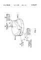
- FIG. 1diagrams how terms “relative crystallographic surface orientation” and “rotational alignment” are used in this disclosure
- FIG. 2is a graph of the voltage-current characteristics of two bonded compound semiconductor wafers of InGaP/GaP whose surface orientations are misaligned (Prior Art) and aligned using the teachings of the present invention;
- FIG. 3diagrams a specific case of "relative surface orientation” for nominally (100) oriented wafer surfaces
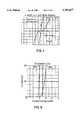
- FIG. 4is a graph of the voltage-current characteristics for isotype heterojunctions formed between bonded InGaP/GaP compound semiconductor wafers with varying degrees of rotational misalignment;
- FIG. 5diagrams a specific case of "rotational wafer alignment" for nominally (100) oriented wafer surfaces
- FIG. 6diagrams a specific case of 90° rotational wafer misalignment for nominally (100) oriented wafer surfaces
- FIG. 7is a graph of the voltage-current characteristics of two sets of InGaP/GaP bonded compound semiconductor wafers bonded with zero or 90° rotational misalignment
- FIG. 8further illustrates the effects of different alignments (Prior Art and Present Invention) in two sets of LEDs formed using bonded compound semiconductor wafers.
- FIG. 9illustrates how the present invention combined with the selective creation of areas of polycrystalline or amorphous regions in the wafers being bonded can create areas of conduction and non-conduction across the same interface.
- FIG. 1illustrates how these terms are used and described in this disclosure.
- Vector A sis normal to the surface of wafer A.
- Vector B shas the same crystallographic direction as vector A s , but within wafer B. All crystals are composed of a regular array of atoms which for the purposes of this disclosure can be visualized as consisting of various planar faces.
- the same crystallographic directionindicates that the planar face of the crystals in the second wafer corresponds to the same planar face of the first wafer.
- vector B smay project into wafer B at an angle.
- Wafer misorientationis the magnitude of the angle (
- a pis perpendicular to A s such that it lies in the plane of wafer A.
- Vector B pis the projection of the crystallographic direction of A p within wafer B into the plane of the surface of wafer B.
- Wafer misalignmentis the magnitude of the angle (
- Wafer rotational alignmentrefers to the matching of the direction of these vectors.
- the InGaP layers(-0.2-2 ⁇ m) are grown by metal organic chemical vapor deposition ("MOCVD") utilizing Te and Zn as the n-type and p-type dopants, respectively.
- MOCVDmetal organic chemical vapor deposition
- the In 0 .5 Ga 0 .5 P layersare grown lattice-matched on GaAs:Te (n>3 ⁇ 10 17 cm -3 ) or GaAs:Zn(p>1 ⁇ 10 18 cm -3 ) substrates whereas the In 0 .3 Ga 0 .7 P layers are grown lattice-mismatched on GaP:S (n>3 ⁇ 10 17 cm -3 ) substrates.
- All other materials discussed hereincomprise bulk compound semiconductor GaAs:Si, GaAs:Zn, GaP:S or GaP:Zn substrates with doping concentrations >3 ⁇ 10 17 cm -3 .
- the compound semiconductor wafer bondingis performed at elevated temperatures under applied uniaxial pressure in a graphite anvil fixture known in the art. In this disclosure, the accuracy of all angular tolerances and alignments specified is +/-0.5°.
- the present invention's teaching of proper surface orientation and rotational alignment matchinghas resulted in a substantial improvement in the electrical properties of the bonded interface between all the materials listed. These effects are due to the intrinsic crystal structure and the nature of the atomic bonding in compound semiconductors.
- the alignment and orientation matching methods taught hereinare thus applicable to all wafer bonding performed at high temperature under applied uniaxial pressure, which serves to recreate the crystal's chemical bonds, wherein at least one surface comprises a compound semiconductor.
- a first embodiment of the present inventionwas used to bond n-type (n>1 ⁇ 10 18 cm -3 ) In 0 .5 Ga 0 .5 P to n-type GaP (n>3 ⁇ 10 17 cm -3 ).
- All compound semiconductor wafer bonding of n-GaP to n-In 0 .5 Ga 0 .5 P in this and subsequent embodimentswas performed under identical conditions at 1000° C. The temperature was raised to this point over 40 minutes and was then immediately decreased back to room temperature over a 30 minute period. After the bonding operation was completed, full sheet alloyed ohmic contact metallizations were applied to both outer surfaces of the bonded wafers, which were then diced into 20 ⁇ 20 mil chips. All I-V characteristics for GaP/In 0 .5 Ga 0 .5 P isotype heterojunctions are measured by connecting the positive electrode to the GaP side of the junction.
- FIG. 2The effects of correct wafer orientation are illustrated by the I-V curves shown in FIG. 2.
- An n-type In 0 .5 Ga 0 .5 P layer with a (100)+2° toward (101) surface orientationwas bonded to an n-type GaP substrate with a surface orientation of either (100)+2° toward (101) in a first case or(100)+8° toward (101) in a second case.
- the I-V curves of the resultant junctionsare shown as curves 21 and 23 in FIG. 2, respectively.
- the wafersare rotationally aligned in both cases. An example of such alignment is shown in FIG. 3 which illustrates the 0 -1 -1!
- Low resistance ohmic conductioncan be achieved when bonding an n-In 0 .5 Ga 0 .5 P layer with a (100)+2° toward (101) surface orientation to an n-GaP substrate with a surface orientation of (100)+2° toward (110) (
- 2.83°).
- FIG. 4is a graph of the I-V performance of n-In 0 .5 Ga 0 .5 P layers wafer bonded to n-GaP substrates with different wafer rotational alignments. Both bonded layers have a surface orientation of (100)+2° toward (101).
- FIG. 5illustrates how the misalignment is measured and shows the misalignment of the 0 -1 -1! directions, indicated by the flats or cleavage planes at the wafers' edges by an angle of magnitude ⁇ degrees.
- the current conductionbecomes slightly non-linear and non-ohmic and the accompanying voltage drop across the heterojunction increases.
- the surface orientation of the layers forming the heterojunctionsis (100)+2° toward (101).
- )is less than the critical value of 6°.
- the primary natural cleavage planes for zinc blende crystalsare ⁇ 011 ⁇ planes.
- n-n heterojunctionsboth exhibit low resistance ohmic conduction similar to that shown by curve 41 in FIG. 4. Wafer misalignments of -20° ⁇ 20° or 160° ⁇ 200° will provide acceptable electrical characteristics for current conduction across the bonded interface with a minimal voltage drop.
- any of the above angles ⁇should produce a bonded interface that is capable of low resistance current conduction with a minimal accompanying voltage drop.
- nominally oriented (100) surfacespossess 180° rotational symmetry about the 001! and 010! directions.
- a nominally oriented (100) surfacemay be wafer bonded to any other surface obtained by rotating the (100) surface by 180° about these directions as long as the nominal surface orientations differ by less than 6° in magnitude and the relative alignment of the wafers in the plane of the bonding surfaces is within 20° of crystallographically equivalent directions.
- the magnitude of the relative misalignment of these "pseudo-surface" orientationsis constrained in a similar fashion to be less than 6°.
- the crystallographic directions in the plane of the wafer surfacesare then defined to be aligned when the atoms across the bonded interface are aligned as closely to that as found in a bulk crystalline semiconductor.
- the rotational alignmentis simultaneously constrained to be less than 20° in magnitude from any equivalent directions wherein the atoms across the bonded interface are aligned as closely as possible to that found in a bulk crystalline semiconductor.
- the techniques described hereinare generic to the bonding of at least one compound semiconductor to another semiconductor and are relatively independent of the lattice constant or doping types of the bonded surfaces. This has been demonstrated by bonding a p-type (p>1 ⁇ 10 18 cm -3 ) In 0 .5 Ga 0 .5 P layer oriented (100)+0.8° toward (110) to p-type (p>1 ⁇ 10 18 cm -3 ) In 0 .5 Ga 0 .5 P layers oriented either (100)+0.8° toward (110) or (100)+6° toward (110).
- the resistance of the bonded interface created by following the teachings of the present inventioncan be further decreased by using moderate to high doping levels (>3 ⁇ 10 17 cm -3 ). Merely increasing the doping concentration in the bonded surfaces without the teachings of the present invention does not eliminate the rectifying behavior of the interface and has been tried previously.
- the orientation matching taught hereinalso serves to maintain the crystal quality of the semiconductor crystal bordering the bonded interface.
- the low resistance compound semiconductor bonded interfaces capable of ohmic conduction that are formed by practicing the present inventionare valuable in many device applications.
- the present inventions's method for wafer bondinghas been shown to be a preferred method for fabricating high-efficiency transparent-substrate In 0 .5 (Al x Ga 1-x ) 0 .5 P LEDs. These LEDs are typically fabricated by selectively removing the absorbing n-type GaAs substrate upon which the device layers were initially grown. Next, an optically transparent n-type GaP substrate is wafer bonded in place of the GaAs, using the teachings of the present invention. This device design requires passing current across the wafer bonded interface while maintaining a low forward voltage.
- FIG. 8shows the I-V characteristics for semiconductor wafer bonded transparent substrate In 0 .5 (Al x Ga 1-x ) 0 .5 P LEDs with dimensions of 10.5 ⁇ 10.5 mills. All of the In 0 .5 (Al x Ga 1-x ) 0 .5 P epitaxial layers and the GaP substrates have surface orientations of (100)+2° toward (101). Both sets of LEDs whose performance is shown in FIG. 8 are fabricated under the same bonding and processing conditions with the exception of their wafer alignment.
- the I-V characteristics of curve 81 in FIG. 8are from a bonded LED wherein all of the crystallographic directions are aligned. These I-V curves exhibit a low forward voltage of -2.1 V at 20 mA.
- a high forward voltage(>3 V at 20 mA) results when the wafer alignment ( ⁇ ) has been allowed to differ by as much as 90° during fabrication. This is shown by curve 83. This high forward voltage is unacceptable in virtually all practical device implementations. Similar results were obtained but are not illustrated when the magnitude of the wafer's surface misorientation (
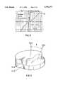
- polycrystalline or amorphous layers 91could be selectively patterned by laser melting and annealing or by ion implantation onto wafer bonding layers 93 and 95. Bonding of patterned layer 91 to another crystalline or patterned layer 93 results in low resistance ohmic conduction if the crystalline layers are aligned across the interface in the manner described and claimed herein. The regions where areas 91 have been deposited create non-ohmic contact areas. The method illustrated in FIG. 9 would be useful for defining paths of current flow in bonded structures.
Landscapes
- Engineering & Computer Science (AREA)
- Physics & Mathematics (AREA)
- Condensed Matter Physics & Semiconductors (AREA)
- General Physics & Mathematics (AREA)
- Manufacturing & Machinery (AREA)
- Computer Hardware Design (AREA)
- Microelectronics & Electronic Packaging (AREA)
- Power Engineering (AREA)
- Recrystallisation Techniques (AREA)
Abstract
Description
-20°+n120°<Θ<20°+n120°, |n|=0,1,2,
Claims (15)
Priority Applications (1)
| Application Number | Priority Date | Filing Date | Title |
|---|---|---|---|
| US08/835,948US5783477A (en) | 1996-09-20 | 1997-04-14 | Method for bonding compounds semiconductor wafers to create an ohmic interface |
Applications Claiming Priority (2)
| Application Number | Priority Date | Filing Date | Title |
|---|---|---|---|
| US08/718,223US5661316A (en) | 1994-01-18 | 1996-09-20 | Method for bonding compound semiconductor wafers to create an ohmic interface |
| US08/835,948US5783477A (en) | 1996-09-20 | 1997-04-14 | Method for bonding compounds semiconductor wafers to create an ohmic interface |
Related Parent Applications (1)
| Application Number | Title | Priority Date | Filing Date |
|---|---|---|---|
| US08/718,223DivisionUS5661316A (en) | 1994-01-18 | 1996-09-20 | Method for bonding compound semiconductor wafers to create an ohmic interface |
Publications (1)
| Publication Number | Publication Date |
|---|---|
| US5783477Atrue US5783477A (en) | 1998-07-21 |
Family
ID=24885282
Family Applications (1)
| Application Number | Title | Priority Date | Filing Date |
|---|---|---|---|
| US08/835,948Expired - LifetimeUS5783477A (en) | 1996-09-20 | 1997-04-14 | Method for bonding compounds semiconductor wafers to create an ohmic interface |
Country Status (1)
| Country | Link |
|---|---|
| US (1) | US5783477A (en) |
Cited By (28)
| Publication number | Priority date | Publication date | Assignee | Title |
|---|---|---|---|---|
| EP0994503A1 (en)* | 1998-10-16 | 2000-04-19 | Commissariat A L'energie Atomique | Structure comprising a thin layer composed of material containing conductive and isolation regions and method for manufacturing the structure |
| US6133071A (en)* | 1997-10-15 | 2000-10-17 | Nec Corporation | Semiconductor device with plate heat sink free from cracks due to thermal stress and process for assembling it with package |
| US6153495A (en)* | 1998-03-09 | 2000-11-28 | Intersil Corporation | Advanced methods for making semiconductor devices by low temperature direct bonding |
| WO2002013247A1 (en)* | 2000-08-09 | 2002-02-14 | Ziptronix, Inc. | A method of epitaxial-like wafer bonding at low temperature and bonded structure |
| EP1202355A2 (en)* | 2000-10-31 | 2002-05-02 | Kabushiki Kaisha Toshiba | Semiconductor light-emitting device and method of manufacturing the same |
| WO2002054466A1 (en)* | 2000-12-28 | 2002-07-11 | Commissariat A L'energie Atomique | Method for producing a stacked structure |
| US20020093023A1 (en)* | 1997-06-03 | 2002-07-18 | Camras Michael D. | III-Phosphide and III-Arsenide flip chip light-emitting devices |
| US6465809B1 (en) | 1999-06-09 | 2002-10-15 | Kabushiki Kaisha Toshiba | Bonding type semiconductor substrate, semiconductor light emitting element, and preparation process thereof |
| US6465803B1 (en) | 1996-05-07 | 2002-10-15 | The Regents Of The University Of California | Semiconductor hetero-interface photodetector |
| US6503359B2 (en) | 1999-03-05 | 2003-01-07 | Burstein Technologies, Inc. | Monomolecular adhesion methods for manufacturing microfabricated multilaminate devices |
| US20030211705A1 (en)* | 2000-02-16 | 2003-11-13 | Ziptronix, Inc. | Method for low temperature bonding and bonded structure |
| DE10244446A1 (en)* | 2002-09-24 | 2004-04-01 | Infineon Technologies Ag | Semiconductor chip or semiconductor chip stack |
| US20040195622A1 (en)* | 2003-04-07 | 2004-10-07 | United Microelectronics Corp. | Semiconductor structure with silicon on insulator |
| US6864585B2 (en) | 2000-03-22 | 2005-03-08 | Ziptronix, Inc. | Three dimensional device integration method and integrated device |
| US20050263776A1 (en)* | 2002-07-15 | 2005-12-01 | Min-Hsun Hsieh | Semiconductor light-emitting device and method for forming the same |
| US6984571B1 (en) | 1999-10-01 | 2006-01-10 | Ziptronix, Inc. | Three dimensional device integration method and integrated device |
| US20060172505A1 (en)* | 2005-01-31 | 2006-08-03 | Koester Steven J | Structure and method of integrating compound and elemental semiconductors for high-performace CMOS |
| US20060202215A1 (en)* | 2005-03-14 | 2006-09-14 | Lumileds Lighting U.S., Llc | Polarization-reversed III-nitride light emitting device |
| US20060202105A1 (en)* | 2005-03-14 | 2006-09-14 | Lumileds Lighting U.S., Llc | Wavelength-converted semiconductor light emitting device |
| US20070072391A1 (en)* | 2003-12-23 | 2007-03-29 | Commissariat A L'energie Atomique | Method of sealing two plates with the formation of an ohmic contact therebetween |
| US20070090491A1 (en)* | 2003-04-07 | 2007-04-26 | United Microelectronics Corp. | Semiconductor structure with silicon on insulator |
| EP1810948A1 (en)* | 2006-01-23 | 2007-07-25 | Commissariat A L'energie Atomique | Process to create an array of stress fields on a substrate for nucleation and growth of nanostructures |
| US20100283062A1 (en)* | 2003-07-04 | 2010-11-11 | Min-Hsun Hsieh | Optoelectronic system |
| US20110095325A1 (en)* | 2005-01-18 | 2011-04-28 | Epistar Corporation | Optoelectronic semiconductor device and manufacturing method thereof |
| US20110156056A1 (en)* | 2005-03-14 | 2011-06-30 | Philips Lumileds Lighting Company Llc | Wavelength-converted semiconductor light emitting device |
| EP2983220A3 (en)* | 2014-08-06 | 2016-03-09 | The Boeing Company | Solar cell wafer connecting system |
| US11760059B2 (en) | 2003-05-19 | 2023-09-19 | Adeia Semiconductor Bonding Technologies Inc. | Method of room temperature covalent bonding |
| US12424584B2 (en) | 2020-10-29 | 2025-09-23 | Adeia Semiconductor Bonding Technologies Inc. | Direct bonding methods and structures |
Citations (3)
| Publication number | Priority date | Publication date | Assignee | Title |
|---|---|---|---|---|
| US4315591A (en)* | 1979-03-08 | 1982-02-16 | General Electric Company | Method for thermo-compression diffusion bonding a structured copper strain buffer to each side of a substrateless semiconductor device wafer |
| US5236118A (en)* | 1992-05-12 | 1993-08-17 | The Regents Of The University Of California | Aligned wafer bonding |
| US5654583A (en)* | 1994-06-24 | 1997-08-05 | Hitachi, Ltd. | Semiconductor device having first and second semiconductor structures directly bonded to each other |
- 1997
- 1997-04-14USUS08/835,948patent/US5783477A/ennot_activeExpired - Lifetime
Patent Citations (3)
| Publication number | Priority date | Publication date | Assignee | Title |
|---|---|---|---|---|
| US4315591A (en)* | 1979-03-08 | 1982-02-16 | General Electric Company | Method for thermo-compression diffusion bonding a structured copper strain buffer to each side of a substrateless semiconductor device wafer |
| US5236118A (en)* | 1992-05-12 | 1993-08-17 | The Regents Of The University Of California | Aligned wafer bonding |
| US5654583A (en)* | 1994-06-24 | 1997-08-05 | Hitachi, Ltd. | Semiconductor device having first and second semiconductor structures directly bonded to each other |
Non-Patent Citations (4)
| Title |
|---|
| Okuno, Yae. "Investigation on Direct Bonding of III-V Semiconductor Wafers with Lattice Mismatch and Orientation Mismatch." Applied Physics Letters vol. 68, No. 20, May 13, 1996. |
| Okuno, Yae. Investigation on Direct Bonding of III V Semiconductor Wafers with Lattice Mismatch and Orientation Mismatch. Applied Physics Letters vol. 68, No. 20, May 13, 1996.* |
| Okuno, Yae; Uomi, Kaz; Aoki, Masahiro; Tsuchiya, Tomonobu. "Direct Wafer Bonding of III-V Compound Semiconductors for Free-Material and Fee Orientation Integration." IEEE Journal of Quantum Electronics, vol. 33, No. 6, Jun. 1997. |
| Okuno, Yae; Uomi, Kaz; Aoki, Masahiro; Tsuchiya, Tomonobu. Direct Wafer Bonding of III V Compound Semiconductors for Free Material and Fee Orientation Integration. IEEE Journal of Quantum Electronics, vol. 33, No. 6, Jun. 1997.* |
Cited By (83)
| Publication number | Priority date | Publication date | Assignee | Title |
|---|---|---|---|---|
| US6465803B1 (en) | 1996-05-07 | 2002-10-15 | The Regents Of The University Of California | Semiconductor hetero-interface photodetector |
| US20020093023A1 (en)* | 1997-06-03 | 2002-07-18 | Camras Michael D. | III-Phosphide and III-Arsenide flip chip light-emitting devices |
| US6784463B2 (en) | 1997-06-03 | 2004-08-31 | Lumileds Lighting U.S., Llc | III-Phospide and III-Arsenide flip chip light-emitting devices |
| US20040227148A1 (en)* | 1997-06-03 | 2004-11-18 | Camras Michael D. | III-Phosphide and III-Arsenide flip chip light-emitting devices |
| US7268371B2 (en) | 1997-06-03 | 2007-09-11 | Philips Lumileds Lighting Company, Llc | Light extraction from a semiconductor light emitting device via chip shaping |
| US6946309B2 (en) | 1997-06-03 | 2005-09-20 | Lumileds Lighting U.S., Llc | III-Phosphide and III-Arsenide flip chip light-emitting devices |
| US20060011935A1 (en)* | 1997-06-03 | 2006-01-19 | Krames Michael R | Light extraction from a semiconductor light emitting device via chip shaping |
| US6133071A (en)* | 1997-10-15 | 2000-10-17 | Nec Corporation | Semiconductor device with plate heat sink free from cracks due to thermal stress and process for assembling it with package |
| US6153495A (en)* | 1998-03-09 | 2000-11-28 | Intersil Corporation | Advanced methods for making semiconductor devices by low temperature direct bonding |
| EP0994503A1 (en)* | 1998-10-16 | 2000-04-19 | Commissariat A L'energie Atomique | Structure comprising a thin layer composed of material containing conductive and isolation regions and method for manufacturing the structure |
| US6362077B1 (en) | 1998-10-16 | 2002-03-26 | Commissariat A L'atomique | Structure comprising a thin layer of material made up of conductive zones and insulating zones and a method of manufacturing such a structure |
| FR2784795A1 (en)* | 1998-10-16 | 2000-04-21 | Commissariat Energie Atomique | STRUCTURE COMPRISING A THIN LAYER OF MATERIAL COMPOSED OF CONDUCTIVE ZONES AND INSULATING ZONES AND METHOD FOR MANUFACTURING SUCH A STRUCTURE |
| US20030136509A1 (en)* | 1999-03-05 | 2003-07-24 | Jorma Virtanen | Adhesion methods for manufacturing multilaminate devices |
| US6503359B2 (en) | 1999-03-05 | 2003-01-07 | Burstein Technologies, Inc. | Monomolecular adhesion methods for manufacturing microfabricated multilaminate devices |
| US6815312B2 (en) | 1999-06-09 | 2004-11-09 | Kabushiki Kaisha Toshiba | Bonding type semiconductor substrate, semiconductor light emitting element, and preparation process thereof |
| US6465809B1 (en) | 1999-06-09 | 2002-10-15 | Kabushiki Kaisha Toshiba | Bonding type semiconductor substrate, semiconductor light emitting element, and preparation process thereof |
| US20070111473A1 (en)* | 1999-06-09 | 2007-05-17 | Kabushiki Kaisha Toshiba | Process for preparing a bonding type semiconductor substrate |
| US8829488B2 (en) | 1999-06-09 | 2014-09-09 | Kabushiki Kaisha Toshiba | Process for preparing a bonding type semiconductor substrate |
| US20050066880A1 (en)* | 1999-06-09 | 2005-03-31 | Kabushiki Kaisha Toshiba | Process for preparing a bonding type semiconductor substrate |
| US20020185648A1 (en)* | 1999-06-09 | 2002-12-12 | Kabushiki Kaisha Toshiba | Bonding type semiconductor substrate, semiconductor light emitting element, and preparation process thereof |
| US7364982B2 (en) | 1999-06-09 | 2008-04-29 | Kabushiki Kaisha Toshiba | Process for preparing a bonding type semiconductor substrate |
| US10366962B2 (en) | 1999-10-01 | 2019-07-30 | Invensas Bonding Technologies, Inc. | Three dimensional device integration method and integrated device |
| US9564414B2 (en) | 1999-10-01 | 2017-02-07 | Ziptronix, Inc. | Three dimensional device integration method and integrated device |
| US6984571B1 (en) | 1999-10-01 | 2006-01-10 | Ziptronix, Inc. | Three dimensional device integration method and integrated device |
| US9431368B2 (en) | 1999-10-01 | 2016-08-30 | Ziptronix, Inc. | Three dimensional device integration method and integrated device |
| US7041178B2 (en) | 2000-02-16 | 2006-05-09 | Ziptronix, Inc. | Method for low temperature bonding and bonded structure |
| US9082627B2 (en) | 2000-02-16 | 2015-07-14 | Ziptronix, Inc. | Method for low temperature bonding and bonded structure |
| US7387944B2 (en) | 2000-02-16 | 2008-06-17 | Ziptronix, Inc. | Method for low temperature bonding and bonded structure |
| US20050079712A1 (en)* | 2000-02-16 | 2005-04-14 | Ziptronix, Inc. | Method for low temperature bonding and bonded structure |
| US7335572B2 (en) | 2000-02-16 | 2008-02-26 | Ziptronix, Inc. | Method for low temperature bonding and bonded structure |
| US6902987B1 (en) | 2000-02-16 | 2005-06-07 | Ziptronix, Inc. | Method for low temperature bonding and bonded structure |
| US20090263953A1 (en)* | 2000-02-16 | 2009-10-22 | Ziptronix, Inc. | Method for low temperature bonding and bonded structure |
| US20040152282A1 (en)* | 2000-02-16 | 2004-08-05 | Ziptronix, Inc. | Method for low temperature bonding and bonded structure |
| US10312217B2 (en) | 2000-02-16 | 2019-06-04 | Invensas Bonding Technologies, Inc. | Method for low temperature bonding and bonded structure |
| US8053329B2 (en) | 2000-02-16 | 2011-11-08 | Ziptronix, Inc. | Method for low temperature bonding and bonded structure |
| US8153505B2 (en) | 2000-02-16 | 2012-04-10 | Ziptronix, Inc. | Method for low temperature bonding and bonded structure |
| US9391143B2 (en) | 2000-02-16 | 2016-07-12 | Ziptronix, Inc. | Method for low temperature bonding and bonded structure |
| US9331149B2 (en) | 2000-02-16 | 2016-05-03 | Ziptronix, Inc. | Method for low temperature bonding and bonded structure |
| US20030211705A1 (en)* | 2000-02-16 | 2003-11-13 | Ziptronix, Inc. | Method for low temperature bonding and bonded structure |
| US6864585B2 (en) | 2000-03-22 | 2005-03-08 | Ziptronix, Inc. | Three dimensional device integration method and integrated device |
| US6563133B1 (en)* | 2000-08-09 | 2003-05-13 | Ziptronix, Inc. | Method of epitaxial-like wafer bonding at low temperature and bonded structure |
| WO2002013247A1 (en)* | 2000-08-09 | 2002-02-14 | Ziptronix, Inc. | A method of epitaxial-like wafer bonding at low temperature and bonded structure |
| US20030141502A1 (en)* | 2000-08-09 | 2003-07-31 | Ziptronix | Method of epitaxial-like wafer bonding at low temperature and bonded structure |
| US7332410B2 (en) | 2000-08-09 | 2008-02-19 | Ziptronix, Inc. | Method of epitaxial-like wafer bonding at low temperature and bonded structure |
| US20030201449A1 (en)* | 2000-10-31 | 2003-10-30 | Ryo Saeki | Semiconductor light-emitting device and method of manufacturing the same |
| EP1202355A2 (en)* | 2000-10-31 | 2002-05-02 | Kabushiki Kaisha Toshiba | Semiconductor light-emitting device and method of manufacturing the same |
| US6846686B2 (en)* | 2000-10-31 | 2005-01-25 | Kabushiki Kaisha Toshiba | Semiconductor light-emitting device and method of manufacturing the same |
| US7229897B2 (en)* | 2000-12-28 | 2007-06-12 | Commissariat A L'energie Atomique | Method for producing a stacked structure |
| WO2002054466A1 (en)* | 2000-12-28 | 2002-07-11 | Commissariat A L'energie Atomique | Method for producing a stacked structure |
| US20050101095A1 (en)* | 2000-12-28 | 2005-05-12 | Franck Fournel | Method for producing a stacked structure |
| US20110156078A1 (en)* | 2002-07-15 | 2011-06-30 | Min-Hsun Hsieh | Semiconductor light-emitting device and method for forming the same |
| US7928455B2 (en) | 2002-07-15 | 2011-04-19 | Epistar Corporation | Semiconductor light-emitting device and method for forming the same |
| US8853722B2 (en) | 2002-07-15 | 2014-10-07 | Epistar Corporation | Semiconductor light-emitting device and method for forming the same |
| US20050263776A1 (en)* | 2002-07-15 | 2005-12-01 | Min-Hsun Hsieh | Semiconductor light-emitting device and method for forming the same |
| DE10244446B4 (en)* | 2002-09-24 | 2004-08-19 | Infineon Technologies Ag | Semiconductor chip stack |
| DE10244446A1 (en)* | 2002-09-24 | 2004-04-01 | Infineon Technologies Ag | Semiconductor chip or semiconductor chip stack |
| US20040195622A1 (en)* | 2003-04-07 | 2004-10-07 | United Microelectronics Corp. | Semiconductor structure with silicon on insulator |
| US20070090491A1 (en)* | 2003-04-07 | 2007-04-26 | United Microelectronics Corp. | Semiconductor structure with silicon on insulator |
| US11760059B2 (en) | 2003-05-19 | 2023-09-19 | Adeia Semiconductor Bonding Technologies Inc. | Method of room temperature covalent bonding |
| US9748449B2 (en) | 2003-07-04 | 2017-08-29 | Epistar Corporation | Optoelectronic system |
| US20100283062A1 (en)* | 2003-07-04 | 2010-11-11 | Min-Hsun Hsieh | Optoelectronic system |
| US8999736B2 (en) | 2003-07-04 | 2015-04-07 | Epistar Corporation | Optoelectronic system |
| US20070072391A1 (en)* | 2003-12-23 | 2007-03-29 | Commissariat A L'energie Atomique | Method of sealing two plates with the formation of an ohmic contact therebetween |
| US8975156B2 (en)* | 2003-12-23 | 2015-03-10 | Commissariat A L'energie Atomique | Method of sealing two plates with the formation of an ohmic contact therebetween |
| US8860065B2 (en) | 2005-01-18 | 2014-10-14 | Epistar Corporation | Optoelectronic semiconductor device |
| US20110095325A1 (en)* | 2005-01-18 | 2011-04-28 | Epistar Corporation | Optoelectronic semiconductor device and manufacturing method thereof |
| US20060172505A1 (en)* | 2005-01-31 | 2006-08-03 | Koester Steven J | Structure and method of integrating compound and elemental semiconductors for high-performace CMOS |
| US7282425B2 (en)* | 2005-01-31 | 2007-10-16 | International Business Machines Corporation | Structure and method of integrating compound and elemental semiconductors for high-performance CMOS |
| US7804100B2 (en) | 2005-03-14 | 2010-09-28 | Philips Lumileds Lighting Company, Llc | Polarization-reversed III-nitride light emitting device |
| US20110156056A1 (en)* | 2005-03-14 | 2011-06-30 | Philips Lumileds Lighting Company Llc | Wavelength-converted semiconductor light emitting device |
| US20060202105A1 (en)* | 2005-03-14 | 2006-09-14 | Lumileds Lighting U.S., Llc | Wavelength-converted semiconductor light emitting device |
| US7341878B2 (en) | 2005-03-14 | 2008-03-11 | Philips Lumileds Lighting Company, Llc | Wavelength-converted semiconductor light emitting device |
| US20060202215A1 (en)* | 2005-03-14 | 2006-09-14 | Lumileds Lighting U.S., Llc | Polarization-reversed III-nitride light emitting device |
| US8445929B2 (en) | 2005-03-14 | 2013-05-21 | Philips Lumileds Lighting Company Llc | Wavelength-converted semiconductor light emitting device |
| US20100200886A1 (en)* | 2005-03-14 | 2010-08-12 | Koninklijke Philips Electronics N.V. | Wavelength-converted semiconductor light emitting device |
| US8748923B2 (en) | 2005-03-14 | 2014-06-10 | Philips Lumileds Lighting Company Llc | Wavelength-converted semiconductor light emitting device |
| US20080121919A1 (en)* | 2005-03-14 | 2008-05-29 | Philips Lumileds Lighting Company Llc | Wavelength-Converted Semiconductor Light Emitting Device |
| FR2896493A1 (en)* | 2006-01-23 | 2007-07-27 | Commissariat Energie Atomique | METHOD FOR PRODUCING A SUPPORT FOR THE GROWTH OF LOCALIZED LONG NANOSTRUCTURES |
| EP1810948A1 (en)* | 2006-01-23 | 2007-07-25 | Commissariat A L'energie Atomique | Process to create an array of stress fields on a substrate for nucleation and growth of nanostructures |
| US11245060B2 (en) | 2007-08-27 | 2022-02-08 | Epistar Corporation | Optoelectronic semiconductor device |
| US9425331B2 (en) | 2014-08-06 | 2016-08-23 | The Boeing Company | Solar cell wafer connecting system |
| EP2983220A3 (en)* | 2014-08-06 | 2016-03-09 | The Boeing Company | Solar cell wafer connecting system |
| US12424584B2 (en) | 2020-10-29 | 2025-09-23 | Adeia Semiconductor Bonding Technologies Inc. | Direct bonding methods and structures |
Similar Documents
| Publication | Publication Date | Title |
|---|---|---|
| US5661316A (en) | Method for bonding compound semiconductor wafers to create an ohmic interface | |
| US5783477A (en) | Method for bonding compounds semiconductor wafers to create an ohmic interface | |
| CA1299068C (en) | Semiconductor deposition method and device | |
| EP2647034B1 (en) | Direct wafer bonding | |
| US5502316A (en) | Wafer bonding of light emitting diode layers | |
| US20080296619A1 (en) | Adhesive bonding with low temperature grown amorphous or polycrystalline compound semiconductors | |
| US5838029A (en) | GaN-type light emitting device formed on a silicon substrate | |
| US7622398B2 (en) | Semiconductor device, semiconductor layer and production method thereof | |
| US4697202A (en) | Integrated circuit having dislocation free substrate | |
| Beneking et al. | High quality epitaxial GaAs and InP wafers by isoelectronic doping | |
| KR102481927B1 (en) | Compound semiconductor laminated substrate, manufacturing method thereof, and semiconductor device | |
| JPH0770474B2 (en) | Method for manufacturing compound semiconductor device | |
| JP2005508077A (en) | Method of hyperdoping semiconductor material, hyperdoped semiconductor material, and hyperdoped semiconductor device | |
| Tsutsui et al. | Optimum growth conditions of GaAs (111) B layers for good electrical properties by molecular beam epitaxy | |
| US20090072353A1 (en) | Method for increasing the area of non-polar and semi-polar nitride substrates | |
| Faurie et al. | Molecular beam epitaxial growth of high quality HgTe and Hg1− x Cd x Te onto GaAs (001) substrates | |
| US5365533A (en) | Integrated circuit of semiconductor lasers | |
| Vanderwater et al. | Electrical conduction through compound semiconductor wafer bonded interfaces | |
| JP6996436B2 (en) | Layered material laminated structure and its manufacturing method | |
| KR100425092B1 (en) | method for fabricating silicon compliant substrate | |
| Namkoong et al. | III-NITRIDE FILMS AND DEVICES ON LITHIUM METAL OXIDES BY MOLECULAR BEAM EPITAXY | |
| JPH1064828A (en) | Nitride semiconductor crystal structure | |
| JPH03161987A (en) | Semiconductor laser device | |
| CN1938821A (en) | Compound semiconductor element, manufacturing method of compound semiconductor element, diode element | |
| Phillips et al. | Growth of ZnTe and ZnSexTe1-x epilayers and superlattices on GaSb |
Legal Events
| Date | Code | Title | Description |
|---|---|---|---|
| STCF | Information on status: patent grant | Free format text:PATENTED CASE | |
| AS | Assignment | Owner name:HEWLETT-PACKARD COMPANY, A CORP. OF DELAWARE, COLO Free format text:CHANGE OF NAME;ASSIGNOR:HEWLETT-PACKARD COMPANY;REEL/FRAME:010668/0728 Effective date:19980520 | |
| AS | Assignment | Owner name:HEWLETT-PACKARD COMPANY, A DELAWARE CORPORATION, C Free format text:MERGER;ASSIGNOR:HEWLETT-PACKARD COMPANY, A CALIFORNIA CORPORATION;REEL/FRAME:010841/0649 Effective date:19980520 | |
| AS | Assignment | Owner name:AGILENT TECHNOLOGIES INC, CALIFORNIA Free format text:ASSIGNMENT OF ASSIGNORS INTEREST;ASSIGNOR:HEWLETT-PACKARD COMPANY;REEL/FRAME:010977/0540 Effective date:19991101 | |
| AS | Assignment | Owner name:LUMILEDS LIGHTING, U.S., LLC, CALIFORNIA Free format text:ASSIGNMENT OF ASSIGNORS INTEREST;ASSIGNOR:AGILENT TECHNOLOGIES, INC.;REEL/FRAME:011170/0223 Effective date:20000906 | |
| FPAY | Fee payment | Year of fee payment:4 | |
| REMI | Maintenance fee reminder mailed | ||
| FPAY | Fee payment | Year of fee payment:8 | |
| FPAY | Fee payment | Year of fee payment:12 | |
| AS | Assignment | Owner name:PHILIPS LUMILEDS LIGHTING COMPANY LLC, CALIFORNIA Free format text:CHANGE OF NAME;ASSIGNORS:LUMILEDS LIGHTING U.S., LLC;LUMILEDS LIGHTING, U.S., LLC;LUMILEDS LIGHTING, U.S. LLC;AND OTHERS;REEL/FRAME:025850/0770 Effective date:20110211 | |
| AS | Assignment | Owner name:DEUTSCHE BANK AG NEW YORK BRANCH, AS COLLATERAL AGENT, NEW YORK Free format text:SECURITY INTEREST;ASSIGNOR:LUMILEDS LLC;REEL/FRAME:043108/0001 Effective date:20170630 Owner name:DEUTSCHE BANK AG NEW YORK BRANCH, AS COLLATERAL AG Free format text:SECURITY INTEREST;ASSIGNOR:LUMILEDS LLC;REEL/FRAME:043108/0001 Effective date:20170630 | |
| AS | Assignment | Owner name:LUMILEDS LLC, CALIFORNIA Free format text:CHANGE OF NAME;ASSIGNOR:PHILIPS LUMILEDS LIGHTING COMPANY, LLC;REEL/FRAME:046111/0261 Effective date:20150326 |