US5781587A - Clock extraction circuit - Google Patents
Clock extraction circuitDownload PDFInfo
- Publication number
- US5781587A US5781587AUS08/553,106US55310695AUS5781587AUS 5781587 AUS5781587 AUS 5781587AUS 55310695 AUS55310695 AUS 55310695AUS 5781587 AUS5781587 AUS 5781587A
- Authority
- US
- United States
- Prior art keywords
- stream
- binary
- retimed
- clock
- retiming
- Prior art date
- Legal status (The legal status is an assumption and is not a legal conclusion. Google has not performed a legal analysis and makes no representation as to the accuracy of the status listed.)
- Expired - Lifetime
Links
Images


Classifications
- H—ELECTRICITY
- H04—ELECTRIC COMMUNICATION TECHNIQUE
- H04L—TRANSMISSION OF DIGITAL INFORMATION, e.g. TELEGRAPHIC COMMUNICATION
- H04L7/00—Arrangements for synchronising receiver with transmitter
- H04L7/0054—Detection of the synchronisation error by features other than the received signal transition
- H04L7/0066—Detection of the synchronisation error by features other than the received signal transition detection of error based on transmission code rule
- H—ELECTRICITY
- H04—ELECTRIC COMMUNICATION TECHNIQUE
- H04L—TRANSMISSION OF DIGITAL INFORMATION, e.g. TELEGRAPHIC COMMUNICATION
- H04L7/00—Arrangements for synchronising receiver with transmitter
- H04L7/0079—Receiver details
- H04L7/0083—Receiver details taking measures against momentary loss of synchronisation, e.g. inhibiting the synchronisation, using idle words or using redundant clocks
- H—ELECTRICITY
- H04—ELECTRIC COMMUNICATION TECHNIQUE
- H04L—TRANSMISSION OF DIGITAL INFORMATION, e.g. TELEGRAPHIC COMMUNICATION
- H04L7/00—Arrangements for synchronising receiver with transmitter
- H04L7/02—Speed or phase control by the received code signals, the signals containing no special synchronisation information
- H04L7/033—Speed or phase control by the received code signals, the signals containing no special synchronisation information using the transitions of the received signal to control the phase of the synchronising-signal-generating means, e.g. using a phase-locked loop
Definitions
- This inventionrelates to digital transmission systems and in particular to clock extraction arrangements for such systems.
- the inventionalso relates to multiplexers/demultiplexers incorporating such clock extraction arrangements.
- a key feature of any digital transmission system in which a plurality of signals are multiplexed and demultiplexedis the provision of some means of synchronisation to ensure that the timing of transmission equipment such as a multiplexer/demultiplexer is matched to the signal timing.
- this ⁇ local ⁇ synchronisationis achieved by extracting timing or clock information from the digital signal itself.
- phase locked loopprovides a substantially jitter-free ⁇ flywheel ⁇ synchronisation with a received digital signal.
- a typical phase locked loop techniqueis described in specification GB-A-2,255,480. While this technique provides an effective solution, the circuitry required is complex and is thus relatively costly.
- the object of the inventionis to minimise or to overcome this disadvantage.
- a clock extraction circuitfor a digital transmission system and adapted to extract timing information from a ternary data pulse stream whereby to retime the ternary data stream
- the circuitincluding means for deriving first and second binary signal streams corresponding respectively to the positive and negative going pulses of the ternary data stream, means for combining said first and second binary streams to provide a further binary stream, means including a local clock for generating from said further binary stream a reference signal stream, means for retiming said first and second binary data streams to said reference signal stream, and means for recombining said retimed binary data streams whereby to generate a retimed ternary data stream, characterised in that the reference signal stream is generated by retiming the further binary stream to the local clock, delaying the retimed further binary stream by one clock pulse, and combining the delayed binary stream with the further binary stream to provide a twice bit rate clock signal whose rising edges are aligned to the further binary stream and provide a timing reference for retiming said
- a method of retiming a ternary data signal in a digital transmission systemincluding deriving first and second binary signal streams corresponding respectively to the positive and negative going pulses of the ternary data stream, combining said first and second binary streams to provide a further binary stream, generating from said further binary stream and from a local clock a reference signal stream, retiming said first and second binary data streams to said reference signal stream, and recombining said retimed binary data streams whereby to generate a retimed ternary data stream, characterised in that the reference signal stream is generated by retiming the further binary stream to the local clock, delaying the retimed further binary stream by one clock pulse, and combining the delayed binary stream with the further binary stream to provide a twice bit rate clock signal whose rising edges are aligned to the further binary stream and provide a timing reference for retiming said first and second binary signals.
- the circuitmay be employed for the retiming of ternary data in a digital repeater.
- FIG. 1is a schematic diagram of a digital multiplexer/demultiplexer arrangement
- FIG. 2shows in schematic form a digital processor for use in the multiplexer/demultiplexer arrangement of FIG. 1;
- FIG. 3shows a clock extraction circuit for use in the processor of FIG. 2;
- FIGS. 4 and 5illustrate signal wave forms for the circuit of FIG. 3.
- the multiplexer/demultiplexer arrangementincludes a digital processor 11 coupled to a set of tributary inputs 110 and tributary outputs 111.
- the tributariescomprise wired inputs and outputs and carry data at a rate of 2 Mb/s.
- the processor 11is also coupled to a pair of optical line transmission units (OLTU 1 and OLTU 2) which provide an interface to an optical transmission network 12 comprising e.g. a passive optical network. In use, only one of the line transmission units is enabled at any one time, the other unit providing a back-up in case of a system failure.
- the processoris shown in further detail in FIG. 2 and includes means for regenerating (21) and retiming (22) ternary, e.g. HDB3 encoded data from the tributary input or from the line termination units.
- the regenerator 21outputs two binary signal streams DP and DN corresponding respectively to the positive going and negative going pulses of the ternary data stream. These signals are fed to clock extraction circuit 22 via NAND gate 31 and to respective flip-flops 23P and 23N whose clock inputs receive timing information from the retiming means or clock extraction circuit 22.
- the retimed HDB3 signalsare output in parallel to a pair of output buffers 24A and 24B.
- the processoraccepts four tributary input signals from the served equipment and regenerates and retimes the data whereby to provide two identical copies of the input data stream for transmission to the network.
- Alarmssuch as loss of input signal, AIS present and HDB3 coding errors are extracted from the input data streams.
- the processoraccepts eight inputs from the receive sides of the optical line termination units. The alarms are collected from these data streams and, optionally the processor may search for frame alignment and for framing errors.
- the tributary outputsare switched either individually or as a block of four.
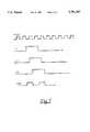
- the clock extraction circuit 22is shown in FIG. 3 and the associated signal waveforms in FIGS. 4 and 5. To facilitate the understanding of the technique, the time axis of FIG. 5 is compressed relative to that of FIG. 4.
- the positive going and negative going portions of the HDB3 data streamare used to generate respective data streams DP and DN. These data streams are combined by NAND gate 31 (FIG. 3) to provide a single data stream D (FIG. 4).
- This data stream Dis then retimed (FIG. 5) using the external clock SLCLK to generate a waveforms R1 which is timed to the next positive going clock pulse and a second wave form R2 which is delayed by one clock pulse after R1.
- waveforms R2can be generated directly, it is more convenient to generate this wave form indirectly from R1.
- the waveforms D and R2are then combined in XOR gate 32 (FIG. 3) producing a twice bit rate clock (FIG. 5) whose rising edges are aligned to the data stream and which can be used to retime the input data stream.
- the falling edges of the XOR outputare aligned to the standby clock so that the clock pulse will have a mark/space ratio within set limits.
- the falling edgeswill be subject to jitter as they are not related to the data frequency, but this is no disadvantage as the falling edges are not used in the retiming process.
- the gapped clock produced at the XOR gate outputis used to continually reset the counter 33 (FIG. 3).
- this clockis not related to the data stream, no jitter is added as the zeros or spaces do not contain any timing information. There is no necessary to decode the retimed data before it is applied to the output buffers 24A and 24B (FIG. 2) to provide a broadcast transmit facility.
Landscapes
- Engineering & Computer Science (AREA)
- Computer Networks & Wireless Communication (AREA)
- Signal Processing (AREA)
- Time-Division Multiplex Systems (AREA)
- Synchronisation In Digital Transmission Systems (AREA)
Abstract
Description
Claims (6)
Applications Claiming Priority (2)
| Application Number | Priority Date | Filing Date | Title |
|---|---|---|---|
| GB9422233AGB2294850B (en) | 1994-11-03 | 1994-11-03 | Clock extraction circuit |
| GB9422233 | 1994-11-03 |
Publications (1)
| Publication Number | Publication Date |
|---|---|
| US5781587Atrue US5781587A (en) | 1998-07-14 |
Family
ID=10763870
Family Applications (1)
| Application Number | Title | Priority Date | Filing Date |
|---|---|---|---|
| US08/553,106Expired - LifetimeUS5781587A (en) | 1994-11-03 | 1995-11-03 | Clock extraction circuit |
Country Status (4)
| Country | Link |
|---|---|
| US (1) | US5781587A (en) |
| DE (1) | DE19541065A1 (en) |
| FR (1) | FR2726714B1 (en) |
| GB (1) | GB2294850B (en) |
Cited By (3)
| Publication number | Priority date | Publication date | Assignee | Title |
|---|---|---|---|---|
| US6338156B1 (en)* | 1997-12-23 | 2002-01-08 | Alcatel | Method and device for detecting the loss-of-signal condition at the input of a transmission line interface |
| US6680988B1 (en)* | 1999-08-13 | 2004-01-20 | Oki Electric Industry Co., Ltd. | Non-linear extraction circuit and clock extraction circuit |
| JP2014239363A (en)* | 2013-06-10 | 2014-12-18 | 株式会社明電舎 | Received clock extraction circuit |
Families Citing this family (3)
| Publication number | Priority date | Publication date | Assignee | Title |
|---|---|---|---|---|
| RU2121763C1 (en)* | 1995-10-23 | 1998-11-10 | Акционерное общество открытого типа "Информационные телекоммуникационные технологии" | Method for transmitting and receiving digital information |
| DE10005152A1 (en)* | 2000-02-07 | 2001-08-09 | Deutsche Telekom Mobil | Method for regenerating a clock signal from an HDB3-coded input signal and clock regenerator for performing the method |
| RU2356088C1 (en)* | 2008-03-11 | 2009-05-20 | Общество с ограниченной ответственностью НПЦ "Динамика" - Научно-производственный центр "Диагностика, надежность машин и комплексная автоматизация" | Device for remote input-output of discrete signals with galvanic isolation |
Citations (8)
| Publication number | Priority date | Publication date | Assignee | Title |
|---|---|---|---|---|
| US4456890A (en)* | 1982-04-05 | 1984-06-26 | Computer Peripherals Inc. | Data tracking clock recovery system using digitally controlled oscillator |
| US5056118A (en)* | 1989-05-16 | 1991-10-08 | Rockwell International Corporation | Method and apparatus for clock and data recovery with high jitter tolerance |
| GB2255480A (en)* | 1991-04-23 | 1992-11-04 | Motorola Israel Ltd | A data demodulator |
| GB2259632A (en)* | 1991-09-13 | 1993-03-17 | Al Sammak Abdul Imam Jassim | An encoder/decoder for Manchester code |
| GB2260883A (en)* | 1991-10-24 | 1993-04-28 | Northern Telecom Ltd | Clock recovery from a Manchester encoded frame |
| GB2263609A (en)* | 1991-09-30 | 1993-07-28 | Plessey Telecomm | Clock extract circuit |
| GB2271492A (en)* | 1992-03-26 | 1994-04-13 | Motorola Inc | Apparatus for and method of synchronizing a clock signal |
| US5455540A (en)* | 1994-10-26 | 1995-10-03 | Cypress Semiconductor Corp. | Modified bang-bang phase detector with ternary output |
Family Cites Families (3)
| Publication number | Priority date | Publication date | Assignee | Title |
|---|---|---|---|---|
| US4284843A (en)* | 1979-05-10 | 1981-08-18 | General Electric Company | Repeating station for use in digital data communications link |
| US4696016A (en)* | 1986-10-02 | 1987-09-22 | Rockwell International Corporation | Digital clock recovery circuit for return to zero data |
| FR2646742B1 (en)* | 1989-05-03 | 1994-01-07 | Telecommunications Sa | DEVICE FOR SYNCHRONIZING A PSEUDO-BINARY SIGNAL WITH A REGENERATED CLOCK SIGNAL WITH PHASE JUMPS |
- 1994
- 1994-11-03GBGB9422233Apatent/GB2294850B/ennot_activeExpired - Fee Related
- 1995
- 1995-11-03USUS08/553,106patent/US5781587A/ennot_activeExpired - Lifetime
- 1995-11-03FRFR9512998Apatent/FR2726714B1/ennot_activeExpired - Fee Related
- 1995-11-03DEDE19541065Apatent/DE19541065A1/ennot_activeWithdrawn
Patent Citations (8)
| Publication number | Priority date | Publication date | Assignee | Title |
|---|---|---|---|---|
| US4456890A (en)* | 1982-04-05 | 1984-06-26 | Computer Peripherals Inc. | Data tracking clock recovery system using digitally controlled oscillator |
| US5056118A (en)* | 1989-05-16 | 1991-10-08 | Rockwell International Corporation | Method and apparatus for clock and data recovery with high jitter tolerance |
| GB2255480A (en)* | 1991-04-23 | 1992-11-04 | Motorola Israel Ltd | A data demodulator |
| GB2259632A (en)* | 1991-09-13 | 1993-03-17 | Al Sammak Abdul Imam Jassim | An encoder/decoder for Manchester code |
| GB2263609A (en)* | 1991-09-30 | 1993-07-28 | Plessey Telecomm | Clock extract circuit |
| GB2260883A (en)* | 1991-10-24 | 1993-04-28 | Northern Telecom Ltd | Clock recovery from a Manchester encoded frame |
| GB2271492A (en)* | 1992-03-26 | 1994-04-13 | Motorola Inc | Apparatus for and method of synchronizing a clock signal |
| US5455540A (en)* | 1994-10-26 | 1995-10-03 | Cypress Semiconductor Corp. | Modified bang-bang phase detector with ternary output |
Cited By (3)
| Publication number | Priority date | Publication date | Assignee | Title |
|---|---|---|---|---|
| US6338156B1 (en)* | 1997-12-23 | 2002-01-08 | Alcatel | Method and device for detecting the loss-of-signal condition at the input of a transmission line interface |
| US6680988B1 (en)* | 1999-08-13 | 2004-01-20 | Oki Electric Industry Co., Ltd. | Non-linear extraction circuit and clock extraction circuit |
| JP2014239363A (en)* | 2013-06-10 | 2014-12-18 | 株式会社明電舎 | Received clock extraction circuit |
Also Published As
| Publication number | Publication date |
|---|---|
| GB9422233D0 (en) | 1994-12-21 |
| FR2726714B1 (en) | 2000-08-11 |
| GB2294850B (en) | 1999-01-13 |
| FR2726714A1 (en) | 1996-05-10 |
| DE19541065A1 (en) | 1996-05-09 |
| GB2294850A (en) | 1996-05-08 |
Similar Documents
| Publication | Publication Date | Title |
|---|---|---|
| EP0477582B1 (en) | Digital frequency multiplication and data serialization circuits | |
| US6449315B2 (en) | Serial line synchronization method and apparatus | |
| CA1298420C (en) | Demultiplexer system | |
| US4891808A (en) | Self-synchronizing multiplexer | |
| US6628679B1 (en) | SERDES (serializer/deserializer) time domain multiplexing/demultiplexing technique | |
| CA1309194C (en) | High speed digital signal framer-demultiplexer | |
| US6288656B1 (en) | Receive deserializer for regenerating parallel data serially transmitted over multiple channels | |
| US5442636A (en) | Circuit and method for alignment of digital information packets | |
| JPS60182833A (en) | Clock recovering device in ring type data communication circuit network | |
| US5081619A (en) | Digital signal multiplex communication system having signal path monitoring function | |
| US9143420B2 (en) | Data transport system, receiver and transmitter | |
| US5781587A (en) | Clock extraction circuit | |
| CN101621346B (en) | Source synchronous receiving device with adaptive feedback and source synchronizing method | |
| US4010325A (en) | Framing circuit for digital signals using evenly spaced alternating framing bits | |
| US7058090B1 (en) | System and method for paralleling digital wrapper data streams | |
| US5430733A (en) | Digital transmission system for multiplexing and demultiplexing signals | |
| EP0197492A2 (en) | A method and an apparatus for modeling bit rate justification | |
| JP2693466B2 (en) | Multiplex code conversion method | |
| KR100204062B1 (en) | Slow Data Frame Phase Aligner | |
| JP2693831B2 (en) | Auxiliary signal transmission method | |
| JPH11239121A (en) | Digital communications equipment | |
| JPH03149931A (en) | Phase synchronizing circuit between parallel signals | |
| JP2713009B2 (en) | Delay time difference absorption device | |
| JPS5816772B2 (en) | Synchronization method | |
| JPH03145834A (en) | timing extraction circuit |
Legal Events
| Date | Code | Title | Description |
|---|---|---|---|
| AS | Assignment | Owner name:HITACHI, LTD., JAPAN Free format text:ASSIGNMENT OF ASSIGNORS INTEREST;ASSIGNORS:OSAKA, HIDEKI;YAMAGIWA, AKIRA;KURIHARA, RYOICHI;AND OTHERS;REEL/FRAME:007787/0598 Effective date:19951108 | |
| AS | Assignment | Owner name:NORTHERN TELECOM LIMITED, CANADA Free format text:ASSIGNMENT OF ASSIGNORS INTEREST;ASSIGNOR:BRUCE, PAUL;REEL/FRAME:007785/0213 Effective date:19951206 | |
| STCF | Information on status: patent grant | Free format text:PATENTED CASE | |
| AS | Assignment | Owner name:NORTEL NETWORKS CORPORATION, CANADA Free format text:CHANGE OF NAME;ASSIGNOR:NORTHERN TELECOM LIMITED;REEL/FRAME:010567/0001 Effective date:19990429 | |
| AS | Assignment | Owner name:NORTEL NETWORKS LIMITED, CANADA Free format text:CHANGE OF NAME;ASSIGNOR:NORTEL NETWORKS CORPORATION;REEL/FRAME:011195/0706 Effective date:20000830 Owner name:NORTEL NETWORKS LIMITED,CANADA Free format text:CHANGE OF NAME;ASSIGNOR:NORTEL NETWORKS CORPORATION;REEL/FRAME:011195/0706 Effective date:20000830 | |
| FPAY | Fee payment | Year of fee payment:4 | |
| REMI | Maintenance fee reminder mailed | ||
| FPAY | Fee payment | Year of fee payment:8 | |
| SULP | Surcharge for late payment | Year of fee payment:7 | |
| AS | Assignment | Owner name:INNOVATION MANAGEMENT SCIENCES, LLC, CALIFORNIA Free format text:ASSIGNMENT OF ASSIGNORS INTEREST;ASSIGNOR:NORTEL NETWORKS LIMITED;REEL/FRAME:019215/0788 Effective date:20070424 | |
| AS | Assignment | Owner name:POPKIN FAMILY ASSETS, L.L.C., DELAWARE Free format text:ASSIGNMENT OF ASSIGNORS INTEREST;ASSIGNOR:INNOVATION MANAGEMENT SCIENCES LLC;REEL/FRAME:019605/0022 Effective date:20070427 | |
| FEPP | Fee payment procedure | Free format text:PAYOR NUMBER ASSIGNED (ORIGINAL EVENT CODE: ASPN); ENTITY STATUS OF PATENT OWNER: LARGE ENTITY | |
| FPAY | Fee payment | Year of fee payment:12 | |
| AS | Assignment | Owner name:BENHOV GMBH, LLC, DELAWARE Free format text:MERGER;ASSIGNOR:POPKIN FAMILY ASSETS L.L.C.;REEL/FRAME:037241/0651 Effective date:20150811 |