US5781413A - Method and apparatus for directing the input/output connection of integrated circuit chip cube configurations - Google Patents
Method and apparatus for directing the input/output connection of integrated circuit chip cube configurationsDownload PDFInfo
- Publication number
- US5781413A US5781413AUS08/719,826US71982696AUS5781413AUS 5781413 AUS5781413 AUS 5781413AUS 71982696 AUS71982696 AUS 71982696AUS 5781413 AUS5781413 AUS 5781413A
- Authority
- US
- United States
- Prior art keywords
- chips
- cube
- pads
- interposer
- face
- Prior art date
- Legal status (The legal status is an assumption and is not a legal conclusion. Google has not performed a legal analysis and makes no representation as to the accuracy of the status listed.)
- Expired - Lifetime
Links
Images


Classifications
- H—ELECTRICITY
- H05—ELECTRIC TECHNIQUES NOT OTHERWISE PROVIDED FOR
- H05K—PRINTED CIRCUITS; CASINGS OR CONSTRUCTIONAL DETAILS OF ELECTRIC APPARATUS; MANUFACTURE OF ASSEMBLAGES OF ELECTRICAL COMPONENTS
- H05K1/00—Printed circuits
- H05K1/02—Details
- H05K1/14—Structural association of two or more printed circuits
- H05K1/141—One or more single auxiliary printed circuits mounted on a main printed circuit, e.g. modules, adapters
- H—ELECTRICITY
- H01—ELECTRIC ELEMENTS
- H01L—SEMICONDUCTOR DEVICES NOT COVERED BY CLASS H10
- H01L23/00—Details of semiconductor or other solid state devices
- H01L23/02—Containers; Seals
- H—ELECTRICITY
- H01—ELECTRIC ELEMENTS
- H01L—SEMICONDUCTOR DEVICES NOT COVERED BY CLASS H10
- H01L25/00—Assemblies consisting of a plurality of semiconductor or other solid state devices
- H01L25/03—Assemblies consisting of a plurality of semiconductor or other solid state devices all the devices being of a type provided for in a single subclass of subclasses H10B, H10D, H10F, H10H, H10K or H10N, e.g. assemblies of rectifier diodes
- H01L25/04—Assemblies consisting of a plurality of semiconductor or other solid state devices all the devices being of a type provided for in a single subclass of subclasses H10B, H10D, H10F, H10H, H10K or H10N, e.g. assemblies of rectifier diodes the devices not having separate containers
- H01L25/065—Assemblies consisting of a plurality of semiconductor or other solid state devices all the devices being of a type provided for in a single subclass of subclasses H10B, H10D, H10F, H10H, H10K or H10N, e.g. assemblies of rectifier diodes the devices not having separate containers the devices being of a type provided for in group H10D89/00
- H01L25/0657—Stacked arrangements of devices
- H—ELECTRICITY
- H01—ELECTRIC ELEMENTS
- H01L—SEMICONDUCTOR DEVICES NOT COVERED BY CLASS H10
- H01L25/00—Assemblies consisting of a plurality of semiconductor or other solid state devices
- H01L25/50—Multistep manufacturing processes of assemblies consisting of devices, the devices being individual devices of subclass H10D or integrated devices of class H10
- H—ELECTRICITY
- H01—ELECTRIC ELEMENTS
- H01L—SEMICONDUCTOR DEVICES NOT COVERED BY CLASS H10
- H01L2224/00—Indexing scheme for arrangements for connecting or disconnecting semiconductor or solid-state bodies and methods related thereto as covered by H01L24/00
- H01L2224/01—Means for bonding being attached to, or being formed on, the surface to be connected, e.g. chip-to-package, die-attach, "first-level" interconnects; Manufacturing methods related thereto
- H01L2224/10—Bump connectors; Manufacturing methods related thereto
- H01L2224/15—Structure, shape, material or disposition of the bump connectors after the connecting process
- H01L2224/16—Structure, shape, material or disposition of the bump connectors after the connecting process of an individual bump connector
- H—ELECTRICITY
- H01—ELECTRIC ELEMENTS
- H01L—SEMICONDUCTOR DEVICES NOT COVERED BY CLASS H10
- H01L2225/00—Details relating to assemblies covered by the group H01L25/00 but not provided for in its subgroups
- H01L2225/03—All the devices being of a type provided for in the same main group of the same subclass of class H10, e.g. assemblies of rectifier diodes
- H01L2225/04—All the devices being of a type provided for in the same main group of the same subclass of class H10, e.g. assemblies of rectifier diodes the devices not having separate containers
- H01L2225/065—All the devices being of a type provided for in the same main group of the same subclass of class H10
- H01L2225/06503—Stacked arrangements of devices
- H01L2225/06517—Bump or bump-like direct electrical connections from device to substrate
- H—ELECTRICITY
- H01—ELECTRIC ELEMENTS
- H01L—SEMICONDUCTOR DEVICES NOT COVERED BY CLASS H10
- H01L2225/00—Details relating to assemblies covered by the group H01L25/00 but not provided for in its subgroups
- H01L2225/03—All the devices being of a type provided for in the same main group of the same subclass of class H10, e.g. assemblies of rectifier diodes
- H01L2225/04—All the devices being of a type provided for in the same main group of the same subclass of class H10, e.g. assemblies of rectifier diodes the devices not having separate containers
- H01L2225/065—All the devices being of a type provided for in the same main group of the same subclass of class H10
- H01L2225/06503—Stacked arrangements of devices
- H01L2225/06527—Special adaptation of electrical connections, e.g. rewiring, engineering changes, pressure contacts, layout
- H—ELECTRICITY
- H01—ELECTRIC ELEMENTS
- H01L—SEMICONDUCTOR DEVICES NOT COVERED BY CLASS H10
- H01L2225/00—Details relating to assemblies covered by the group H01L25/00 but not provided for in its subgroups
- H01L2225/03—All the devices being of a type provided for in the same main group of the same subclass of class H10, e.g. assemblies of rectifier diodes
- H01L2225/04—All the devices being of a type provided for in the same main group of the same subclass of class H10, e.g. assemblies of rectifier diodes the devices not having separate containers
- H01L2225/065—All the devices being of a type provided for in the same main group of the same subclass of class H10
- H01L2225/06503—Stacked arrangements of devices
- H01L2225/06541—Conductive via connections through the device, e.g. vertical interconnects, through silicon via [TSV]
- H—ELECTRICITY
- H01—ELECTRIC ELEMENTS
- H01L—SEMICONDUCTOR DEVICES NOT COVERED BY CLASS H10
- H01L2225/00—Details relating to assemblies covered by the group H01L25/00 but not provided for in its subgroups
- H01L2225/03—All the devices being of a type provided for in the same main group of the same subclass of class H10, e.g. assemblies of rectifier diodes
- H01L2225/04—All the devices being of a type provided for in the same main group of the same subclass of class H10, e.g. assemblies of rectifier diodes the devices not having separate containers
- H01L2225/065—All the devices being of a type provided for in the same main group of the same subclass of class H10
- H01L2225/06503—Stacked arrangements of devices
- H01L2225/06551—Conductive connections on the side of the device
- H—ELECTRICITY
- H01—ELECTRIC ELEMENTS
- H01L—SEMICONDUCTOR DEVICES NOT COVERED BY CLASS H10
- H01L2225/00—Details relating to assemblies covered by the group H01L25/00 but not provided for in its subgroups
- H01L2225/03—All the devices being of a type provided for in the same main group of the same subclass of class H10, e.g. assemblies of rectifier diodes
- H01L2225/04—All the devices being of a type provided for in the same main group of the same subclass of class H10, e.g. assemblies of rectifier diodes the devices not having separate containers
- H01L2225/065—All the devices being of a type provided for in the same main group of the same subclass of class H10
- H01L2225/06503—Stacked arrangements of devices
- H01L2225/06596—Structural arrangements for testing
- H—ELECTRICITY
- H05—ELECTRIC TECHNIQUES NOT OTHERWISE PROVIDED FOR
- H05K—PRINTED CIRCUITS; CASINGS OR CONSTRUCTIONAL DETAILS OF ELECTRIC APPARATUS; MANUFACTURE OF ASSEMBLAGES OF ELECTRICAL COMPONENTS
- H05K1/00—Printed circuits
- H05K1/02—Details
- H05K1/11—Printed elements for providing electric connections to or between printed circuits
- H05K1/111—Pads for surface mounting, e.g. lay-out
- H05K1/112—Pads for surface mounting, e.g. lay-out directly combined with via connections
- H05K1/114—Pad being close to via, but not surrounding the via
- H—ELECTRICITY
- H05—ELECTRIC TECHNIQUES NOT OTHERWISE PROVIDED FOR
- H05K—PRINTED CIRCUITS; CASINGS OR CONSTRUCTIONAL DETAILS OF ELECTRIC APPARATUS; MANUFACTURE OF ASSEMBLAGES OF ELECTRICAL COMPONENTS
- H05K2201/00—Indexing scheme relating to printed circuits covered by H05K1/00
- H05K2201/10—Details of components or other objects attached to or integrated in a printed circuit board
- H05K2201/10227—Other objects, e.g. metallic pieces
- H05K2201/10378—Interposers
- H—ELECTRICITY
- H05—ELECTRIC TECHNIQUES NOT OTHERWISE PROVIDED FOR
- H05K—PRINTED CIRCUITS; CASINGS OR CONSTRUCTIONAL DETAILS OF ELECTRIC APPARATUS; MANUFACTURE OF ASSEMBLAGES OF ELECTRICAL COMPONENTS
- H05K2201/00—Indexing scheme relating to printed circuits covered by H05K1/00
- H05K2201/10—Details of components or other objects attached to or integrated in a printed circuit board
- H05K2201/10613—Details of electrical connections of non-printed components, e.g. special leads
- H05K2201/10621—Components characterised by their electrical contacts
- H05K2201/10734—Ball grid array [BGA]; Bump grid array
Definitions
- This inventionrelates generally to the packaging of integrated circuit (IC) chips, and more particularly to the packaging of IC chips in a so-called chip cube or stacked configuration.
- this inventionrelates to a technique for providing a chip cube or stacked structure which allows for sparing of chips to assure that there are sufficient chips and connections therefor for providing a fully operative chip cube or stacked structure.
- chip cubeIn the packaging of IC chips, and particularly memory chips, one technique that is used is forming the so-called "chip cube” or “chip stack.”
- a series of IC chipsis provided, each of which chips has outputs on the face thereof which outputs are brought to one edge of each of the chip.
- the chipsare then joined in a front-to-back relationship in such a manner that the edges of the chips which have the electrical contacts or leads terminating thereon form one face of the chip "cube” or “stack".
- chip cubeis not limited to a solid shape that is cubical having six square faces, but can refer to other solid parallelpipeds where the faces are rectangular or, indeed, other parallelograms.
- the chip cubeis then mounted on some type of a substrate by solder ball or other suitable connections between the exposed contacts on the cube face and pads on the substrate.
- the input/output pads on each chipare arranged in sets so that each set of inputs and outputs to any given chip are similarly arranged to the sets of inputs and outputs of any other chip.
- burn-inis a procedure wherein the chips, once assembled, are exercised at elevated temperatures and/or voltages which will induce chips to fail, which chips would otherwise be prone to early failure.
- This burn-in procedurealso will detect any problems created by adding the additional circuitry to bring the leads of the chips out to the edge and the bonding and other assembly operations for forming the chip cube. Hence, it is not uncommon for one or more chips to fail during this burn-in procedure.
- a techniquefor forming a chip cube or stack made up of a plurality of chips laminated together in front-to-back relationship with the edges of the chips forming a cube face having a set of connectors for each chip thereon.
- the number of functional chips required for operationis defined as X and the number of chips provided in the stack is equal to X+Y where X and Y are whole number integers such that there is a selected number of chips greater than the number of functioning chips required in the stack. If any number of the chips equal to Y or less are found to be defective as a result of burn-in, there are still enough of the remaining chips available to perform the required function of the stack.
- the interposeris provided with contact pads for each set of contacts on all of the IC chips (X+Y) on one side of the interposer, and outlet pads are provided on the opposite side of the interposer, there being X sets of outlet pads. Also provided in the interposer is a number of sets of vias at least equal to the number of outlet pads.
- the chipsare all exercised in a burn-in procedure after they have been assembled into a chip stack. If there are sufficient number of functioning chips after burn-in, the interposer is custom-wired to connect X number of sets of chip pads and the outlet pads through the vias.
- the chip stackis then mounted on the interposer, preferably by solder ball connection technology wherein all of the contacts on the cube face are connected to all of the chip mounting pads on the interposer, but only those which have been selected for functioning chips are connected through the vias and the outlet pads to provide input/output capabilities for the chip stack.
- FIG. 1is a perspective view of several IC chips forming a stack according to this invention
- FIG. 2is an exploded view of the chip stack and interposer according to this invention.
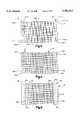
- FIG. 3is a bottom plan view of the face of the chip cube having the chip contacts thereon;
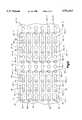
- FIG. 4is an X-ray top plan view of the cube mounting face of an interposer for use in connecting IC chips;
- FIG. 5is a bottom plan view of the output face of the interposer of FIG. 4;
- FIG. 6is a top plan view of a portion of the cube mounting face of the interposer showing customized electrical connections
- FIG. 7is an X-ray bottom plan view of a portion of the interposer showing custom circuitization
- FIG. 8is a sectional view taken through a portion of an interposer and portions of the chip stack showing a technique of chip shifting to provide connection;
- FIG. 9is a longitudinal sectional view of a portion of another embodiment of an interposer.
- the chip cubeis formed of a plurality of integrated circuit chips 10, each of which is formed with a conventional footprint comprised of a plurality of input/output (I/O) connections 12 thereon.
- I/O connections 12have circuit lines 14 leading therefrom to one edge of the chip 10.
- the chips 10are secured together in front-to-back relationship by means of thin films of adhesive 18 which form the chips generally into a stack or cube.
- the chips 10-1 through 10-nare arranged so that the circuitry 14 terminates at a connector surface 22 on the cube 20, at which the circuitry 14 terminates and forms an array of connections 24 thereon.
- the connectionsare designated as 24a, 24b. . . 24m (in this case, "m" designates an end number in a series).
- a given connection or a particular chipwould be designated, e.g., connection 24a-1, or 24b-3, etc.
- the chips 10-1 to 10-nare tested prior to formation into the cube 20, but the chips are not burned in until after they are formed into the cube 20.
- one or more of the chipsmay fail; i.e., one or more of the connections 24a-24m on any one chip 10 may fail to perform during testing. If the cube were arranged to include just enough chips to satisfy the connection requirements to a substrate, as will be explained presently, and one of the chips failed or indeed one connection 24 on one chip 10 failed, the entire cube would be inoperative and would have to be scrapped since typically every connection is required to operate. Therefore, it is common practice to provide more chips in the cube than are necessary to form the connections.
- each of the chipsis substantially identical in construction, and the chips are completely interchangeable, one with the other; i.e., any twenty chips can be used, and any one chip can substitute for any other chip.
- an interposer 26is provided which is formed of a dielectric material such as composite reinforced polytetrafluoroethylene (PTFE) or polyimide. As shown in FIGS. 2, 4 and 5, the interposer has a cube mounting surface 28 and an output surface 30.
- the cube mounting surface 28has an array of chip attachment pads 32 thereon, which correspond in number and location to the connector pads 24 on the face 22 of the cube 20.
- the interposer 26there is provided on the cube mounting surface 28 of the interposer 26 a number of pads which are located so that all of the connectors 24a-24m on all of the chips 10-1 through 10-n can be connected to the chip attachment pads 32; i.e., the pads 24a-24m of each of the twenty-four chips 10-1 through 10-24 has a corresponding attachment pad 32a-32m on the surface 28 of the interposer 26.
- the output surface 30 of the interposer 26is provided with a series of output pads 34a-34m, which correspond in location and number to the number of connections which need to be made; i.e., if twenty chips are to be functional, there will be twenty sets of pads 34a-34m. As indicated above, these pads 34a-34m will correspond in location and number to the number of connections required for the I/Os of the cube in its functional environment. It then becomes necessary to identify the functioning chips in the cube. There must be enough functioning chips in the cube to meet the requirements of all of the I/O pads 34a-34m. In the example used, there must be twenty functioning chips, or expressed another way, there can be no more than 4 non-functioning chips.
- thiscan be expressed as a chip array or cube having X+Y number of chips wherein X and Y are positive integers and wherein there must be at least X number of functioning chips (i.e., a chip where all connections 24a-24m of the chip work). Thus, as indicated in the example chosen, there must be at least twenty functioning chips, and hence, no more than four non-functioning chips.
- the interposeris then wired to connect a selected twenty functioning chips to the twenty rows of chip output pads 34a-34m on the output surface 30. This is done by means of wiring the chip attachments pads 32a-32m to the output pads 34a-34m through vias 36 formed in the interposer, each of the vias extending from the chip mounting surface 28 to the output surface 30.
- These vias 36are preferably in the form of plated through holes, and thus surface wiring on either the output surface 30 or the cube mounting surface 28, or both, can be used to attach the connection 24a-24m of each of the functioning chips to the output pads 34a-34m.
- FIGS. 6 and 7One technique for wiring the chips is shown in FIGS. 6 and 7.
- the top and bottom surfaces of the interposer 20are used as wiring channels to selectively wire the selected functioning chips to the output pads 34a-34m on the bottom surface of the interposer.
- 6 and 7are somewhat schematic and show somewhat diagrammatically the technique of wiring just a few chips of the array, it being understood that this technique applies to all of the chips and all connection sites on each chip.)
- the chip which is bonded to the pads 32a-1 through 32m-1 to outlet pads 34a-4 to 34m-4and to wire the chip attached to the pads 32a-8 through 32m-8 to outlet pads 34a-5 to 34m-5;
- the chips attached to 32a-2 to 32m-2are wired to pads 34a-2 to 34m-2;
- the chips connected to pads 32a-3 to 32m-3are wired to pads 34a-3 to 34m-3;
- the chips wired to 32a-6 through 32m-6are wired to pads 34a-6 to 34m-6; and chips attached to pads 32a-7 through 32m-7 are wired to pads 34a-7 to 34m-7.
- each of the pads 32a-1 to 32m-1, 32a-2 to 32m-2, 32a-3 to 32m-3, 32a-6 to 32m-6 and 32a-7 to 32m-7are connected by circuit traces 38 to their next adjacent via 36 as seen in FIG. 6.
- the pads 34a-2 to 34m-2, 34a-3 to 34m-3, 34a-4 to 34m-4, 34a-5 to 34m-5, 34a-6 to 34m-6, and 34a-7 to 34m-7are also connected to their next adjacent vias 36 by circuit traces 39 on the bottom.
- the pads 32a-1 through 32m-1are connected to their adjacent vias 36, which in turn are connected to vias 36 by surface wiring 40 on surface 28, and which vias 36 on the bottom surface 30 are connected to pads 34a-4 through 34m-4 by traces 39.
- thiseffectively connects the chip that is connected to the pads 32a-1 through 32m-1 around some pads to the pads 34a-4 through 34m-4 for output.
- the chip connected to pads 32a-8 through 32m-8is connected through via 36 adjacent thereto to the vias on the bottom adjacent to pads 34a-5 through 34m-5 by surface wiring 41 on surface 30, thus effectively connecting the chips that are connected to the pads 32a-8 through 32m-8 to the pads 34a-5 through 34m-5.
- the chip footprint connected on the bottomrepresents pads 34a-2 through 34m-2, 34a-3 through 34m-3, 34a-4 through 34m-4, 34a-5 through 34m-5, 34a-6 through 34m-6 and 34a-7 through 34m-7. These are the pads then that are soldered by solder ball connection 44 (see FIG. 8) or otherwise joined to a substrate to form the connection to the chips, which chips are soldered or otherwise connected to the pads 32.
- FIG. 8is a sectional view through connections 32a-1, 32a-2, 32a-3, 32a-4, 32a-5, 32a-6 and 32a-7 and pads 34a-1, 34a-2, 34a-3, 34a-4, 34a-5, 34a-6 and 34a-7 in connecting a chip stack 20 to a substrate utilizing a technique known as chip shifting. Wiring in the channel is not required in this technique. This also depicts the connection of the chip cube 20 to the pads 32 by means of solder balls 42 and the connection of the pads 34 by solder balls 44 to pads 46 on a substrate 48.
- pad 32a-1is connected through via 36a-1 to pad 34a-2; pad 32a-2 is connected through via 36a-2 to pad 34a-3; pad 32a-3 is not connected to any pad; pad 32a-4 is connected through via 36a-4 to pad 34a-4; pad 32a-5 is connected through via 36a-5 to pad 34a-5; pad 32a-6 is not connected to any pad; and pad 32a-7 is connected through via 36a-6 to pad 34a-6.
- chip shiftingwherein a chip can be connected to a pad directly beneath or within one of the pads.
- the connection of the chipscan be shifted one position either left or right without the need to use any channels on the surface of the interposer for wiring.
- Chip shiftingcan be used instead of or in combination with the surface wiring as shown in FIGS. 6 and 7.
- the interposercan be custom-wired to connect with those functioning chips, wherever they are located in the stack, and provide the necessary footprint on the output.
- the interposercould be partially formed and maintained in stock, i.e., the pads 32 and 34 on both sides and the vias 36 formed in the interposer without connections using standard photolithographic and metalization processing. Once the pattern of functioning chips has been determined, the necessary connections can be formed, again using standard photolithographic techniques.
- the interposercan be formed starting with the dielectric material as a blank and forming all of the pads, vias and interconnections after the determination has been made as to which chips are to be functional and which chips are non-functional chips. In this way, the entire stack of chips need not be scrapped due to the lack of functioning of a single connection.
- a standard footprintcan be used, and only a single part or a very limited number of parts need be stored through the interposer, with the customization being done quickly and rapidly once the determination has been made as to which chips are functional in the stack.
- interposercan be formed with all of the holes drilled, and plated with copper, and all circuit-receiving surfaces blanket plated with copper. After the determination of which chips are to be used as good chips, the required pads and interconnections are defined by subtractive etching. Both additive and subtractive circuitization as described require custom art work.
- Another technology that can be usedis laser direct write lithography to customize the part by either additive or substractive processes.
- FIG. 9a longitudinal sectional view of a portion of another embodiment of an interposer according to this invention is shown.
- This embodimentis particularly useful to accommodate differences in the coefficient of thermal expansion (CTE) of components.
- CTEcoefficient of thermal expansion
- the interposer designated by the reference character 80is comprised of a sheet of metal 82 laminated between a pair of silica filled polytetrafluoroethylene (PTFE) sheets 84, 86. Holes 88 are pre-formed in the plate 82 where vias 90 are to be formed.
- PTFEpolytetrafluoroethylene
- the lamination of the sheets 84 and 86 under heat and pressurecauses the PTFE material therefrom to fill the holes 88 during lamination.
- the vias 90are then formed, and the interposer circuitized, including top surface metallurgy 32, bottom surface metallurgy 34, and plated through holes 36 are formed in a conventional manner.
- the metal sheet 82is selected such that it, together with the PTFE material, provides a composite CTE of the desired value.
- the metalcould be copper, or invar or copper-clad invar (CIC).
- the composite CTE of the interposer 80is selected to be about 10 ppm/°C. for a chip stack, although other values could be selected depending upon well-known design considerations.
Landscapes
- Engineering & Computer Science (AREA)
- Microelectronics & Electronic Packaging (AREA)
- Power Engineering (AREA)
- Physics & Mathematics (AREA)
- Condensed Matter Physics & Semiconductors (AREA)
- General Physics & Mathematics (AREA)
- Computer Hardware Design (AREA)
- Manufacturing & Machinery (AREA)
- Semiconductor Integrated Circuits (AREA)
- Tests Of Electronic Circuits (AREA)
Abstract
Description
Claims (8)
Priority Applications (2)
| Application Number | Priority Date | Filing Date | Title |
|---|---|---|---|
| US08/719,826US5781413A (en) | 1996-09-30 | 1996-09-30 | Method and apparatus for directing the input/output connection of integrated circuit chip cube configurations |
| KR1019970022763AKR100256471B1 (en) | 1996-09-30 | 1997-06-02 | Method and apparatus for directing the input/output connection of integrated circuit chip cube configurations |
Applications Claiming Priority (1)
| Application Number | Priority Date | Filing Date | Title |
|---|---|---|---|
| US08/719,826US5781413A (en) | 1996-09-30 | 1996-09-30 | Method and apparatus for directing the input/output connection of integrated circuit chip cube configurations |
Publications (1)
| Publication Number | Publication Date |
|---|---|
| US5781413Atrue US5781413A (en) | 1998-07-14 |
Family
ID=24891508
Family Applications (1)
| Application Number | Title | Priority Date | Filing Date |
|---|---|---|---|
| US08/719,826Expired - LifetimeUS5781413A (en) | 1996-09-30 | 1996-09-30 | Method and apparatus for directing the input/output connection of integrated circuit chip cube configurations |
Country Status (2)
| Country | Link |
|---|---|
| US (1) | US5781413A (en) |
| KR (1) | KR100256471B1 (en) |
Cited By (12)
| Publication number | Priority date | Publication date | Assignee | Title |
|---|---|---|---|---|
| US6008530A (en)* | 1997-05-29 | 1999-12-28 | Nec Corporation | Polyhedral IC package for making three dimensionally expandable assemblies |
| US6075284A (en)* | 1998-06-30 | 2000-06-13 | Hyundai Electronics Industries Co., Ltd. | Stack package |
| US6137162A (en)* | 1998-05-12 | 2000-10-24 | Hyundai Electronics Industries Co., Ltd. | Chip stack package |
| US6316825B1 (en) | 1998-05-15 | 2001-11-13 | Hyundai Electronics Industries Co., Ltd. | Chip stack package utilizing a connecting hole to improve electrical connection between leadframes |
| US6486415B2 (en) | 2001-01-16 | 2002-11-26 | International Business Machines Corporation | Compliant layer for encapsulated columns |
| US20030049424A1 (en)* | 2001-09-07 | 2003-03-13 | Yamaguchi James Satsuo | Stacking of multilayer modules |
| WO2003023823A3 (en)* | 2001-09-07 | 2003-12-11 | Irvine Sensors Corp | Stacking of multilayer modules |
| US6709964B2 (en) | 1999-07-21 | 2004-03-23 | Samsung Electronics Co., Ltd. | Semiconductor device and manufacturing method using a stress-relieving film attached to solder joints |
| US6774315B1 (en) | 2000-05-24 | 2004-08-10 | International Business Machines Corporation | Floating interposer |
| US8299592B2 (en) | 2009-01-23 | 2012-10-30 | Hynix Semiconductor Inc. | Cube semiconductor package composed of a plurality of stacked together and interconnected semiconductor chip modules |
| US20130025927A1 (en)* | 2011-07-25 | 2013-01-31 | International Business Machines Corporation | Modified 0402 Footprint For A Printed Circuit Board ('PCB') |
| US8933715B2 (en) | 2012-04-08 | 2015-01-13 | Elm Technology Corporation | Configurable vertical integration |
Families Citing this family (1)
| Publication number | Priority date | Publication date | Assignee | Title |
|---|---|---|---|---|
| KR101215975B1 (en) | 2011-02-28 | 2012-12-27 | 에스케이하이닉스 주식회사 | Semiconductor device and fabrication method of the same |
Citations (21)
| Publication number | Priority date | Publication date | Assignee | Title |
|---|---|---|---|---|
| US4574331A (en)* | 1983-05-31 | 1986-03-04 | Trw Inc. | Multi-element circuit construction |
| US4727410A (en)* | 1983-11-23 | 1988-02-23 | Cabot Technical Ceramics, Inc. | High density integrated circuit package |
| US4813129A (en)* | 1987-06-19 | 1989-03-21 | Hewlett-Packard Company | Interconnect structure for PC boards and integrated circuits |
| US5007841A (en)* | 1983-05-31 | 1991-04-16 | Trw Inc. | Integrated-circuit chip interconnection system |
| US5016138A (en)* | 1987-10-27 | 1991-05-14 | Woodman John K | Three dimensional integrated circuit package |
| US5051865A (en)* | 1985-06-17 | 1991-09-24 | Fujitsu Limited | Multi-layer semiconductor device |
| US5177594A (en)* | 1991-01-09 | 1993-01-05 | International Business Machines Corporation | Semiconductor chip interposer module with engineering change wiring and distributed decoupling capacitance |
| US5224918A (en)* | 1991-06-27 | 1993-07-06 | Cray Research, Inc. | Method of manufacturing metal connector blocks |
| US5252857A (en)* | 1991-08-05 | 1993-10-12 | International Business Machines Corporation | Stacked DCA memory chips |
| US5281852A (en)* | 1991-12-10 | 1994-01-25 | Normington Peter J C | Semiconductor device including stacked die |
| US5311401A (en)* | 1991-07-09 | 1994-05-10 | Hughes Aircraft Company | Stacked chip assembly and manufacturing method therefor |
| US5327327A (en)* | 1992-10-30 | 1994-07-05 | Texas Instruments Incorporated | Three dimensional assembly of integrated circuit chips |
| US5343075A (en)* | 1991-06-29 | 1994-08-30 | Sony Corporation | Composite stacked semiconductor device with contact plates |
| US5406565A (en)* | 1989-06-07 | 1995-04-11 | Mv Limited | Memory array of integrated circuits capable of replacing faulty cells with a spare |
| US5414637A (en)* | 1992-06-24 | 1995-05-09 | International Business Machines Corporation | Intra-module spare routing for high density electronic packages |
| US5432729A (en)* | 1993-04-23 | 1995-07-11 | Irvine Sensors Corporation | Electronic module comprising a stack of IC chips each interacting with an IC chip secured to the stack |
| US5434745A (en)* | 1994-07-26 | 1995-07-18 | White Microelectronics Div. Of Bowmar Instrument Corp. | Stacked silicon die carrier assembly |
| US5502333A (en)* | 1994-03-30 | 1996-03-26 | International Business Machines Corporation | Semiconductor stack structures and fabrication/sparing methods utilizing programmable spare circuit |
| US5561593A (en)* | 1994-01-27 | 1996-10-01 | Vicon Enterprises, Inc. | Z-interface-board |
| US5686843A (en)* | 1995-06-30 | 1997-11-11 | International Business Machines Corporation | Methods and apparatus for burn-in stressing and simultaneous testing of semiconductor device chips in a multichip module |
| US5691041A (en)* | 1995-09-29 | 1997-11-25 | International Business Machines Corporation | Socket for semi-permanently connecting a solder ball grid array device using a dendrite interposer |
- 1996
- 1996-09-30USUS08/719,826patent/US5781413A/ennot_activeExpired - Lifetime
- 1997
- 1997-06-02KRKR1019970022763Apatent/KR100256471B1/ennot_activeExpired - Fee Related
Patent Citations (21)
| Publication number | Priority date | Publication date | Assignee | Title |
|---|---|---|---|---|
| US4574331A (en)* | 1983-05-31 | 1986-03-04 | Trw Inc. | Multi-element circuit construction |
| US5007841A (en)* | 1983-05-31 | 1991-04-16 | Trw Inc. | Integrated-circuit chip interconnection system |
| US4727410A (en)* | 1983-11-23 | 1988-02-23 | Cabot Technical Ceramics, Inc. | High density integrated circuit package |
| US5051865A (en)* | 1985-06-17 | 1991-09-24 | Fujitsu Limited | Multi-layer semiconductor device |
| US4813129A (en)* | 1987-06-19 | 1989-03-21 | Hewlett-Packard Company | Interconnect structure for PC boards and integrated circuits |
| US5016138A (en)* | 1987-10-27 | 1991-05-14 | Woodman John K | Three dimensional integrated circuit package |
| US5406565A (en)* | 1989-06-07 | 1995-04-11 | Mv Limited | Memory array of integrated circuits capable of replacing faulty cells with a spare |
| US5177594A (en)* | 1991-01-09 | 1993-01-05 | International Business Machines Corporation | Semiconductor chip interposer module with engineering change wiring and distributed decoupling capacitance |
| US5224918A (en)* | 1991-06-27 | 1993-07-06 | Cray Research, Inc. | Method of manufacturing metal connector blocks |
| US5343075A (en)* | 1991-06-29 | 1994-08-30 | Sony Corporation | Composite stacked semiconductor device with contact plates |
| US5311401A (en)* | 1991-07-09 | 1994-05-10 | Hughes Aircraft Company | Stacked chip assembly and manufacturing method therefor |
| US5252857A (en)* | 1991-08-05 | 1993-10-12 | International Business Machines Corporation | Stacked DCA memory chips |
| US5281852A (en)* | 1991-12-10 | 1994-01-25 | Normington Peter J C | Semiconductor device including stacked die |
| US5414637A (en)* | 1992-06-24 | 1995-05-09 | International Business Machines Corporation | Intra-module spare routing for high density electronic packages |
| US5327327A (en)* | 1992-10-30 | 1994-07-05 | Texas Instruments Incorporated | Three dimensional assembly of integrated circuit chips |
| US5432729A (en)* | 1993-04-23 | 1995-07-11 | Irvine Sensors Corporation | Electronic module comprising a stack of IC chips each interacting with an IC chip secured to the stack |
| US5561593A (en)* | 1994-01-27 | 1996-10-01 | Vicon Enterprises, Inc. | Z-interface-board |
| US5502333A (en)* | 1994-03-30 | 1996-03-26 | International Business Machines Corporation | Semiconductor stack structures and fabrication/sparing methods utilizing programmable spare circuit |
| US5434745A (en)* | 1994-07-26 | 1995-07-18 | White Microelectronics Div. Of Bowmar Instrument Corp. | Stacked silicon die carrier assembly |
| US5686843A (en)* | 1995-06-30 | 1997-11-11 | International Business Machines Corporation | Methods and apparatus for burn-in stressing and simultaneous testing of semiconductor device chips in a multichip module |
| US5691041A (en)* | 1995-09-29 | 1997-11-25 | International Business Machines Corporation | Socket for semi-permanently connecting a solder ball grid array device using a dendrite interposer |
Non-Patent Citations (2)
| Title |
|---|
| "Silicon Cube Burn-In Methodology," K.E. Beilstein, et al., IBM Technical Disclosure Bulletin, vol. 37, No. 07, Jul., 1994. |
| Silicon Cube Burn In Methodology, K.E. Beilstein, et al., IBM Technical Disclosure Bulletin, vol. 37, No. 07, Jul., 1994.* |
Cited By (22)
| Publication number | Priority date | Publication date | Assignee | Title |
|---|---|---|---|---|
| US6008530A (en)* | 1997-05-29 | 1999-12-28 | Nec Corporation | Polyhedral IC package for making three dimensionally expandable assemblies |
| US6137162A (en)* | 1998-05-12 | 2000-10-24 | Hyundai Electronics Industries Co., Ltd. | Chip stack package |
| US6316825B1 (en) | 1998-05-15 | 2001-11-13 | Hyundai Electronics Industries Co., Ltd. | Chip stack package utilizing a connecting hole to improve electrical connection between leadframes |
| US6075284A (en)* | 1998-06-30 | 2000-06-13 | Hyundai Electronics Industries Co., Ltd. | Stack package |
| US6709964B2 (en) | 1999-07-21 | 2004-03-23 | Samsung Electronics Co., Ltd. | Semiconductor device and manufacturing method using a stress-relieving film attached to solder joints |
| US6946329B2 (en) | 2000-05-24 | 2005-09-20 | International Business Machines Corporation | Methods of making and using a floating interposer |
| US6774315B1 (en) | 2000-05-24 | 2004-08-10 | International Business Machines Corporation | Floating interposer |
| US20030020150A1 (en)* | 2001-01-16 | 2003-01-30 | International Business Machines Corporation | Compliant layer for encapsulated columns |
| US7278207B2 (en) | 2001-01-16 | 2007-10-09 | International Business Machines Corporation | Method of making an electronic package |
| US20070278654A1 (en)* | 2001-01-16 | 2007-12-06 | Jimarez Lisa J | Method of making an electronic package |
| US20050250249A1 (en)* | 2001-01-16 | 2005-11-10 | Jimarez Lisa J | Method of making an electronic package |
| US6486415B2 (en) | 2001-01-16 | 2002-11-26 | International Business Machines Corporation | Compliant layer for encapsulated columns |
| US6961995B2 (en) | 2001-01-16 | 2005-11-08 | International Business Machines Corporation | Method of making an electronic package |
| US20030049424A1 (en)* | 2001-09-07 | 2003-03-13 | Yamaguchi James Satsuo | Stacking of multilayer modules |
| WO2003023823A3 (en)* | 2001-09-07 | 2003-12-11 | Irvine Sensors Corp | Stacking of multilayer modules |
| US6717061B2 (en) | 2001-09-07 | 2004-04-06 | Irvine Sensors Corporation | Stacking of multilayer modules |
| US8299592B2 (en) | 2009-01-23 | 2012-10-30 | Hynix Semiconductor Inc. | Cube semiconductor package composed of a plurality of stacked together and interconnected semiconductor chip modules |
| US20130025927A1 (en)* | 2011-07-25 | 2013-01-31 | International Business Machines Corporation | Modified 0402 Footprint For A Printed Circuit Board ('PCB') |
| US8664541B2 (en)* | 2011-07-25 | 2014-03-04 | International Business Machines Corporation | Modified 0402 footprint for a printed circuit board (‘PCB’) |
| US8933715B2 (en) | 2012-04-08 | 2015-01-13 | Elm Technology Corporation | Configurable vertical integration |
| US9726716B2 (en) | 2013-03-13 | 2017-08-08 | Glenn J Leedy | Configurable vertical integration |
| US9804221B2 (en) | 2013-03-13 | 2017-10-31 | Glenn J Leedy | Configurable vertical integration |
Also Published As
| Publication number | Publication date |
|---|---|
| KR19980024039A (en) | 1998-07-06 |
| KR100256471B1 (en) | 2000-05-15 |
Similar Documents
| Publication | Publication Date | Title |
|---|---|---|
| US5815374A (en) | Method and apparatus for redirecting certain input/output connections of integrated circuit chip configurations | |
| EP0460822B1 (en) | Integrated circuit packaging using flexible substrate | |
| US5576519A (en) | Anisotropic interconnect methodology for cost effective manufacture of high density printed wiring boards | |
| US5375042A (en) | Semiconductor package employing substrate assembly having a pair of thin film circuits disposed one on each of oppositely facing surfaces of a thick film circuit | |
| US5432677A (en) | Multi-chip integrated circuit module | |
| US4648179A (en) | Process of making interconnection structure for semiconductor device | |
| US6205654B1 (en) | Method of manufacturing a surface mount package | |
| US5386627A (en) | Method of fabricating a multi-layer integrated circuit chip interposer | |
| US7288433B2 (en) | Method of making assemblies having stacked semiconductor chips | |
| US6400573B1 (en) | Multi-chip integrated circuit module | |
| US5781413A (en) | Method and apparatus for directing the input/output connection of integrated circuit chip cube configurations | |
| US4755866A (en) | Electronic circuit module | |
| US6759270B2 (en) | Semiconductor chip module and method of manufacture of same | |
| US3952231A (en) | Functional package for complex electronic systems with polymer-metal laminates and thermal transposer | |
| US4970106A (en) | Thin film multilayer laminate interconnection board | |
| JPH04233256A (en) | Electronic device | |
| US20090178273A1 (en) | Method of making circuitized assembly including a plurality of circuitized substrates | |
| JPH10284632A (en) | Circuit board and method of manufacturing the same | |
| US6537852B2 (en) | Spacer - connector stud for stacked surface laminated multichip modules and methods of manufacture | |
| JPH0476505B2 (en) | ||
| EP0521720A1 (en) | Heat-dissipating multi-layer circuit board | |
| JPS61148706A (en) | Flexible cable assembly | |
| US6657295B2 (en) | Multilayer interconnect board and multilayer semiconductor device | |
| US7180752B2 (en) | Method and structures for implementing enhanced reliability for printed circuit board high power dissipation applications | |
| JPH03142943A (en) | Combination of semiconductor device and printed wiring board structure |
Legal Events
| Date | Code | Title | Description |
|---|---|---|---|
| AS | Assignment | Owner name:INTERNATIONAL BUSINESS MACHINES CORPORATION, A COR Free format text:ASSIGNMENT OF ASSIGNORS INTEREST;ASSIGNORS:HOWELL, WAYNE JOHN;KRESGE, JOHN STEVEN;STONE, DAVID BRIAN;AND OTHERS;REEL/FRAME:008195/0381;SIGNING DATES FROM 19960906 TO 19960924 | |
| STCF | Information on status: patent grant | Free format text:PATENTED CASE | |
| FPAY | Fee payment | Year of fee payment:4 | |
| FPAY | Fee payment | Year of fee payment:8 | |
| FPAY | Fee payment | Year of fee payment:12 | |
| AS | Assignment | Owner name:GLOBALFOUNDRIES U.S. 2 LLC, NEW YORK Free format text:ASSIGNMENT OF ASSIGNORS INTEREST;ASSIGNOR:INTERNATIONAL BUSINESS MACHINES CORPORATION;REEL/FRAME:036550/0001 Effective date:20150629 | |
| AS | Assignment | Owner name:GLOBALFOUNDRIES INC., CAYMAN ISLANDS Free format text:ASSIGNMENT OF ASSIGNORS INTEREST;ASSIGNORS:GLOBALFOUNDRIES U.S. 2 LLC;GLOBALFOUNDRIES U.S. INC.;REEL/FRAME:036779/0001 Effective date:20150910 | |
| AS | Assignment | Owner name:GLOBALFOUNDRIES U.S. INC., NEW YORK Free format text:RELEASE BY SECURED PARTY;ASSIGNOR:WILMINGTON TRUST, NATIONAL ASSOCIATION;REEL/FRAME:056987/0001 Effective date:20201117 |