US5781331A - Optical microshutter array - Google Patents
Optical microshutter arrayDownload PDFInfo
- Publication number
- US5781331A US5781331AUS08/787,307US78730797AUS5781331AUS 5781331 AUS5781331 AUS 5781331AUS 78730797 AUS78730797 AUS 78730797AUS 5781331 AUS5781331 AUS 5781331A
- Authority
- US
- United States
- Prior art keywords
- aperture
- recited
- aperture plate
- layer
- illumination
- Prior art date
- Legal status (The legal status is an assumption and is not a legal conclusion. Google has not performed a legal analysis and makes no representation as to the accuracy of the status listed.)
- Expired - Fee Related
Links
- 230000003287optical effectEffects0.000titleclaimsabstractdescription41
- 238000005286illuminationMethods0.000claimsabstractdescription24
- 238000010438heat treatmentMethods0.000claimsabstractdescription9
- 230000001747exhibiting effectEffects0.000claimsabstractdescription6
- 230000005540biological transmissionEffects0.000claimsabstractdescription4
- XUIMIQQOPSSXEZ-UHFFFAOYSA-NSiliconChemical compound[Si]XUIMIQQOPSSXEZ-UHFFFAOYSA-N0.000claimsdescription24
- 229910052710siliconInorganic materials0.000claimsdescription23
- 239000010703siliconSubstances0.000claimsdescription23
- 108091008695photoreceptorsProteins0.000claimsdescription5
- 230000033001locomotionEffects0.000claimsdescription3
- 238000001514detection methodMethods0.000claims6
- 229910021420polycrystalline siliconInorganic materials0.000description16
- 229920005591polysiliconPolymers0.000description16
- 239000000758substrateSubstances0.000description16
- 229910052581Si3N4Inorganic materials0.000description7
- HQVNEWCFYHHQES-UHFFFAOYSA-Nsilicon nitrideChemical compoundN12[Si]34N5[Si]62N3[Si]51N64HQVNEWCFYHHQES-UHFFFAOYSA-N0.000description7
- 238000004519manufacturing processMethods0.000description6
- 239000010408filmSubstances0.000description5
- 238000000034methodMethods0.000description4
- 238000003491arrayMethods0.000description3
- 230000001427coherent effectEffects0.000description3
- 238000005459micromachiningMethods0.000description3
- 230000005855radiationEffects0.000description3
- 239000004065semiconductorSubstances0.000description3
- 239000010409thin filmSubstances0.000description3
- 229910052782aluminiumInorganic materials0.000description2
- XAGFODPZIPBFFR-UHFFFAOYSA-NaluminiumChemical compound[Al]XAGFODPZIPBFFR-UHFFFAOYSA-N0.000description2
- 230000008021depositionEffects0.000description2
- 238000001914filtrationMethods0.000description2
- PCHJSUWPFVWCPO-UHFFFAOYSA-NgoldChemical compound[Au]PCHJSUWPFVWCPO-UHFFFAOYSA-N0.000description2
- 229910052737goldInorganic materials0.000description2
- 239000010931goldSubstances0.000description2
- 229910052751metalInorganic materials0.000description2
- 239000002184metalSubstances0.000description2
- 238000012986modificationMethods0.000description2
- 230000004048modificationEffects0.000description2
- VYZAMTAEIAYCRO-UHFFFAOYSA-NChromiumChemical compound[Cr]VYZAMTAEIAYCRO-UHFFFAOYSA-N0.000description1
- 239000000654additiveSubstances0.000description1
- 230000000996additive effectEffects0.000description1
- 238000005452bendingMethods0.000description1
- 229910052804chromiumInorganic materials0.000description1
- 239000011651chromiumSubstances0.000description1
- 239000004020conductorSubstances0.000description1
- 238000001816coolingMethods0.000description1
- 230000001419dependent effectEffects0.000description1
- 238000013461designMethods0.000description1
- 238000011161developmentMethods0.000description1
- 238000006073displacement reactionMethods0.000description1
- 230000000694effectsEffects0.000description1
- 238000005421electrostatic potentialMethods0.000description1
- 238000005530etchingMethods0.000description1
- 230000002452interceptive effectEffects0.000description1
- 239000000463materialSubstances0.000description1
- 230000037361pathwayEffects0.000description1
- 238000012545processingMethods0.000description1
- 238000004445quantitative analysisMethods0.000description1
- 230000035945sensitivityEffects0.000description1
- 239000007787solidSubstances0.000description1
- 230000000153supplemental effectEffects0.000description1
- 238000012360testing methodMethods0.000description1
Images


Classifications
- G—PHYSICS
- G01—MEASURING; TESTING
- G01J—MEASUREMENT OF INTENSITY, VELOCITY, SPECTRAL CONTENT, POLARISATION, PHASE OR PULSE CHARACTERISTICS OF INFRARED, VISIBLE OR ULTRAVIOLET LIGHT; COLORIMETRY; RADIATION PYROMETRY
- G01J3/00—Spectrometry; Spectrophotometry; Monochromators; Measuring colours
- G01J3/02—Details
- G01J3/10—Arrangements of light sources specially adapted for spectrometry or colorimetry
- G—PHYSICS
- G01—MEASURING; TESTING
- G01J—MEASUREMENT OF INTENSITY, VELOCITY, SPECTRAL CONTENT, POLARISATION, PHASE OR PULSE CHARACTERISTICS OF INFRARED, VISIBLE OR ULTRAVIOLET LIGHT; COLORIMETRY; RADIATION PYROMETRY
- G01J3/00—Spectrometry; Spectrophotometry; Monochromators; Measuring colours
- G01J3/02—Details
- G01J3/0205—Optical elements not provided otherwise, e.g. optical manifolds, diffusers, windows
- G01J3/0232—Optical elements not provided otherwise, e.g. optical manifolds, diffusers, windows using shutters
- G—PHYSICS
- G02—OPTICS
- G02B—OPTICAL ELEMENTS, SYSTEMS OR APPARATUS
- G02B26/00—Optical devices or arrangements for the control of light using movable or deformable optical elements
- G02B26/02—Optical devices or arrangements for the control of light using movable or deformable optical elements for controlling the intensity of light
- G—PHYSICS
- G02—OPTICS
- G02B—OPTICAL ELEMENTS, SYSTEMS OR APPARATUS
- G02B6/00—Light guides; Structural details of arrangements comprising light guides and other optical elements, e.g. couplings
- G02B6/24—Coupling light guides
- G02B6/26—Optical coupling means
- G02B6/35—Optical coupling means having switching means
- G02B6/351—Optical coupling means having switching means involving stationary waveguides with moving interposed optical elements
- G02B6/353—Optical coupling means having switching means involving stationary waveguides with moving interposed optical elements the optical element being a shutter, baffle, beam dump or opaque element
- G—PHYSICS
- G02—OPTICS
- G02B—OPTICAL ELEMENTS, SYSTEMS OR APPARATUS
- G02B6/00—Light guides; Structural details of arrangements comprising light guides and other optical elements, e.g. couplings
- G02B6/24—Coupling light guides
- G02B6/26—Optical coupling means
- G02B6/35—Optical coupling means having switching means
- G02B6/354—Switching arrangements, i.e. number of input/output ports and interconnection types
- G02B6/3544—2D constellations, i.e. with switching elements and switched beams located in a plane
- G02B6/3548—1xN switch, i.e. one input and a selectable single output of N possible outputs
- G02B6/3552—1x1 switch, e.g. on/off switch
- G—PHYSICS
- G02—OPTICS
- G02B—OPTICAL ELEMENTS, SYSTEMS OR APPARATUS
- G02B6/00—Light guides; Structural details of arrangements comprising light guides and other optical elements, e.g. couplings
- G02B6/24—Coupling light guides
- G02B6/26—Optical coupling means
- G02B6/35—Optical coupling means having switching means
- G02B6/3564—Mechanical details of the actuation mechanism associated with the moving element or mounting mechanism details
- G02B6/3566—Mechanical details of the actuation mechanism associated with the moving element or mounting mechanism details involving bending a beam, e.g. with cantilever
- G—PHYSICS
- G02—OPTICS
- G02B—OPTICAL ELEMENTS, SYSTEMS OR APPARATUS
- G02B6/00—Light guides; Structural details of arrangements comprising light guides and other optical elements, e.g. couplings
- G02B6/24—Coupling light guides
- G02B6/26—Optical coupling means
- G02B6/35—Optical coupling means having switching means
- G02B6/3564—Mechanical details of the actuation mechanism associated with the moving element or mounting mechanism details
- G02B6/3568—Mechanical details of the actuation mechanism associated with the moving element or mounting mechanism details characterised by the actuating force
- G02B6/3578—Piezoelectric force
- G—PHYSICS
- G02—OPTICS
- G02B—OPTICAL ELEMENTS, SYSTEMS OR APPARATUS
- G02B6/00—Light guides; Structural details of arrangements comprising light guides and other optical elements, e.g. couplings
- G02B6/24—Coupling light guides
- G02B6/26—Optical coupling means
- G02B6/35—Optical coupling means having switching means
- G02B6/3564—Mechanical details of the actuation mechanism associated with the moving element or mounting mechanism details
- G02B6/3584—Mechanical details of the actuation mechanism associated with the moving element or mounting mechanism details constructional details of an associated actuator having a MEMS construction, i.e. constructed using semiconductor technology such as etching
Definitions
- This inventionrelates to microstructures that are constructed utilizing semiconductor fabrication processes and, more particularly, to an optical microshutter array produced in accordance with such semiconductor fabrication processes.
- Silicon "micromachining”has been developed as a means for accurately fabricating small structures. Such processing involves the selective etching of a silicon substrate and the deposition thereon of thin film layers of semiconductor materials. Various sacrificial layers are employed to enable the fabrication of relatively complex interactive structures.
- Silicon micromachininghas been applied to the fabrication of micromachines that include rotary and linear bearings. Such bearings have spawned further development of electrically-driven motors which exhibit a planar geometry and lateral dimensions on the order of 100 microns or so. In addition to micromotors, various cantilever structures have also been constructed utilizing micromachining concepts.
- FIGS. 1a and 1billustrate a prior art cantilever device wherein a polysilicon layer 10 is bonded to a layer 12 of different composition. Both layers are attached, at one extremity, to a substrate 14.
- the thermal coefficients of expansion of polysilicon layer 10 and layer 12are chosen as to be sufficiently different that, without an applied potential to create a heating action, the structure exhibits an arcuate form as shown in FIG. 1a.
- a voltage Vtis applied to a resistive portion of polysilicon layer 10
- current flowcauses a heating of both layers and unequal expansion results in a clockwise rotation of the arm until contact is made with substrate contact region 16.
- FIGS. 1a and 1bThe action of the cantilever structure of FIGS. 1a and 1b is much the same as a well known bi-metal thermal actuator widely used in thermostats. Further details of such structures can be found in "Thermally Excited Silicon Microactuators", Riethmuller et al., IEEE Transactions on Electron Devices, Volume 35, No. 6, June 1988, pages 758-763, and in "Design, Fabrication and Testing of a C-Shape Actuator", Lin et al., Proceedings Eighth International Conference on Solid State Sensors and Actuators, Sweden, Jun. 25-29, 1995, pages 418-420.
- thermal actuatorcomprising a sandwich of polysilicon and gold
- CMOS Electrothermal MicroactuatorsParameswaran et al., Proceedings IEEE Microelectro-Mechanical Systems, 11-14 Feb. 1990, pages 131.
- cantilever armshave also been constructed using piezoelectric films which exhibit a large d 31 characteristic.
- a piezoelectric film 20has been sandwiched between a pair of electrodes 22 and 24 and coupled in a cantilever fashion to a contact 26.
- Application of a voltage Vpz between electrodes 22 and 24causes a flexure of piezoelectric film 20 (see FIG. 2b), resulting in a counter-clockwise rotation of the cantilever arm and a disconnection of an electrical pathway between contacts 26 and 28.
- Piezoelectrically actuated cantilever micro-deviceshave been proposed for a variety of applications.
- Huang et al.in "Piezoelectrically Actuated Microcantilever for Actuated Mirror Array Application", Solid-State Sensor and Actuator Workshop, Hiltonhead Island, S.C., June 3-6, pages 191-195, have suggested the use of a piezoelectrically actuated cantilever structure for control of the orientation of micro-mirrors.
- Such cantilever structuresenable the redirection of an incident light beam to create an optical switching effect.
- FIG. 3A structure employing electrostatic forces is shown in FIG. 3, wherein a cantilever arm 29 comprises a polysilicon layer 30 affixed to an insulating layer 32 and spanning substrate contacts 34 and 36.
- Vsa voltage applied between contact 36 and across layers 30 and 32, an electrostatic force is created which provides a hold-down action between free end 37 of cantilever arm 29 and substrate contact 36.
- Electrostatic actuationhas also been employed to control the action of a microshutter, wherein a moving electrode of aluminum, chromium, gold or doped polysilicon and a fixed counter-electrode is employed. The deflection of the moving electrode is controlled by electrostatic forces. The moving electrode rotates about an axis and employs a torsional-cantilever action. (See “Electrostatically Activated Micro-Shutter in (110) Silicon", Obermeier et al., DSC-Volume 40, Micromechanical Systems ASME, 1992, pages 13-22.
- An optical shutter apparatusincludes a source of illumination and a first aperture plate positioned in a path of light from the source of illumination.
- a cantilever shutteris positioned at each aperture in the aperture plate and includes at least two bonded layers, one being an electrically resistive layer which exhibits a first thermal coefficient of expansion (TCE) and the second layer exhibiting a second TCE that is different from the first TCE.
- TCEthermal coefficient of expansion
- a proximal end of the bonded layersis attached to the aperture plate at each aperture and a distal portion thereof covers the respective aperture when in position thereover.
- a controllerapplies signals to the first electrically resistive layer to cause a heating of the first and second layers and a resultant unequal expansion thereof. The expansion causes a flexure of the cantilever shutter and moves the distal portion thereof to either cover or uncover the aperture, which, when uncovered, allows transmission of the illumination therethrough.
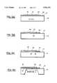
- FIG. 1ais a schematic view of a prior art thermally actuated cantilever microstructure in an open position.
- FIG. 1bis a schematic view of the thermally actuated cantilever microstructure of FIG. 1a, in the closed position.
- FIG. 2ais a schematic view of a prior art piezoelectrically actuated cantilever microstructure, in the closed position.
- FIG. 2bis a schematic view of the prior art cantilever microstructure of FIG. 2a in the open position.
- FIG. 3illustrates a prior art microcantilever which utilizes an electrostatic potential to provide a hold-down force.
- FIG. 4ais a side view of a microshutter structure (in the open position) incorporating the invention hereof.
- FIG. 4bis a side view of a microshutter structure (in the closed position) incorporating the invention hereof.
- FIG. 4cis a plan view of the microshutter structure of FIGS. 4a and 4b.
- FIGS. 5a-5fshow side views of a silicon structure as it is processed to provide the microshutter structure of FIGS. 4a-4c.
- FIG. 6is a schematic side view of a microshutter array which employs a lens to focus an optical beam onto a photosensor.
- FIG. 7is a plan view of an integrated shutter array, such as that employed in FIG. 6.
- FIG. 8is a schematic side view of a shutter arrangement wherein first and second microshutter arrays are employed and the second microshutter array provides optical filtering of illuminating beams gated by the first microshutter array.
- FIG. 9illustrates a schematic of a microshutter array which is illuminated by a collimated beam.
- FIG. 10illustrates an application of a microshutter array incorporating the invention to a color display unit.
- FIG. 11illustrates a plan view of an integrated microshutter array such as that shown in FIG. 10.
- the present inventionuses microcantilevers in a two-dimensional array to construct a microshutter arrangement for optical applications.
- the individual apertures in the arrayare controlled to gate optical, ultraviolet or infrared beams of either coherent (collimated) or non-coherent radiation.
- Individual aperturesare opened and closed using conventional address circuitry which is either synchronously scanned or asynchronously, individually addressable.
- Shutter portions of each microcantilevermay be either opaque or may be constituted by thin film layers which enable selective optical filtering of an illuminating beam.
- the aperture arraycan be controlled to select specific passbands of radiation, at different aperture locations.
- the present inventionemploys cantilever shutters that are comprised of either bimorph or multimorph thin films to enable opening and closing thereof, much like a hinged door over a fixed aperture opening. While thermal actuation is preferred, both piezoelectric and electrostatic-originating forces may also be employed.
- FIGS. 4a-4ca preferred embodiment of a microshutter incorporating the invention hereof will be described.
- a first silicon substrate 12, having an upper oxide layer 14,is adhered to a second silicon substrate 16 which also has an upper oxide layer 18 deposited thereon.
- First silicon layer 12has been etched to provide an aperture A which extends entirely through the thickness of layer 12.
- a microshutter 20includes a proximal portion 22 that is adhered to oxide layer 14.
- a distal portion 24is dimensioned so as to cover aperture A when it is in an unflexed position, such as shown in FIG. 4b. In the flexed position as shown in FIG. 4a, however, microshutter 20 is curled to the left and exposes a region of aperture A where light may transit.
- An aperture Bis etched in silicon substrate 16 and exhibits a lateral dimension which prevents any shadowing of the transmitted beam by microshutter 20 when it is in the flexed position.
- Microshutter 20comprises at least two layers which exhibit different thermal coefficients of expansion (TCE's). As shown in expanded region 30, microshutter 20 includes a low temperature oxide layer 32, a conductive/resistive polysilicon layer 34 and a high temperature silicon nitride (insulating) layer 36. Application of a current to polysilicon layer 34 causes a heating thereof and a concomitant heating of layers 32 and 36. Because the layers exhibit different TCE's, differential expansions occur in each of the layers, with layer 36 expanding more than layer 34, thereby forcing a straightening of microshutter 20 to the right as shown in FIG. 4b. When current is removed from polysilicon layer 34, the resulting cooling of microshutter 20 results in a counterclockwise rotation thereof to a position shown in FIG. 4a.
- TCE'sthermal coefficients of expansion
- polysilicon layer 34can there be seen as having been etched into a serpentine-style resistance region which bridges electrodes 40 and 42. Application of a voltage V2 between contacts 40 and 42 results in a current through polysilicon resistive layer 34 to create the heating action described above.
- a further polysilicon layer 44is positioned about the periphery of microshutter 20 and, when a voltage V1 is applied, provides an electrostatic hold-down force for microshutter 20.
- Layers 32, 34 and 36 of microshutter 20can be made sufficiently thin to be substantially optically transmissive. Under such circumstances, a further film can be deposited thereon which is optically selective to a given wavelength range. Thus, a film can be deposited on the distal shutter region 24 of optical shutter 20 which is selective for the infrared region, the visible region or the ultraviolet region, or to selected wavelengths within one of the aforesaid regions.
- FIGS. 5a-5fthe procedure for fabrication of silicon layer 12 and microshutter 20 will be described.
- silicon substrate 12has already had emplaced thereon (via additive deposition/etch procedures) a silicon nitride layer 36, polysilicon layers 34 and 44, low temperature oxide layer 32 and silicon nitride layer 14.
- low temperature oxide 32is etched to expose the underside of polysilicon layer 44 to enable its subsequent use as an electrostatic hold-down electrode.
- an additional layer of aluminum 50is sputtered onto silicon nitride layer 36 and is patterned to provide access to both polysilicon layers 34 and 44. Thereafter, as shown in FIG. 5d, aperture A is etched in the lowermost surface of silicon substrate 12 to expose silicon nitride layer 14.
- a special fixture deviceis used to protect the front side structures from the etch action.
- a reactive ion etchis applied through aperture A to remove silicon nitride layer 14 from the lowermost surface of low temperature oxide layer 32.
- This actionenables full release of shutter 20 and enables it to curl upwards naturally and to create the normally open condition of the microshutter.
- silicon wafer 16is bonded to the lowermost surface of silicon layer 12 so as to align aperture B with aperture A.
- Lower silicon wafer 16preferably incorporates a metal layer, 52, on top of silicon nitride layer 18 to provide opacity to incident radiation.
- a microshutter array 100is positioned between a source of illumination 102 and a photoreceptor 104.
- a lens 106is positioned to focus light which passes through shutter array 100 onto photoreceptor 104.
- Individual microshutters 108 in microshutter array 100are individually controllable by signals supplied from a connected controller.
- microshutter array 100Details of microshutter array 100 are shown in FIG. 7 wherein a plurality of microshutters 108 are positioned in an array on a substrate 110. XY conductor patterns are positioned on substrate 110 and enable individual selection of a single microshutter 108 or a row or column of microshutters 108. A controller 114 provides cell-select signals to enable operation of one or more of the array-arranged microshutters 108.
- each of the microshutters 122 in microshutter array 120is configured to include an optical filter layer thereon.
- illumination passing through microshutter array 100can be subjected to a filter action or not, in dependence upon control signals applied to individual microshutters 122 in microshutter array 120.
- the cameracan exhibit either a sensitivity to visible light, or to infrared light, as the case may be, dependent upon control signals applied to microshutters 122 in microshutter array 120.
- the effective aperture of the cameracan be controlled.
- FIGS. 6 and 8illustrate the use of an incoherent light source 102 as the source of illumination
- a coherent light source 130may be employed in combination with microshutter array 100 and photoreceptor 104.
- photoreceptor 104preferably comprises plural optical detectors, arrayed to detect the presence or absence of one or more gated, collimated light beams 132, 134, 136, etc. In such manner, the presence or absence of a light beam can be detected and their individual modulations (if any) detected and fed to further demodulation circuitry.
- a microshutter array 100is employed in combination with red, blue and green light emitters 140, 142, and 144.
- a plan view of optical shutter array 100, integrated onto a microchip,is shown in FIG. 11 and includes row/column select circuitry which is operated by controller 146. By selectively gating the red, blue, green cells 140, 142 and 144, a color display can be achieved.
- Each of cells 140, 142 and 144is supported on a substrate (not shown) which is juxtaposed to the lower surface of shutter array 100, thereby creating a flat display configuration.
Landscapes
- Physics & Mathematics (AREA)
- Spectroscopy & Molecular Physics (AREA)
- General Physics & Mathematics (AREA)
- Optics & Photonics (AREA)
- Mechanical Light Control Or Optical Switches (AREA)
Abstract
Description
This invention relates to microstructures that are constructed utilizing semiconductor fabrication processes and, more particularly, to an optical microshutter array produced in accordance with such semiconductor fabrication processes.
Silicon "micromachining" has been developed as a means for accurately fabricating small structures. Such processing involves the selective etching of a silicon substrate and the deposition thereon of thin film layers of semiconductor materials. Various sacrificial layers are employed to enable the fabrication of relatively complex interactive structures.
Silicon micromachining has been applied to the fabrication of micromachines that include rotary and linear bearings. Such bearings have spawned further development of electrically-driven motors which exhibit a planar geometry and lateral dimensions on the order of 100 microns or so. In addition to micromotors, various cantilever structures have also been constructed utilizing micromachining concepts.
FIGS. 1a and 1b illustrate a prior art cantilever device wherein apolysilicon layer 10 is bonded to alayer 12 of different composition. Both layers are attached, at one extremity, to asubstrate 14. The thermal coefficients of expansion ofpolysilicon layer 10 andlayer 12 are chosen as to be sufficiently different that, without an applied potential to create a heating action, the structure exhibits an arcuate form as shown in FIG. 1a. When, as shown in FIG. 1b, a voltage Vt is applied to a resistive portion ofpolysilicon layer 10, current flow causes a heating of both layers and unequal expansion results in a clockwise rotation of the arm until contact is made withsubstrate contact region 16.
The action of the cantilever structure of FIGS. 1a and 1b is much the same as a well known bi-metal thermal actuator widely used in thermostats. Further details of such structures can be found in "Thermally Excited Silicon Microactuators", Riethmuller et al., IEEE Transactions on Electron Devices, Volume 35, No. 6, June 1988, pages 758-763, and in "Design, Fabrication and Testing of a C-Shape Actuator", Lin et al., Proceedings Eighth International Conference on Solid State Sensors and Actuators, Stockholm, Sweden, Jun. 25-29, 1995, pages 418-420.
An example of a thermal actuator comprising a sandwich of polysilicon and gold can be found described in "CMOS Electrothermal Microactuators", Parameswaran et al., Proceedings IEEE Microelectro-Mechanical Systems, 11-14 Feb. 1990, pages 131.
As shown in FIGS. 2a and 2b, cantilever arms have also been constructed using piezoelectric films which exhibit a large d31 characteristic. Such apiezoelectric film 20 has been sandwiched between a pair ofelectrodes contact 26. Application of a voltage Vpz betweenelectrodes contacts
In lieu of constructing a cantilever arm having an unattached free end, other prior art has employed a "tied-down" cantilever structure to provide a buckling action upon actuation by either a piezoelectric force or by a thermally actuated, differential expansion action. For instance, see "A Quantitative Analysis of Scratch Drive Actuator Buckling Motion", Akiyama et al., Proceedings IEEE Micro-Electromechanical Systems, Jan. 29-Feb. 2, 1995, pages 310-315. A further version of such a buckling system is described in "Lateral In-plane Displacement Microactuators with Combined Thermal and Electrostatic Drive", Sun et al., Solid-State Sensor and Actuator Workshop, Hilton Head, Jun. 3-6, 1996, pages 31-34.
Piezoelectrically actuated cantilever micro-devices have been proposed for a variety of applications. Huang et al., in "Piezoelectrically Actuated Microcantilever for Actuated Mirror Array Application", Solid-State Sensor and Actuator Workshop, Hiltonhead Island, S.C., June 3-6, pages 191-195, have suggested the use of a piezoelectrically actuated cantilever structure for control of the orientation of micro-mirrors. Such cantilever structures enable the redirection of an incident light beam to create an optical switching effect.
The application of electrostatic forces to provide both pull-down and repulsive forces in microactuators is known. A structure employing electrostatic forces is shown in FIG. 3, wherein acantilever arm 29 comprises apolysilicon layer 30 affixed to aninsulating layer 32 and spanningsubstrate contacts contact 36 and acrosslayers free end 37 ofcantilever arm 29 andsubstrate contact 36.
Various electrostatically actuated devices can be found described in "Pull-in Dynamics of Electrostatically Actuated Beams", Gupta et al., Poster Session Supplemental Digest, Solid-State Sensor and Actuator Workshop, Hiltonhead Island, South Carolina, Jun. 3-6, 1996,pages 1, 2.
Electrostatic actuation has also been employed to control the action of a microshutter, wherein a moving electrode of aluminum, chromium, gold or doped polysilicon and a fixed counter-electrode is employed. The deflection of the moving electrode is controlled by electrostatic forces. The moving electrode rotates about an axis and employs a torsional-cantilever action. (See "Electrostatically Activated Micro-Shutter in (110) Silicon", Obermeier et al., DSC-Volume 40, Micromechanical Systems ASME, 1992, pages 13-22.
The prior art microshutter described above, because of its use of both torsional and cantilever actions, creates substantial stresses in the supporting cantilever between the shutter portion and the substrate. Further, because a relatively large mass is supported by a relatively thin connecting structure, fatigue failures can be expected to occur in the connecting structure, leading to a shortened lifetime span.
Accordingly, it is an object of this invention to provide an improved microshutter structure.
It is another object of this invention to provide an improved microshutter structure wherein thermal or piezoelectric actuation is employed to accomplish movement of the shutter member.
It is a further object of this invention to provide an improved microshutter, wherein torsional bending forces are avoided.
It is yet another object of this invention to provide an improved microshutter which can be structured in the form of an array and which responds to data signals to selectively transmit or block an illuminating beam.
An optical shutter apparatus includes a source of illumination and a first aperture plate positioned in a path of light from the source of illumination. A cantilever shutter is positioned at each aperture in the aperture plate and includes at least two bonded layers, one being an electrically resistive layer which exhibits a first thermal coefficient of expansion (TCE) and the second layer exhibiting a second TCE that is different from the first TCE. A proximal end of the bonded layers is attached to the aperture plate at each aperture and a distal portion thereof covers the respective aperture when in position thereover. A controller applies signals to the first electrically resistive layer to cause a heating of the first and second layers and a resultant unequal expansion thereof. The expansion causes a flexure of the cantilever shutter and moves the distal portion thereof to either cover or uncover the aperture, which, when uncovered, allows transmission of the illumination therethrough.
FIG. 1a is a schematic view of a prior art thermally actuated cantilever microstructure in an open position.
FIG. 1b is a schematic view of the thermally actuated cantilever microstructure of FIG. 1a, in the closed position.
FIG. 2a is a schematic view of a prior art piezoelectrically actuated cantilever microstructure, in the closed position.
FIG. 2b is a schematic view of the prior art cantilever microstructure of FIG. 2a in the open position.
FIG. 3 illustrates a prior art microcantilever which utilizes an electrostatic potential to provide a hold-down force.
FIG. 4a is a side view of a microshutter structure (in the open position) incorporating the invention hereof.
FIG. 4b is a side view of a microshutter structure (in the closed position) incorporating the invention hereof.
FIG. 4c is a plan view of the microshutter structure of FIGS. 4a and 4b.
FIGS. 5a-5f show side views of a silicon structure as it is processed to provide the microshutter structure of FIGS. 4a-4c.
FIG. 6 is a schematic side view of a microshutter array which employs a lens to focus an optical beam onto a photosensor.
FIG. 7 is a plan view of an integrated shutter array, such as that employed in FIG. 6.
FIG. 8 is a schematic side view of a shutter arrangement wherein first and second microshutter arrays are employed and the second microshutter array provides optical filtering of illuminating beams gated by the first microshutter array.
FIG. 9 illustrates a schematic of a microshutter array which is illuminated by a collimated beam.
FIG. 10 illustrates an application of a microshutter array incorporating the invention to a color display unit.
FIG. 11 illustrates a plan view of an integrated microshutter array such as that shown in FIG. 10.
The present invention uses microcantilevers in a two-dimensional array to construct a microshutter arrangement for optical applications. The individual apertures in the array are controlled to gate optical, ultraviolet or infrared beams of either coherent (collimated) or non-coherent radiation. Individual apertures are opened and closed using conventional address circuitry which is either synchronously scanned or asynchronously, individually addressable. Shutter portions of each microcantilever may be either opaque or may be constituted by thin film layers which enable selective optical filtering of an illuminating beam. The aperture array can be controlled to select specific passbands of radiation, at different aperture locations.
The present invention employs cantilever shutters that are comprised of either bimorph or multimorph thin films to enable opening and closing thereof, much like a hinged door over a fixed aperture opening. While thermal actuation is preferred, both piezoelectric and electrostatic-originating forces may also be employed.
Turning now to FIGS. 4a-4c, a preferred embodiment of a microshutter incorporating the invention hereof will be described. Afirst silicon substrate 12, having anupper oxide layer 14, is adhered to asecond silicon substrate 16 which also has anupper oxide layer 18 deposited thereon.First silicon layer 12 has been etched to provide an aperture A which extends entirely through the thickness oflayer 12.
Amicroshutter 20 includes aproximal portion 22 that is adhered tooxide layer 14. Adistal portion 24 is dimensioned so as to cover aperture A when it is in an unflexed position, such as shown in FIG. 4b. In the flexed position as shown in FIG. 4a, however, microshutter 20 is curled to the left and exposes a region of aperture A where light may transit. An aperture B is etched insilicon substrate 16 and exhibits a lateral dimension which prevents any shadowing of the transmitted beam bymicroshutter 20 when it is in the flexed position.
Turning to FIG. 4(c),polysilicon layer 34 can there be seen as having been etched into a serpentine-style resistance region which bridgeselectrodes contacts polysilicon resistive layer 34 to create the heating action described above. Afurther polysilicon layer 44 is positioned about the periphery ofmicroshutter 20 and, when a voltage V1 is applied, provides an electrostatic hold-down force formicroshutter 20.
More specifically, application of voltage V1 betweenpolysilicon layer 44 and silicon substrate 12 (across insulating layer 14) results in an electrostatic force being applied betweenmicroshutter 20 andsilicon substrate 12 and achieves a hold-down action.
Turning to FIGS. 5a-5f, the procedure for fabrication ofsilicon layer 12 andmicroshutter 20 will be described. Starting with FIG. 5a,silicon substrate 12 has already had emplaced thereon (via additive deposition/etch procedures) asilicon nitride layer 36, polysilicon layers 34 and 44, lowtemperature oxide layer 32 andsilicon nitride layer 14. Next, as shown in FIG. 5b,low temperature oxide 32 is etched to expose the underside ofpolysilicon layer 44 to enable its subsequent use as an electrostatic hold-down electrode.
In FIG. 5c, an additional layer ofaluminum 50 is sputtered ontosilicon nitride layer 36 and is patterned to provide access to bothpolysilicon layers silicon substrate 12 to exposesilicon nitride layer 14. A special fixture device is used to protect the front side structures from the etch action.
Next, as shown in FIG. 5e, a reactive ion etch is applied through aperture A to removesilicon nitride layer 14 from the lowermost surface of lowtemperature oxide layer 32. This action enables full release ofshutter 20 and enables it to curl upwards naturally and to create the normally open condition of the microshutter. Thereafter, as shown in FIG. 5f,silicon wafer 16 is bonded to the lowermost surface ofsilicon layer 12 so as to align aperture B with aperture A.Lower silicon wafer 16 preferably incorporates a metal layer, 52, on top ofsilicon nitride layer 18 to provide opacity to incident radiation.
Referring now to FIGS. 6-11, structures incorporating microshutter arrays employing the invention, will be described. In FIG. 6, amicroshutter array 100 is positioned between a source ofillumination 102 and aphotoreceptor 104. Alens 106 is positioned to focus light which passes throughshutter array 100 ontophotoreceptor 104.Individual microshutters 108 inmicroshutter array 100 are individually controllable by signals supplied from a connected controller.
Details ofmicroshutter array 100 are shown in FIG. 7 wherein a plurality ofmicroshutters 108 are positioned in an array on asubstrate 110. XY conductor patterns are positioned onsubstrate 110 and enable individual selection of asingle microshutter 108 or a row or column ofmicroshutters 108. Acontroller 114 provides cell-select signals to enable operation of one or more of the array-arrangedmicroshutters 108.
In FIG. 8, the microshutter structure shown in FIG. 6 has been modified by inclusion of anadditional microshutter array 120. In this instance, each of the microshutters 122 inmicroshutter array 120 is configured to include an optical filter layer thereon. Thus, by appropriately controllingmicroshutter array 120, illumination passing throughmicroshutter array 100 can be subjected to a filter action or not, in dependence upon control signals applied toindividual microshutters 122 inmicroshutter array 120. Thus, ifmicroshutter arrays microshutters 122 inmicroshutter array 120. Further, by appropriately opening or closing the individual microshutters inmicroshutter array 100, the effective aperture of the camera can be controlled.
While FIGS. 6 and 8 illustrate the use of an incoherentlight source 102 as the source of illumination, a coherentlight source 130, as shown in FIG. 9, may be employed in combination withmicroshutter array 100 andphotoreceptor 104. Under such conditions,photoreceptor 104 preferably comprises plural optical detectors, arrayed to detect the presence or absence of one or more gated, collimatedlight beams
In FIG. 10, amicroshutter array 100 is employed in combination with red, blue andgreen light emitters optical shutter array 100, integrated onto a microchip, is shown in FIG. 11 and includes row/column select circuitry which is operated bycontroller 146. By selectively gating the red, blue,green cells cells shutter array 100, thereby creating a flat display configuration.
It should be understood that the foregoing description is only illustrative of the invention. Various alternatives and modifications can be devised by those skilled in the art without departing from the invention. Accordingly, the present invention is intended to embrace all such alternatives, modifications and variances which fall within the scope of the appended claims.
Claims (20)
1. An optical shutter apparatus comprising:
a source of illumination;
a first aperture plate positioned in a path of light from said source of illumination and including plural apertures;
a cantilever shutter positioned at each of said apertures, each cantilever shutter comprising;
at least two bonded layers including a first, electrically resistive layer exhibiting a first thermal coefficient of expansion (TCE) and a second layer exhibiting a second TCE that is different from said first TCE;
a proximal end attached to said aperture plate adjacent an aperture and a distal portion sized to cover said aperture when in position thereover; and
control means for applying a signal to said first electrically resistive layer to cause a heating of said layers and a resultant unequal expansion thereof to cause a flexure therein which moves said distal portion to either cover or uncover said aperture, when uncovered, allowing transmission of said illumination therethrough.
2. The optical shutter apparatus as recited in claim 1, wherein a conductive layer is positioned on said second layer and (ii) said first aperture plate is at least partially conductive,
said control means applying a dc potential between said aperture plate and said conductive layer when said aperture is covered to exert an electrostatic hold-down force on said distal portion of said cantilever shutter.
3. The optical shutter apparatus as recited in claim 1, wherein said first layer exhibits a thinner thickness in said distal portion than a thickness of said second layer in said distal portion to enable a greater flexure of said distal portion upon said heating.
4. The optical shutter apparatus as recited in claim 1, wherein said first aperture plate is comprised of first and second silicon layers, an aperture opening in said second silicon layer exhibiting a lesser cross-section than a co-located aperture opening in said first silicon layer.
5. The optical shutter apparatus as recited in claim 1, wherein said first aperture plate comprises an array of said apertures and said control means selectively open or closes individual ones of said apertures in accordance with data states.
6. The optical shutter apparatus as recited in claim 5, wherein said array of said apertures is one dimensional.
7. The optical shutter apparatus as recited in claim 5, wherein said array of said apertures is two dimensional.
8. The optical shutter apparatus as recited in claim 5, further comprising:
an array of photodetectors for detecting illumination transmitted through said apertures.
9. The optical shutter apparatus as recited in claim 5, further comprising:
a second aperture plate aligned with said first aperture plate and including a cantilever shutter at each aperture therein, each cantilever shutter in said second aperture plate including a distal portion which is at least partially transmissive of said illumination, but provides a filter action upon said illumination,
said control means further operative to selectively open or close individual ones of said cantilever shutters in said second aperture plate in accordance with data states.
10. The optical shutter apparatus as recited in claim 9, wherein said filter action selectively passes illumination in one of: infra-red, visible and ultra-violet optical ranges.
11. The optical shutter apparatus as recited in claim 9, further comprising:
optical detection means for responding to incident illumination;
lens means positioned between said second aperture plate and said optical detection means for focussing illumination transmitted through said first aperture plate and second aperture plate onto said optical detection means.
12. The optical shutter apparatus as recited in claim 5, further comprising:
optical detection means for responding to incident illumination;
lens means positioned between said first aperture plate and said optical detection means for focussing illumination transmitted through said first aperture plate onto said optical detection means.
13. An optical shutter apparatus comprising:
a source of illumination;
a first aperture plate positioned in a path of light from said source of illumination and including plural apertures;
a cantilever shutter positioned at each of said apertures, each cantilever shutter comprising;
plural bonded layers including a first layer, and second and third piezoelectric layers arranged about said first layer in a sandwich fashion;
a proximal end attached to said aperture plate adjacent an aperture and a distal portion sized to cover said aperture when in position thereover; and
control means for applying signals to said second and third piezoelectric layers to cause relative movement between said second and third layers and said first layer, resulting in a flexure of said cantilever shutter which moves said distal portion to either cover or uncover said aperture, said aperture, when uncovered, allowing transmission of said illumination therethrough.
14. The optical shutter apparatus as recited in claim 13, wherein a conductive layer is positioned on said cantilever shutter and (ii) said first aperture plate is at least partially conductive,
said control means applying a dc potential between said aperture plate and said conductive layer when said aperture is covered to exert an electrostatic hold-down force on said distal portion of said cantilever shutter.
15. The optical shutter apparatus as recited in claim 13, wherein said second piezoelectric layer exhibits a thinner thickness than a thickness of said third piezoelectric layer portion to enable a flexure of said distal portion towards said second piezoelectric layer upon application of said signals.
16. The optical shutter apparatus as recited in claim 13, wherein said first aperture plate is comprised of first and second silicon layers, an aperture opening in said second silicon layer exhibiting a lesser cross-section than a co-located aperture opening in said first silicon layer.
17. The optical shutter apparatus as recited in claim 13, wherein said first aperture plate comprises an array of said apertures and said control means selectively open or closes individual ones of said apertures in accordance with data states.
18. The optical shutter apparatus as recited in claim 17, wherein said array of said apertures is one dimensional.
19. The optical shutter apparatus as recited in claim 17, wherein said array of said apertures is two dimensional.
20. The optical shutter apparatus as recited in claim 13, further comprising:
an array of photoreceptor for detecting illumination transmitted through said apertures.
Priority Applications (1)
| Application Number | Priority Date | Filing Date | Title |
|---|---|---|---|
| US08/787,307US5781331A (en) | 1997-01-24 | 1997-01-24 | Optical microshutter array |
Applications Claiming Priority (1)
| Application Number | Priority Date | Filing Date | Title |
|---|---|---|---|
| US08/787,307US5781331A (en) | 1997-01-24 | 1997-01-24 | Optical microshutter array |
Publications (1)
| Publication Number | Publication Date |
|---|---|
| US5781331Atrue US5781331A (en) | 1998-07-14 |
Family
ID=25141069
Family Applications (1)
| Application Number | Title | Priority Date | Filing Date |
|---|---|---|---|
| US08/787,307Expired - Fee RelatedUS5781331A (en) | 1997-01-24 | 1997-01-24 | Optical microshutter array |
Country Status (1)
| Country | Link |
|---|---|
| US (1) | US5781331A (en) |
Cited By (142)
| Publication number | Priority date | Publication date | Assignee | Title |
|---|---|---|---|---|
| US6017770A (en)* | 1998-09-30 | 2000-01-25 | Eastman Kodak Company | Method of making a hybrid micro-electromagnetic article of manufacture |
| US6046837A (en)* | 1997-12-08 | 2000-04-04 | Fuji Photo Film Co., Ltd. | Optical modulator |
| US6067183A (en)* | 1998-12-09 | 2000-05-23 | Eastman Kodak Company | Light modulator with specific electrode configurations |
| US6075239A (en)* | 1997-09-10 | 2000-06-13 | Lucent Technologies, Inc. | Article comprising a light-actuated micromechanical photonic switch |
| DE19932488A1 (en)* | 1999-07-09 | 2001-02-08 | Epigenomics Gmbh | Photographic illumination apparatus for biological matter has a perforated mask between the light source and the DNA chip with micro shutters operated by electronic control |
| US6226116B1 (en)* | 1999-11-30 | 2001-05-01 | Eastman Kodak Company | Magnetic micro-shutters |
| US6249370B1 (en)* | 1998-09-18 | 2001-06-19 | Ngk Insulators, Ltd. | Display device |
| US6248509B1 (en) | 1999-07-27 | 2001-06-19 | James E. Sanford | Maskless photoresist exposure system using mems devices |
| US6268908B1 (en)* | 1999-08-30 | 2001-07-31 | International Business Machines Corporation | Micro adjustable illumination aperture |
| US6275320B1 (en)* | 1999-09-27 | 2001-08-14 | Jds Uniphase, Inc. | MEMS variable optical attenuator |
| WO2001065302A1 (en)* | 2000-03-03 | 2001-09-07 | Axsun Technologies, Inc. | Optical switch array using rolling shutter optical switch elements |
| US6325554B1 (en) | 2000-03-15 | 2001-12-04 | Eastman Kodak Company | Camera with electrostatic light valve that functions as image reflecting mirror for viewfinder |
| EP1126305A3 (en)* | 2000-02-16 | 2002-01-23 | C.R.F. Società Consortile per Azioni | Electrostatic microshutter matrix having a high fill factor |
| US6389189B1 (en) | 1998-10-23 | 2002-05-14 | Corning Incorporated | Fluid-encapsulated MEMS optical switch |
| US6404942B1 (en) | 1998-10-23 | 2002-06-11 | Corning Incorporated | Fluid-encapsulated MEMS optical switch |
| US6410361B2 (en)* | 1999-09-13 | 2002-06-25 | Jds Uniphase Corporation | Methods of fabricating in-plane MEMS thermal actuators |
| US6430333B1 (en)* | 1999-04-15 | 2002-08-06 | Solus Micro Technologies, Inc. | Monolithic 2D optical switch and method of fabrication |
| WO2002061486A1 (en)* | 2000-12-19 | 2002-08-08 | Coventor, Incorporated | Bulk micromachining process for fabricating an optical mems device with integrated optical aperture |
| US6438954B1 (en)* | 2001-04-27 | 2002-08-27 | 3M Innovative Properties Company | Multi-directional thermal actuator |
| US6443637B1 (en) | 2000-03-15 | 2002-09-03 | Eastman Kodak Company | Camera with electrostatic light valve that functions as diaphragm |
| US6477303B1 (en) | 2000-05-15 | 2002-11-05 | Litton Systems, Inc. | MEMS optical backplane interface |
| US20020170290A1 (en)* | 2001-05-18 | 2002-11-21 | Victor Bright | Multi-dimensional micro-electromechanical assemblies and method of making same |
| US6535318B1 (en)* | 1999-11-12 | 2003-03-18 | Jds Uniphase Corporation | Integrated optoelectronic devices having pop-up mirrors therein and methods of forming and operating same |
| US20030058515A1 (en)* | 1999-07-27 | 2003-03-27 | Sanford James E. | MEMS-based valve device |
| US6587626B2 (en) | 2000-03-23 | 2003-07-01 | Corning Incorporated | Liquid overclad-encapsulated optical device |
| EP1329319A1 (en)* | 2002-01-17 | 2003-07-23 | Eastman Kodak Company | Thermal actuator with optimized heater length |
| EP1022598A3 (en)* | 1999-01-20 | 2003-10-01 | Fuji Photo Film Co., Ltd. | Light modulation element, drive method thereof, and flat-panel display unit |
| US20030184189A1 (en)* | 2002-03-29 | 2003-10-02 | Sinclair Michael J. | Electrostatic bimorph actuator |
| US6643426B1 (en) | 1999-10-19 | 2003-11-04 | Corning Incorporated | Mechanically assisted release for MEMS optical switch |
| EP1334831A3 (en)* | 2002-02-08 | 2004-01-07 | Eastman Kodak Company | Dual actuation thermal actuator and method of operating thereof |
| EP1241507A3 (en)* | 2001-03-16 | 2004-01-14 | C.R.F. Società Consortile per Azioni | An electrostatically-controlled optical micro-shutter with non-transparent fixed electrode |
| US6691513B1 (en)* | 2002-08-16 | 2004-02-17 | Pc Lens Corporation | System and method for providing an improved electrothermal actuator for a micro-electro-mechanical device |
| US20040085535A1 (en)* | 2000-02-15 | 2004-05-06 | Hammer Michael R. | Optical shutter for spectroscopy instrument |
| US6738338B1 (en)* | 1999-03-17 | 2004-05-18 | Seiko Instruments Inc. | Near-field optical head, method of fabricating same, and optical drive using same |
| EP1364792A3 (en)* | 2002-05-23 | 2004-05-19 | Eastman Kodak Company | Multi-layer thermal actuator with optimized heater length and method of operating same |
| US6770882B2 (en) | 2002-01-14 | 2004-08-03 | Multispectral Imaging, Inc. | Micromachined pyro-optical structure |
| US6775048B1 (en)* | 2000-10-31 | 2004-08-10 | Microsoft Corporation | Microelectrical mechanical structure (MEMS) optical modulator and optical display system |
| US20040195510A1 (en)* | 2003-02-07 | 2004-10-07 | Carr William N. | Radiation sensor with synchronous reset |
| US20050011191A1 (en)* | 2001-12-31 | 2005-01-20 | Microsoft Corporation | Unilateral thermal buckle beam actuator |
| US6867897B2 (en)* | 2003-01-29 | 2005-03-15 | Reflectivity, Inc | Micromirrors and off-diagonal hinge structures for micromirror arrays in projection displays |
| US6877316B1 (en)* | 2003-11-21 | 2005-04-12 | Zyvex Corporation | Electro-thermal scratch drive actuator |
| US20050134855A1 (en)* | 2003-12-23 | 2005-06-23 | C.R.F. Societa Consortile Per Azioni | Spectrophotometer with micro-filters |
| US20050133479A1 (en)* | 2003-12-19 | 2005-06-23 | Youngner Dan W. | Equipment and process for creating a custom sloped etch in a substrate |
| US20060033977A1 (en)* | 2003-02-12 | 2006-02-16 | Patel Satyadev R | Micromirror device |
| US20060072224A1 (en)* | 2000-04-07 | 2006-04-06 | Microsoft Corporation | Magnetically actuated microelectromechanical systems actuator |
| WO2005104717A3 (en)* | 2004-04-23 | 2006-04-27 | David E Dausch | Flexible electrostatic actuator |
| US20060187529A1 (en)* | 2005-02-23 | 2006-08-24 | Pixtronix, Incorporated | Display methods and apparatus |
| US20060187530A1 (en)* | 2005-02-23 | 2006-08-24 | Pixtronix, Incorporated | Methods and apparatus for actuating displays |
| US20060227184A1 (en)* | 1997-07-15 | 2006-10-12 | Silverbrook Research Pty Ltd | Micro-electromechanical valve having transformable valve actuator |
| KR100687606B1 (en) | 2004-11-12 | 2007-02-27 | 한국과학기술원 | Light valve having a movable thin film and display device using the same |
| US20070146900A1 (en)* | 2005-12-08 | 2007-06-28 | Jorg Steinert | Diaphragm device |
| US7304786B2 (en) | 2005-02-23 | 2007-12-04 | Pixtronix, Inc. | Methods and apparatus for bi-stable actuation of displays |
| US20080062500A1 (en)* | 2005-02-23 | 2008-03-13 | Pixtronix, Inc. | Methods and apparatus for spatial light modulation |
| US20080158635A1 (en)* | 2005-02-23 | 2008-07-03 | Pixtronix, Inc. | Display apparatus and methods for manufacture thereof |
| US7405852B2 (en) | 2005-02-23 | 2008-07-29 | Pixtronix, Inc. | Display apparatus and methods for manufacture thereof |
| US20080201665A1 (en)* | 2007-02-15 | 2008-08-21 | Teac Corporation | Electronic equipment having plural function keys |
| WO2008112713A1 (en)* | 2007-03-13 | 2008-09-18 | Nanoink, Inc. | Nanolithography with use of viewports |
| CN100451737C (en)* | 2004-04-23 | 2009-01-14 | 研究三角协会 | Flexible electrostatic actuator |
| US7502159B2 (en) | 2005-02-23 | 2009-03-10 | Pixtronix, Inc. | Methods and apparatus for actuating displays |
| US20090142050A1 (en)* | 2007-11-29 | 2009-06-04 | Samsung Electronics Co., Ltd. | Micro shutter having iris function, method for manufacturing the same, and micro camera module having the same |
| US20090244678A1 (en)* | 2005-02-23 | 2009-10-01 | Pixtronix, Inc. | Display apparatus and methods for manufacture thereof |
| US7616368B2 (en) | 2005-02-23 | 2009-11-10 | Pixtronix, Inc. | Light concentrating reflective display methods and apparatus |
| US20100027100A1 (en)* | 2008-08-04 | 2010-02-04 | Pixtronix, Inc. | Display with controlled formation of bubbles |
| US7675665B2 (en) | 2005-02-23 | 2010-03-09 | Pixtronix, Incorporated | Methods and apparatus for actuating displays |
| US20100110518A1 (en)* | 2008-10-27 | 2010-05-06 | Pixtronix, Inc. | Mems anchors |
| US7742016B2 (en) | 2005-02-23 | 2010-06-22 | Pixtronix, Incorporated | Display methods and apparatus |
| US7746529B2 (en) | 2005-02-23 | 2010-06-29 | Pixtronix, Inc. | MEMS display apparatus |
| US7755582B2 (en) | 2005-02-23 | 2010-07-13 | Pixtronix, Incorporated | Display methods and apparatus |
| US20100290101A1 (en)* | 2009-05-13 | 2010-11-18 | Samsung Electronics Co., Ltd. | Light screening device and manufacturing method thereof |
| US7839356B2 (en) | 2005-02-23 | 2010-11-23 | Pixtronix, Incorporated | Display methods and apparatus |
| US7852546B2 (en) | 2007-10-19 | 2010-12-14 | Pixtronix, Inc. | Spacers for maintaining display apparatus alignment |
| US7876489B2 (en) | 2006-06-05 | 2011-01-25 | Pixtronix, Inc. | Display apparatus with optical cavities |
| US7950777B2 (en) | 1997-07-15 | 2011-05-31 | Silverbrook Research Pty Ltd | Ejection nozzle assembly |
| US20110170158A1 (en)* | 2010-01-08 | 2011-07-14 | Samsung Electronics Co., Ltd. | Optical shuttering device and method of manufacturing the same |
| US8020970B2 (en) | 1997-07-15 | 2011-09-20 | Silverbrook Research Pty Ltd | Printhead nozzle arrangements with magnetic paddle actuators |
| US8025366B2 (en) | 1997-07-15 | 2011-09-27 | Silverbrook Research Pty Ltd | Inkjet printhead with nozzle layer defining etchant holes |
| US8029102B2 (en) | 1997-07-15 | 2011-10-04 | Silverbrook Research Pty Ltd | Printhead having relatively dimensioned ejection ports and arms |
| US8029101B2 (en) | 1997-07-15 | 2011-10-04 | Silverbrook Research Pty Ltd | Ink ejection mechanism with thermal actuator coil |
| US8061812B2 (en) | 1997-07-15 | 2011-11-22 | Silverbrook Research Pty Ltd | Ejection nozzle arrangement having dynamic and static structures |
| US8075104B2 (en) | 1997-07-15 | 2011-12-13 | Sliverbrook Research Pty Ltd | Printhead nozzle having heater of higher resistance than contacts |
| US8083326B2 (en) | 1997-07-15 | 2011-12-27 | Silverbrook Research Pty Ltd | Nozzle arrangement with an actuator having iris vanes |
| WO2012018483A1 (en)* | 2010-07-26 | 2012-02-09 | Qualcomm Mems Technologies, Inc. | Mems-based aperture and shutter |
| US8113629B2 (en) | 1997-07-15 | 2012-02-14 | Silverbrook Research Pty Ltd. | Inkjet printhead integrated circuit incorporating fulcrum assisted ink ejection actuator |
| US8123336B2 (en) | 1997-07-15 | 2012-02-28 | Silverbrook Research Pty Ltd | Printhead micro-electromechanical nozzle arrangement with motion-transmitting structure |
| US8159428B2 (en) | 2005-02-23 | 2012-04-17 | Pixtronix, Inc. | Display methods and apparatus |
| US8168120B1 (en) | 2007-03-06 | 2012-05-01 | The Research Foundation Of State University Of New York | Reliable switch that is triggered by the detection of a specific gas or substance |
| US8248560B2 (en) | 2008-04-18 | 2012-08-21 | Pixtronix, Inc. | Light guides and backlight systems incorporating prismatic structures and light redirectors |
| US8262274B2 (en) | 2006-10-20 | 2012-09-11 | Pitronix, Inc. | Light guides and backlight systems incorporating light redirectors at varying densities |
| US8310442B2 (en) | 2005-02-23 | 2012-11-13 | Pixtronix, Inc. | Circuits for controlling display apparatus |
| WO2012165745A1 (en)* | 2011-06-01 | 2012-12-06 | 한국과학기술원 | Display device |
| US20120328281A1 (en)* | 2011-06-24 | 2012-12-27 | Samsung Electronics Co., Ltd. | Light screening apparatus and fabricating method thereof |
| KR101235627B1 (en) | 2010-09-02 | 2013-02-21 | 한국과학기술원 | Apparatus for display |
| EP2583936A1 (en)* | 2011-10-21 | 2013-04-24 | Raytheon Company | Optical air slit and method for manufacturing optical air slits |
| US8482496B2 (en) | 2006-01-06 | 2013-07-09 | Pixtronix, Inc. | Circuits for controlling MEMS display apparatus on a transparent substrate |
| US8520285B2 (en) | 2008-08-04 | 2013-08-27 | Pixtronix, Inc. | Methods for manufacturing cold seal fluid-filled display apparatus |
| US8519945B2 (en) | 2006-01-06 | 2013-08-27 | Pixtronix, Inc. | Circuits for controlling display apparatus |
| US8526096B2 (en) | 2006-02-23 | 2013-09-03 | Pixtronix, Inc. | Mechanical light modulators with stressed beams |
| US20130259439A1 (en)* | 2012-03-30 | 2013-10-03 | Sumitomo Electric Device Innovations, Inc. | Optical device |
| CN103926755A (en)* | 2013-12-30 | 2014-07-16 | 厦门天马微电子有限公司 | Display and manufacturing method thereof |
| WO2014107634A3 (en)* | 2013-01-05 | 2014-09-12 | Tinz Optics, Inc. | Apparatus for use of multiple optical chains |
| US9063332B2 (en) | 2010-12-17 | 2015-06-23 | Samsung Electronics Co., Ltd. | Light screening apparatus and electronic device including the same |
| US9082353B2 (en) | 2010-01-05 | 2015-07-14 | Pixtronix, Inc. | Circuits for controlling display apparatus |
| US9087486B2 (en) | 2005-02-23 | 2015-07-21 | Pixtronix, Inc. | Circuits for controlling display apparatus |
| US9135868B2 (en) | 2005-02-23 | 2015-09-15 | Pixtronix, Inc. | Direct-view MEMS display devices and methods for generating images thereon |
| US9134552B2 (en) | 2013-03-13 | 2015-09-15 | Pixtronix, Inc. | Display apparatus with narrow gap electrostatic actuators |
| US9170421B2 (en) | 2013-02-05 | 2015-10-27 | Pixtronix, Inc. | Display apparatus incorporating multi-level shutters |
| US9176318B2 (en) | 2007-05-18 | 2015-11-03 | Pixtronix, Inc. | Methods for manufacturing fluid-filled MEMS displays |
| US9197816B2 (en) | 2013-10-18 | 2015-11-24 | The Lightco Inc. | Zoom related methods and apparatus |
| CN105161022A (en)* | 2015-10-22 | 2015-12-16 | 厦门天马微电子有限公司 | Displayer and manufacturing method thereof |
| US9229222B2 (en) | 2005-02-23 | 2016-01-05 | Pixtronix, Inc. | Alignment methods in fluid-filled MEMS displays |
| CN105259676A (en)* | 2015-11-18 | 2016-01-20 | 厦门天马微电子有限公司 | Array substrate, display panel and manufacturing method of array substrate |
| US9261694B2 (en) | 2005-02-23 | 2016-02-16 | Pixtronix, Inc. | Display apparatus and methods for manufacture thereof |
| US9291813B2 (en) | 2010-12-20 | 2016-03-22 | Pixtronix, Inc. | Systems and methods for MEMS light modulator arrays with reduced acoustic emission |
| US9374514B2 (en) | 2013-10-18 | 2016-06-21 | The Lightco Inc. | Methods and apparatus relating to a camera including multiple optical chains |
| US9426365B2 (en) | 2013-11-01 | 2016-08-23 | The Lightco Inc. | Image stabilization related methods and apparatus |
| US9423588B2 (en) | 2013-10-18 | 2016-08-23 | The Lightco Inc. | Methods and apparatus for supporting zoom operations |
| US9462170B2 (en) | 2014-02-21 | 2016-10-04 | The Lightco Inc. | Lighting methods and apparatus |
| US9467627B2 (en) | 2013-10-26 | 2016-10-11 | The Lightco Inc. | Methods and apparatus for use with multiple optical chains |
| US9544503B2 (en) | 2014-12-30 | 2017-01-10 | Light Labs Inc. | Exposure control methods and apparatus |
| US9554031B2 (en) | 2013-12-31 | 2017-01-24 | Light Labs Inc. | Camera focusing related methods and apparatus |
| US9736365B2 (en) | 2013-10-26 | 2017-08-15 | Light Labs Inc. | Zoom related methods and apparatus |
| US9749549B2 (en) | 2015-10-06 | 2017-08-29 | Light Labs Inc. | Methods and apparatus for facilitating selective blurring of one or more image portions |
| US9824427B2 (en) | 2015-04-15 | 2017-11-21 | Light Labs Inc. | Methods and apparatus for generating a sharp image |
| US9857584B2 (en) | 2015-04-17 | 2018-01-02 | Light Labs Inc. | Camera device methods, apparatus and components |
| US9912864B2 (en) | 2014-10-17 | 2018-03-06 | Light Labs Inc. | Methods and apparatus for using a camera device to support multiple modes of operation |
| US9930233B2 (en) | 2015-04-22 | 2018-03-27 | Light Labs Inc. | Filter mounting methods and apparatus and related camera apparatus |
| US9948832B2 (en) | 2016-06-22 | 2018-04-17 | Light Labs Inc. | Methods and apparatus for synchronized image capture in a device including optical chains with different orientations |
| US9967535B2 (en) | 2015-04-17 | 2018-05-08 | Light Labs Inc. | Methods and apparatus for reducing noise in images |
| US9979878B2 (en) | 2014-02-21 | 2018-05-22 | Light Labs Inc. | Intuitive camera user interface methods and apparatus |
| US9998638B2 (en) | 2014-12-17 | 2018-06-12 | Light Labs Inc. | Methods and apparatus for implementing and using camera devices |
| US10003738B2 (en) | 2015-12-18 | 2018-06-19 | Light Labs Inc. | Methods and apparatus for detecting and/or indicating a blocked sensor or camera module |
| US10075651B2 (en) | 2015-04-17 | 2018-09-11 | Light Labs Inc. | Methods and apparatus for capturing images using multiple camera modules in an efficient manner |
| US10091447B2 (en) | 2015-04-17 | 2018-10-02 | Light Labs Inc. | Methods and apparatus for synchronizing readout of multiple image sensors |
| US10094982B2 (en) | 2015-03-11 | 2018-10-09 | Parker-Hannifin Corporation | Passive optical circuit breaker having plural optical waveguide portions with different transmissivities |
| US10110794B2 (en) | 2014-07-09 | 2018-10-23 | Light Labs Inc. | Camera device including multiple optical chains and related methods |
| US10129483B2 (en) | 2015-06-23 | 2018-11-13 | Light Labs Inc. | Methods and apparatus for implementing zoom using one or more moveable camera modules |
| US10191356B2 (en) | 2014-07-04 | 2019-01-29 | Light Labs Inc. | Methods and apparatus relating to detection and/or indicating a dirty lens condition |
| US10225445B2 (en) | 2015-12-18 | 2019-03-05 | Light Labs Inc. | Methods and apparatus for providing a camera lens or viewing point indicator |
| US10306218B2 (en) | 2016-03-22 | 2019-05-28 | Light Labs Inc. | Camera calibration apparatus and methods |
| US10365480B2 (en) | 2015-08-27 | 2019-07-30 | Light Labs Inc. | Methods and apparatus for implementing and/or using camera devices with one or more light redirection devices |
| US10491806B2 (en) | 2015-08-03 | 2019-11-26 | Light Labs Inc. | Camera device control related methods and apparatus |
| US10976493B2 (en)* | 2014-04-30 | 2021-04-13 | Hewlett Packard Enterprise Development Lp | Controllable diamond waveguide tuner |
Citations (6)
| Publication number | Priority date | Publication date | Assignee | Title |
|---|---|---|---|---|
| US3463572A (en)* | 1966-10-21 | 1969-08-26 | Perkin Elmer Corp | Optical phase modulation apparatus |
| US3746785A (en)* | 1971-11-26 | 1973-07-17 | Bendix Corp | Deflectable membrane optical modulator |
| US4698602A (en)* | 1985-10-09 | 1987-10-06 | The United States Of America As Represented By The Secretary Of The Air Force | Micromirror spatial light modulator |
| US4786149A (en)* | 1986-05-22 | 1988-11-22 | Siemens Aktiengesellschaft | Arrangement for optical image processing |
| US5424866A (en)* | 1991-01-30 | 1995-06-13 | Kikinis; Dan | Dynamic holographic display with cantilever |
| US5659418A (en)* | 1996-02-05 | 1997-08-19 | Lucent Technologies Inc. | Structure for membrane damping in a micromechanical modulator |
- 1997
- 1997-01-24USUS08/787,307patent/US5781331A/ennot_activeExpired - Fee Related
Patent Citations (6)
| Publication number | Priority date | Publication date | Assignee | Title |
|---|---|---|---|---|
| US3463572A (en)* | 1966-10-21 | 1969-08-26 | Perkin Elmer Corp | Optical phase modulation apparatus |
| US3746785A (en)* | 1971-11-26 | 1973-07-17 | Bendix Corp | Deflectable membrane optical modulator |
| US4698602A (en)* | 1985-10-09 | 1987-10-06 | The United States Of America As Represented By The Secretary Of The Air Force | Micromirror spatial light modulator |
| US4786149A (en)* | 1986-05-22 | 1988-11-22 | Siemens Aktiengesellschaft | Arrangement for optical image processing |
| US5424866A (en)* | 1991-01-30 | 1995-06-13 | Kikinis; Dan | Dynamic holographic display with cantilever |
| US5659418A (en)* | 1996-02-05 | 1997-08-19 | Lucent Technologies Inc. | Structure for membrane damping in a micromechanical modulator |
Non-Patent Citations (16)
| Title |
|---|
| IEEE Proceedings Micro Electro Mechanical Systems, 1990, pp. 128 131, M. Parameswaran et al., CMOS Electrothermal Microactuators .* |
| IEEE Proceedings Micro Electro Mechanical Systems, 1995, pp. 310 315, Terunobu Akiyama et al., A Quantitive Analysis of Scratch Drive Actuator Using Buckling Motion .* |
| IEEE Proceedings-Micro Electro Mechanical Systems, 1990, pp. 128-131, M. Parameswaran et al., "CMOS Electrothermal Microactuators". |
| IEEE Proceedings-Micro Electro Mechanical Systems, 1995, pp. 310-315, Terunobu Akiyama et al., "A Quantitive Analysis of Scratch Drive Actuator Using Buckling Motion". |
| IEEE Transactions on Electron Devices, vol. 35, No. 6, Jun. 1988, pp. 758 763, Werner Riethm u ller et al., Thermally Excited Silicon Microactuators .* |
| IEEE Transactions on Electron Devices, vol. 35, No. 6, Jun. 1988, pp. 758-763, Werner Riethmuller et al., "Thermally Excited Silicon Microactuators". |
| Late News Poster Session Supplemental Digest Solid State Sensor and Actuator Workshop, Jun. 1996, pp. 1 2, R. K. Gupta et al., Pull In Dynamics of Electrostatically Actuated Beams .* |
| Late-News Poster Session Supplemental Digest-Solid-State Sensor and Actuator Workshop, Jun. 1996, pp. 1-2, R. K. Gupta et al., "Pull-In Dynamics of Electrostatically-Actuated Beams". |
| Symposium on Micromechanical Systems, DSC vol. 40, 1992, pp. 13 23, E. Obermeier et al., Electrostatically Activated Micro Shutter In (110) Silicon .* |
| Symposium on Micromechanical Systems, DSC-vol. 40, 1992, pp. 13-23, E. Obermeier et al., "Electrostatically Activated Micro-Shutter In (110) Silicon". |
| Technical Digest Solid State Sensor and Actuator Workshop, Jun. 1996, pp. 191 195, Yongli Huang et al., Piezoelectrically Actuated Microcantilever for Actuated Mirror Array Application .* |
| Technical Digest Solid State Sensor and Actuator Workshop, Jun. 1996, pp. 31 35, Sun et al., Lateral In Plane Displacement Microactuators with Combined Thermal and Electrostatic Drive .* |
| Technical Digest-Solid-State Sensor and Actuator Workshop, Jun. 1996, pp. 191-195, Yongli Huang et al., "Piezoelectrically Actuated Microcantilever for Actuated Mirror Array Application". |
| Technical Digest-Solid-State Sensor and Actuator Workshop, Jun. 1996, pp. 31-35, Sun et al., "Lateral In-Plane Displacement Microactuators with Combined Thermal and Electrostatic Drive". |
| The Eighth International Conference on Solid State Sensors and Actuators, and Eurosensors IX, Jun. 1996, pp. 416 419, G. Lin et al., Design, Fabrication, and Testing of a C Shaped Actuator .* |
| The Eighth International Conference on Solid-State Sensors and Actuators, and Eurosensors IX, Jun. 1996, pp. 416-419, G. Lin et al., "Design, Fabrication, and Testing of a C-Shaped Actuator". |
Cited By (247)
| Publication number | Priority date | Publication date | Assignee | Title |
|---|---|---|---|---|
| US7357488B2 (en) | 1997-07-15 | 2008-04-15 | Silverbrook Research Pty Ltd | Nozzle assembly incorporating a shuttered actuation mechanism |
| US8113629B2 (en) | 1997-07-15 | 2012-02-14 | Silverbrook Research Pty Ltd. | Inkjet printhead integrated circuit incorporating fulcrum assisted ink ejection actuator |
| US20060227184A1 (en)* | 1997-07-15 | 2006-10-12 | Silverbrook Research Pty Ltd | Micro-electromechanical valve having transformable valve actuator |
| US8020970B2 (en) | 1997-07-15 | 2011-09-20 | Silverbrook Research Pty Ltd | Printhead nozzle arrangements with magnetic paddle actuators |
| US7152960B2 (en)* | 1997-07-15 | 2006-12-26 | Silverbrook Research Pty Ltd | Micro-electromechanical valve having transformable valve actuator |
| US8123336B2 (en) | 1997-07-15 | 2012-02-28 | Silverbrook Research Pty Ltd | Printhead micro-electromechanical nozzle arrangement with motion-transmitting structure |
| US7950777B2 (en) | 1997-07-15 | 2011-05-31 | Silverbrook Research Pty Ltd | Ejection nozzle assembly |
| US20070070124A1 (en)* | 1997-07-15 | 2007-03-29 | Silverbrook Research Pty Ltd | Nozzle assembly incorporating a shuttered actuation mechanism |
| US8029102B2 (en) | 1997-07-15 | 2011-10-04 | Silverbrook Research Pty Ltd | Printhead having relatively dimensioned ejection ports and arms |
| US8025366B2 (en) | 1997-07-15 | 2011-09-27 | Silverbrook Research Pty Ltd | Inkjet printhead with nozzle layer defining etchant holes |
| US8029101B2 (en) | 1997-07-15 | 2011-10-04 | Silverbrook Research Pty Ltd | Ink ejection mechanism with thermal actuator coil |
| US8083326B2 (en) | 1997-07-15 | 2011-12-27 | Silverbrook Research Pty Ltd | Nozzle arrangement with an actuator having iris vanes |
| US8075104B2 (en) | 1997-07-15 | 2011-12-13 | Sliverbrook Research Pty Ltd | Printhead nozzle having heater of higher resistance than contacts |
| US8061812B2 (en) | 1997-07-15 | 2011-11-22 | Silverbrook Research Pty Ltd | Ejection nozzle arrangement having dynamic and static structures |
| US6075239A (en)* | 1997-09-10 | 2000-06-13 | Lucent Technologies, Inc. | Article comprising a light-actuated micromechanical photonic switch |
| US6046837A (en)* | 1997-12-08 | 2000-04-04 | Fuji Photo Film Co., Ltd. | Optical modulator |
| US6249370B1 (en)* | 1998-09-18 | 2001-06-19 | Ngk Insulators, Ltd. | Display device |
| US6017770A (en)* | 1998-09-30 | 2000-01-25 | Eastman Kodak Company | Method of making a hybrid micro-electromagnetic article of manufacture |
| US6389189B1 (en) | 1998-10-23 | 2002-05-14 | Corning Incorporated | Fluid-encapsulated MEMS optical switch |
| US6404942B1 (en) | 1998-10-23 | 2002-06-11 | Corning Incorporated | Fluid-encapsulated MEMS optical switch |
| US6067183A (en)* | 1998-12-09 | 2000-05-23 | Eastman Kodak Company | Light modulator with specific electrode configurations |
| EP1022598A3 (en)* | 1999-01-20 | 2003-10-01 | Fuji Photo Film Co., Ltd. | Light modulation element, drive method thereof, and flat-panel display unit |
| US6650309B1 (en) | 1999-01-20 | 2003-11-18 | Fuji Photo Film Co., Ltd. | Light modulation element, array-type light modulation element, drive method thereof, and flat-panel display unit |
| US6738338B1 (en)* | 1999-03-17 | 2004-05-18 | Seiko Instruments Inc. | Near-field optical head, method of fabricating same, and optical drive using same |
| US6430333B1 (en)* | 1999-04-15 | 2002-08-06 | Solus Micro Technologies, Inc. | Monolithic 2D optical switch and method of fabrication |
| DE19932488A1 (en)* | 1999-07-09 | 2001-02-08 | Epigenomics Gmbh | Photographic illumination apparatus for biological matter has a perforated mask between the light source and the DNA chip with micro shutters operated by electronic control |
| US6248509B1 (en) | 1999-07-27 | 2001-06-19 | James E. Sanford | Maskless photoresist exposure system using mems devices |
| US20030058515A1 (en)* | 1999-07-27 | 2003-03-27 | Sanford James E. | MEMS-based valve device |
| US7106493B2 (en) | 1999-07-27 | 2006-09-12 | Sanford James E | MEMS-based valve device |
| US6436610B2 (en) | 1999-07-27 | 2002-08-20 | James E. Sanford | Method for selectively exposing a light pattern to a photosensitive work surface |
| US6268908B1 (en)* | 1999-08-30 | 2001-07-31 | International Business Machines Corporation | Micro adjustable illumination aperture |
| US6410361B2 (en)* | 1999-09-13 | 2002-06-25 | Jds Uniphase Corporation | Methods of fabricating in-plane MEMS thermal actuators |
| US6275320B1 (en)* | 1999-09-27 | 2001-08-14 | Jds Uniphase, Inc. | MEMS variable optical attenuator |
| US6643426B1 (en) | 1999-10-19 | 2003-11-04 | Corning Incorporated | Mechanically assisted release for MEMS optical switch |
| US20030117679A1 (en)* | 1999-11-12 | 2003-06-26 | Wood Robert L. | Methods of forming integrated optoelectronic devices |
| US6535318B1 (en)* | 1999-11-12 | 2003-03-18 | Jds Uniphase Corporation | Integrated optoelectronic devices having pop-up mirrors therein and methods of forming and operating same |
| US6942814B2 (en) | 1999-11-12 | 2005-09-13 | Memscap, S.A. | Methods of forming integrated optoelectronic devices |
| EP1099973A3 (en)* | 1999-11-12 | 2004-07-28 | Memscap S.A. | Integrated optoelectronic devices having pop-up mirrors therein and methods of forming and operating same |
| US6226116B1 (en)* | 1999-11-30 | 2001-05-01 | Eastman Kodak Company | Magnetic micro-shutters |
| US6753959B2 (en)* | 2000-02-15 | 2004-06-22 | Varian Australia Pty Ltd | Optical shutter for spectroscopy instrument |
| EP1169623A4 (en)* | 2000-02-15 | 2006-07-05 | Varian Australia | Optical shutter for spectroscopy instrument |
| US20040085535A1 (en)* | 2000-02-15 | 2004-05-06 | Hammer Michael R. | Optical shutter for spectroscopy instrument |
| EP1126305A3 (en)* | 2000-02-16 | 2002-01-23 | C.R.F. Società Consortile per Azioni | Electrostatic microshutter matrix having a high fill factor |
| US6594058B2 (en) | 2000-03-03 | 2003-07-15 | Axsun Technologies, Inc. | Rolling shutter optical switch device with mirror on shutter and open aperture optical port |
| WO2001065302A1 (en)* | 2000-03-03 | 2001-09-07 | Axsun Technologies, Inc. | Optical switch array using rolling shutter optical switch elements |
| US6829399B2 (en) | 2000-03-03 | 2004-12-07 | Massachusetts Institute Of Technology | Rolling shutter optical switch device with dimples on shutter, annular rim at optical port and shortened shutter attachment edge |
| WO2001067161A1 (en)* | 2000-03-03 | 2001-09-13 | Axsun Technologies, Inc. | Rolling shutter optical switch device with mirror on shutter and open aperture optical port |
| WO2001065303A1 (en)* | 2000-03-03 | 2001-09-07 | Massachusetts Institute Of Technology | Rolling shutter optical switch device with dimples on shutter, annular rim at optical port and shortened shutter attachment edge |
| US6907153B2 (en) | 2000-03-03 | 2005-06-14 | Massachusetts Institute Of Technology | Rolling shutter optical switch device with latch electrode and slits in shutter |
| WO2001067162A1 (en)* | 2000-03-03 | 2001-09-13 | Massachusetts Institute Of Technology | Rolling shutter optical switch device with latch electrode and slits in shutter |
| US6325554B1 (en) | 2000-03-15 | 2001-12-04 | Eastman Kodak Company | Camera with electrostatic light valve that functions as image reflecting mirror for viewfinder |
| US6443637B1 (en) | 2000-03-15 | 2002-09-03 | Eastman Kodak Company | Camera with electrostatic light valve that functions as diaphragm |
| US6587626B2 (en) | 2000-03-23 | 2003-07-01 | Corning Incorporated | Liquid overclad-encapsulated optical device |
| US20070176719A1 (en)* | 2000-04-07 | 2007-08-02 | Microsoft Corporation | Magnetically Actuated Microelectromechanical Systems Actuator |
| US20060072224A1 (en)* | 2000-04-07 | 2006-04-06 | Microsoft Corporation | Magnetically actuated microelectromechanical systems actuator |
| US7221247B2 (en) | 2000-04-07 | 2007-05-22 | Microsoft Corporation | Magnetically actuated microelectromechanical systems actuator |
| US7064879B1 (en) | 2000-04-07 | 2006-06-20 | Microsoft Corporation | Magnetically actuated microelectrochemical systems actuator |
| US7782161B2 (en) | 2000-04-07 | 2010-08-24 | Microsoft Corporation | Magnetically actuated microelectromechanical systems actuator |
| US6477303B1 (en) | 2000-05-15 | 2002-11-05 | Litton Systems, Inc. | MEMS optical backplane interface |
| US20050002086A1 (en)* | 2000-10-31 | 2005-01-06 | Microsoft Corporation | Microelectrical mechanical structure (MEMS) optical modulator and optical display system |
| US20060070379A1 (en)* | 2000-10-31 | 2006-04-06 | Microsoft Corporation | Microelectrical mechanical structure (MEMS) optical modulator and optical display system |
| US7151627B2 (en)* | 2000-10-31 | 2006-12-19 | Microsoft Corporation | Microelectrical mechanical structure (MEMS) optical modulator and optical display system |
| US6990811B2 (en) | 2000-10-31 | 2006-01-31 | Microsoft Corporation | Microelectrical mechanical structure (MEMS) optical modulator and optical display system |
| US6967761B2 (en) | 2000-10-31 | 2005-11-22 | Microsoft Corporation | Microelectrical mechanical structure (MEMS) optical modulator and optical display system |
| US20050172625A1 (en)* | 2000-10-31 | 2005-08-11 | Microsoft Corporation | Microelectrical mechanical structure (MEMS) optical modulator and optical display system |
| US6775048B1 (en)* | 2000-10-31 | 2004-08-10 | Microsoft Corporation | Microelectrical mechanical structure (MEMS) optical modulator and optical display system |
| US7168249B2 (en) | 2000-10-31 | 2007-01-30 | Microsoft Corporation | Microelectrical mechanical structure (MEMS) optical modulator and optical display system |
| WO2002061486A1 (en)* | 2000-12-19 | 2002-08-08 | Coventor, Incorporated | Bulk micromachining process for fabricating an optical mems device with integrated optical aperture |
| EP1241507A3 (en)* | 2001-03-16 | 2004-01-14 | C.R.F. Società Consortile per Azioni | An electrostatically-controlled optical micro-shutter with non-transparent fixed electrode |
| US6438954B1 (en)* | 2001-04-27 | 2002-08-27 | 3M Innovative Properties Company | Multi-directional thermal actuator |
| US20020170290A1 (en)* | 2001-05-18 | 2002-11-21 | Victor Bright | Multi-dimensional micro-electromechanical assemblies and method of making same |
| US7007471B2 (en) | 2001-12-31 | 2006-03-07 | Microsoft Corporation | Unilateral thermal buckle beam actuator |
| US20050011191A1 (en)* | 2001-12-31 | 2005-01-20 | Microsoft Corporation | Unilateral thermal buckle beam actuator |
| US6770882B2 (en) | 2002-01-14 | 2004-08-03 | Multispectral Imaging, Inc. | Micromachined pyro-optical structure |
| US6631979B2 (en) | 2002-01-17 | 2003-10-14 | Eastman Kodak Company | Thermal actuator with optimized heater length |
| EP1329319A1 (en)* | 2002-01-17 | 2003-07-23 | Eastman Kodak Company | Thermal actuator with optimized heater length |
| EP1334831A3 (en)* | 2002-02-08 | 2004-01-07 | Eastman Kodak Company | Dual actuation thermal actuator and method of operating thereof |
| US7249856B2 (en) | 2002-03-29 | 2007-07-31 | Microsoft Corporation | Electrostatic bimorph actuator |
| US20040227428A1 (en)* | 2002-03-29 | 2004-11-18 | Microsoft Corporation | Electrostatic bimorph actuator |
| US20030184189A1 (en)* | 2002-03-29 | 2003-10-02 | Sinclair Michael J. | Electrostatic bimorph actuator |
| US7053519B2 (en) | 2002-03-29 | 2006-05-30 | Microsoft Corporation | Electrostatic bimorph actuator |
| EP1364792A3 (en)* | 2002-05-23 | 2004-05-19 | Eastman Kodak Company | Multi-layer thermal actuator with optimized heater length and method of operating same |
| US6691513B1 (en)* | 2002-08-16 | 2004-02-17 | Pc Lens Corporation | System and method for providing an improved electrothermal actuator for a micro-electro-mechanical device |
| US6867897B2 (en)* | 2003-01-29 | 2005-03-15 | Reflectivity, Inc | Micromirrors and off-diagonal hinge structures for micromirror arrays in projection displays |
| US20040195510A1 (en)* | 2003-02-07 | 2004-10-07 | Carr William N. | Radiation sensor with synchronous reset |
| US20060033977A1 (en)* | 2003-02-12 | 2006-02-16 | Patel Satyadev R | Micromirror device |
| US7411717B2 (en) | 2003-02-12 | 2008-08-12 | Texas Instruments Incorporated | Micromirror device |
| US6877316B1 (en)* | 2003-11-21 | 2005-04-12 | Zyvex Corporation | Electro-thermal scratch drive actuator |
| US20050133479A1 (en)* | 2003-12-19 | 2005-06-23 | Youngner Dan W. | Equipment and process for creating a custom sloped etch in a substrate |
| US7286233B2 (en)* | 2003-12-23 | 2007-10-23 | Crf Societa Consortile Per Azioni | Spectrophotometer with micro-filters |
| US20050134855A1 (en)* | 2003-12-23 | 2005-06-23 | C.R.F. Societa Consortile Per Azioni | Spectrophotometer with micro-filters |
| US20080123171A1 (en)* | 2004-04-23 | 2008-05-29 | Research Triangle Institute | Flexible Electrostatic Actuator |
| CN100451737C (en)* | 2004-04-23 | 2009-01-14 | 研究三角协会 | Flexible electrostatic actuator |
| US8198974B2 (en) | 2004-04-23 | 2012-06-12 | Research Triangle Institute | Flexible electrostatic actuator |
| WO2005104717A3 (en)* | 2004-04-23 | 2006-04-27 | David E Dausch | Flexible electrostatic actuator |
| KR100687606B1 (en) | 2004-11-12 | 2007-02-27 | 한국과학기술원 | Light valve having a movable thin film and display device using the same |
| US7839356B2 (en) | 2005-02-23 | 2010-11-23 | Pixtronix, Incorporated | Display methods and apparatus |
| US7636189B2 (en) | 2005-02-23 | 2009-12-22 | Pixtronix, Inc. | Display methods and apparatus |
| US7460290B2 (en) | 2005-02-23 | 2008-12-02 | Pixtronix, Inc. | Methods and apparatus for spatial light modulation |
| US9336732B2 (en) | 2005-02-23 | 2016-05-10 | Pixtronix, Inc. | Circuits for controlling display apparatus |
| US7417782B2 (en) | 2005-02-23 | 2008-08-26 | Pixtronix, Incorporated | Methods and apparatus for spatial light modulation |
| US7502159B2 (en) | 2005-02-23 | 2009-03-10 | Pixtronix, Inc. | Methods and apparatus for actuating displays |
| US9274333B2 (en) | 2005-02-23 | 2016-03-01 | Pixtronix, Inc. | Alignment methods in fluid-filled MEMS displays |
| US7551344B2 (en) | 2005-02-23 | 2009-06-23 | Pixtronix, Inc. | Methods for manufacturing displays |
| US20090244678A1 (en)* | 2005-02-23 | 2009-10-01 | Pixtronix, Inc. | Display apparatus and methods for manufacture thereof |
| US9158106B2 (en) | 2005-02-23 | 2015-10-13 | Pixtronix, Inc. | Display methods and apparatus |
| US20080158636A1 (en)* | 2005-02-23 | 2008-07-03 | Pixtronix, Inc. | Methods and apparatus for spatial light modulation |
| US9261694B2 (en) | 2005-02-23 | 2016-02-16 | Pixtronix, Inc. | Display apparatus and methods for manufacture thereof |
| US7675665B2 (en) | 2005-02-23 | 2010-03-09 | Pixtronix, Incorporated | Methods and apparatus for actuating displays |
| US7405852B2 (en) | 2005-02-23 | 2008-07-29 | Pixtronix, Inc. | Display apparatus and methods for manufacture thereof |
| US9229222B2 (en) | 2005-02-23 | 2016-01-05 | Pixtronix, Inc. | Alignment methods in fluid-filled MEMS displays |
| US7729037B2 (en) | 2005-02-23 | 2010-06-01 | Pixtronix, Inc. | Methods and apparatus for spatial light modulation |
| US7742215B2 (en) | 2005-02-23 | 2010-06-22 | Pixtronix, Inc. | Methods and apparatus for spatial light modulation |
| US7742016B2 (en) | 2005-02-23 | 2010-06-22 | Pixtronix, Incorporated | Display methods and apparatus |
| US7746529B2 (en) | 2005-02-23 | 2010-06-29 | Pixtronix, Inc. | MEMS display apparatus |
| US7755582B2 (en) | 2005-02-23 | 2010-07-13 | Pixtronix, Incorporated | Display methods and apparatus |
| US20080151357A1 (en)* | 2005-02-23 | 2008-06-26 | Pixtronix, Inc. | Methods and apparatus for spatial light modulation |
| US8519923B2 (en) | 2005-02-23 | 2013-08-27 | Pixtronix, Inc. | Display methods and apparatus |
| US9500853B2 (en) | 2005-02-23 | 2016-11-22 | Snaptrack, Inc. | MEMS-based display apparatus |
| US9177523B2 (en) | 2005-02-23 | 2015-11-03 | Pixtronix, Inc. | Circuits for controlling display apparatus |
| US7616368B2 (en) | 2005-02-23 | 2009-11-10 | Pixtronix, Inc. | Light concentrating reflective display methods and apparatus |
| US7365897B2 (en) | 2005-02-23 | 2008-04-29 | Pixtronix, Inc. | Methods and apparatus for spatial light modulation |
| US9135868B2 (en) | 2005-02-23 | 2015-09-15 | Pixtronix, Inc. | Direct-view MEMS display devices and methods for generating images thereon |
| US7927654B2 (en) | 2005-02-23 | 2011-04-19 | Pixtronix, Inc. | Methods and apparatus for spatial light modulation |
| US8159428B2 (en) | 2005-02-23 | 2012-04-17 | Pixtronix, Inc. | Display methods and apparatus |
| US20080062500A1 (en)* | 2005-02-23 | 2008-03-13 | Pixtronix, Inc. | Methods and apparatus for spatial light modulation |
| US8310442B2 (en) | 2005-02-23 | 2012-11-13 | Pixtronix, Inc. | Circuits for controlling display apparatus |
| US7999994B2 (en) | 2005-02-23 | 2011-08-16 | Pixtronix, Inc. | Display apparatus and methods for manufacture thereof |
| US7304786B2 (en) | 2005-02-23 | 2007-12-04 | Pixtronix, Inc. | Methods and apparatus for bi-stable actuation of displays |
| US7304785B2 (en) | 2005-02-23 | 2007-12-04 | Pixtronix, Inc. | Display methods and apparatus |
| US7271945B2 (en) | 2005-02-23 | 2007-09-18 | Pixtronix, Inc. | Methods and apparatus for actuating displays |
| US20080158635A1 (en)* | 2005-02-23 | 2008-07-03 | Pixtronix, Inc. | Display apparatus and methods for manufacture thereof |
| US9087486B2 (en) | 2005-02-23 | 2015-07-21 | Pixtronix, Inc. | Circuits for controlling display apparatus |
| US9530344B2 (en) | 2005-02-23 | 2016-12-27 | Snaptrack, Inc. | Circuits for controlling display apparatus |
| US20060187530A1 (en)* | 2005-02-23 | 2006-08-24 | Pixtronix, Incorporated | Methods and apparatus for actuating displays |
| US20060187529A1 (en)* | 2005-02-23 | 2006-08-24 | Pixtronix, Incorporated | Display methods and apparatus |
| US20070146900A1 (en)* | 2005-12-08 | 2007-06-28 | Jorg Steinert | Diaphragm device |
| US7933083B2 (en) | 2005-12-08 | 2011-04-26 | Carl Zeiss Microimaging Gmbh | Diaphragm device |
| US20100259844A1 (en)* | 2005-12-08 | 2010-10-14 | Steinert Joerg | Diaphragm device |
| US7706090B2 (en) | 2005-12-08 | 2010-04-27 | Carl Zeiss Microimaging Gmbh | Diaphragm device |
| US8519945B2 (en) | 2006-01-06 | 2013-08-27 | Pixtronix, Inc. | Circuits for controlling display apparatus |
| US8482496B2 (en) | 2006-01-06 | 2013-07-09 | Pixtronix, Inc. | Circuits for controlling MEMS display apparatus on a transparent substrate |
| US8526096B2 (en) | 2006-02-23 | 2013-09-03 | Pixtronix, Inc. | Mechanical light modulators with stressed beams |
| US9128277B2 (en) | 2006-02-23 | 2015-09-08 | Pixtronix, Inc. | Mechanical light modulators with stressed beams |
| US7876489B2 (en) | 2006-06-05 | 2011-01-25 | Pixtronix, Inc. | Display apparatus with optical cavities |
| US8545084B2 (en) | 2006-10-20 | 2013-10-01 | Pixtronix, Inc. | Light guides and backlight systems incorporating light redirectors at varying densities |
| US8262274B2 (en) | 2006-10-20 | 2012-09-11 | Pitronix, Inc. | Light guides and backlight systems incorporating light redirectors at varying densities |
| US20080201665A1 (en)* | 2007-02-15 | 2008-08-21 | Teac Corporation | Electronic equipment having plural function keys |
| US8168120B1 (en) | 2007-03-06 | 2012-05-01 | The Research Foundation Of State University Of New York | Reliable switch that is triggered by the detection of a specific gas or substance |
| WO2008112713A1 (en)* | 2007-03-13 | 2008-09-18 | Nanoink, Inc. | Nanolithography with use of viewports |
| US20080309688A1 (en)* | 2007-03-13 | 2008-12-18 | Nanolnk, Inc. | Nanolithography with use of viewports |
| US9176318B2 (en) | 2007-05-18 | 2015-11-03 | Pixtronix, Inc. | Methods for manufacturing fluid-filled MEMS displays |
| US7852546B2 (en) | 2007-10-19 | 2010-12-14 | Pixtronix, Inc. | Spacers for maintaining display apparatus alignment |
| US8061910B2 (en)* | 2007-11-29 | 2011-11-22 | Samsung Electronics Co., Ltd. | Micro shutter having iris function, method for manufacturing the same, and micro camera module having the same |
| US20090142050A1 (en)* | 2007-11-29 | 2009-06-04 | Samsung Electronics Co., Ltd. | Micro shutter having iris function, method for manufacturing the same, and micro camera module having the same |
| US8147150B2 (en) | 2007-11-29 | 2012-04-03 | Samsung Electronics Co., Ltd. | Micro shutter having iris function, method for manufacturing the same, and micro camera module having the same |
| US8441602B2 (en) | 2008-04-18 | 2013-05-14 | Pixtronix, Inc. | Light guides and backlight systems incorporating prismatic structures and light redirectors |
| US8248560B2 (en) | 2008-04-18 | 2012-08-21 | Pixtronix, Inc. | Light guides and backlight systems incorporating prismatic structures and light redirectors |
| US9243774B2 (en) | 2008-04-18 | 2016-01-26 | Pixtronix, Inc. | Light guides and backlight systems incorporating prismatic structures and light redirectors |
| US20100027100A1 (en)* | 2008-08-04 | 2010-02-04 | Pixtronix, Inc. | Display with controlled formation of bubbles |
| US8520285B2 (en) | 2008-08-04 | 2013-08-27 | Pixtronix, Inc. | Methods for manufacturing cold seal fluid-filled display apparatus |
| US8891152B2 (en) | 2008-08-04 | 2014-11-18 | Pixtronix, Inc. | Methods for manufacturing cold seal fluid-filled display apparatus |
| US7920317B2 (en) | 2008-08-04 | 2011-04-05 | Pixtronix, Inc. | Display with controlled formation of bubbles |
| US8599463B2 (en) | 2008-10-27 | 2013-12-03 | Pixtronix, Inc. | MEMS anchors |
| US20100110518A1 (en)* | 2008-10-27 | 2010-05-06 | Pixtronix, Inc. | Mems anchors |
| US8169679B2 (en) | 2008-10-27 | 2012-05-01 | Pixtronix, Inc. | MEMS anchors |
| US9182587B2 (en) | 2008-10-27 | 2015-11-10 | Pixtronix, Inc. | Manufacturing structure and process for compliant mechanisms |
| US9116344B2 (en) | 2008-10-27 | 2015-08-25 | Pixtronix, Inc. | MEMS anchors |
| US8576469B2 (en) | 2009-05-13 | 2013-11-05 | Samsung Electronics Co., Ltd. | Light screening apparatus including roll-up actuators |
| US20100290101A1 (en)* | 2009-05-13 | 2010-11-18 | Samsung Electronics Co., Ltd. | Light screening device and manufacturing method thereof |
| US9082353B2 (en) | 2010-01-05 | 2015-07-14 | Pixtronix, Inc. | Circuits for controlling display apparatus |
| US9400382B2 (en) | 2010-01-05 | 2016-07-26 | Pixtronix, Inc. | Circuits for controlling display apparatus |
| US20110170158A1 (en)* | 2010-01-08 | 2011-07-14 | Samsung Electronics Co., Ltd. | Optical shuttering device and method of manufacturing the same |
| WO2012018483A1 (en)* | 2010-07-26 | 2012-02-09 | Qualcomm Mems Technologies, Inc. | Mems-based aperture and shutter |
| KR101235627B1 (en) | 2010-09-02 | 2013-02-21 | 한국과학기술원 | Apparatus for display |
| US9063332B2 (en) | 2010-12-17 | 2015-06-23 | Samsung Electronics Co., Ltd. | Light screening apparatus and electronic device including the same |
| US9291813B2 (en) | 2010-12-20 | 2016-03-22 | Pixtronix, Inc. | Systems and methods for MEMS light modulator arrays with reduced acoustic emission |
| WO2012165745A1 (en)* | 2011-06-01 | 2012-12-06 | 한국과학기술원 | Display device |
| US8764320B2 (en)* | 2011-06-24 | 2014-07-01 | Samsung Electronics Co., Ltd. | Light screening apparatus and fabricating method thereof |
| US20120328281A1 (en)* | 2011-06-24 | 2012-12-27 | Samsung Electronics Co., Ltd. | Light screening apparatus and fabricating method thereof |
| EP2583936A1 (en)* | 2011-10-21 | 2013-04-24 | Raytheon Company | Optical air slit and method for manufacturing optical air slits |
| US9235115B2 (en) | 2011-10-21 | 2016-01-12 | Raytheon Company | Optical air slit and method for manufacturing optical air slits |
| US20130259439A1 (en)* | 2012-03-30 | 2013-10-03 | Sumitomo Electric Device Innovations, Inc. | Optical device |
| US9568713B2 (en) | 2013-01-05 | 2017-02-14 | Light Labs Inc. | Methods and apparatus for using multiple optical chains in parallel to support separate color-capture |
| US9690079B2 (en) | 2013-01-05 | 2017-06-27 | Light Labs Inc. | Camera methods and apparatus using optical chain modules which alter the direction of received light |
| WO2014107634A3 (en)* | 2013-01-05 | 2014-09-12 | Tinz Optics, Inc. | Apparatus for use of multiple optical chains |
| US9270876B2 (en) | 2013-01-05 | 2016-02-23 | The Lightco Inc. | Methods and apparatus for using multiple optical chains in parallel with multiple different exposure times |
| US9547160B2 (en) | 2013-01-05 | 2017-01-17 | Light Labs Inc. | Methods and apparatus for capturing and/or processing images |
| US9282228B2 (en) | 2013-01-05 | 2016-03-08 | The Lightco Inc. | Camera methods and apparatus using optical chain modules which alter the direction of received light |
| US9671595B2 (en) | 2013-01-05 | 2017-06-06 | Light Labs Inc. | Methods and apparatus for using multiple optical chains in paralell |
| US9170421B2 (en) | 2013-02-05 | 2015-10-27 | Pixtronix, Inc. | Display apparatus incorporating multi-level shutters |
| US9134552B2 (en) | 2013-03-13 | 2015-09-15 | Pixtronix, Inc. | Display apparatus with narrow gap electrostatic actuators |
| US9451171B2 (en) | 2013-10-18 | 2016-09-20 | The Lightco Inc. | Zoom related methods and apparatus |
| US9851527B2 (en) | 2013-10-18 | 2017-12-26 | Light Labs Inc. | Methods and apparatus for capturing and/or combining images |
| US10509208B2 (en)* | 2013-10-18 | 2019-12-17 | Light Labs Inc. | Methods and apparatus for implementing and/or using a camera device |
| US9423588B2 (en) | 2013-10-18 | 2016-08-23 | The Lightco Inc. | Methods and apparatus for supporting zoom operations |
| US9325906B2 (en) | 2013-10-18 | 2016-04-26 | The Lightco Inc. | Methods and apparatus relating to a thin camera device |
| US10120159B2 (en) | 2013-10-18 | 2018-11-06 | Light Labs Inc. | Methods and apparatus for supporting zoom operations |
| US9374514B2 (en) | 2013-10-18 | 2016-06-21 | The Lightco Inc. | Methods and apparatus relating to a camera including multiple optical chains |
| US9749511B2 (en) | 2013-10-18 | 2017-08-29 | Light Labs Inc. | Methods and apparatus relating to a camera including multiple optical chains |
| US9578252B2 (en) | 2013-10-18 | 2017-02-21 | Light Labs Inc. | Methods and apparatus for capturing images using optical chains and/or for using captured images |
| US9544501B2 (en) | 2013-10-18 | 2017-01-10 | Light Labs Inc. | Methods and apparatus for implementing and/or using a camera device |
| US9563033B2 (en) | 2013-10-18 | 2017-02-07 | Light Labs Inc. | Methods and apparatus for capturing images and/or for using captured images |
| US9549127B2 (en) | 2013-10-18 | 2017-01-17 | Light Labs Inc. | Image capture control methods and apparatus |
| US9197816B2 (en) | 2013-10-18 | 2015-11-24 | The Lightco Inc. | Zoom related methods and apparatus |
| US9551854B2 (en) | 2013-10-18 | 2017-01-24 | Light Labs Inc. | Methods and apparatus for controlling sensors to capture images in a synchronized manner |
| US9557520B2 (en) | 2013-10-18 | 2017-01-31 | Light Labs Inc. | Synchronized image capture methods and apparatus |
| US9557519B2 (en) | 2013-10-18 | 2017-01-31 | Light Labs Inc. | Methods and apparatus for implementing a camera device supporting a number of different focal lengths |
| US9467627B2 (en) | 2013-10-26 | 2016-10-11 | The Lightco Inc. | Methods and apparatus for use with multiple optical chains |
| US9736365B2 (en) | 2013-10-26 | 2017-08-15 | Light Labs Inc. | Zoom related methods and apparatus |
| US9686471B2 (en) | 2013-11-01 | 2017-06-20 | Light Labs Inc. | Methods and apparatus relating to image stabilization |
| US9426365B2 (en) | 2013-11-01 | 2016-08-23 | The Lightco Inc. | Image stabilization related methods and apparatus |
| DE102014109529A1 (en)* | 2013-12-30 | 2015-07-02 | Tianma Microelectronics Co., Ltd. | SCREEN AND ITS MANUFACTURING PROCESS |
| CN103926755A (en)* | 2013-12-30 | 2014-07-16 | 厦门天马微电子有限公司 | Display and manufacturing method thereof |
| CN103926755B (en)* | 2013-12-30 | 2017-08-25 | 厦门天马微电子有限公司 | A kind of display and preparation method thereof |
| DE102014109529B4 (en) | 2013-12-30 | 2025-06-12 | Tianma Microelectronics Co., Ltd. | SCREEN AND ITS MANUFACTURING PROCESS |
| US9184184B2 (en) | 2013-12-30 | 2015-11-10 | Xiamen Tianma Micro-Electronics Co., Ltd. | Display device and method for manufacturing the same |
| US9554031B2 (en) | 2013-12-31 | 2017-01-24 | Light Labs Inc. | Camera focusing related methods and apparatus |
| US9462170B2 (en) | 2014-02-21 | 2016-10-04 | The Lightco Inc. | Lighting methods and apparatus |
| US9979878B2 (en) | 2014-02-21 | 2018-05-22 | Light Labs Inc. | Intuitive camera user interface methods and apparatus |
| US20210356672A1 (en)* | 2014-04-30 | 2021-11-18 | Hewlett Packard Enterprise Development Lp | Controllable diamond waveguide tuner |
| US10976493B2 (en)* | 2014-04-30 | 2021-04-13 | Hewlett Packard Enterprise Development Lp | Controllable diamond waveguide tuner |
| US10191356B2 (en) | 2014-07-04 | 2019-01-29 | Light Labs Inc. | Methods and apparatus relating to detection and/or indicating a dirty lens condition |
| US10110794B2 (en) | 2014-07-09 | 2018-10-23 | Light Labs Inc. | Camera device including multiple optical chains and related methods |
| US9912865B2 (en) | 2014-10-17 | 2018-03-06 | Light Labs Inc. | Methods and apparatus for supporting burst modes of camera operation |
| US9912864B2 (en) | 2014-10-17 | 2018-03-06 | Light Labs Inc. | Methods and apparatus for using a camera device to support multiple modes of operation |
| US9998638B2 (en) | 2014-12-17 | 2018-06-12 | Light Labs Inc. | Methods and apparatus for implementing and using camera devices |
| US9544503B2 (en) | 2014-12-30 | 2017-01-10 | Light Labs Inc. | Exposure control methods and apparatus |
| US10094982B2 (en) | 2015-03-11 | 2018-10-09 | Parker-Hannifin Corporation | Passive optical circuit breaker having plural optical waveguide portions with different transmissivities |
| US9824427B2 (en) | 2015-04-15 | 2017-11-21 | Light Labs Inc. | Methods and apparatus for generating a sharp image |
| US9967535B2 (en) | 2015-04-17 | 2018-05-08 | Light Labs Inc. | Methods and apparatus for reducing noise in images |
| US10075651B2 (en) | 2015-04-17 | 2018-09-11 | Light Labs Inc. | Methods and apparatus for capturing images using multiple camera modules in an efficient manner |
| US10091447B2 (en) | 2015-04-17 | 2018-10-02 | Light Labs Inc. | Methods and apparatus for synchronizing readout of multiple image sensors |
| US9857584B2 (en) | 2015-04-17 | 2018-01-02 | Light Labs Inc. | Camera device methods, apparatus and components |
| US9930233B2 (en) | 2015-04-22 | 2018-03-27 | Light Labs Inc. | Filter mounting methods and apparatus and related camera apparatus |
| US10129483B2 (en) | 2015-06-23 | 2018-11-13 | Light Labs Inc. | Methods and apparatus for implementing zoom using one or more moveable camera modules |
| US10491806B2 (en) | 2015-08-03 | 2019-11-26 | Light Labs Inc. | Camera device control related methods and apparatus |
| US10365480B2 (en) | 2015-08-27 | 2019-07-30 | Light Labs Inc. | Methods and apparatus for implementing and/or using camera devices with one or more light redirection devices |
| US9749549B2 (en) | 2015-10-06 | 2017-08-29 | Light Labs Inc. | Methods and apparatus for facilitating selective blurring of one or more image portions |
| CN105161022B (en)* | 2015-10-22 | 2018-02-06 | 厦门天马微电子有限公司 | Display and preparation method thereof |
| CN105161022A (en)* | 2015-10-22 | 2015-12-16 | 厦门天马微电子有限公司 | Displayer and manufacturing method thereof |
| CN105259676B (en)* | 2015-11-18 | 2018-10-23 | 厦门天马微电子有限公司 | A kind of array substrate, the production method of display panel and array substrate |
| CN105259676A (en)* | 2015-11-18 | 2016-01-20 | 厦门天马微电子有限公司 | Array substrate, display panel and manufacturing method of array substrate |
| US10225445B2 (en) | 2015-12-18 | 2019-03-05 | Light Labs Inc. | Methods and apparatus for providing a camera lens or viewing point indicator |
| US10003738B2 (en) | 2015-12-18 | 2018-06-19 | Light Labs Inc. | Methods and apparatus for detecting and/or indicating a blocked sensor or camera module |
| US10306218B2 (en) | 2016-03-22 | 2019-05-28 | Light Labs Inc. | Camera calibration apparatus and methods |
| US9948832B2 (en) | 2016-06-22 | 2018-04-17 | Light Labs Inc. | Methods and apparatus for synchronized image capture in a device including optical chains with different orientations |
Similar Documents
| Publication | Publication Date | Title |
|---|---|---|
| US5781331A (en) | Optical microshutter array | |
| US5796152A (en) | Cantilevered microstructure | |
| US6819822B2 (en) | Two-dimensional gimbaled scanning actuator with vertical electrostatic comb-drive for actuation and/or sensing | |
| US6593677B2 (en) | Biased rotatable combdrive devices and methods | |
| EP1350758B1 (en) | Electrostatic bimorph actuator | |
| US6629461B2 (en) | Biased rotatable combdrive actuator methods | |
| US6275320B1 (en) | MEMS variable optical attenuator | |
| US6214633B1 (en) | System for controlling light including a micromachined foucault shutter array and a method of manufacturing the same | |
| US6205267B1 (en) | Optical switch | |
| US20010051014A1 (en) | Optical switch employing biased rotatable combdrive devices and methods | |
| US20030044106A1 (en) | Mems element having perpendicular portion formed from substrate | |
| US8066890B2 (en) | Spatial light modulator with multi-layer landing structures | |
| US6583031B2 (en) | Method of making a MEMS element having perpendicular portion formed from substrate | |
| US7030537B2 (en) | Movable MEMS-based noncontacting device | |
| US6969996B2 (en) | Methods for affirming switched status of MEMS-based devices | |
| US6587612B1 (en) | Thermally actuated spectroscopic optical switch | |
| US20050176212A1 (en) | MEMS device and method of forming MEMS device | |
| US20030168928A1 (en) | Parallel plate electrostatic actuation MEMS mirrors | |
| WO2001073937A2 (en) | Two-dimensional gimbaled scanning actuator with vertical electrostatic comb-drive for actuation and/or sensing | |
| US6771850B1 (en) | Article comprising a MEMS device and method therefor | |
| Dickensheets et al. | Microfabricated biaxial electrostatic torsional scanning mirror | |
| Mott et al. | Magnetically actuated microshutter arrays | |
| US8437062B1 (en) | Electrostatically-addressed MEMS array system and method of use | |
| JPH11231233A (en) | Micro shutter array and manufacturing method thereof | |
| JP2006035374A (en) | Micromachine device |
Legal Events
| Date | Code | Title | Description |
|---|---|---|---|
| AS | Assignment | Owner name:ROXBURGH LTD., ISLE OF MAN Free format text:ASSIGNMENT OF ASSIGNORS INTEREST;ASSIGNORS:CARR, WILLIAM N.;SUN, XI-QING;REEL/FRAME:008414/0015 Effective date:19970114 | |
| FPAY | Fee payment | Year of fee payment:4 | |
| AS | Assignment | Owner name:NEW JERSEY MICROSYSTEMS, INC., NEW JERSEY Free format text:ASSIGNMENT OF ASSIGNORS INTEREST;ASSIGNOR:ROXBURGH LIMITED;REEL/FRAME:014926/0928 Effective date:20040126 | |
| AS | Assignment | Owner name:MULTISPECTRAL IMAGING, INC., NEW JERSEY Free format text:ASSIGNMENT OF ASSIGNORS INTEREST;ASSIGNOR:NEW JERSEY MICROSYSTEMS, INC.;REEL/FRAME:015361/0864 Effective date:20041022 | |
| REMI | Maintenance fee reminder mailed | ||
| LAPS | Lapse for failure to pay maintenance fees | ||
| STCH | Information on status: patent discontinuation | Free format text:PATENT EXPIRED DUE TO NONPAYMENT OF MAINTENANCE FEES UNDER 37 CFR 1.362 | |
| FP | Lapsed due to failure to pay maintenance fee | Effective date:20060714 |