US5781033A - Logic module with configurable combinational and sequential blocks - Google Patents
Logic module with configurable combinational and sequential blocksDownload PDFInfo
- Publication number
- US5781033A US5781033AUS08/754,188US75418896AUS5781033AUS 5781033 AUS5781033 AUS 5781033AUS 75418896 AUS75418896 AUS 75418896AUS 5781033 AUS5781033 AUS 5781033A
- Authority
- US
- United States
- Prior art keywords
- input
- output
- multiplexer
- gate
- logic
- Prior art date
- Legal status (The legal status is an assumption and is not a legal conclusion. Google has not performed a legal analysis and makes no representation as to the accuracy of the status listed.)
- Expired - Lifetime
Links
- 238000010586diagramMethods0.000description9
- 230000001960triggered effectEffects0.000description7
- 230000000630rising effectEffects0.000description3
- 101100328957Caenorhabditis elegans clk-1 geneProteins0.000description1
- 101100496104Mus musculus Clec2d geneProteins0.000description1
- 101100274534Rattus norvegicus Clec2d11 geneProteins0.000description1
- 238000003491arrayMethods0.000description1
Images


Classifications
- H—ELECTRICITY
- H03—ELECTRONIC CIRCUITRY
- H03K—PULSE TECHNIQUE
- H03K19/00—Logic circuits, i.e. having at least two inputs acting on one output; Inverting circuits
- H03K19/02—Logic circuits, i.e. having at least two inputs acting on one output; Inverting circuits using specified components
- H03K19/173—Logic circuits, i.e. having at least two inputs acting on one output; Inverting circuits using specified components using elementary logic circuits as components
- H03K19/1733—Controllable logic circuits
- H03K19/1737—Controllable logic circuits using multiplexers
- H—ELECTRICITY
- H03—ELECTRONIC CIRCUITRY
- H03K—PULSE TECHNIQUE
- H03K3/00—Circuits for generating electric pulses; Monostable, bistable or multistable circuits
- H03K3/02—Generators characterised by the type of circuit or by the means used for producing pulses
- H03K3/027—Generators characterised by the type of circuit or by the means used for producing pulses by the use of logic circuits, with internal or external positive feedback
- H03K3/037—Bistable circuits
Definitions
- the present inventionrelates to digital electronic circuits. More specifically, the present invention relates to circuits for performing logic functions in user-programmable integrated circuits, and to circuits for implementing a wide variety of user-selectable combinatorial and sequential logic functions.
- a logic modulehaving a wide variety of user-configurable combinational and sequential logic functions.
- the logic moduleincludes a first and a second two-input multiplexer each having first and second data inputs. Both the first and second multiplexer include a select input, both of which are connected to the output of a two-input logic gate of a first type having first and second data inputs.
- the inputs to the first and second two-input multiplexersare sourced with data signals from a first group.
- One input of each of the logic gatesis sourced from a data signal of a second group and the other input of each of the logic gates is sourced from a data signal of a third group.
- a third two-input multiplexerhas its first and second data inputs connected the outputs of the first and second multiplexers, respectively.
- a select input of the third two-input multiplexeris connected to the output of a two-input logic gate of a second type having first and second data inputs.
- the output of the third two-input multiplexeris connected to a first data input of a fourth two-input multiplexer having a HOLD1 input coupled to its select input. Its output and a low active CLEAR input are presented to an AND gate whose output is connected to the second data input of the fourth two-input multiplexer and to the first data input of a fifth two-input multiplexer in a second stage of the sequential section of the logic module of the present invention.
- the select input of the fifth two-input multiplexeris connected to a HOLD2 input.
- the CLEAR, HOLD1 and HOLD2 inputsare defined by combinations of signals from a data signal of a third group which may contain a data signal of one of the other groups.
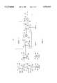
- FIG. 1is a block diagram of a logic module according to a presently preferred embodiment of the present invention.
- FIG. 2ais a diagram showing a combinatorial circuit for generating the CLEAR, HOLD1, and HOLD2 signals for the circuit of FIG. 1 from data inputs.
- FIG. 2bis a logic diagram in block form of a presently preferred circuit for use in performing the function of the circuit of FIG. 2a.
- FIG. 3is a diagram showing a logic module according to a presently preferred embodiment of the invention wherein the portions of the logic module shown in FIGS. 1 and 2b have been combined.
- FIG. 4is an equivalent simplified diagram of a first illustrative embodiment of the circuit of FIG. 3 wherein the sequential portion of the logic module has been configured as a flip-flop.
- FIG. 5is an equivalent simplified diagram of a second illustrative embodiment of the circuit of FIG. 3 wherein the sequential portion of the logic module has been configured as a latch.
- a logic module 10having configurable combinational and sequential blocks.
- the combinatorial portion of the logic moduleincludes first and second sections.
- a first section of the logic module 10 of the present inventionincludes first and second two-input multiplexers 12 and 14.
- First two-input multiplexerincludes first and second data inputs 16 and 18, select input 20 and output 22.
- Second two-input multiplexerhas first and second data inputs 24 and 26, select input 28 and output 30. Select inputs 20 and 28 of first and second two-input multiplexers 12 and 14 are connected to the output 32 of a two-input logic gate of a first type 34 having first and second data inputs 50 and 54.
- Outputs 22 and 30 of first and second two-input multiplexers 12 and 14are connected to data inputs 36 and 38 of third two-input multiplexer 40, in a second section of logic module 10.
- Third two-input multiplexer 40also includes select input 42 and output 44. Select input 42 of third two-input multiplexer 40 is connected to output 46 of a two-input logic gate of a second type 48 having first and second data inputs 52 and 56.
- the data inputs 16, 18, 24 and 26 to the first and second two-input multiplexersare sourced with data signals from a first group of data input nodes shown in FIG. 1 as data inputs D00, D01, D10, and D11.
- One input of each of logic gates 34 and 48(reference numerals 50 and 52, respectively) is sourced from a data signal of a second group shown in FIG. 1 as data input nodes A0 and A1, respectively, and the other input of each of the logic gates (reference numerals 54 and 56, respectively) is sourced from a data signal of a third group shown in FIG. 1 as data input nodes B0 and B1, respectively.
- the logic module 10 of the present inventionoffers a plurality of combinatorial functions having up to eight inputs.
- the function implemented by the circuit of FIG. 1is:
- the combinatorial functions which may be implementedinclude AND, OR, NAND, NOR, and EX-OR. TABLE I shows the implementation of these functions using different inputs of the circuit of FIG. 1.
- the sequential portion of logic module 10also has two stages.
- the output 44 of the third two-input multiplexer 40is connected to a first data input 58 of a fourth two-input multiplexer 60 having its select input 62 driven by a HOLD1 signal from a HOLD1 control node.
- Its output 64 and a CLEAR signal from a CLEAR control nodeare presented to inputs 66 and 68 of an AND gate 70 whose output 72 is connected to the second data input 74 of the fourth two-input multiplexer and to the first data input 76 of a fifth two-input multiplexer 78, which forms the input to the second sequential stage.
- the select input 80 of the fifth two-input multiplexer 78is connected to a HOLD2 signal from a HOLD2 control node.
- Output 82 of fifth two-input multiplexer 78 and the CLEAR signalare presented to inputs 84 and 86 of an AND gate 88 whose output 90 is connected to the second data input 92 of the fifth two-input multiplexer and to an output node 94.
- the CLEAR, HOLD1 and HOLD2 signalsare derived by combinatorial logic from a set of data input signals. As is shown in FIG. 2a, data signals from data input nodes C1, C2 and B0 are presented to inputs 96, 98, and 100, respectively of logic combining circuit 102, which has control node outputs upon which the HOLD1, HOLD2, and CLEAR signals appear, respectively.
- the logic combining circuit 102 of FIG. 2amay be any logic circuit for combining the three inputs in a manner which produces outputs for the HOLD1, HOLD2, and CLEAR signals as set forth in the truth table in TABLE II.
- FIG. 2bis a logic diagram of a presently preferred embodiment of such a circuit.
- logic combining circuit 102includes AND gate 104 with inverting input 106 and non-inverting input 108, and output 110, AND gate 112 with inverting input 114 and noninverting input 116 and output 118, EXNOR gate 120 with inputs 122 and 124 and output 126 and OR gate 128 with inputs 130 and 132 and output 134.
- C1 input 96is connected to inputs 106 and 116 of AND gates 104 and 112, respectively and to input 122 of EXNOR gate 120.
- C2 input 98is connected to inputs 108 and 114 of AND gates 104 and 112, respectively, and to input 124 of EXNOR gate 120.
- B0 input 100is connected to input 132 of OR gate 128.
- the output 112 of AND gate 112is connected to input 130 of OR gate 128.
- the output 110 of AND gate 104is the HOLD1 signal
- the output 126 of EXNOR gate 120is the HOLD2 signal
- the output 134 of OR gate 128is the clear signal.
- the sequential portion of the logic module of the present invention disclosed hereinis configurable as a rising or falling edge flip flop with asynchronous low active clear, a transparent low or high latch with asynchronous low active clear, or as a transparent flow-through element which allows only the combinatorial section of the module to be used. All latches and flip flops are non-inverting.
- TABLE IIIillustrates the sequential functions available from the logic module of the present invention. From TABLE III, it can be seen that the sequential functions which may be performed include a negative triggered latch with low active clear, a positive triggered latch with low active clear, a negative triggered flip flop with low active clear, a positive triggered flip flop with low active clear and a flow through mode.
- the states of inputs A0, D00 and D10are restricted for positive and negative triggered latches. A0 must equal 1 and both D00 and D10 must equal 0 in order for the output to be low when the latch is in transparent mode and the clear input is active.
- the two-input multiplexers and other logic components of the logic module of the present inventionmay be fabricated using conventional MOS and CMOS technology.
- module 10may be configured to include a rising edge flip flop as the sequential element by placing a logic zero at input C1, using input C2 as a clock, and using input B0 as a low-active clear input.
- the sequential portion of module 10may be configured as a high-logic or low-logic triggered latch as described in Table III.
- flip-flop 140includes a data input 142 connected to output 44 of third multiplexer 40.
- Flip-flop 140includes a data input 142 connected to output 44 of third multiplexer 40.
- Flip-flop 140also includes Q output 144, clock (CLK) input 146, and low-active clear (
- CLKclock
- CLRlow-active clear
- module 10may be configured to include a high or low logic triggered latch as the sequential element by placing a logic one at input C1, using input C2 as a clock, and using input B0 as a low-active clear input.
- Latch 150includes a data input 152 connected to output 44 of third multiplexer 40.
- Latch 150also includes Q output 154, latch input 156, and low-active clear (
Landscapes
- Physics & Mathematics (AREA)
- Engineering & Computer Science (AREA)
- Computer Hardware Design (AREA)
- Computing Systems (AREA)
- General Engineering & Computer Science (AREA)
- Mathematical Physics (AREA)
- Logic Circuits (AREA)
Abstract
Description
Z=(D00|(A0·B0)+D01 (A0·B0))|(A1+B1)+(D10|(A0·B0)+D11(A0 B0)) (A1+B1)
TABLE I ______________________________________ FUNCTION A0 B0 A1 B1 D00 D01 D10 D11 C1 C2 ______________________________________NAND A B 1X X X 1 0 1 0 |(A · B)A B X 1X X 1 0 1 0A B 0 0 1 0X X 1 0A B 0 0 1 0 0 0 1 0 1 A 0B 1 1 1 0 1 0 1A B 0 1 1 1 0 1 0 A 1 0B 1 1 1 0 1 0 A 1B 0 1 1 1 0 1 0 NOR |(A +B) 1 1 A B X 1X 0 1 0 0 X A B X X 0X 1 0X 0 A B X X 0X i 0 1 A 0B 1 0 0 0 1 0 1A B 0 1 0 0 0 1 0 A 1 0B 1 0 0 0 1 0 A 1B 0 1 0 0 0 1 0 AND (A · B)A B 0 0 0 1X X 1 0A B 1X X X 0 1 1 0A B X 1X X 0 1 1 0A B 0 0 0 0 1 0 1 0 1A B 0 0 0 0 1 1 0 1 A 0B 0 0 0 0 1 0 A 1B 0 0 0 0 1 1 0 A 1 0B 0 0 0 1 1 0 OR (A +B) X X A B 0 0 1 1 1 0 0 X A B 0 X 1X 1 0X 0 A B 0 X 1X 1 0 1 A 0B 0 1 1 1 1 0 1A B 0 0 1 1 1 1 0 A 1 0B 0 1 1 1 1 0 A 1B 0 0 1 1 1 1 0 XOR A 1B 0 0 1 1 0 1 0 (A · |B) + A 1 0B 0 1 1 0 1 0 (|A ·B) 1A B 0 0 1 1 0 1 0 1 A 0B 0 1 1 0 1 0 XNOR A 1B 0 1 0 0 1 1 0 (A · B) + A 1 0B 1 0 0 1 1 0 (|A · |B) 1A B 0 1 0 0 1 1 0 1 A 0B 1 0 0 1 1 0 ______________________________________
TABLE II ______________________________________ C1 C2 HOLD1 HOLD2 CLRB ______________________________________ 0 0 0 1B0 0 1 1 0B0 1 0 0 0 1 1 1 0 1 B0 ______________________________________
TABLE III ______________________________________ C1 C2 FUNCTION |CLEAR RESTRICTIONS ______________________________________ 0 CLK Rising Edge Flip FlopB0 None CLK 1 Falling Edge FlipFlop B0 None 1 CLK High Latch with Clear B0 A0 = 1; D00, D10 = 0CLK 0 Low Latch with Clear B0 A0 = 1; D00, D10 = 0 1 CLK High Latch -- B0 = 1CLK 0 Low latch -- B0 = 1 1 0 Transparent -- None ______________________________________
Claims (13)
Priority Applications (1)
| Application Number | Priority Date | Filing Date | Title |
|---|---|---|---|
| US08/754,188US5781033A (en) | 1990-05-11 | 1996-11-12 | Logic module with configurable combinational and sequential blocks |
Applications Claiming Priority (5)
| Application Number | Priority Date | Filing Date | Title |
|---|---|---|---|
| US07/522,232US5055718A (en) | 1990-05-11 | 1990-05-11 | Logic module with configurable combinational and sequential blocks |
| US07/773,353US5198705A (en) | 1990-05-11 | 1991-10-07 | Logic module with configurable combinational and sequential blocks |
| US08/028,789US5440245A (en) | 1990-05-11 | 1993-03-09 | Logic module with configurable combinational and sequential blocks |
| US08/505,830US5610534A (en) | 1990-05-11 | 1995-05-18 | Logic module for a programmable logic device |
| US08/754,188US5781033A (en) | 1990-05-11 | 1996-11-12 | Logic module with configurable combinational and sequential blocks |
Related Parent Applications (1)
| Application Number | Title | Priority Date | Filing Date |
|---|---|---|---|
| US08/505,830ContinuationUS5610534A (en) | 1990-05-11 | 1995-05-18 | Logic module for a programmable logic device |
Publications (1)
| Publication Number | Publication Date |
|---|---|
| US5781033Atrue US5781033A (en) | 1998-07-14 |
Family
ID=27060751
Family Applications (4)
| Application Number | Title | Priority Date | Filing Date |
|---|---|---|---|
| US07/773,353Expired - LifetimeUS5198705A (en) | 1990-05-11 | 1991-10-07 | Logic module with configurable combinational and sequential blocks |
| US08/028,789Expired - LifetimeUS5440245A (en) | 1990-05-11 | 1993-03-09 | Logic module with configurable combinational and sequential blocks |
| US08/505,830Expired - LifetimeUS5610534A (en) | 1990-05-11 | 1995-05-18 | Logic module for a programmable logic device |
| US08/754,188Expired - LifetimeUS5781033A (en) | 1990-05-11 | 1996-11-12 | Logic module with configurable combinational and sequential blocks |
Family Applications Before (3)
| Application Number | Title | Priority Date | Filing Date |
|---|---|---|---|
| US07/773,353Expired - LifetimeUS5198705A (en) | 1990-05-11 | 1991-10-07 | Logic module with configurable combinational and sequential blocks |
| US08/028,789Expired - LifetimeUS5440245A (en) | 1990-05-11 | 1993-03-09 | Logic module with configurable combinational and sequential blocks |
| US08/505,830Expired - LifetimeUS5610534A (en) | 1990-05-11 | 1995-05-18 | Logic module for a programmable logic device |
Country Status (1)
| Country | Link |
|---|---|
| US (4) | US5198705A (en) |
Cited By (11)
| Publication number | Priority date | Publication date | Assignee | Title |
|---|---|---|---|---|
| US5977792A (en)* | 1997-12-15 | 1999-11-02 | Texas Instruments Incorporated | Configurable logic circuit and method |
| US6236229B1 (en) | 1999-05-13 | 2001-05-22 | Easic Corporation | Integrated circuits which employ look up tables to provide highly efficient logic cells and logic functionalities |
| US6245634B1 (en) | 1999-10-28 | 2001-06-12 | Easic Corporation | Method for design and manufacture of semiconductors |
| US6323690B1 (en)* | 1997-11-28 | 2001-11-27 | Hitachi, Ltd. | Logic circuit and its forming method |
| US6331733B1 (en) | 1999-08-10 | 2001-12-18 | Easic Corporation | Semiconductor device |
| US6331790B1 (en) | 2000-03-10 | 2001-12-18 | Easic Corporation | Customizable and programmable cell array |
| US6480054B2 (en)* | 2000-01-04 | 2002-11-12 | Dzung Joseph Tran | Digital electronic circuit for use in implementing digital logic functions |
| US6756811B2 (en) | 2000-03-10 | 2004-06-29 | Easic Corporation | Customizable and programmable cell array |
| US20160373091A1 (en)* | 2015-06-16 | 2016-12-22 | The Athena Group, Inc. | Minimizing information leakage from combinatorial logic |
| US11671099B2 (en) | 2021-05-21 | 2023-06-06 | Microchip Technology Inc. | Logic cell for programmable gate array |
| US12223322B2 (en) | 2021-10-07 | 2025-02-11 | Microchip Technology Inc. | Embedded processor supporting fixed-function kernels |
Families Citing this family (122)
| Publication number | Priority date | Publication date | Assignee | Title |
|---|---|---|---|---|
| US5451887A (en) | 1986-09-19 | 1995-09-19 | Actel Corporation | Programmable logic module and architecture for field programmable gate array device |
| US5477165A (en)* | 1986-09-19 | 1995-12-19 | Actel Corporation | Programmable logic module and architecture for field programmable gate array device |
| US5198705A (en) | 1990-05-11 | 1993-03-30 | Actel Corporation | Logic module with configurable combinational and sequential blocks |
| US5661661A (en)* | 1990-12-21 | 1997-08-26 | Synopsys, Inc. | Method for processing a hardware independent user description to generate logic circuit elements including flip-flops, latches, and three-state buffers and combinations thereof |
| US5268598A (en)* | 1991-04-25 | 1993-12-07 | Altera Corporation | High-density erasable programmable logic device architecture using multiplexer interconnections |
| US5384499A (en)* | 1991-04-25 | 1995-01-24 | Altera Corporation | High-density erasable programmable logic device architecture using multiplexer interconnections |
| US5646547A (en)* | 1994-04-28 | 1997-07-08 | Xilinx, Inc. | Logic cell which can be configured as a latch without static one's problem |
| US5365125A (en)* | 1992-07-23 | 1994-11-15 | Xilinx, Inc. | Logic cell for field programmable gate array having optional internal feedback and optional cascade |
| US5302866A (en)* | 1993-03-18 | 1994-04-12 | Xilinx, Inc. | Input circuit block and method for PLDs with register clock enable selection |
| US5546018A (en)* | 1993-09-02 | 1996-08-13 | Xilinx, Inc. | Fast carry structure with synchronous input |
| US5481206A (en)* | 1993-09-02 | 1996-01-02 | Xilinx, Inc. | Circuit for fast carry and logic |
| US6154053A (en)* | 1993-09-02 | 2000-11-28 | Xilinx, Inc. | Look-ahead carry structure with homogeneous CLB structure and pitch larger than CLB pitch |
| US5629886A (en)* | 1993-09-02 | 1997-05-13 | Xilinx, Inc. | Method and structure for providing fast propagation of a carry signal in a field programmable gate array |
| US6288570B1 (en) | 1993-09-02 | 2001-09-11 | Xilinx, Inc. | Logic structure and circuit for fast carry |
| US5898319A (en)* | 1993-09-02 | 1999-04-27 | Xilinx, Inc. | Method and structure for providing fast conditional sum in a field programmable gate array |
| US5349250A (en)* | 1993-09-02 | 1994-09-20 | Xilinx, Inc. | Logic structure and circuit for fast carry |
| USRE38451E1 (en)* | 1993-11-12 | 2004-03-02 | Altera Corporation | Universal logic module with arithmetic capabilities |
| US5436574A (en)* | 1993-11-12 | 1995-07-25 | Altera Corporation | Universal logic module with arithmetic capabilities |
| US5581200A (en)* | 1994-03-04 | 1996-12-03 | Gudger; Keith H. | Stored and combinational logic function generator without dedicated storage elements |
| US5781756A (en)* | 1994-04-01 | 1998-07-14 | Xilinx, Inc. | Programmable logic device with partially configurable memory cells and a method for configuration |
| US5504439A (en)* | 1994-04-01 | 1996-04-02 | Xilinx, Inc. | I/O interface cell for use with optional pad |
| US5430687A (en)* | 1994-04-01 | 1995-07-04 | Xilinx, Inc. | Programmable logic device including a parallel input device for loading memory cells |
| US5682107A (en)* | 1994-04-01 | 1997-10-28 | Xilinx, Inc. | FPGA architecture with repeatable tiles including routing matrices and logic matrices |
| US5453706A (en)* | 1994-04-01 | 1995-09-26 | Xilinx, Inc. | Field programmable gate array providing contention free configuration and reconfiguration |
| US5550843A (en)* | 1994-04-01 | 1996-08-27 | Xilinx, Inc. | Programmable scan chain testing structure and method |
| IL109491A (en)* | 1994-05-01 | 1999-11-30 | Quick Tech Ltd | Customizable logic array device |
| WO1995030952A1 (en)* | 1994-05-04 | 1995-11-16 | Atmel Corporation | Programmable logic device with regional and universal signal routing |
| US5424655A (en)* | 1994-05-20 | 1995-06-13 | Quicklogic Corporation | Programmable application specific integrated circuit employing antifuses and methods therefor |
| KR960003103A (en)* | 1994-06-30 | 1996-01-26 | 윌리엄 이. 힐러 | Association Heterogenius Field Programmable Gate Array Logic Module and Formation Method thereof |
| US5491431A (en)* | 1994-10-05 | 1996-02-13 | Texas Instruments Incorporated | Logic module core cell for gate arrays |
| US5450022A (en)* | 1994-10-07 | 1995-09-12 | Xilinx Inc. | Structure and method for configuration of a field programmable gate array |
| FR2726409B1 (en)* | 1994-10-28 | 1996-12-13 | Suisse Electronique Microtech | MULTIPLEXER OF LOGIC VARIABLES |
| US5495181A (en)* | 1994-12-01 | 1996-02-27 | Quicklogic Corporation | Integrated circuit facilitating simultaneous programming of multiple antifuses |
| US5552720A (en)* | 1994-12-01 | 1996-09-03 | Quicklogic Corporation | Method for simultaneous programming of multiple antifuses |
| US5635857A (en)* | 1994-12-08 | 1997-06-03 | Unisys Corporation | IC chip using a common multiplexor logic element for performing logic operations |
| US5508637A (en)* | 1995-01-05 | 1996-04-16 | Texas Instruments Incorporated | Logic module for a field programmable gate array |
| US6028446A (en)* | 1995-06-06 | 2000-02-22 | Advanced Micro Devices, Inc. | Flexible synchronous and asynchronous circuits for a very high density programmable logic device |
| US6053948A (en)* | 1995-06-07 | 2000-04-25 | Synopsys, Inc. | Method and apparatus using a memory model |
| US5784593A (en)* | 1995-09-29 | 1998-07-21 | Synopsys, Inc. | Simulator including process levelization |
| US5809283A (en)* | 1995-09-29 | 1998-09-15 | Synopsys, Inc. | Simulator for simulating systems including mixed triggers |
| US5943242A (en) | 1995-11-17 | 1999-08-24 | Pact Gmbh | Dynamically reconfigurable data processing system |
| US7266725B2 (en) | 2001-09-03 | 2007-09-04 | Pact Xpp Technologies Ag | Method for debugging reconfigurable architectures |
| US5760611A (en)* | 1996-10-25 | 1998-06-02 | International Business Machines Corporation | Function generator for programmable gate array |
| DE19651075A1 (en) | 1996-12-09 | 1998-06-10 | Pact Inf Tech Gmbh | Unit for processing numerical and logical operations, for use in processors (CPU's), multi-computer systems, data flow processors (DFP's), digital signal processors (DSP's) or the like |
| DE19654595A1 (en) | 1996-12-20 | 1998-07-02 | Pact Inf Tech Gmbh | I0 and memory bus system for DFPs as well as building blocks with two- or multi-dimensional programmable cell structures |
| US6338106B1 (en) | 1996-12-20 | 2002-01-08 | Pact Gmbh | I/O and memory bus system for DFPS and units with two or multi-dimensional programmable cell architectures |
| DE19654593A1 (en) | 1996-12-20 | 1998-07-02 | Pact Inf Tech Gmbh | Reconfiguration procedure for programmable blocks at runtime |
| DE19654846A1 (en)* | 1996-12-27 | 1998-07-09 | Pact Inf Tech Gmbh | Process for the independent dynamic reloading of data flow processors (DFPs) as well as modules with two- or multi-dimensional programmable cell structures (FPGAs, DPGAs, etc.) |
| ATE243390T1 (en) | 1996-12-27 | 2003-07-15 | Pact Inf Tech Gmbh | METHOD FOR INDEPENDENT DYNAMIC LOADING OF DATA FLOW PROCESSORS (DFPS) AND COMPONENTS WITH TWO- OR MULTI-DIMENSIONAL PROGRAMMABLE CELL STRUCTURES (FPGAS, DPGAS, O.L.) |
| US5936426A (en) | 1997-02-03 | 1999-08-10 | Actel Corporation | Logic function module for field programmable array |
| DE19704044A1 (en)* | 1997-02-04 | 1998-08-13 | Pact Inf Tech Gmbh | Address generation with systems having programmable modules |
| US6542998B1 (en) | 1997-02-08 | 2003-04-01 | Pact Gmbh | Method of self-synchronization of configurable elements of a programmable module |
| DE19704728A1 (en) | 1997-02-08 | 1998-08-13 | Pact Inf Tech Gmbh | Method for self-synchronization of configurable elements of a programmable module |
| DE19704742A1 (en) | 1997-02-11 | 1998-09-24 | Pact Inf Tech Gmbh | Internal bus system for DFPs, as well as modules with two- or multi-dimensional programmable cell structures, for coping with large amounts of data with high networking effort |
| US5889411A (en)* | 1997-02-26 | 1999-03-30 | Xilinx, Inc. | FPGA having logic element carry chains capable of generating wide XOR functions |
| US6201410B1 (en) | 1997-02-26 | 2001-03-13 | Xilinx, Inc. | Wide logic gate implemented in an FPGA configurable logic element |
| US5914616A (en)* | 1997-02-26 | 1999-06-22 | Xilinx, Inc. | FPGA repeatable interconnect structure with hierarchical interconnect lines |
| US5942913A (en)* | 1997-03-20 | 1999-08-24 | Xilinx, Inc. | FPGA repeatable interconnect structure with bidirectional and unidirectional interconnect lines |
| US5963050A (en)* | 1997-02-26 | 1999-10-05 | Xilinx, Inc. | Configurable logic element with fast feedback paths |
| US6204689B1 (en) | 1997-02-26 | 2001-03-20 | Xilinx, Inc. | Input/output interconnect circuit for FPGAs |
| US5920202A (en)* | 1997-02-26 | 1999-07-06 | Xilinx, Inc. | Configurable logic element with ability to evaluate five and six input functions |
| US6150837A (en)* | 1997-02-28 | 2000-11-21 | Actel Corporation | Enhanced field programmable gate array |
| US6014038A (en)* | 1997-03-21 | 2000-01-11 | Lightspeed Semiconductor Corporation | Function block architecture for gate array |
| US8686549B2 (en) | 2001-09-03 | 2014-04-01 | Martin Vorbach | Reconfigurable elements |
| DE19861088A1 (en) | 1997-12-22 | 2000-02-10 | Pact Inf Tech Gmbh | Repairing integrated circuits by replacing subassemblies with substitutes |
| DE19807872A1 (en) | 1998-02-25 | 1999-08-26 | Pact Inf Tech Gmbh | Method of managing configuration data in data flow processors |
| US6038627A (en)* | 1998-03-16 | 2000-03-14 | Actel Corporation | SRAM bus architecture and interconnect to an FPGA |
| US6049487A (en)* | 1998-03-16 | 2000-04-11 | Actel Corporation | Embedded static random access memory for field programmable gate array |
| US6237124B1 (en)* | 1998-03-16 | 2001-05-22 | Actel Corporation | Methods for errors checking the configuration SRAM and user assignable SRAM data in a field programmable gate array |
| US6772387B1 (en)* | 1998-03-16 | 2004-08-03 | Actel Corporation | Cyclic redundancy checking of a field programmable gate array having an SRAM memory architecture |
| US7389487B1 (en) | 1998-04-28 | 2008-06-17 | Actel Corporation | Dedicated interface architecture for a hybrid integrated circuit |
| US6549035B1 (en) | 1998-09-15 | 2003-04-15 | Actel Corporation | High density antifuse based partitioned FPGA architecture |
| JP3665231B2 (en) | 1999-06-03 | 2005-06-29 | 株式会社ルネサステクノロジ | Logic circuit |
| WO2000077652A2 (en) | 1999-06-10 | 2000-12-21 | Pact Informationstechnologie Gmbh | Sequence partitioning in cell structures |
| US6822976B1 (en)* | 1999-11-03 | 2004-11-23 | Intel Corporation | Method and apparatus for high throughput multiplexing of data |
| JP3472527B2 (en) | 2000-05-16 | 2003-12-02 | 松下電器産業株式会社 | Logic circuit module, semiconductor integrated circuit design method using the same, and semiconductor integrated circuit |
| EP2226732A3 (en) | 2000-06-13 | 2016-04-06 | PACT XPP Technologies AG | Cache hierarchy for a multicore processor |
| US8058899B2 (en) | 2000-10-06 | 2011-11-15 | Martin Vorbach | Logic cell array and bus system |
| AU2060002A (en) | 2000-10-06 | 2002-04-22 | Pact Inf Tech Gmbh | Method and device |
| US6990555B2 (en)* | 2001-01-09 | 2006-01-24 | Pact Xpp Technologies Ag | Method of hierarchical caching of configuration data having dataflow processors and modules having two- or multidimensional programmable cell structure (FPGAs, DPGAs, etc.) |
| US7444531B2 (en) | 2001-03-05 | 2008-10-28 | Pact Xpp Technologies Ag | Methods and devices for treating and processing data |
| US7844796B2 (en) | 2001-03-05 | 2010-11-30 | Martin Vorbach | Data processing device and method |
| US7210129B2 (en) | 2001-08-16 | 2007-04-24 | Pact Xpp Technologies Ag | Method for translating programs for reconfigurable architectures |
| US7581076B2 (en) | 2001-03-05 | 2009-08-25 | Pact Xpp Technologies Ag | Methods and devices for treating and/or processing data |
| US9037807B2 (en) | 2001-03-05 | 2015-05-19 | Pact Xpp Technologies Ag | Processor arrangement on a chip including data processing, memory, and interface elements |
| AU2002347560A1 (en)* | 2001-06-20 | 2003-01-02 | Pact Xpp Technologies Ag | Data processing method |
| US7996827B2 (en) | 2001-08-16 | 2011-08-09 | Martin Vorbach | Method for the translation of programs for reconfigurable architectures |
| US7434191B2 (en) | 2001-09-03 | 2008-10-07 | Pact Xpp Technologies Ag | Router |
| US8686475B2 (en) | 2001-09-19 | 2014-04-01 | Pact Xpp Technologies Ag | Reconfigurable elements |
| US7577822B2 (en) | 2001-12-14 | 2009-08-18 | Pact Xpp Technologies Ag | Parallel task operation in processor and reconfigurable coprocessor configured based on information in link list including termination information for synchronization |
| DE10392560D2 (en) | 2002-01-19 | 2005-05-12 | Pact Xpp Technologies Ag | Reconfigurable processor |
| US8127061B2 (en) | 2002-02-18 | 2012-02-28 | Martin Vorbach | Bus systems and reconfiguration methods |
| US8914590B2 (en) | 2002-08-07 | 2014-12-16 | Pact Xpp Technologies Ag | Data processing method and device |
| US6774667B1 (en) | 2002-05-09 | 2004-08-10 | Actel Corporation | Method and apparatus for a flexible chargepump scheme for field-programmable gate arrays |
| US7378867B1 (en) | 2002-06-04 | 2008-05-27 | Actel Corporation | Field-programmable gate array low voltage differential signaling driver utilizing two complimentary output buffers |
| US6891394B1 (en) | 2002-06-04 | 2005-05-10 | Actel Corporation | Field-programmable gate array low voltage differential signaling driver utilizing two complimentary output buffers |
| AU2003286131A1 (en) | 2002-08-07 | 2004-03-19 | Pact Xpp Technologies Ag | Method and device for processing data |
| US7657861B2 (en) | 2002-08-07 | 2010-02-02 | Pact Xpp Technologies Ag | Method and device for processing data |
| US6765427B1 (en) | 2002-08-08 | 2004-07-20 | Actel Corporation | Method and apparatus for bootstrapping a programmable antifuse circuit |
| US7434080B1 (en) | 2002-09-03 | 2008-10-07 | Actel Corporation | Apparatus for interfacing and testing a phase locked loop in a field programmable gate array |
| US7394284B2 (en) | 2002-09-06 | 2008-07-01 | Pact Xpp Technologies Ag | Reconfigurable sequencer structure |
| US6750674B1 (en) | 2002-10-02 | 2004-06-15 | Actel Corporation | Carry chain for use between logic modules in a field programmable gate array |
| US6885218B1 (en) | 2002-10-08 | 2005-04-26 | Actel Corporation | Parallel programmable antifuse field programmable gate array device (FPGA) and a method for programming and testing an antifuse FPGA |
| US7269814B1 (en) | 2002-10-08 | 2007-09-11 | Actel Corporation | Parallel programmable antifuse field programmable gate array device (FPGA) and a method for programming and testing an antifuse FPGA |
| US6727726B1 (en) | 2002-11-12 | 2004-04-27 | Actel Corporation | Field programmable gate array architecture including a buffer module and a method of distributing buffer modules in a field programmable gate array |
| US6946871B1 (en) | 2002-12-18 | 2005-09-20 | Actel Corporation | Multi-level routing architecture in a field programmable gate array having transmitters and receivers |
| US6891396B1 (en) | 2002-12-27 | 2005-05-10 | Actel Corporation | Repeatable block producing a non-uniform routing architecture in a field programmable gate array having segmented tracks |
| US7385420B1 (en) | 2002-12-27 | 2008-06-10 | Actel Corporation | Repeatable block producing a non-uniform routing architecture in a field programmable gate array having segmented tracks |
| US7375553B1 (en) | 2003-05-28 | 2008-05-20 | Actel Corporation | Clock tree network in a field programmable gate array |
| US6838902B1 (en)* | 2003-05-28 | 2005-01-04 | Actel Corporation | Synchronous first-in/first-out block memory for a field programmable gate array |
| US6825690B1 (en) | 2003-05-28 | 2004-11-30 | Actel Corporation | Clock tree network in a field programmable gate array |
| US6867615B1 (en) | 2003-05-30 | 2005-03-15 | Actel Corporation | Dedicated input/output first in/first out module for a field programmable gate array |
| US7385419B1 (en)* | 2003-05-30 | 2008-06-10 | Actel Corporation | Dedicated input/output first in/first out module for a field programmable gate array |
| US6867617B2 (en)* | 2003-07-18 | 2005-03-15 | Agere Systems Inc. | Half-rate clock logic block and method for forming same |
| EP1676208A2 (en) | 2003-08-28 | 2006-07-05 | PACT XPP Technologies AG | Data processing device and method |
| JP2009524134A (en) | 2006-01-18 | 2009-06-25 | ペーアーツェーテー イクスペーペー テクノロジーズ アクチエンゲゼルシャフト | Hardware definition method |
| FR2933826B1 (en)* | 2008-07-09 | 2011-11-18 | Univ Paris Curie | PROGRAMMABLE LOGIC NETWORK, INTERCONNECT SWITCH AND LOGIC UNIT FOR SUCH A NETWORK |
| US8719648B2 (en) | 2011-07-27 | 2014-05-06 | International Business Machines Corporation | Interleaving of memory repair data compression and fuse programming operations in single fusebay architecture |
| US8467260B2 (en) | 2011-08-05 | 2013-06-18 | International Business Machines Corporation | Structure and method for storing multiple repair pass data into a fusebay |
| US8484543B2 (en) | 2011-08-08 | 2013-07-09 | International Business Machines Corporation | Fusebay controller structure, system, and method |
| US8537627B2 (en) | 2011-09-01 | 2013-09-17 | International Business Machines Corporation | Determining fusebay storage element usage |
| US8912824B1 (en)* | 2013-09-05 | 2014-12-16 | International Business Machines Corporation | Method and apparatus for detecting rising and falling transitions of internal signals of an integrated circuit |
Citations (156)
| Publication number | Priority date | Publication date | Assignee | Title |
|---|---|---|---|---|
| US3106698A (en)* | 1958-04-25 | 1963-10-08 | Bell Telephone Labor Inc | Parallel data processing apparatus |
| US3184603A (en)* | 1961-02-23 | 1965-05-18 | Ibm | Logic performing device |
| US3201574A (en)* | 1960-10-07 | 1965-08-17 | Rca Corp | Flexible logic circuit |
| US3287703A (en)* | 1962-12-04 | 1966-11-22 | Westinghouse Electric Corp | Computer |
| US3287702A (en)* | 1962-12-04 | 1966-11-22 | Westinghouse Electric Corp | Computer control |
| GB1101851A (en) | 1965-01-20 | 1968-01-31 | Ncr Co | Generalized logic circuitry |
| US3381117A (en)* | 1965-08-02 | 1968-04-30 | Ibm | Minimal pin multipurpose logic circuits |
| US3423646A (en)* | 1965-02-01 | 1969-01-21 | Sperry Rand Corp | Computer logic device consisting of an array of tunneling diodes,isolators and short circuits |
| US3428903A (en)* | 1965-08-02 | 1969-02-18 | Ibm | Multipurpose logic circuit for performing 254 out of 256 discrete logical combinations of three variables |
| US3439185A (en)* | 1966-01-11 | 1969-04-15 | Rca Corp | Logic circuits employing field-effect transistors |
| US3473160A (en)* | 1966-10-10 | 1969-10-14 | Stanford Research Inst | Electronically controlled microelectronic cellular logic array |
| US3564514A (en)* | 1969-05-23 | 1971-02-16 | Honeywell Inc | Programmable logic apparatus |
| US3576984A (en)* | 1968-08-09 | 1971-05-04 | Bunker Ramo | Multifunction logic network |
| US3619583A (en)* | 1968-10-11 | 1971-11-09 | Bell Telephone Labor Inc | Multiple function programmable arrays |
| US3731073A (en)* | 1972-04-05 | 1973-05-01 | Bell Telephone Labor Inc | Programmable switching array |
| US3750115A (en)* | 1972-04-28 | 1973-07-31 | Gen Electric | Read mostly associative memory cell for universal logic |
| US3806891A (en)* | 1972-12-26 | 1974-04-23 | Ibm | Logic circuit for scan-in/scan-out |
| US3816725A (en)* | 1972-04-28 | 1974-06-11 | Gen Electric | Multiple level associative logic circuits |
| US3818252A (en)* | 1971-12-20 | 1974-06-18 | Hitachi Ltd | Universal logical integrated circuit |
| US3818452A (en)* | 1972-04-28 | 1974-06-18 | Gen Electric | Electrically programmable logic circuits |
| US3838296A (en)* | 1973-10-29 | 1974-09-24 | Nat Semiconductor Corp | Emitter coupled logic transistor circuit |
| US3849638A (en)* | 1973-07-18 | 1974-11-19 | Gen Electric | Segmented associative logic circuits |
| US3902050A (en)* | 1973-04-26 | 1975-08-26 | Siemens Ag | Serial programmable combinational switching function generator |
| US3912914A (en)* | 1972-12-26 | 1975-10-14 | Bell Telephone Labor Inc | Programmable switching array |
| US4032894A (en)* | 1976-06-01 | 1977-06-28 | International Business Machines Corporation | Logic array with enhanced flexibility |
| US4091359A (en)* | 1976-02-20 | 1978-05-23 | Siemens Aktiengesellschaft | Modular logic circuit utilizing charge-storage transistors |
| US4140924A (en)* | 1975-12-10 | 1979-02-20 | Centre Electronique Horloger S.A. | Logic CMOS transistor circuits |
| US4153938A (en)* | 1977-08-18 | 1979-05-08 | Monolithic Memories Inc. | High speed combinatorial digital multiplier |
| US4157589A (en)* | 1977-09-09 | 1979-06-05 | Gte Laboratories Incorporated | Arithmetic logic apparatus |
| US4157480A (en)* | 1976-08-03 | 1979-06-05 | National Research Development Corporation | Inverters and logic gates employing inverters |
| US4195352A (en)* | 1977-07-08 | 1980-03-25 | Xerox Corporation | Split programmable logic array |
| US4240094A (en)* | 1978-03-20 | 1980-12-16 | Harris Corporation | Laser-configured logic array |
| US4293783A (en)* | 1978-11-01 | 1981-10-06 | Massachusetts Institute Of Technology | Storage/logic array |
| US4354266A (en)* | 1979-10-31 | 1982-10-12 | Gte Laboratories Incorporated | Multiplexor with decoding |
| US4354228A (en)* | 1979-12-20 | 1982-10-12 | International Business Machines Corporation | Flexible processor on a single semiconductor substrate using a plurality of arrays |
| GB2045488B (en) | 1979-01-16 | 1982-10-13 | Nippon Telegraph & Telephone | Programmable sequential logic circuit devices |
| US4357678A (en)* | 1979-12-26 | 1982-11-02 | International Business Machines Corporation | Programmable sequential logic array mechanism |
| US4409499A (en)* | 1982-06-14 | 1983-10-11 | Standard Microsystems Corporation | High-speed merged plane logic function array |
| US4414547A (en)* | 1981-08-05 | 1983-11-08 | General Instrument Corporation | Storage logic array having two conductor data column |
| US4424456A (en)* | 1979-12-26 | 1984-01-03 | Tokyo Shibaura Denki Kabushiki Kaisha | Driver circuit for charge coupled device |
| US4453096A (en)* | 1976-11-04 | 1984-06-05 | U.S. Philips Corporation | MOS Transistor type integrated circuit for the execution of logical operations on a plurality of data signals |
| US4491839A (en)* | 1981-05-21 | 1985-01-01 | Itt Industries, Inc. | CMOS Selection circuit |
| US4513307A (en)* | 1982-05-05 | 1985-04-23 | Rockwell International Corporation | CMOS/SOS transistor gate array apparatus |
| US4541067A (en)* | 1982-05-10 | 1985-09-10 | American Microsystems, Inc. | Combinational logic structure using PASS transistors |
| US4546455A (en)* | 1981-12-17 | 1985-10-08 | Tokyo Shibaura Denki Kabushiki Kaisha | Semiconductor device |
| US4551634A (en)* | 1982-03-31 | 1985-11-05 | Fujitsu Limited | Multiplexing input circuit |
| US4558236A (en)* | 1983-10-17 | 1985-12-10 | Sanders Associates, Inc. | Universal logic circuit |
| US4577124A (en)* | 1983-07-28 | 1986-03-18 | Kabushiki Kaisha Toshiba | CMOS Logic circuit |
| EP0081917B1 (en) | 1981-11-18 | 1986-06-11 | BURROUGHS CORPORATION (a Delaware corporation) | Programmable multiplexer |
| US4600846A (en)* | 1983-10-06 | 1986-07-15 | Sanders Associates, Inc. | Universal logic circuit modules |
| US4609986A (en)* | 1984-06-14 | 1986-09-02 | Altera Corporation | Programmable logic array device using EPROM technology |
| US4616358A (en)* | 1982-02-12 | 1986-10-07 | Siemens Aktiengesellschaft | Switching matrix network |
| US4617479A (en)* | 1984-05-03 | 1986-10-14 | Altera Corporation | Programmable logic array device using EPROM technology |
| US4620117A (en)* | 1985-01-04 | 1986-10-28 | Advanced Micro Devices, Inc. | Balanced CMOS logic circuits |
| US4639896A (en)* | 1984-11-30 | 1987-01-27 | Harris Corporation | Redundant row decoding for programmable devices |
| US4644191A (en)* | 1985-09-19 | 1987-02-17 | Harris Corporation | Programmable array logic with shared product terms |
| US4654548A (en)* | 1983-07-08 | 1987-03-31 | Fujitsu Limited | Complementary logic circuit |
| US4670748A (en)* | 1985-08-09 | 1987-06-02 | Harris Corporation | Programmable chip select decoder |
| US4677318A (en)* | 1985-04-12 | 1987-06-30 | Altera Corporation | Programmable logic storage element for programmable logic devices |
| GB2138188B (en) | 1983-04-14 | 1987-07-22 | Control Data Corp | Soft programmable logic array |
| US4684830A (en)* | 1985-03-22 | 1987-08-04 | Monolithic Memories, Inc. | Output circuit for a programmable logic array |
| US4684829A (en)* | 1983-07-12 | 1987-08-04 | Sharp Kabushiki Kaisha | CMOS tree decoder with speed enhancement by adjustment of gate width |
| US4701922A (en)* | 1984-09-04 | 1987-10-20 | Hitachi, Ltd. | Integrated circuit device |
| US4703206A (en)* | 1985-11-19 | 1987-10-27 | Signetics Corporation | Field-programmable logic device with programmable foldback to control number of logic levels |
| US4703436A (en)* | 1984-02-01 | 1987-10-27 | Inova Microelectronics Corporation | Wafer level integration technique |
| US4706216A (en)* | 1985-02-27 | 1987-11-10 | Xilinx, Inc. | Configurable logic element |
| US4706217A (en)* | 1985-03-28 | 1987-11-10 | Kabushiki Kaisha Toshiba | Sequential logic circuit |
| US4710649A (en)* | 1986-04-11 | 1987-12-01 | Raytheon Company | Transmission-gate structured logic circuits |
| US4717912A (en)* | 1982-10-07 | 1988-01-05 | Advanced Micro Devices, Inc. | Apparatus for producing any one of a plurality of signals at a single output |
| US4727268A (en)* | 1985-02-28 | 1988-02-23 | Kabushiki Kaisha Toshiba | Logic circuitry having two programmable interconnection arrays |
| US4754456A (en)* | 1985-03-28 | 1988-06-28 | Fujitsu Limited | Multiplex system for replacing a faulty multiplexer output with an alternating pattern signal |
| US4758746A (en)* | 1985-08-12 | 1988-07-19 | Monolithic Memories, Inc. | Programmable logic array with added array of gates and added output routing flexibility |
| US4761768A (en)* | 1985-03-04 | 1988-08-02 | Lattice Semiconductor Corporation | Programmable logic device |
| US4763020A (en)* | 1985-09-06 | 1988-08-09 | Ricoh Company, Ltd. | Programmable logic device having plural programmable function cells |
| US4764926A (en)* | 1984-12-21 | 1988-08-16 | Plessey Overseas Limited | Integrated circuits |
| US4764893A (en)* | 1985-04-26 | 1988-08-16 | International Business Machines Corporation | Noise-immune interrupt level sharing |
| US4771285A (en)* | 1985-11-05 | 1988-09-13 | Advanced Micro Devices, Inc. | Programmable logic cell with flexible clocking and flexible feedback |
| US4772811A (en)* | 1986-07-04 | 1988-09-20 | Ricoh Company, Ltd. | Programmable logic device |
| US4774421A (en)* | 1984-05-03 | 1988-09-27 | Altera Corporation | Programmable logic array device using EPROM technology |
| US4787064A (en)* | 1982-12-23 | 1988-11-22 | Siemens Aktiengesellschaft | Circuit module with interface circuits for connecting to plurality of busses operating in different operating modes |
| US4786904A (en)* | 1986-12-15 | 1988-11-22 | Zoran Corporation | Electronically programmable gate array having programmable interconnect lines |
| US4789951A (en)* | 1986-05-16 | 1988-12-06 | Advanced Micro Devices, Inc. | Programmable array logic cell |
| EP0094234B1 (en) | 1982-05-10 | 1989-03-08 | American Microsystems, Incorporated | Combinational logic structure using pass transistors |
| US4821176A (en)* | 1986-03-18 | 1989-04-11 | Stc Plc | Data processing arrangement using an interconnecting network on a single semiconductor chip |
| US4825105A (en)* | 1984-09-28 | 1989-04-25 | Siemens Aktiengesellschaft | Circuit for generation of logic variables, using multiplexes and inverters |
| US4847612A (en)* | 1988-01-13 | 1989-07-11 | Plug Logic, Inc. | Programmable logic device |
| US4852021A (en)* | 1984-06-29 | 1989-07-25 | Fujitsu Limited | Centralized command transfer control system for connecting processors which independently send and receive commands |
| US4855616A (en)* | 1987-12-22 | 1989-08-08 | Amdahl Corporation | Apparatus for synchronously switching frequency source |
| US4870302A (en)* | 1984-03-12 | 1989-09-26 | Xilinx, Inc. | Configurable electrical circuit having configurable logic elements and configurable interconnects |
| US4871930A (en)* | 1988-05-05 | 1989-10-03 | Altera Corporation | Programmable logic device with array blocks connected via programmable interconnect |
| GB2171231B (en) | 1985-02-14 | 1989-11-01 | Intel Corp | Software programmable logic array |
| US4885719A (en)* | 1987-08-19 | 1989-12-05 | Ict International Cmos Technology, Inc. | Improved logic cell array using CMOS E2 PROM cells |
| US4910417A (en)* | 1986-09-19 | 1990-03-20 | Actel Corporation | Universal logic module comprising multiplexers |
| US4912677A (en)* | 1987-06-12 | 1990-03-27 | Fujitsu Limited | Programmable logic device |
| US4912342A (en)* | 1988-05-05 | 1990-03-27 | Altera Corporation | Programmable logic device with array blocks with programmable clocking |
| US4924287A (en)* | 1985-01-20 | 1990-05-08 | Avner Pdahtzur | Personalizable CMOS gate array device and technique |
| US4933577A (en)* | 1985-03-22 | 1990-06-12 | Advanced Micro Devices, Inc. | Output circuit for a programmable logic array |
| US4963770A (en)* | 1987-11-20 | 1990-10-16 | Kawasaki Steel Corporation | Programmable logic device |
| US4963768A (en)* | 1985-03-29 | 1990-10-16 | Advanced Micro Devices, Inc. | Flexible, programmable cell array interconnected by a programmable switch matrix |
| EP0177261B1 (en) | 1984-09-26 | 1990-11-22 | Xilinx, Inc. | Configurable logic array |
| US4983959A (en)* | 1986-10-01 | 1991-01-08 | Texas Instruments Incorporated | Logic output macrocell |
| US4992680A (en)* | 1988-12-28 | 1991-02-12 | Sgs-Thomson Microelectronics S.R.L. | Programmable logic device having a plurality of programmable logic arrays arranged in a mosaic layout together with a plurality of interminglingly arranged interfacing blocks |
| EP0415542A2 (en) | 1989-08-15 | 1991-03-06 | Advanced Micro Devices, Inc. | Programmable gate array with improved interconnect structure, input/output structure and configurable logic block |
| US5001368A (en)* | 1988-12-09 | 1991-03-19 | Pilkington Micro-Electronics Limited | Configurable logic array |
| US5012135A (en)* | 1989-05-12 | 1991-04-30 | Plus Logic, Inc. | Logic gates with a programmable number of inputs |
| US5019736A (en)* | 1986-11-07 | 1991-05-28 | Concurrent Logic, Inc. | Programmable logic cell and array |
| US5045726A (en) | 1990-05-16 | 1991-09-03 | North American Philips Corporation | Low power programming circuit for user programmable digital logic array |
| US5046035A (en) | 1987-08-26 | 1991-09-03 | Ict International Cmos Tech., Inc. | High-performance user programmable logic device (PLD) |
| US5055718A (en) | 1990-05-11 | 1991-10-08 | Actel Corporation | Logic module with configurable combinational and sequential blocks |
| US5075576A (en) | 1985-11-19 | 1991-12-24 | North American Philips Corporation | Field-programmable logic device with programmable foldback to control number of logic levels |
| US5122685A (en) | 1991-03-06 | 1992-06-16 | Quicklogic Corporation | Programmable application specific integrated circuit and logic cell therefor |
| US5144166A (en) | 1990-11-02 | 1992-09-01 | Concurrent Logic, Inc. | Programmable logic cell and array |
| US5151623A (en) | 1985-03-29 | 1992-09-29 | Advanced Micro Devices, Inc. | Programmable logic device with multiple, flexible asynchronous programmable logic blocks interconnected by a high speed switch matrix |
| US5153462A (en) | 1991-05-21 | 1992-10-06 | Advanced Micro Devices, Inc. | Programmable logic device incorporating voltage comparator |
| US5172014A (en) | 1986-09-19 | 1992-12-15 | Actel Corporation | Programmable interconnect architecture |
| US5185706A (en) | 1989-08-15 | 1993-02-09 | Advanced Micro Devices, Inc. | Programmable gate array with logic cells having configurable output enable |
| US5187393A (en) | 1986-09-19 | 1993-02-16 | Actel Corporation | Reconfigurable programmable interconnect architecture |
| US5208491A (en) | 1992-01-07 | 1993-05-04 | Washington Research Foundation | Field programmable gate array |
| US5220213A (en) | 1991-03-06 | 1993-06-15 | Quicklogic Corporation | Programmable application specific integrated circuit and logic cell therefor |
| US5223792A (en) | 1986-09-19 | 1993-06-29 | Actel Corporation | Testability architecture and techniques for programmable interconnect architecture |
| US5225719A (en) | 1985-03-29 | 1993-07-06 | Advanced Micro Devices, Inc. | Family of multiple segmented programmable logic blocks interconnected by a high speed centralized switch matrix |
| US5231588A (en) | 1989-08-15 | 1993-07-27 | Advanced Micro Devices, Inc. | Programmable gate array with logic cells having symmetrical input/output structures |
| US5245227A (en) | 1990-11-02 | 1993-09-14 | Atmel Corporation | Versatile programmable logic cell for use in configurable logic arrays |
| US5313119A (en) | 1991-03-18 | 1994-05-17 | Crosspoint Solutions, Inc. | Field programmable gate array |
| US5319254A (en) | 1992-07-23 | 1994-06-07 | Xilinx, Inc. | Logic cell which can be configured as a latch without static one's problem |
| US5331226A (en) | 1992-07-23 | 1994-07-19 | Xilinx, Inc. | Logic cell for field programmable gate array having optional input inverters |
| US5338983A (en) | 1991-10-28 | 1994-08-16 | Texas Instruments Incorporated | Application specific exclusive of based logic module architecture for FPGAs |
| US5338982A (en) | 1991-03-29 | 1994-08-16 | Kawasaki Steel Corporation | Programmable logic device |
| US5341044A (en) | 1993-04-19 | 1994-08-23 | Altera Corporation | Flexible configuration logic array block for programmable logic devices |
| US5365125A (en) | 1992-07-23 | 1994-11-15 | Xilinx, Inc. | Logic cell for field programmable gate array having optional internal feedback and optional cascade |
| US5367208A (en) | 1986-09-19 | 1994-11-22 | Actel Corporation | Reconfigurable programmable interconnect architecture |
| US5371422A (en) | 1991-09-03 | 1994-12-06 | Altera Corporation | Programmable logic device having multiplexers and demultiplexers randomly connected to global conductors for interconnections between logic elements |
| US5386154A (en) | 1992-07-23 | 1995-01-31 | Xilinx, Inc. | Compact logic cell for field programmable gate array chip |
| US5399922A (en) | 1993-07-02 | 1995-03-21 | Altera Corporation | Macrocell comprised of two look-up tables and two flip-flops |
| US5416367A (en) | 1991-03-06 | 1995-05-16 | Quicklogic Corporation | Programmable application specific integrated circuit and logic cell therefor |
| US5418480A (en) | 1992-06-02 | 1995-05-23 | Plessey Semiconductors Limited | Logic cell using only two N type transistors for generating each logic function |
| US5440245A (en) | 1990-05-11 | 1995-08-08 | Actel Corporation | Logic module with configurable combinational and sequential blocks |
| US5442246A (en) | 1992-09-29 | 1995-08-15 | Fujitsu Limited | Programmable logic circuit |
| US5448185A (en) | 1993-10-27 | 1995-09-05 | Actel Corporation | Programmable dedicated FPGA functional blocks for multiple wide-input functions |
| US5451887A (en) | 1986-09-19 | 1995-09-19 | Actel Corporation | Programmable logic module and architecture for field programmable gate array device |
| US5463327A (en) | 1992-06-02 | 1995-10-31 | Plessey Semiconductors Limited | Programmable multiplexer logic cell |
| US5465055A (en) | 1994-10-19 | 1995-11-07 | Crosspoint Solutions, Inc. | RAM-logic tile for field programmable gate arrays |
| US5477165A (en) | 1986-09-19 | 1995-12-19 | Actel Corporation | Programmable logic module and architecture for field programmable gate array device |
| US5483178A (en) | 1993-03-29 | 1996-01-09 | Altera Corporation | Programmable logic device with logic block outputs coupled to adjacent logic block output multiplexers |
| US5488315A (en) | 1995-01-05 | 1996-01-30 | Texas Instruments Incorporated | Adder-based base cell for field programmable gate arrays |
| US5489857A (en) | 1992-08-03 | 1996-02-06 | Advanced Micro Devices, Inc. | Flexible synchronous/asynchronous cell structure for a high density programmable logic device |
| US5508637A (en) | 1995-01-05 | 1996-04-16 | Texas Instruments Incorporated | Logic module for a field programmable gate array |
| EP0584911B1 (en) | 1992-08-03 | 1996-08-21 | Advanced Micro Devices, Inc. | Programmable logic device |
| US5550782A (en) | 1991-09-03 | 1996-08-27 | Altera Corporation | Programmable logic array integrated circuits |
| US5550771A (en) | 1994-06-03 | 1996-08-27 | Kabushiki Kaisha Toshiba | Programmable semiconductor integrated circuit |
| EP0584910B1 (en) | 1992-08-03 | 1996-09-04 | Advanced Micro Devices, Inc. | Programmable logic device |
| US5565792A (en) | 1993-01-28 | 1996-10-15 | Xilinx, Inc. | Macrocell with product-term cascade and improved flip flop utilization |
| US5594363A (en) | 1995-04-07 | 1997-01-14 | Zycad Corporation | Logic cell and routing architecture in a field programmable gate array |
| US5596287A (en) | 1993-12-23 | 1997-01-21 | Electronics And Telecommunications Research Institute | Programmable logic module for data path applications |
| EP0585119B1 (en) | 1992-08-27 | 1997-10-22 | NCR International, Inc. | Programmable logic device |
| EP0690579A3 (en) | 1994-06-30 | 1997-11-26 | Texas Instruments Incorporated | Field programmable gate arrays |
Family Cites Families (7)
| Publication number | Priority date | Publication date | Assignee | Title |
|---|---|---|---|---|
| US4541167A (en)* | 1984-01-12 | 1985-09-17 | Texas Instruments Incorporated | Method for integrated circuit device isolation |
| US4906987A (en)* | 1985-10-29 | 1990-03-06 | Ohio Associated Enterprises, Inc. | Printed circuit board system and method |
| JP2723926B2 (en)* | 1988-09-20 | 1998-03-09 | 川崎製鉄株式会社 | Programmable logic device |
| US4912339A (en)* | 1988-12-05 | 1990-03-27 | International Business Machines Corporation | Pass gate multiplexer |
| US5132571A (en)* | 1990-08-01 | 1992-07-21 | Actel Corporation | Programmable interconnect architecture having interconnects disposed above function modules |
| US5166556A (en)* | 1991-01-22 | 1992-11-24 | Myson Technology, Inc. | Programmable antifuse structure, process, logic cell and architecture for programmable integrated circuits |
| US5204556A (en)* | 1991-05-06 | 1993-04-20 | Lattice Semiconductor Corporation | Programmable interconnect structure for logic blocks |
- 1991
- 1991-10-07USUS07/773,353patent/US5198705A/ennot_activeExpired - Lifetime
- 1993
- 1993-03-09USUS08/028,789patent/US5440245A/ennot_activeExpired - Lifetime
- 1995
- 1995-05-18USUS08/505,830patent/US5610534A/ennot_activeExpired - Lifetime
- 1996
- 1996-11-12USUS08/754,188patent/US5781033A/ennot_activeExpired - Lifetime
Patent Citations (171)
| Publication number | Priority date | Publication date | Assignee | Title |
|---|---|---|---|---|
| US3106698A (en)* | 1958-04-25 | 1963-10-08 | Bell Telephone Labor Inc | Parallel data processing apparatus |
| US3201574A (en)* | 1960-10-07 | 1965-08-17 | Rca Corp | Flexible logic circuit |
| US3184603A (en)* | 1961-02-23 | 1965-05-18 | Ibm | Logic performing device |
| US3287703A (en)* | 1962-12-04 | 1966-11-22 | Westinghouse Electric Corp | Computer |
| US3287702A (en)* | 1962-12-04 | 1966-11-22 | Westinghouse Electric Corp | Computer control |
| GB1101851A (en) | 1965-01-20 | 1968-01-31 | Ncr Co | Generalized logic circuitry |
| US3400379A (en)* | 1965-01-20 | 1968-09-03 | Ncr Co | Generalized logic circuitry |
| US3423646A (en)* | 1965-02-01 | 1969-01-21 | Sperry Rand Corp | Computer logic device consisting of an array of tunneling diodes,isolators and short circuits |
| US3381117A (en)* | 1965-08-02 | 1968-04-30 | Ibm | Minimal pin multipurpose logic circuits |
| US3428903A (en)* | 1965-08-02 | 1969-02-18 | Ibm | Multipurpose logic circuit for performing 254 out of 256 discrete logical combinations of three variables |
| US3439185A (en)* | 1966-01-11 | 1969-04-15 | Rca Corp | Logic circuits employing field-effect transistors |
| US3473160A (en)* | 1966-10-10 | 1969-10-14 | Stanford Research Inst | Electronically controlled microelectronic cellular logic array |
| US3576984A (en)* | 1968-08-09 | 1971-05-04 | Bunker Ramo | Multifunction logic network |
| US3619583A (en)* | 1968-10-11 | 1971-11-09 | Bell Telephone Labor Inc | Multiple function programmable arrays |
| US3564514A (en)* | 1969-05-23 | 1971-02-16 | Honeywell Inc | Programmable logic apparatus |
| US3818252A (en)* | 1971-12-20 | 1974-06-18 | Hitachi Ltd | Universal logical integrated circuit |
| US3731073A (en)* | 1972-04-05 | 1973-05-01 | Bell Telephone Labor Inc | Programmable switching array |
| US3750115A (en)* | 1972-04-28 | 1973-07-31 | Gen Electric | Read mostly associative memory cell for universal logic |
| US3816725A (en)* | 1972-04-28 | 1974-06-11 | Gen Electric | Multiple level associative logic circuits |
| US3818452A (en)* | 1972-04-28 | 1974-06-18 | Gen Electric | Electrically programmable logic circuits |
| US3806891A (en)* | 1972-12-26 | 1974-04-23 | Ibm | Logic circuit for scan-in/scan-out |
| US3912914A (en)* | 1972-12-26 | 1975-10-14 | Bell Telephone Labor Inc | Programmable switching array |
| US3902050A (en)* | 1973-04-26 | 1975-08-26 | Siemens Ag | Serial programmable combinational switching function generator |
| US3849638A (en)* | 1973-07-18 | 1974-11-19 | Gen Electric | Segmented associative logic circuits |
| US3838296A (en)* | 1973-10-29 | 1974-09-24 | Nat Semiconductor Corp | Emitter coupled logic transistor circuit |
| US4140924A (en)* | 1975-12-10 | 1979-02-20 | Centre Electronique Horloger S.A. | Logic CMOS transistor circuits |
| US4091359A (en)* | 1976-02-20 | 1978-05-23 | Siemens Aktiengesellschaft | Modular logic circuit utilizing charge-storage transistors |
| US4032894A (en)* | 1976-06-01 | 1977-06-28 | International Business Machines Corporation | Logic array with enhanced flexibility |
| US4157480A (en)* | 1976-08-03 | 1979-06-05 | National Research Development Corporation | Inverters and logic gates employing inverters |
| US4453096A (en)* | 1976-11-04 | 1984-06-05 | U.S. Philips Corporation | MOS Transistor type integrated circuit for the execution of logical operations on a plurality of data signals |
| US4195352A (en)* | 1977-07-08 | 1980-03-25 | Xerox Corporation | Split programmable logic array |
| US4153938A (en)* | 1977-08-18 | 1979-05-08 | Monolithic Memories Inc. | High speed combinatorial digital multiplier |
| US4157589A (en)* | 1977-09-09 | 1979-06-05 | Gte Laboratories Incorporated | Arithmetic logic apparatus |
| US4240094A (en)* | 1978-03-20 | 1980-12-16 | Harris Corporation | Laser-configured logic array |
| US4293783A (en)* | 1978-11-01 | 1981-10-06 | Massachusetts Institute Of Technology | Storage/logic array |
| GB2045488B (en) | 1979-01-16 | 1982-10-13 | Nippon Telegraph & Telephone | Programmable sequential logic circuit devices |
| US4354266A (en)* | 1979-10-31 | 1982-10-12 | Gte Laboratories Incorporated | Multiplexor with decoding |
| US4354228A (en)* | 1979-12-20 | 1982-10-12 | International Business Machines Corporation | Flexible processor on a single semiconductor substrate using a plurality of arrays |
| EP0031431B1 (en) | 1979-12-26 | 1984-03-07 | International Business Machines Corporation | Programmable sequential logic array mechanism |
| US4424456A (en)* | 1979-12-26 | 1984-01-03 | Tokyo Shibaura Denki Kabushiki Kaisha | Driver circuit for charge coupled device |
| US4357678A (en)* | 1979-12-26 | 1982-11-02 | International Business Machines Corporation | Programmable sequential logic array mechanism |
| US4491839A (en)* | 1981-05-21 | 1985-01-01 | Itt Industries, Inc. | CMOS Selection circuit |
| US4414547A (en)* | 1981-08-05 | 1983-11-08 | General Instrument Corporation | Storage logic array having two conductor data column |
| EP0081917B1 (en) | 1981-11-18 | 1986-06-11 | BURROUGHS CORPORATION (a Delaware corporation) | Programmable multiplexer |
| US4546455A (en)* | 1981-12-17 | 1985-10-08 | Tokyo Shibaura Denki Kabushiki Kaisha | Semiconductor device |
| US4616358A (en)* | 1982-02-12 | 1986-10-07 | Siemens Aktiengesellschaft | Switching matrix network |
| US4551634A (en)* | 1982-03-31 | 1985-11-05 | Fujitsu Limited | Multiplexing input circuit |
| US4513307A (en)* | 1982-05-05 | 1985-04-23 | Rockwell International Corporation | CMOS/SOS transistor gate array apparatus |
| EP0094234B1 (en) | 1982-05-10 | 1989-03-08 | American Microsystems, Incorporated | Combinational logic structure using pass transistors |
| US4541067A (en)* | 1982-05-10 | 1985-09-10 | American Microsystems, Inc. | Combinational logic structure using PASS transistors |
| US4409499A (en)* | 1982-06-14 | 1983-10-11 | Standard Microsystems Corporation | High-speed merged plane logic function array |
| US4717912A (en)* | 1982-10-07 | 1988-01-05 | Advanced Micro Devices, Inc. | Apparatus for producing any one of a plurality of signals at a single output |
| US4787064A (en)* | 1982-12-23 | 1988-11-22 | Siemens Aktiengesellschaft | Circuit module with interface circuits for connecting to plurality of busses operating in different operating modes |
| GB2138188B (en) | 1983-04-14 | 1987-07-22 | Control Data Corp | Soft programmable logic array |
| US4654548A (en)* | 1983-07-08 | 1987-03-31 | Fujitsu Limited | Complementary logic circuit |
| US4684829A (en)* | 1983-07-12 | 1987-08-04 | Sharp Kabushiki Kaisha | CMOS tree decoder with speed enhancement by adjustment of gate width |
| US4577124A (en)* | 1983-07-28 | 1986-03-18 | Kabushiki Kaisha Toshiba | CMOS Logic circuit |
| US4600846A (en)* | 1983-10-06 | 1986-07-15 | Sanders Associates, Inc. | Universal logic circuit modules |
| US4558236A (en)* | 1983-10-17 | 1985-12-10 | Sanders Associates, Inc. | Universal logic circuit |
| US4703436A (en)* | 1984-02-01 | 1987-10-27 | Inova Microelectronics Corporation | Wafer level integration technique |
| US4870302A (en)* | 1984-03-12 | 1989-09-26 | Xilinx, Inc. | Configurable electrical circuit having configurable logic elements and configurable interconnects |
| US4617479A (en)* | 1984-05-03 | 1986-10-14 | Altera Corporation | Programmable logic array device using EPROM technology |
| US4774421A (en)* | 1984-05-03 | 1988-09-27 | Altera Corporation | Programmable logic array device using EPROM technology |
| US4617479B1 (en)* | 1984-05-03 | 1993-09-21 | Altera Semiconductor Corp. | Programmable logic array device using eprom technology |
| US4609986A (en)* | 1984-06-14 | 1986-09-02 | Altera Corporation | Programmable logic array device using EPROM technology |
| US4852021A (en)* | 1984-06-29 | 1989-07-25 | Fujitsu Limited | Centralized command transfer control system for connecting processors which independently send and receive commands |
| US4701922A (en)* | 1984-09-04 | 1987-10-20 | Hitachi, Ltd. | Integrated circuit device |
| EP0177261B1 (en) | 1984-09-26 | 1990-11-22 | Xilinx, Inc. | Configurable logic array |
| US4825105A (en)* | 1984-09-28 | 1989-04-25 | Siemens Aktiengesellschaft | Circuit for generation of logic variables, using multiplexes and inverters |
| EP0176938B1 (en) | 1984-09-28 | 1990-05-23 | Siemens Aktiengesellschaft | Circuit for generating logic functions using multiplexers |
| US4639896A (en)* | 1984-11-30 | 1987-01-27 | Harris Corporation | Redundant row decoding for programmable devices |
| US4764926A (en)* | 1984-12-21 | 1988-08-16 | Plessey Overseas Limited | Integrated circuits |
| US4620117A (en)* | 1985-01-04 | 1986-10-28 | Advanced Micro Devices, Inc. | Balanced CMOS logic circuits |
| US4924287A (en)* | 1985-01-20 | 1990-05-08 | Avner Pdahtzur | Personalizable CMOS gate array device and technique |
| GB2171231B (en) | 1985-02-14 | 1989-11-01 | Intel Corp | Software programmable logic array |
| US4758985A (en)* | 1985-02-27 | 1988-07-19 | Xilinx, Inc. | Microprocessor oriented configurable logic element |
| US4706216A (en)* | 1985-02-27 | 1987-11-10 | Xilinx, Inc. | Configurable logic element |
| US4727268A (en)* | 1985-02-28 | 1988-02-23 | Kabushiki Kaisha Toshiba | Logic circuitry having two programmable interconnection arrays |
| US4761768A (en)* | 1985-03-04 | 1988-08-02 | Lattice Semiconductor Corporation | Programmable logic device |
| US4933577A (en)* | 1985-03-22 | 1990-06-12 | Advanced Micro Devices, Inc. | Output circuit for a programmable logic array |
| US4684830A (en)* | 1985-03-22 | 1987-08-04 | Monolithic Memories, Inc. | Output circuit for a programmable logic array |
| US4706217A (en)* | 1985-03-28 | 1987-11-10 | Kabushiki Kaisha Toshiba | Sequential logic circuit |
| US4754456A (en)* | 1985-03-28 | 1988-06-28 | Fujitsu Limited | Multiplex system for replacing a faulty multiplexer output with an alternating pattern signal |
| US5151623A (en) | 1985-03-29 | 1992-09-29 | Advanced Micro Devices, Inc. | Programmable logic device with multiple, flexible asynchronous programmable logic blocks interconnected by a high speed switch matrix |
| US4963768A (en)* | 1985-03-29 | 1990-10-16 | Advanced Micro Devices, Inc. | Flexible, programmable cell array interconnected by a programmable switch matrix |
| US5225719A (en) | 1985-03-29 | 1993-07-06 | Advanced Micro Devices, Inc. | Family of multiple segmented programmable logic blocks interconnected by a high speed centralized switch matrix |
| US4677318A (en)* | 1985-04-12 | 1987-06-30 | Altera Corporation | Programmable logic storage element for programmable logic devices |
| US4764893A (en)* | 1985-04-26 | 1988-08-16 | International Business Machines Corporation | Noise-immune interrupt level sharing |
| US4670748A (en)* | 1985-08-09 | 1987-06-02 | Harris Corporation | Programmable chip select decoder |
| US4758746A (en)* | 1985-08-12 | 1988-07-19 | Monolithic Memories, Inc. | Programmable logic array with added array of gates and added output routing flexibility |
| US4763020A (en)* | 1985-09-06 | 1988-08-09 | Ricoh Company, Ltd. | Programmable logic device having plural programmable function cells |
| US4763020B1 (en)* | 1985-09-06 | 1997-07-08 | Ricoh Kk | Programmable logic device having plural programmable function cells |
| US4644191A (en)* | 1985-09-19 | 1987-02-17 | Harris Corporation | Programmable array logic with shared product terms |
| US4771285A (en)* | 1985-11-05 | 1988-09-13 | Advanced Micro Devices, Inc. | Programmable logic cell with flexible clocking and flexible feedback |
| US5075576A (en) | 1985-11-19 | 1991-12-24 | North American Philips Corporation | Field-programmable logic device with programmable foldback to control number of logic levels |
| US4703206A (en)* | 1985-11-19 | 1987-10-27 | Signetics Corporation | Field-programmable logic device with programmable foldback to control number of logic levels |
| US4821176A (en)* | 1986-03-18 | 1989-04-11 | Stc Plc | Data processing arrangement using an interconnecting network on a single semiconductor chip |
| US4710649A (en)* | 1986-04-11 | 1987-12-01 | Raytheon Company | Transmission-gate structured logic circuits |
| US4789951A (en)* | 1986-05-16 | 1988-12-06 | Advanced Micro Devices, Inc. | Programmable array logic cell |
| US4772811A (en)* | 1986-07-04 | 1988-09-20 | Ricoh Company, Ltd. | Programmable logic device |
| US5477165A (en) | 1986-09-19 | 1995-12-19 | Actel Corporation | Programmable logic module and architecture for field programmable gate array device |
| US5223792A (en) | 1986-09-19 | 1993-06-29 | Actel Corporation | Testability architecture and techniques for programmable interconnect architecture |
| US4910417A (en)* | 1986-09-19 | 1990-03-20 | Actel Corporation | Universal logic module comprising multiplexers |
| US5187393A (en) | 1986-09-19 | 1993-02-16 | Actel Corporation | Reconfigurable programmable interconnect architecture |
| US5451887A (en) | 1986-09-19 | 1995-09-19 | Actel Corporation | Programmable logic module and architecture for field programmable gate array device |
| US5172014A (en) | 1986-09-19 | 1992-12-15 | Actel Corporation | Programmable interconnect architecture |
| US5570041A (en) | 1986-09-19 | 1996-10-29 | Actel Corporation | Programmable logic module and architecture for field programmable gate array device |
| US5367208A (en) | 1986-09-19 | 1994-11-22 | Actel Corporation | Reconfigurable programmable interconnect architecture |
| US5606267A (en) | 1986-09-19 | 1997-02-25 | Actel Corporation | Programmable logic module and architecture for field programmable gate array device |
| US4983959A (en)* | 1986-10-01 | 1991-01-08 | Texas Instruments Incorporated | Logic output macrocell |
| US5019736A (en)* | 1986-11-07 | 1991-05-28 | Concurrent Logic, Inc. | Programmable logic cell and array |
| US4786904A (en)* | 1986-12-15 | 1988-11-22 | Zoran Corporation | Electronically programmable gate array having programmable interconnect lines |
| US4912677A (en)* | 1987-06-12 | 1990-03-27 | Fujitsu Limited | Programmable logic device |
| US4885719A (en)* | 1987-08-19 | 1989-12-05 | Ict International Cmos Technology, Inc. | Improved logic cell array using CMOS E2 PROM cells |
| US5046035A (en) | 1987-08-26 | 1991-09-03 | Ict International Cmos Tech., Inc. | High-performance user programmable logic device (PLD) |
| US4963770A (en)* | 1987-11-20 | 1990-10-16 | Kawasaki Steel Corporation | Programmable logic device |
| US4855616A (en)* | 1987-12-22 | 1989-08-08 | Amdahl Corporation | Apparatus for synchronously switching frequency source |
| US4847612A (en)* | 1988-01-13 | 1989-07-11 | Plug Logic, Inc. | Programmable logic device |
| US4871930A (en)* | 1988-05-05 | 1989-10-03 | Altera Corporation | Programmable logic device with array blocks connected via programmable interconnect |
| US4912342A (en)* | 1988-05-05 | 1990-03-27 | Altera Corporation | Programmable logic device with array blocks with programmable clocking |
| US5001368A (en)* | 1988-12-09 | 1991-03-19 | Pilkington Micro-Electronics Limited | Configurable logic array |
| US4992680A (en)* | 1988-12-28 | 1991-02-12 | Sgs-Thomson Microelectronics S.R.L. | Programmable logic device having a plurality of programmable logic arrays arranged in a mosaic layout together with a plurality of interminglingly arranged interfacing blocks |
| US5012135A (en)* | 1989-05-12 | 1991-04-30 | Plus Logic, Inc. | Logic gates with a programmable number of inputs |
| US5185706A (en) | 1989-08-15 | 1993-02-09 | Advanced Micro Devices, Inc. | Programmable gate array with logic cells having configurable output enable |
| EP0415542A2 (en) | 1989-08-15 | 1991-03-06 | Advanced Micro Devices, Inc. | Programmable gate array with improved interconnect structure, input/output structure and configurable logic block |
| US5231588A (en) | 1989-08-15 | 1993-07-27 | Advanced Micro Devices, Inc. | Programmable gate array with logic cells having symmetrical input/output structures |
| US5055718A (en) | 1990-05-11 | 1991-10-08 | Actel Corporation | Logic module with configurable combinational and sequential blocks |
| US5440245A (en) | 1990-05-11 | 1995-08-08 | Actel Corporation | Logic module with configurable combinational and sequential blocks |
| US5045726A (en) | 1990-05-16 | 1991-09-03 | North American Philips Corporation | Low power programming circuit for user programmable digital logic array |
| US5144166A (en) | 1990-11-02 | 1992-09-01 | Concurrent Logic, Inc. | Programmable logic cell and array |
| US5245227A (en) | 1990-11-02 | 1993-09-14 | Atmel Corporation | Versatile programmable logic cell for use in configurable logic arrays |
| US5396127A (en) | 1991-03-06 | 1995-03-07 | Quicklogic Corporation | Programmable application specific integrated circuit and logic cell therefor |
| US5594364A (en) | 1991-03-06 | 1997-01-14 | Quicklogic Corporation | Programmable application specific integrated circuit and logic cell therefor |
| US5280202A (en) | 1991-03-06 | 1994-01-18 | Quicklogic Corporation | Programmable application specific integrated circuit and logic cell therefor |
| US5220213A (en) | 1991-03-06 | 1993-06-15 | Quicklogic Corporation | Programmable application specific integrated circuit and logic cell therefor |
| US5587669A (en) | 1991-03-06 | 1996-12-24 | Quicklogic Corporation | Programmable application specific integrated circuit and logic cell therefor |
| US5122685A (en) | 1991-03-06 | 1992-06-16 | Quicklogic Corporation | Programmable application specific integrated circuit and logic cell therefor |
| US5416367A (en) | 1991-03-06 | 1995-05-16 | Quicklogic Corporation | Programmable application specific integrated circuit and logic cell therefor |
| US5430390A (en) | 1991-03-06 | 1995-07-04 | Quicklogic Corporation | Programmable application specific integrated circuit and logic cell therefor |
| US5313119A (en) | 1991-03-18 | 1994-05-17 | Crosspoint Solutions, Inc. | Field programmable gate array |
| US5338982A (en) | 1991-03-29 | 1994-08-16 | Kawasaki Steel Corporation | Programmable logic device |
| US5153462A (en) | 1991-05-21 | 1992-10-06 | Advanced Micro Devices, Inc. | Programmable logic device incorporating voltage comparator |
| US5371422A (en) | 1991-09-03 | 1994-12-06 | Altera Corporation | Programmable logic device having multiplexers and demultiplexers randomly connected to global conductors for interconnections between logic elements |
| US5550782A (en) | 1991-09-03 | 1996-08-27 | Altera Corporation | Programmable logic array integrated circuits |
| US5338983A (en) | 1991-10-28 | 1994-08-16 | Texas Instruments Incorporated | Application specific exclusive of based logic module architecture for FPGAs |
| US5208491A (en) | 1992-01-07 | 1993-05-04 | Washington Research Foundation | Field programmable gate array |
| US5418480A (en) | 1992-06-02 | 1995-05-23 | Plessey Semiconductors Limited | Logic cell using only two N type transistors for generating each logic function |
| US5463327A (en) | 1992-06-02 | 1995-10-31 | Plessey Semiconductors Limited | Programmable multiplexer logic cell |
| US5365125A (en) | 1992-07-23 | 1994-11-15 | Xilinx, Inc. | Logic cell for field programmable gate array having optional internal feedback and optional cascade |
| US5500608A (en) | 1992-07-23 | 1996-03-19 | Xilinx, Inc. | Logic cell for field programmable gate array having optional internal feedback and optional cascade |
| US5319254A (en) | 1992-07-23 | 1994-06-07 | Xilinx, Inc. | Logic cell which can be configured as a latch without static one's problem |
| US5331226A (en) | 1992-07-23 | 1994-07-19 | Xilinx, Inc. | Logic cell for field programmable gate array having optional input inverters |
| US5386154A (en) | 1992-07-23 | 1995-01-31 | Xilinx, Inc. | Compact logic cell for field programmable gate array chip |
| EP0584910B1 (en) | 1992-08-03 | 1996-09-04 | Advanced Micro Devices, Inc. | Programmable logic device |
| EP0583872B1 (en) | 1992-08-03 | 1997-10-29 | Advanced Micro Devices, Inc. | Flexible synchronous/asynchronous cell structure for a programmable logic device |
| EP0584911B1 (en) | 1992-08-03 | 1996-08-21 | Advanced Micro Devices, Inc. | Programmable logic device |
| US5489857A (en) | 1992-08-03 | 1996-02-06 | Advanced Micro Devices, Inc. | Flexible synchronous/asynchronous cell structure for a high density programmable logic device |
| EP0585119B1 (en) | 1992-08-27 | 1997-10-22 | NCR International, Inc. | Programmable logic device |
| US5442246A (en) | 1992-09-29 | 1995-08-15 | Fujitsu Limited | Programmable logic circuit |
| US5565792A (en) | 1993-01-28 | 1996-10-15 | Xilinx, Inc. | Macrocell with product-term cascade and improved flip flop utilization |
| US5483178A (en) | 1993-03-29 | 1996-01-09 | Altera Corporation | Programmable logic device with logic block outputs coupled to adjacent logic block output multiplexers |
| US5341044A (en) | 1993-04-19 | 1994-08-23 | Altera Corporation | Flexible configuration logic array block for programmable logic devices |
| US5399922A (en) | 1993-07-02 | 1995-03-21 | Altera Corporation | Macrocell comprised of two look-up tables and two flip-flops |
| US5448185A (en) | 1993-10-27 | 1995-09-05 | Actel Corporation | Programmable dedicated FPGA functional blocks for multiple wide-input functions |
| US5596287A (en) | 1993-12-23 | 1997-01-21 | Electronics And Telecommunications Research Institute | Programmable logic module for data path applications |
| US5550771A (en) | 1994-06-03 | 1996-08-27 | Kabushiki Kaisha Toshiba | Programmable semiconductor integrated circuit |
| EP0690579A3 (en) | 1994-06-30 | 1997-11-26 | Texas Instruments Incorporated | Field programmable gate arrays |
| US5465055A (en) | 1994-10-19 | 1995-11-07 | Crosspoint Solutions, Inc. | RAM-logic tile for field programmable gate arrays |
| US5488315A (en) | 1995-01-05 | 1996-01-30 | Texas Instruments Incorporated | Adder-based base cell for field programmable gate arrays |
| US5508637A (en) | 1995-01-05 | 1996-04-16 | Texas Instruments Incorporated | Logic module for a field programmable gate array |
| US5594363A (en) | 1995-04-07 | 1997-01-14 | Zycad Corporation | Logic cell and routing architecture in a field programmable gate array |
Non-Patent Citations (68)
| Title |
|---|
| Actel Corporation, "A10M20A Mask Programmed Gate Array", Jan., 1992, pp. 1-195 -1-224. |
| Actel Corporation, "ACT 1 FPGAs ACT 1010 and ACT 1020", 1990, pp. 1-25. |
| Actel Corporation, "Array Architecture for ATG with 100% Fault Coverage", Jan., 1992, pp. 1-225 -1-235. |
| Actel Corporation, A10M20A Mask Programmed Gate Array , Jan., 1992, pp. 1 195 1 224.* |
| Actel Corporation, ACT 1 FPGAs ACT 1010 and ACT 1020 , 1990, pp. 1 25.* |
| Actel Corporation, Array Architecture for ATG with 100% Fault Coverage , Jan., 1992, pp. 1 225 1 235.* |
| Carmel, U.S. Patent Application SN 06/754,653, now abandoned, filed Jul. 15, 1985.* |
| Chen, "A Comparison of Universal-Logic-Module Realizations and Their Application in the Synthesis of Combinatorial and Sequential Logic Networks", Feb. 1982, IEEE Transactions on Computers, vol. C-31, No. 2, pp. 140-147. |
| Chen, A Comparison of Universal Logic Module Realizations and Their Application in the Synthesis of Combinatorial and Sequential Logic Networks , Feb. 1982, IEEE Transactions on Computers, vol. C 31, No. 2, pp. 140 147.* |
| Chen, International Journal of Electronics, 1981, vol. 50, No. 1, pp. 1 13.* |
| Chen, International Journal of Electronics, 1981, vol. 50, No. 1, pp. 1-13. |
| El Ayat, A CMOS Electrically Configurable Gate Array , Jun., 1989, IEEE Journal of Solid State Circuits, vol. 24, No. 3, pp. 752 761.* |
| El-Ayat, "A CMOS Electrically Configurable Gate Array", Jun., 1989, IEEE Journal of Solid-State Circuits, vol. 24, No. 3, pp. 752-761. |
| Fujiwara, "Universal Test Sets for Programmable Logic Arrays", 1980, IEEE, International Symposium on Fault Tolerant Computing, pp. 137-142. |
| Fujiwara, Universal Test Sets for Programmable Logic Arrays , 1980, IEEE, International Symposium on Fault Tolerant Computing, pp. 137 142.* |
| Greer, "An Associative Logic Matrix", Oct. 1976, IEEE, Journal of Solid-State Circuits, vol. SC-11, No. 5, pp. 679-691. |
| Greer, An Associative Logic Matrix , Oct. 1976, IEEE, Journal of Solid State Circuits, vol. SC 11, No. 5, pp. 679 691.* |
| Haines, "Field-Programmable Gate Array with Non-Volatile Configuration", Jun. 1989, Microprocessors and Microsystems, vol. 13, No. 5, pp. 305-312. |
| Haines, Field Programmable Gate Array with Non Volatile Configuration , Jun. 1989, Microprocessors and Microsystems, vol. 13, No. 5, pp. 305 312.* |
| Hayes, "A Unified Switching Theory with Applications to VLSI Design", 1982 IEEE, vol. 70, No. 10, pp. 1140-1151. |
| Hayes, A Unified Switching Theory with Applications to VLSI Design , 1982 IEEE, vol. 70, No. 10, pp. 1140 1151.* |
| Hong, "FITPLA: A Programmable Logic Array for Function Independent Testing", 1980, IEEE, International Symposium on Fault Tolerant Computing, pp. 131-136. |
| Hong, FITPLA: A Programmable Logic Array for Function Independent Testing , 1980, IEEE, International Symposium on Fault Tolerant Computing, pp. 131 136.* |
| I.B.M. Technical Disclosure Bulletin, Jul. 1985, vol. 28, No. 2.* |
| Ishizuka, "Synthesis of a Pass Transistor Network Applied to Multi-Valued Logic", IEEE 16th International Symposium on Multiple-Valued Logic, pp. 51-57. |
| Ishizuka, Synthesis of a Pass Transistor Network Applied to Multi Valued Logic , IEEE 16th International Symposium on Multiple Valued Logic, pp. 51 57.* |
| Kautz, "Cellular Logic-in-Memory Arrays", Aug. 1969, IEEE Transactions on Computers, vol. C-18, No. 8, pp. 719-727. |
| Kautz, Cellular Logic in Memory Arrays , Aug. 1969, IEEE Transactions on Computers, vol. C 18, No. 8, pp. 719 727.* |
| Lofti, "Utilisation de multiplexeurs pour la realisation de fonctions logiques", L'Onde Electrique, 1979, vol. 59, No. 11, pp. 83-86. |
| Lofti, Utilisation de multiplexeurs pour la realisation de fonctions logiques , L Onde Electrique, 1979, vol. 59, No. 11, pp. 83 86.* |
| LSI, Databook and Design Manual, HCMOS, Oct. 1986.* |
| Miller, "System Design Considerations Using Field Programmable Gate Arrays", Nov. 1991, Wescon Conf. Record, pp. 46-54. |
| Miller, System Design Considerations Using Field Programmable Gate Arrays , Nov. 1991, Wescon Conf. Record, pp. 46 54.* |
| Monolithic Memories, "Bipolar LSI Data Book", 1978, First Edition. |
| Monolithic Memories, Bipolar LSI Data Book , 1978, First Edition.* |
| Motorola, CMOS Logic Data, Series B, 1988.* |
| Murugesan, "Programmable Universal Logic Module", 1976, International Journal of Electronics, vol. 40, No. 5 pp. 509-512. |
| Murugesan, Programmable Universal Logic Module , 1976, International Journal of Electronics, vol. 40, No. 5 pp. 509 512.* |
| National Semiconductor, "Programmable Logic Devices Databook and Design Guide", 1990. |
| National Semiconductor, Programmable Logic Devices Databook and Design Guide , 1990.* |
| Patil, "A Programmable Logic Approach for VLSI", 1979, IEEE Transactions on Computers, vol. C-28, No. 9, pp. 594-601. |
| Patil, A Programmable Logic Approach for VLSI , 1979, IEEE Transactions on Computers, vol. C 28, No. 9, pp. 594 601.* |
| Popovici, "Bistabile Kippstufen aus Universalen Logikschaltungen", 1972, Elektronik, Heft 9, pp. 229-302. |
| Popovici, Bistabile Kippstufen aus Universalen Logikschaltungen , 1972, Elektronik, Heft 9, pp. 229 302.* |
| Rose, "The Effect of Logic Block Complexity on Area of Programmable Gate Arrays", 1989, IEEE Custom Integrated Circuits Conference, pp. 531-535. |
| Rose, The Effect of Logic Block Complexity on Area of Programmable Gate Arrays , 1989, IEEE Custom Integrated Circuits Conference, pp. 531 535.* |
| Rotolo, "Technique simplifies multiple-input exclusive-OR gates", May, 1978, 2119 EDN, vol. 23, No. 10. |
| Rotolo, Technique simplifies multiple input exclusive OR gates , May, 1978, 2119 EDN, vol. 23, No. 10.* |
| Schuster, "Keine Angst vor FPGAs", 1993, 2087 Elektronik, 42, No. 11, Munchen, DE. |
| Schuster, Keine Angst vor FPGAs , 1993, 2087 Elektronik, 42, No. 11, Munchen, DE.* |
| Sklansky, "Conditional-Sum Addition Logic", 1959, IRE Transactions on Electronic Computers, pp. 226-231. |
| Sklansky, Conditional Sum Addition Logic , 1959, IRE Transactions on Electronic Computers, pp. 226 231.* |
| Smith, "Intel's FLEXlogic FPGA Architecture", 1993, IEEE, pp. 378-384. |
| Smith, Intel s FLEXlogic FPGA Architecture , 1993, IEEE, pp. 378 384.* |
| Srivastava, "Microelectronics and Reliability", 1984, vol. 24, No. 5 pp. 885-896. |
| Srivastava, Microelectronics and Reliability , 1984, vol. 24, No. 5 pp. 885 896.* |
| Texas Instruments, "High Speed CMOS Logic, Data Book", 1988, pp. 2-337 -2-338, 2-93. |
| Texas Instruments, "The TTL Data Book", Second Edition, 1981, pp. 7-181 -7-182, 7-250 & 7-720. |
| Texas Instruments, High Speed CMOS Logic, Data Book , 1988, pp. 2 337 2 338, 2 93.* |
| Texas Instruments, The TTL Data Book , Second Edition, 1981, pp. 7 181 7 182, 7 250 & 7 720.* |
| Wahlstrom, "An 11000-Fuse Electrically Erasable Programmable Logic Device (EEPLD) with an Extended Macrocell", Aug. 1988, IEEE Journal of Solid-State Circuits, vol. 23, No. 4, pp. 916-921. |
| Wahlstrom, An 11000 Fuse Electrically Erasable Programmable Logic Device (EEPLD) with an Extended Macrocell , Aug. 1988, IEEE Journal of Solid State Circuits, vol. 23, No. 4, pp. 916 921.* |
| Wong, "A 5000-Gate CMOS EPLD With Multiple Logic and Interconnect Arrays", 1989, IEEE Custom Integrated Circuits Conference, pp. 5.8.1-5.8.4. |
| Wong, A 5000 Gate CMOS EPLD With Multiple Logic and Interconnect Arrays , 1989, IEEE Custom Integrated Circuits Conference, pp. 5.8.1 5.8.4.* |
| Wood, "A High Density Programmable Logic Array Chip", 1979, IEEE Transactions on Computers, vol. C-28, No. 9, pp. 602-608. |
| Wood, A High Density Programmable Logic Array Chip , 1979, IEEE Transactions on Computers, vol. C 28, No. 9, pp. 602 608.* |
| Yau, "Universal Logic Modules and Their Applications", 1970, IEEE Transactions on Computers, vol. C-19, No. 2, pp. 141-149. |
| Yau, Universal Logic Modules and Their Applications , 1970, IEEE Transactions on Computers, vol. C 19, No. 2, pp. 141 149.* |
Cited By (29)
| Publication number | Priority date | Publication date | Assignee | Title |
|---|---|---|---|---|
| US6323690B1 (en)* | 1997-11-28 | 2001-11-27 | Hitachi, Ltd. | Logic circuit and its forming method |
| US6696864B2 (en) | 1997-11-28 | 2004-02-24 | Hitachi, Ltd. | Logic circuit and its forming method |
| US6400183B2 (en) | 1997-11-28 | 2002-06-04 | Hitachi, Ltd. | Logic circuit and its forming method |
| US6486708B2 (en) | 1997-11-28 | 2002-11-26 | Hitachi, Ltd. | Logic circuit and its forming method |
| US5977792A (en)* | 1997-12-15 | 1999-11-02 | Texas Instruments Incorporated | Configurable logic circuit and method |
| US6236229B1 (en) | 1999-05-13 | 2001-05-22 | Easic Corporation | Integrated circuits which employ look up tables to provide highly efficient logic cells and logic functionalities |
| US6331789B2 (en) | 1999-05-13 | 2001-12-18 | Easic Corporation | Semiconductor device |
| US6331733B1 (en) | 1999-08-10 | 2001-12-18 | Easic Corporation | Semiconductor device |
| US6476493B2 (en) | 1999-08-10 | 2002-11-05 | Easic Corp | Semiconductor device |
| US6245634B1 (en) | 1999-10-28 | 2001-06-12 | Easic Corporation | Method for design and manufacture of semiconductors |
| US6686253B2 (en) | 1999-10-28 | 2004-02-03 | Easic Corporation | Method for design and manufacture of semiconductors |
| US20040246025A1 (en)* | 2000-01-04 | 2004-12-09 | Tran Dzung Joseph | Digital electronic circuit for use in implementing digital logic functions |
| US6480054B2 (en)* | 2000-01-04 | 2002-11-12 | Dzung Joseph Tran | Digital electronic circuit for use in implementing digital logic functions |
| US6756811B2 (en) | 2000-03-10 | 2004-06-29 | Easic Corporation | Customizable and programmable cell array |
| US6985012B2 (en) | 2000-03-10 | 2006-01-10 | Easic Corporation | Customizable and programmable cell array |
| US6819136B2 (en) | 2000-03-10 | 2004-11-16 | Easic Corporation | Customizable and programmable cell array |
| US6331790B1 (en) | 2000-03-10 | 2001-12-18 | Easic Corporation | Customizable and programmable cell array |
| US20050015699A1 (en)* | 2000-03-10 | 2005-01-20 | Easic Corporation | Customizable and programmable cell array |
| US20050024086A1 (en)* | 2000-03-10 | 2005-02-03 | Easic Corporation | Customizable and programmable cell array |
| US6930511B2 (en) | 2000-03-10 | 2005-08-16 | Easic Corporation | Array of programmable cells with customized interconnections |
| US6642744B2 (en) | 2000-03-10 | 2003-11-04 | Easic Corporation | Customizable and programmable cell array |
| US6989687B2 (en) | 2000-03-10 | 2006-01-24 | Easic Corporation | Customizable and programmable cell array |
| US20060028242A1 (en)* | 2000-03-10 | 2006-02-09 | Easic Corporation | Customizable and programmable cell array |
| US7068070B2 (en) | 2000-03-10 | 2006-06-27 | Easic Corporation | Customizable and programmable cell array |
| US20160373091A1 (en)* | 2015-06-16 | 2016-12-22 | The Athena Group, Inc. | Minimizing information leakage from combinatorial logic |
| US9985632B2 (en)* | 2015-06-16 | 2018-05-29 | The Athena Group, Inc. | Minimizing information leakage from combinatorial logic |
| US10355691B2 (en) | 2015-06-16 | 2019-07-16 | The Athena Group, Inc. | Minimizing information leakage from combinatorial logic |
| US11671099B2 (en) | 2021-05-21 | 2023-06-06 | Microchip Technology Inc. | Logic cell for programmable gate array |
| US12223322B2 (en) | 2021-10-07 | 2025-02-11 | Microchip Technology Inc. | Embedded processor supporting fixed-function kernels |
Also Published As
| Publication number | Publication date |
|---|---|
| US5610534A (en) | 1997-03-11 |
| US5440245A (en) | 1995-08-08 |
| US5198705A (en) | 1993-03-30 |
Similar Documents
| Publication | Publication Date | Title |
|---|---|---|
| US5781033A (en) | Logic module with configurable combinational and sequential blocks | |
| US5055718A (en) | Logic module with configurable combinational and sequential blocks | |
| US5633601A (en) | Field programmable gate array logic module configurable as combinational or sequential circuits | |
| US5986465A (en) | Programmable logic integrated circuit architecture incorporating a global shareable expander | |
| US5302866A (en) | Input circuit block and method for PLDs with register clock enable selection | |
| JP3555080B2 (en) | General-purpose logic module and cell using the same | |
| CN101197561B (en) | Flip-flop circuit with multiple configurations | |
| US6069495A (en) | High-speed logic embodied differential dynamic CMOS true single phase clock latches and flip-flops with single transistor clock latches | |
| US7477071B2 (en) | Three input field programmable gate array logic circuit configurable as a three input look up table, a D-latch or a D flip-flop | |
| US5751162A (en) | Field programmable gate array logic module configurable as combinational or sequential circuits | |
| US5936426A (en) | Logic function module for field programmable array | |
| US5596287A (en) | Programmable logic module for data path applications | |
| IE52317B1 (en) | Improvements in or relating to counters | |
| US6556043B2 (en) | Asynchronous latch design for field programmable gate arrays | |
| JP2567463B2 (en) | Programmable input / output circuit | |
| KR19980045892A (en) | Flip-Flop Circuit with Asynchronous Clear and Set Signals |
Legal Events
| Date | Code | Title | Description |
|---|---|---|---|
| STCF | Information on status: patent grant | Free format text:PATENTED CASE | |
| CC | Certificate of correction | ||
| FEPP | Fee payment procedure | Free format text:PAYOR NUMBER ASSIGNED (ORIGINAL EVENT CODE: ASPN); ENTITY STATUS OF PATENT OWNER: LARGE ENTITY | |
| FPAY | Fee payment | Year of fee payment:4 | |
| REMI | Maintenance fee reminder mailed | ||
| FPAY | Fee payment | Year of fee payment:8 | |
| FPAY | Fee payment | Year of fee payment:12 | |
| AS | Assignment | Owner name:MORGAN STANLEY & CO. LLC, NEW YORK Free format text:SUPPLEMENTAL PATENT SECURITY AGREEMENT;ASSIGNORS:MICROSEMI CORPORATION;MICROSEMI CORP. - ANALOG MIXED SIGNAL GROUP;MICROSEMI CORP. - MASSACHUSETTS;AND OTHERS;REEL/FRAME:027213/0611 Effective date:20111026 | |
| AS | Assignment | Owner name:MICROSEMI SEMICONDUCTOR (U.S.) INC., A DELAWARE CO Free format text:RELEASE BY SECURED PARTY;ASSIGNOR:BANK OF AMERICA, N.A.;REEL/FRAME:037558/0711 Effective date:20160115 Owner name:MICROSEMI SOC CORP., A CALIFORNIA CORPORATION, CAL Free format text:RELEASE BY SECURED PARTY;ASSIGNOR:BANK OF AMERICA, N.A.;REEL/FRAME:037558/0711 Effective date:20160115 Owner name:MICROSEMI CORP.-ANALOG MIXED SIGNAL GROUP, A DELAW Free format text:RELEASE BY SECURED PARTY;ASSIGNOR:BANK OF AMERICA, N.A.;REEL/FRAME:037558/0711 Effective date:20160115 Owner name:MICROSEMI COMMUNICATIONS, INC. (F/K/A VITESSE SEMI Free format text:RELEASE BY SECURED PARTY;ASSIGNOR:BANK OF AMERICA, N.A.;REEL/FRAME:037558/0711 Effective date:20160115 Owner name:MICROSEMI CORP.-MEMORY AND STORAGE SOLUTIONS (F/K/ Free format text:RELEASE BY SECURED PARTY;ASSIGNOR:BANK OF AMERICA, N.A.;REEL/FRAME:037558/0711 Effective date:20160115 Owner name:MICROSEMI CORPORATION, CALIFORNIA Free format text:RELEASE BY SECURED PARTY;ASSIGNOR:BANK OF AMERICA, N.A.;REEL/FRAME:037558/0711 Effective date:20160115 Owner name:MICROSEMI FREQUENCY AND TIME CORPORATION, A DELAWA Free format text:RELEASE BY SECURED PARTY;ASSIGNOR:BANK OF AMERICA, N.A.;REEL/FRAME:037558/0711 Effective date:20160115 |