US5779928A - Film dissolution method of dissolving silica-based coating film formed on surface of a substrate - Google Patents
Film dissolution method of dissolving silica-based coating film formed on surface of a substrateDownload PDFInfo
- Publication number
- US5779928A US5779928AUS08/799,478US79947897AUS5779928AUS 5779928 AUS5779928 AUS 5779928AUS 79947897 AUS79947897 AUS 79947897AUS 5779928 AUS5779928 AUS 5779928A
- Authority
- US
- United States
- Prior art keywords
- film
- substrate
- edge portion
- peripheral edge
- dissolving liquid
- Prior art date
- Legal status (The legal status is an assumption and is not a legal conclusion. Google has not performed a legal analysis and makes no representation as to the accuracy of the status listed.)
- Expired - Lifetime
Links
- 239000000758substrateSubstances0.000titleclaimsabstractdescription62
- VYPSYNLAJGMNEJ-UHFFFAOYSA-NSilicium dioxideChemical compoundO=[Si]=OVYPSYNLAJGMNEJ-UHFFFAOYSA-N0.000titleclaimsdescription18
- 239000011248coating agentSubstances0.000titleclaimsdescription11
- 238000000576coating methodMethods0.000titleclaimsdescription11
- 238000011978dissolution methodMethods0.000titleclaimsdescription9
- 239000000377silicon dioxideSubstances0.000titleclaimsdescription9
- 230000002093peripheral effectEffects0.000claimsabstractdescription27
- 239000007788liquidSubstances0.000claimsabstractdescription24
- 230000008961swellingEffects0.000claimsabstractdescription18
- LZCLXQDLBQLTDK-UHFFFAOYSA-Nethyl 2-hydroxypropanoateChemical compoundCCOC(=O)C(C)OLZCLXQDLBQLTDK-UHFFFAOYSA-N0.000claimsabstractdescription14
- YEJRWHAVMIAJKC-UHFFFAOYSA-N4-ButyrolactoneChemical compoundO=C1CCCO1YEJRWHAVMIAJKC-UHFFFAOYSA-N0.000claimsabstractdescription12
- XXRCUYVCPSWGCC-UHFFFAOYSA-NEthyl pyruvateChemical compoundCCOC(=O)C(C)=OXXRCUYVCPSWGCC-UHFFFAOYSA-N0.000claimsabstractdescription8
- 229940117360ethyl pyruvateDrugs0.000claimsabstractdescription8
- 239000002904solventSubstances0.000claimsabstractdescription8
- 229940116333ethyl lactateDrugs0.000claimsabstractdescription7
- 239000000203mixtureSubstances0.000claimsabstractdescription5
- KFZMGEQAYNKOFK-UHFFFAOYSA-NIsopropanolChemical compoundCC(C)OKFZMGEQAYNKOFK-UHFFFAOYSA-N0.000claimsdescription27
- 239000000463materialSubstances0.000claimsdescription9
- JHIVVAPYMSGYDF-UHFFFAOYSA-NcyclohexanoneChemical compoundO=C1CCCCC1JHIVVAPYMSGYDF-UHFFFAOYSA-N0.000abstractdescription18
- 239000002245particleSubstances0.000abstractdescription5
- 239000010408filmSubstances0.000description78
- 239000000126substanceSubstances0.000description21
- 238000004528spin coatingMethods0.000description5
- DKPFZGUDAPQIHT-UHFFFAOYSA-NButyl acetateNatural productsCCCCOC(C)=ODKPFZGUDAPQIHT-UHFFFAOYSA-N0.000description2
- 238000004090dissolutionMethods0.000description2
- 239000011521glassSubstances0.000description2
- FUZZWVXGSFPDMH-UHFFFAOYSA-Nhexanoic acidChemical compoundCCCCCC(O)=OFUZZWVXGSFPDMH-UHFFFAOYSA-N0.000description2
- 238000004519manufacturing processMethods0.000description2
- 239000004065semiconductorSubstances0.000description2
- LMYPUOPHHUSTDB-UHFFFAOYSA-NC(C(=O)C)(=O)OCC.C(C(O)C)(=O)OCC.C1(CCCO1)=OChemical compoundC(C(=O)C)(=O)OCC.C(C(O)C)(=O)OCC.C1(CCCO1)=OLMYPUOPHHUSTDB-UHFFFAOYSA-N0.000description1
- XDTMQSROBMDMFD-UHFFFAOYSA-NCyclohexaneChemical compoundC1CCCCC1XDTMQSROBMDMFD-UHFFFAOYSA-N0.000description1
- 239000003054catalystSubstances0.000description1
- 238000010438heat treatmentMethods0.000description1
- 239000004973liquid crystal related substanceSubstances0.000description1
- 238000000034methodMethods0.000description1
- 238000012986modificationMethods0.000description1
- 230000004048modificationEffects0.000description1
- 229920001296polysiloxanePolymers0.000description1
- 239000010409thin filmSubstances0.000description1
- -1γ-butyl lactoneChemical class0.000description1
Images
Classifications
- H—ELECTRICITY
- H01—ELECTRIC ELEMENTS
- H01L—SEMICONDUCTOR DEVICES NOT COVERED BY CLASS H10
- H01L21/00—Processes or apparatus adapted for the manufacture or treatment of semiconductor or solid state devices or of parts thereof
- H01L21/02—Manufacture or treatment of semiconductor devices or of parts thereof
- H01L21/027—Making masks on semiconductor bodies for further photolithographic processing not provided for in group H01L21/18 or H01L21/34
- H—ELECTRICITY
- H01—ELECTRIC ELEMENTS
- H01L—SEMICONDUCTOR DEVICES NOT COVERED BY CLASS H10
- H01L21/00—Processes or apparatus adapted for the manufacture or treatment of semiconductor or solid state devices or of parts thereof
- H01L21/67—Apparatus specially adapted for handling semiconductor or electric solid state devices during manufacture or treatment thereof; Apparatus specially adapted for handling wafers during manufacture or treatment of semiconductor or electric solid state devices or components ; Apparatus not specifically provided for elsewhere
- H01L21/67005—Apparatus not specifically provided for elsewhere
- H01L21/67011—Apparatus for manufacture or treatment
- H01L21/6715—Apparatus for applying a liquid, a resin, an ink or the like
- B—PERFORMING OPERATIONS; TRANSPORTING
- B08—CLEANING
- B08B—CLEANING IN GENERAL; PREVENTION OF FOULING IN GENERAL
- B08B3/00—Cleaning by methods involving the use or presence of liquid or steam
- B08B3/04—Cleaning involving contact with liquid
- B08B3/08—Cleaning involving contact with liquid the liquid having chemical or dissolving effect
- C—CHEMISTRY; METALLURGY
- C11—ANIMAL OR VEGETABLE OILS, FATS, FATTY SUBSTANCES OR WAXES; FATTY ACIDS THEREFROM; DETERGENTS; CANDLES
- C11D—DETERGENT COMPOSITIONS; USE OF SINGLE SUBSTANCES AS DETERGENTS; SOAP OR SOAP-MAKING; RESIN SOAPS; RECOVERY OF GLYCEROL
- C11D7/00—Compositions of detergents based essentially on non-surface-active compounds
- C11D7/50—Solvents
- C11D7/5004—Organic solvents
- C11D7/5022—Organic solvents containing oxygen
- H—ELECTRICITY
- H01—ELECTRIC ELEMENTS
- H01L—SEMICONDUCTOR DEVICES NOT COVERED BY CLASS H10
- H01L21/00—Processes or apparatus adapted for the manufacture or treatment of semiconductor or solid state devices or of parts thereof
- H01L21/02—Manufacture or treatment of semiconductor devices or of parts thereof
- H01L21/04—Manufacture or treatment of semiconductor devices or of parts thereof the devices having potential barriers, e.g. a PN junction, depletion layer or carrier concentration layer
- H01L21/18—Manufacture or treatment of semiconductor devices or of parts thereof the devices having potential barriers, e.g. a PN junction, depletion layer or carrier concentration layer the devices having semiconductor bodies comprising elements of Group IV of the Periodic Table or AIIIBV compounds with or without impurities, e.g. doping materials
- H01L21/30—Treatment of semiconductor bodies using processes or apparatus not provided for in groups H01L21/20 - H01L21/26
- H01L21/31—Treatment of semiconductor bodies using processes or apparatus not provided for in groups H01L21/20 - H01L21/26 to form insulating layers thereon, e.g. for masking or by using photolithographic techniques; After treatment of these layers; Selection of materials for these layers
- H01L21/3105—After-treatment
- H01L21/311—Etching the insulating layers by chemical or physical means
- H01L21/31127—Etching organic layers
- H01L21/31133—Etching organic layers by chemical means
- C—CHEMISTRY; METALLURGY
- C11—ANIMAL OR VEGETABLE OILS, FATS, FATTY SUBSTANCES OR WAXES; FATTY ACIDS THEREFROM; DETERGENTS; CANDLES
- C11D—DETERGENT COMPOSITIONS; USE OF SINGLE SUBSTANCES AS DETERGENTS; SOAP OR SOAP-MAKING; RESIN SOAPS; RECOVERY OF GLYCEROL
- C11D2111/00—Cleaning compositions characterised by the objects to be cleaned; Cleaning compositions characterised by non-standard cleaning or washing processes
- C11D2111/10—Objects to be cleaned
- C11D2111/14—Hard surfaces
- C11D2111/22—Electronic devices, e.g. PCBs or semiconductors
Definitions
- the present inventionrelates to a film dissolution method for dissolving a silica-based coating film (e.g., spin on glass film, or SOG film) on a surface of a substrate, such as a semiconductor wafer and a glass substrate for a liquid crystal display (LCD) device or a photomask, prior lo heating.
- a substratesuch as a semiconductor wafer and a glass substrate for a liquid crystal display (LCD) device or a photomask, prior lo heating.
- the substrateis held horizontally an a is rotated around a vertical axis while a chemical is ejected toward a peripheral edge portion of the substrate from a needle-shaped nozzle so as to dissolve and remove the unwanted SOG film at the peripheral edge portion of the substrate.
- the substrateis inserted into a cassette, removed from a cassette or held by a transportation mechanism.
- the peripheral edge of the substratecontacts a containing groove which is formed in the cassette or chuck portion of the transportation mechanism.
- the SOG film at the peripheral edge portionis peeled off and results in particle generation, as it is known in the art.
- an apparatusas that disclosed in Japanese Patent Publication Laid-Open No.4-111729 is used.
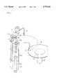
- the disclosed spin coating apparatusincludes a chuck 10 which by application of a suction force horizontally holds a substrate W.
- the substrateis rotated by a motor (not shown) around a vertical axis with a rotation shaft 12 vertically and integrally disposed.
- the disclosed spin coating apparatusalso includes a nozzle which supplies an SOG material onto the substrate W which is held by the chuck 10.
- a cup which is disposed to surround the substrate Wis held by the chuck 10 so as to collect excessive amounts of the SOG material spatters from the peripheral edge of the substrate W, etc.
- the SOG materialis dropped down from the nozzle onto a central portion of the substrate W and is spread all over the substrate W as a thin film, so that an SOG film is formed on the surface of the substrate W.
- a film removal mechanism 14which dissolves and removes the SOG film from a peripheral edge portion of the substrate W.
- a needle-shaped nozzle 16despenses and supplies a film dissolving liquid to the substrate W.
- a nozzle supporting arm 18seats the needle-shaped nozzle 16 at the tip thereof.
- a rotation shaft 20is held upright with a top end portion fixed to an edge portion of the arm 18.
- a movable frame 22supports the rotation shaft 20 rotatably around a vertical axis.
- An air cylinder 24is fixed to an apparatus frame not shown and has a piston rod with a tip portion thereof fixed to the movable frame 22 so as to move the movable frame 22 in a vertical direction.
- a pair of guide rollers 26, 26are attached to the nozzle supporting arm 18.
- a guide rail 28is fixed upright to the apparatus frame not shown with an upper portion bent in a direction away from the substrate W which is held by the chuck 10, and is fitted with the guide rollers 26, 26 which hold the guide rail 28 from both sides.
- the film removal mechanism 14having such a structure as described above operates as follows.
- the nozzle supporting arm 18turns away at a large distance from the substrate W as shown by the solid line, whereby the needle-shaped nozzle 16 is held at an upper stand-by position.
- movable frame 22moves downward as the air cylinder 24 is driven to shrink, in accordance with that the arm 18, guided by the guide rail 28, turns to come close to the substrate W.
- the needle-shaped nozzle 16is consequently located at the lowest position so that the tip portion of the needle-shaped nozzle 16 faces the peripheral edge portion of the substrate W with a predetermined gap, e.g., 1 mm.
- the film dissolving liquidis ejected from the needle-shaped nozzle 16 onto the peripheral edge portion of the substrate W, which is rotating, so that the unwanted SOG film is dissolved at and removed from the entire peripheral edge portion of the substrate W.
- IPAisopropyl alcohol
- butyl acetateisopropyl alcohol
- FIG. 3shows a change in film thickness at a boundary portion between a covered portion A covered with the SOG film and a removed portion B where the SOG film is dissolved and removed from the peripheral edge portion of the substrate W.
- the symbol Sdenotes the position of the surface of the substrate.
- IPAwas used as the film dissolving liquid
- the processing timewas 0.5 seconds
- the rotation speed of the substratewas 1,700 rpm
- the diameter of the needle-shaped nozzlewas 0.49 mm
- the flow rate of IPA injected from the needle-shaped nozzlewas 25 cc/min.
- HSG-2209which is available from Hitachi Chemical Co., Ltd. was used.
- the present inventionis directed to a film dissolution method of dissolving a silica-based coating film formed on a surface of a substrate, comprising steps of (a) preparing a needle-shaped nozzole, (b) preparing a substrate on a surface of which a silica-based coating film is formed, (c) obtaining, as film dissolving liquid, a solvent or a mixture of two or more solvents selected from a group which consists of, ⁇ -butyrolactone, ethyl lactate and ethyl pyruvate, (d) holding the substrate horizontally, (e) rotating the substrate around a vertical axis, and (f) injecting the film dissolving liquid from the needle-shaped nozzle onto a peripheral edge portion of the substrate so that an unwanted coating film is dissolved at and removed from the peripheral edge portion of the substrate.
- the film dissolution methodsince cyclohexanone, ⁇ -butyl lactone, ethyl lactate, ethyl pyruvate, or a mixture of two or more thereof is used as the film dissolving liquid in order to dissolve and remove an unwanted portion of the SOG film, which is formed on a surface of the substrate, from the peripheral edge portion of the substrate, a swelling at an end portion of the SOG film is not created or is suppressed small. This prevents a crack at the end portion of the SOG film, and hence, generation of particles due to a damage at the swelling portion of the SOG film.
- an object of the present inventionis to provide a film dissolution method, whereby during dissolution and removal of an unwanted portion of an SOG film, which is created on a surface of a substrate, from a peripheral edge portion of the substrate, a swelling is not created or is suppressed at an end portion of the SOG film so that a crack is not created at the end portion of the SOG film and generation of particles due to a damage at a swelling portion of the SOG film is prevented.
- FIG. 1is a perspective view showing an example of a structure of a spin coating apparatus which includes a film removal mechanism
- FIG. 2is a graph showing a change in film thickness at a boundary portion between a covered portion A covered with an SOG film and a removed portion B where the SOG film is dissolved at and removed from a peripheral edge portion of a substrate using cyclohexanone, i.e., one of the film dissolving liquids which are used in a method according to the present invention.
- FIG. 3is a graph showing a change in film thickness at a boundary portion between the covered portion A covered with the SOG film and the removed portion B where the SOG film is dissolved at and removed from a peripheral edge portion of a substrate using IPA, i.e., the film dissolving liquids which are conventionally used.
- either one of cyclohexanone, ⁇ -butyrolactone, ethyl lactate and ethyl pyruvateis used as a film dissolving liquid to dissolve an SOG film.
- a film dissolving liquidsuch as cyclohexane
- the film dissolving liquidis ejected from a needle-shaped nozzle 16 onto a peripheral edge portion of a substrate W which, with a SOG film formed on a surface thereof, is held and rotated by a chuck 10. Accordingly, an unwanted portion of the SOG film is dissolved at and removed from the entire peripheral edge portion of the substrate W by the film dissolving liquid.
- FIG. 2shows a change in film thickness at a boundary portion between a covered portion A that is covered with an SOG film and a removed portion B where the SOG film is dissolved at and removed from the peripheral edge portion of the substrate using cyclohexanone as the film dissolving liquid.
- the processing timewas 0.5 seconds
- the rotation speed of the substratewas 1,700 rpm
- the diameter of the needle-shaped nozzlewas 0.49 mm
- the flow rate of cyclohexanone ejected from the needle-like nozzlewas 15 cc/min.
- the SOG film on the surface of the substratewas formed using HSG-2209 (brand name) which is available from Hitachi Chemical Co., Ltd.
- a film swelling portion C as that shown in FIG. 3is not created at an end portion of the SOG film.
- the SOG materialwas changed among various types to form an SOG film on a surface of each substrate.
- cyclohexanone, ⁇ -butyrolactone, ethyl lactate and ethyl pyruvatewere use as the film dissolving liquid so that the SOG films were dissolved at and removed from a peripheral edge portion of each substrate.
- Table 1shows the results.
- the conditions for processingwere the same as described above.
- chemicals A to Gwhich were used as the SOG material are as follows: chemical A was TYPE7 (brand name) available from Tokyo Ohka Kogyo Co., Ltd.; chemical B was SF-1014 (brand name) available from Sumitomo Chemical Co., Ltd.; chemical C was to HSG-2209 (brand name) available from Hitachi Chemical Co., Ltd.; chemical D was Accuglass (brand name) available from Allied Signal Inc.; chemical E was TYPE2 (brand name) available from Tokyo Ohka Kogyo Co., Ltd.; chemical F was FOX-15 (brand name) available from Dow Corning Toray Silicone Co., Ltd.; and chemical G was Ceramate CIP (brand name) available from Catalysts & Chemicals Industries Co., Ltd. Of these chemicals, chemicals A to D are organic SOG materials while chemicals E to G are inorganic SOG materials.
Landscapes
- Engineering & Computer Science (AREA)
- Chemical & Material Sciences (AREA)
- Chemical Kinetics & Catalysis (AREA)
- Physics & Mathematics (AREA)
- Power Engineering (AREA)
- Microelectronics & Electronic Packaging (AREA)
- Computer Hardware Design (AREA)
- Manufacturing & Machinery (AREA)
- General Physics & Mathematics (AREA)
- Condensed Matter Physics & Semiconductors (AREA)
- General Chemical & Material Sciences (AREA)
- Health & Medical Sciences (AREA)
- Organic Chemistry (AREA)
- Wood Science & Technology (AREA)
- Oil, Petroleum & Natural Gas (AREA)
- Emergency Medicine (AREA)
- Life Sciences & Earth Sciences (AREA)
- Application Of Or Painting With Fluid Materials (AREA)
- Coating Apparatus (AREA)
- Formation Of Insulating Films (AREA)
- Cleaning Or Drying Semiconductors (AREA)
- Exposure Of Semiconductors, Excluding Electron Or Ion Beam Exposure (AREA)
Abstract
Description
TABLE 1 __________________________________________________________________________ IPA Cyclohexanone γ-Butyrolactone Ethyl lactate Ethyl pyruvate Appear- Appear- Appear- Appear- Appear- Chemicals ance Swelling ance Swelling ance Swelling ance Swelling ance Swelling __________________________________________________________________________Chemical A excellent ≧10,000 excellent none excellent none excellent ≧1,500 excellent none (Å) (Å) Chemical B excellent ≧10,000 excellent none excellent none excellent none excellent none (Å) Chemical C some none excellent none excellent none excellent none excellent none remained Chemical D excellent ≧2,500 excellent ≧1,000 excellent none excellent ≧2,500 excellent ≧500 (Å) (Å) (Å) (Å) Chemical E excellent ≧10,000 excellent ≧3,000 excellent none excellent ≧2,500 excellent ≧3,000 (Å) (Å) (Å) (Å) Chemical F unusable excellent none unusable unusable unusable Chemical G unusable excellent none -- -- -- __________________________________________________________________________
Claims (4)
Applications Claiming Priority (2)
| Application Number | Priority Date | Filing Date | Title |
|---|---|---|---|
| JP05247596AJP3740207B2 (en) | 1996-02-13 | 1996-02-13 | Method for dissolving silica-based coating film formed on substrate surface |
| JP8-052475 | 1996-02-13 |
Publications (1)
| Publication Number | Publication Date |
|---|---|
| US5779928Atrue US5779928A (en) | 1998-07-14 |
Family
ID=12915756
Family Applications (1)
| Application Number | Title | Priority Date | Filing Date |
|---|---|---|---|
| US08/799,478Expired - LifetimeUS5779928A (en) | 1996-02-13 | 1997-02-12 | Film dissolution method of dissolving silica-based coating film formed on surface of a substrate |
Country Status (3)
| Country | Link |
|---|---|
| US (1) | US5779928A (en) |
| JP (1) | JP3740207B2 (en) |
| KR (1) | KR100230090B1 (en) |
Cited By (11)
| Publication number | Priority date | Publication date | Assignee | Title |
|---|---|---|---|---|
| US5879577A (en)* | 1996-12-13 | 1999-03-09 | Taiwan Semiconductor Manufacturing Company Ltd. | Process for wafer peripheral edge defect reduction |
| EP0924754A3 (en)* | 1997-12-19 | 1999-09-08 | Sharp Kabushiki Kaisha | Low temperature system and method for CVD copper removal |
| US6033988A (en)* | 1997-01-31 | 2000-03-07 | Kawasaki Steel Corporation | Film forming methods |
| US20030054616A1 (en)* | 2001-08-29 | 2003-03-20 | Honeywell International Inc. | Electronic devices and methods of manufacture |
| US6565928B2 (en)* | 1999-03-08 | 2003-05-20 | Tokyo Electron Limited | Film forming method and film forming apparatus |
| US20030227005A1 (en)* | 2002-02-06 | 2003-12-11 | Arch Specialty Chemicals, Inc. | Semiconductor stress buffer coating edge bead removal compositions and method for their use |
| US20050027089A1 (en)* | 2001-12-27 | 2005-02-03 | Yasuo Shimizu | Solvent for treating polysilazane and method of treating polysilazane with the solvent |
| US20080090341A1 (en)* | 2006-10-12 | 2008-04-17 | Semiconductor Energy Laboratory Co., Ltd. | Method for manufacturing display device, and etching apparatus |
| US20080102211A1 (en)* | 2005-02-02 | 2008-05-01 | Hideki Matsuo | Polysilazane-Treating Solvent and Method for Treating Polysilazane by Using Such Solvent |
| EP1158573A4 (en)* | 1999-10-15 | 2008-09-24 | Ebara Corp | Method and apparatus for forming interconnection |
| RU2630520C2 (en)* | 2012-03-29 | 2017-09-11 | золар-земи ГмбХ | Method and device for removing coatings from substrates |
Families Citing this family (2)
| Publication number | Priority date | Publication date | Assignee | Title |
|---|---|---|---|---|
| US6005586A (en)* | 1996-02-17 | 1999-12-21 | Fuji Xerox Co., Ltd. | Drawing processing apparatus |
| JP4745365B2 (en)* | 2008-04-10 | 2011-08-10 | 東京エレクトロン株式会社 | Substrate processing method and substrate processing apparatus |
Citations (6)
| Publication number | Priority date | Publication date | Assignee | Title |
|---|---|---|---|---|
| US4011351A (en)* | 1975-01-29 | 1977-03-08 | International Business Machines Corporation | Preparation of resist image with methacrylate polymers |
| JPH0230132A (en)* | 1988-07-19 | 1990-01-31 | Nec Corp | Manufacture of semiconductor device |
| JPH04171820A (en)* | 1990-11-05 | 1992-06-19 | Nec Kyushu Ltd | Method of forming coating |
| US5328871A (en)* | 1991-02-18 | 1994-07-12 | Sharp Kabushiki Kaisha | Manufacturing process for semiconductor device |
| JPH0897205A (en)* | 1994-09-21 | 1996-04-12 | Mitsubishi Electric Corp | SOG film coating method |
| JPH08264412A (en)* | 1995-03-20 | 1996-10-11 | Nittetsu Semiconductor Kk | Application of application liquid in semiconductor device manufacture process |
- 1996
- 1996-02-13JPJP05247596Apatent/JP3740207B2/ennot_activeExpired - Fee Related
- 1997
- 1997-01-07KRKR1019970000191Apatent/KR100230090B1/ennot_activeExpired - Fee Related
- 1997-02-12USUS08/799,478patent/US5779928A/ennot_activeExpired - Lifetime
Patent Citations (6)
| Publication number | Priority date | Publication date | Assignee | Title |
|---|---|---|---|---|
| US4011351A (en)* | 1975-01-29 | 1977-03-08 | International Business Machines Corporation | Preparation of resist image with methacrylate polymers |
| JPH0230132A (en)* | 1988-07-19 | 1990-01-31 | Nec Corp | Manufacture of semiconductor device |
| JPH04171820A (en)* | 1990-11-05 | 1992-06-19 | Nec Kyushu Ltd | Method of forming coating |
| US5328871A (en)* | 1991-02-18 | 1994-07-12 | Sharp Kabushiki Kaisha | Manufacturing process for semiconductor device |
| JPH0897205A (en)* | 1994-09-21 | 1996-04-12 | Mitsubishi Electric Corp | SOG film coating method |
| JPH08264412A (en)* | 1995-03-20 | 1996-10-11 | Nittetsu Semiconductor Kk | Application of application liquid in semiconductor device manufacture process |
Non-Patent Citations (2)
| Title |
|---|
| "Corrosion of Silica Glass by Aqueous Solutions of Organic Compounds"; Rybarikova et al.; abstract only; Ceram.-Silik (1996), 40(3). |
| Corrosion of Silica Glass by Aqueous Solutions of Organic Compounds ; Rybarikova et al.; abstract only; Ceram. Silik (1996), 40(3).* |
Cited By (16)
| Publication number | Priority date | Publication date | Assignee | Title |
|---|---|---|---|---|
| US5879577A (en)* | 1996-12-13 | 1999-03-09 | Taiwan Semiconductor Manufacturing Company Ltd. | Process for wafer peripheral edge defect reduction |
| US6033988A (en)* | 1997-01-31 | 2000-03-07 | Kawasaki Steel Corporation | Film forming methods |
| EP0924754A3 (en)* | 1997-12-19 | 1999-09-08 | Sharp Kabushiki Kaisha | Low temperature system and method for CVD copper removal |
| US6565928B2 (en)* | 1999-03-08 | 2003-05-20 | Tokyo Electron Limited | Film forming method and film forming apparatus |
| EP1158573A4 (en)* | 1999-10-15 | 2008-09-24 | Ebara Corp | Method and apparatus for forming interconnection |
| US20030054616A1 (en)* | 2001-08-29 | 2003-03-20 | Honeywell International Inc. | Electronic devices and methods of manufacture |
| US7344603B2 (en)* | 2001-12-27 | 2008-03-18 | Az Electronic Materials Usa Corp. | Solvent for treating polysilazane and method of treating polysilazane with the solvent |
| US20050027089A1 (en)* | 2001-12-27 | 2005-02-03 | Yasuo Shimizu | Solvent for treating polysilazane and method of treating polysilazane with the solvent |
| EP1554033A4 (en)* | 2002-02-06 | 2007-12-05 | Fujifilm Electronic Materials | Improved semiconductor stress buffer coating edge bead removal compositions and method for their use |
| US7335319B2 (en) | 2002-02-06 | 2008-02-26 | Arch Specialty Chemicals, Inc. | Semiconductor stress buffer coating edge bead removal compositions and method for their use |
| US20040224516A1 (en)* | 2002-02-06 | 2004-11-11 | Arch Specialty Chemicals, Inc. | Semiconductor stress buffer coating edge bead removal compositions and method for their use |
| US20030227005A1 (en)* | 2002-02-06 | 2003-12-11 | Arch Specialty Chemicals, Inc. | Semiconductor stress buffer coating edge bead removal compositions and method for their use |
| US20080102211A1 (en)* | 2005-02-02 | 2008-05-01 | Hideki Matsuo | Polysilazane-Treating Solvent and Method for Treating Polysilazane by Using Such Solvent |
| US20080090341A1 (en)* | 2006-10-12 | 2008-04-17 | Semiconductor Energy Laboratory Co., Ltd. | Method for manufacturing display device, and etching apparatus |
| US7968453B2 (en)* | 2006-10-12 | 2011-06-28 | Semiconductor Energy Laboratory Co., Ltd. | Method for manufacturing display device, and etching apparatus |
| RU2630520C2 (en)* | 2012-03-29 | 2017-09-11 | золар-земи ГмбХ | Method and device for removing coatings from substrates |
Also Published As
| Publication number | Publication date |
|---|---|
| KR970063422A (en) | 1997-09-12 |
| JPH09220505A (en) | 1997-08-26 |
| KR100230090B1 (en) | 1999-11-15 |
| JP3740207B2 (en) | 2006-02-01 |
Similar Documents
| Publication | Publication Date | Title |
|---|---|---|
| US5779928A (en) | Film dissolution method of dissolving silica-based coating film formed on surface of a substrate | |
| US10811283B2 (en) | Substrate cleaning method, substrate cleaning system, and memory medium | |
| US4113492A (en) | Spin coating process | |
| KR102292896B1 (en) | Substrate processing method and substrate processing apparatus | |
| US6255228B1 (en) | Method for removing contaminants from a semiconductor wafer | |
| US6770151B1 (en) | Drying a substrate using a combination of substrate processing technologies | |
| KR20210103516A (en) | Substrate cleaning solution and method of manufacturing a cleaned substrate and device using the same | |
| US5392989A (en) | Nozzle assembly for dispensing liquid | |
| US20040221954A1 (en) | Coating apparatus and coating method | |
| CN101371350A (en) | Integrated circuit with anti-reflection coating | |
| JP3168642B2 (en) | Coating removal method and apparatus | |
| EP3576134A1 (en) | Substrate processing method and substrate processing apparatus | |
| JP4105269B2 (en) | Film formation method | |
| JP2793554B2 (en) | Method for manufacturing semiconductor device | |
| JP2004319720A (en) | Apparatus and method for substrate washing | |
| JP2659306B2 (en) | Substrate edge cleaning device | |
| JPH05259050A (en) | Spin coating on semiconductor substrate and device | |
| JP2840182B2 (en) | Rotary coating method for substrate and rotary coating apparatus for substrate | |
| JP2909362B2 (en) | Substrate holding device | |
| TWI813405B (en) | Substrate processing method and substrate processing apparatus | |
| KR100513436B1 (en) | Thin film removing apparatus | |
| JPH05259063A (en) | Semiconductor substrate spin coating method | |
| JPH06283417A (en) | Film-coating device | |
| JPH0628224Y2 (en) | Substrate rotation processing device | |
| JP2000100682A (en) | Edge part removing method for substrate coat |
Legal Events
| Date | Code | Title | Description |
|---|---|---|---|
| AS | Assignment | Owner name:DAINIPPON SCREEN MFG. CO., LTD. (CORPORATION-JAPAN Free format text:ASSIGNMENT OF ASSIGNORS INTEREST;ASSIGNORS:YAMASHITA, TETSURO;MITSUHASHI, TSUYOSHI;YABE, MANABU;REEL/FRAME:008466/0269;SIGNING DATES FROM 19961219 TO 19961225 | |
| FEPP | Fee payment procedure | Free format text:PAYOR NUMBER ASSIGNED (ORIGINAL EVENT CODE: ASPN); ENTITY STATUS OF PATENT OWNER: LARGE ENTITY | |
| STCF | Information on status: patent grant | Free format text:PATENTED CASE | |
| FPAY | Fee payment | Year of fee payment:4 | |
| FPAY | Fee payment | Year of fee payment:8 | |
| AS | Assignment | Owner name:SOKUDO CO., LTD., JAPAN Free format text:ASSIGNMENT OF ASSIGNORS INTEREST;ASSIGNOR:DAINIPPON SCREEN MFG. CO., LTD.;REEL/FRAME:019365/0268 Effective date:20070409 | |
| FPAY | Fee payment | Year of fee payment:12 | |
| AS | Assignment | Owner name:SCREEN SEMICONDUCTOR SOLUTIONS CO., LTD., JAPAN Free format text:CHANGE OF NAME;ASSIGNOR:SOKUDO CO., LTD.;REEL/FRAME:034150/0849 Effective date:20140807 |