US5779839A - Method of manufacturing an enclosed transceiver - Google Patents
Method of manufacturing an enclosed transceiverDownload PDFInfo
- Publication number
- US5779839A US5779839AUS08/947,681US94768197AUS5779839AUS 5779839 AUS5779839 AUS 5779839AUS 94768197 AUS94768197 AUS 94768197AUS 5779839 AUS5779839 AUS 5779839A
- Authority
- US
- United States
- Prior art keywords
- battery
- transceiver
- enclosed
- antenna
- depositing
- Prior art date
- Legal status (The legal status is an assumption and is not a legal conclusion. Google has not performed a legal analysis and makes no representation as to the accuracy of the status listed.)
- Expired - Lifetime
Links
Images


Classifications
- H—ELECTRICITY
- H01—ELECTRIC ELEMENTS
- H01Q—ANTENNAS, i.e. RADIO AERIALS
- H01Q1/00—Details of, or arrangements associated with, antennas
- H01Q1/12—Supports; Mounting means
- H01Q1/22—Supports; Mounting means by structural association with other equipment or articles
- H01Q1/2208—Supports; Mounting means by structural association with other equipment or articles associated with components used in interrogation type services, i.e. in systems for information exchange between an interrogator/reader and a tag/transponder, e.g. in Radio Frequency Identification [RFID] systems
- H01Q1/2225—Supports; Mounting means by structural association with other equipment or articles associated with components used in interrogation type services, i.e. in systems for information exchange between an interrogator/reader and a tag/transponder, e.g. in Radio Frequency Identification [RFID] systems used in active tags, i.e. provided with its own power source or in passive tags, i.e. deriving power from RF signal
- G—PHYSICS
- G01—MEASURING; TESTING
- G01S—RADIO DIRECTION-FINDING; RADIO NAVIGATION; DETERMINING DISTANCE OR VELOCITY BY USE OF RADIO WAVES; LOCATING OR PRESENCE-DETECTING BY USE OF THE REFLECTION OR RERADIATION OF RADIO WAVES; ANALOGOUS ARRANGEMENTS USING OTHER WAVES
- G01S13/00—Systems using the reflection or reradiation of radio waves, e.g. radar systems; Analogous systems using reflection or reradiation of waves whose nature or wavelength is irrelevant or unspecified
- G01S13/74—Systems using reradiation of radio waves, e.g. secondary radar systems; Analogous systems
- G01S13/75—Systems using reradiation of radio waves, e.g. secondary radar systems; Analogous systems using transponders powered from received waves, e.g. using passive transponders, or using passive reflectors
- G01S13/751—Systems using reradiation of radio waves, e.g. secondary radar systems; Analogous systems using transponders powered from received waves, e.g. using passive transponders, or using passive reflectors wherein the responder or reflector radiates a coded signal
- G01S13/758—Systems using reradiation of radio waves, e.g. secondary radar systems; Analogous systems using transponders powered from received waves, e.g. using passive transponders, or using passive reflectors wherein the responder or reflector radiates a coded signal using a signal generator powered by the interrogation signal
- G—PHYSICS
- G01—MEASURING; TESTING
- G01S—RADIO DIRECTION-FINDING; RADIO NAVIGATION; DETERMINING DISTANCE OR VELOCITY BY USE OF RADIO WAVES; LOCATING OR PRESENCE-DETECTING BY USE OF THE REFLECTION OR RERADIATION OF RADIO WAVES; ANALOGOUS ARRANGEMENTS USING OTHER WAVES
- G01S13/00—Systems using the reflection or reradiation of radio waves, e.g. radar systems; Analogous systems using reflection or reradiation of waves whose nature or wavelength is irrelevant or unspecified
- G01S13/74—Systems using reradiation of radio waves, e.g. secondary radar systems; Analogous systems
- G01S13/76—Systems using reradiation of radio waves, e.g. secondary radar systems; Analogous systems wherein pulse-type signals are transmitted
- G01S13/767—Responders; Transponders
- G—PHYSICS
- G06—COMPUTING OR CALCULATING; COUNTING
- G06K—GRAPHICAL DATA READING; PRESENTATION OF DATA; RECORD CARRIERS; HANDLING RECORD CARRIERS
- G06K19/00—Record carriers for use with machines and with at least a part designed to carry digital markings
- G06K19/06—Record carriers for use with machines and with at least a part designed to carry digital markings characterised by the kind of the digital marking, e.g. shape, nature, code
- G06K19/067—Record carriers with conductive marks, printed circuits or semiconductor circuit elements, e.g. credit or identity cards also with resonating or responding marks without active components
- G06K19/07—Record carriers with conductive marks, printed circuits or semiconductor circuit elements, e.g. credit or identity cards also with resonating or responding marks without active components with integrated circuit chips
- G06K19/0723—Record carriers with conductive marks, printed circuits or semiconductor circuit elements, e.g. credit or identity cards also with resonating or responding marks without active components with integrated circuit chips the record carrier comprising an arrangement for non-contact communication, e.g. wireless communication circuits on transponder cards, non-contact smart cards or RFIDs
- G—PHYSICS
- G06—COMPUTING OR CALCULATING; COUNTING
- G06K—GRAPHICAL DATA READING; PRESENTATION OF DATA; RECORD CARRIERS; HANDLING RECORD CARRIERS
- G06K19/00—Record carriers for use with machines and with at least a part designed to carry digital markings
- G06K19/06—Record carriers for use with machines and with at least a part designed to carry digital markings characterised by the kind of the digital marking, e.g. shape, nature, code
- G06K19/067—Record carriers with conductive marks, printed circuits or semiconductor circuit elements, e.g. credit or identity cards also with resonating or responding marks without active components
- G06K19/07—Record carriers with conductive marks, printed circuits or semiconductor circuit elements, e.g. credit or identity cards also with resonating or responding marks without active components with integrated circuit chips
- G06K19/073—Special arrangements for circuits, e.g. for protecting identification code in memory
- G—PHYSICS
- G06—COMPUTING OR CALCULATING; COUNTING
- G06K—GRAPHICAL DATA READING; PRESENTATION OF DATA; RECORD CARRIERS; HANDLING RECORD CARRIERS
- G06K19/00—Record carriers for use with machines and with at least a part designed to carry digital markings
- G06K19/06—Record carriers for use with machines and with at least a part designed to carry digital markings characterised by the kind of the digital marking, e.g. shape, nature, code
- G06K19/067—Record carriers with conductive marks, printed circuits or semiconductor circuit elements, e.g. credit or identity cards also with resonating or responding marks without active components
- G06K19/07—Record carriers with conductive marks, printed circuits or semiconductor circuit elements, e.g. credit or identity cards also with resonating or responding marks without active components with integrated circuit chips
- G06K19/077—Constructional details, e.g. mounting of circuits in the carrier
- G06K19/07749—Constructional details, e.g. mounting of circuits in the carrier the record carrier being capable of non-contact communication, e.g. constructional details of the antenna of a non-contact smart card
- G06K19/07773—Antenna details
- G06K19/07786—Antenna details the antenna being of the HF type, such as a dipole
- H—ELECTRICITY
- H01—ELECTRIC ELEMENTS
- H01L—SEMICONDUCTOR DEVICES NOT COVERED BY CLASS H10
- H01L24/00—Arrangements for connecting or disconnecting semiconductor or solid-state bodies; Methods or apparatus related thereto
- H01L24/01—Means for bonding being attached to, or being formed on, the surface to be connected, e.g. chip-to-package, die-attach, "first-level" interconnects; Manufacturing methods related thereto
- H01L24/18—High density interconnect [HDI] connectors; Manufacturing methods related thereto
- H01L24/23—Structure, shape, material or disposition of the high density interconnect connectors after the connecting process
- H01L24/24—Structure, shape, material or disposition of the high density interconnect connectors after the connecting process of an individual high density interconnect connector
- H—ELECTRICITY
- H01—ELECTRIC ELEMENTS
- H01L—SEMICONDUCTOR DEVICES NOT COVERED BY CLASS H10
- H01L24/00—Arrangements for connecting or disconnecting semiconductor or solid-state bodies; Methods or apparatus related thereto
- H01L24/80—Methods for connecting semiconductor or other solid state bodies using means for bonding being attached to, or being formed on, the surface to be connected
- H01L24/82—Methods for connecting semiconductor or other solid state bodies using means for bonding being attached to, or being formed on, the surface to be connected by forming build-up interconnects at chip-level, e.g. for high density interconnects [HDI]
- H—ELECTRICITY
- H01—ELECTRIC ELEMENTS
- H01Q—ANTENNAS, i.e. RADIO AERIALS
- H01Q1/00—Details of, or arrangements associated with, antennas
- H01Q1/12—Supports; Mounting means
- H01Q1/22—Supports; Mounting means by structural association with other equipment or articles
- H—ELECTRICITY
- H01—ELECTRIC ELEMENTS
- H01Q—ANTENNAS, i.e. RADIO AERIALS
- H01Q1/00—Details of, or arrangements associated with, antennas
- H01Q1/36—Structural form of radiating elements, e.g. cone, spiral, umbrella; Particular materials used therewith
- H01Q1/38—Structural form of radiating elements, e.g. cone, spiral, umbrella; Particular materials used therewith formed by a conductive layer on an insulating support
- H—ELECTRICITY
- H01—ELECTRIC ELEMENTS
- H01Q—ANTENNAS, i.e. RADIO AERIALS
- H01Q1/00—Details of, or arrangements associated with, antennas
- H01Q1/44—Details of, or arrangements associated with, antennas using equipment having another main function to serve additionally as an antenna, e.g. means for giving an antenna an aesthetic aspect
- H—ELECTRICITY
- H01—ELECTRIC ELEMENTS
- H01Q—ANTENNAS, i.e. RADIO AERIALS
- H01Q9/00—Electrically-short antennas having dimensions not more than twice the operating wavelength and consisting of conductive active radiating elements
- H01Q9/04—Resonant antennas
- H01Q9/16—Resonant antennas with feed intermediate between the extremities of the antenna, e.g. centre-fed dipole
- H01Q9/28—Conical, cylindrical, cage, strip, gauze, or like elements having an extended radiating surface; Elements comprising two conical surfaces having collinear axes and adjacent apices and fed by two-conductor transmission lines
- H01Q9/285—Planar dipole
- H—ELECTRICITY
- H04—ELECTRIC COMMUNICATION TECHNIQUE
- H04L—TRANSMISSION OF DIGITAL INFORMATION, e.g. TELEGRAPHIC COMMUNICATION
- H04L61/00—Network arrangements, protocols or services for addressing or naming
- H04L61/35—Network arrangements, protocols or services for addressing or naming involving non-standard use of addresses for implementing network functionalities, e.g. coding subscription information within the address or functional addressing, i.e. assigning an address to a function
- H—ELECTRICITY
- H04—ELECTRIC COMMUNICATION TECHNIQUE
- H04L—TRANSMISSION OF DIGITAL INFORMATION, e.g. TELEGRAPHIC COMMUNICATION
- H04L61/00—Network arrangements, protocols or services for addressing or naming
- H04L61/50—Address allocation
- H04L61/5038—Address allocation for local use, e.g. in LAN or USB networks, or in a controller area network [CAN]
- H—ELECTRICITY
- H04—ELECTRIC COMMUNICATION TECHNIQUE
- H04L—TRANSMISSION OF DIGITAL INFORMATION, e.g. TELEGRAPHIC COMMUNICATION
- H04L61/00—Network arrangements, protocols or services for addressing or naming
- H04L61/50—Address allocation
- H04L61/5046—Resolving address allocation conflicts; Testing of addresses
- H—ELECTRICITY
- H04—ELECTRIC COMMUNICATION TECHNIQUE
- H04L—TRANSMISSION OF DIGITAL INFORMATION, e.g. TELEGRAPHIC COMMUNICATION
- H04L61/00—Network arrangements, protocols or services for addressing or naming
- H04L61/50—Address allocation
- H04L61/5084—Providing for device mobility
- H—ELECTRICITY
- H04—ELECTRIC COMMUNICATION TECHNIQUE
- H04L—TRANSMISSION OF DIGITAL INFORMATION, e.g. TELEGRAPHIC COMMUNICATION
- H04L61/00—Network arrangements, protocols or services for addressing or naming
- H04L61/50—Address allocation
- H04L61/5092—Address allocation by self-assignment, e.g. picking addresses at random and testing if they are already in use
- G—PHYSICS
- G07—CHECKING-DEVICES
- G07B—TICKET-ISSUING APPARATUS; FARE-REGISTERING APPARATUS; FRANKING APPARATUS
- G07B17/00—Franking apparatus
- G07B17/00459—Details relating to mailpieces in a franking system
- G07B17/00508—Printing or attaching on mailpieces
- G07B2017/00612—Attaching item on mailpiece
- G07B2017/00629—Circuit, e.g. transponder
- H—ELECTRICITY
- H01—ELECTRIC ELEMENTS
- H01L—SEMICONDUCTOR DEVICES NOT COVERED BY CLASS H10
- H01L2224/00—Indexing scheme for arrangements for connecting or disconnecting semiconductor or solid-state bodies and methods related thereto as covered by H01L24/00
- H01L2224/01—Means for bonding being attached to, or being formed on, the surface to be connected, e.g. chip-to-package, die-attach, "first-level" interconnects; Manufacturing methods related thereto
- H01L2224/10—Bump connectors; Manufacturing methods related thereto
- H01L2224/15—Structure, shape, material or disposition of the bump connectors after the connecting process
- H01L2224/16—Structure, shape, material or disposition of the bump connectors after the connecting process of an individual bump connector
- H—ELECTRICITY
- H01—ELECTRIC ELEMENTS
- H01L—SEMICONDUCTOR DEVICES NOT COVERED BY CLASS H10
- H01L2224/00—Indexing scheme for arrangements for connecting or disconnecting semiconductor or solid-state bodies and methods related thereto as covered by H01L24/00
- H01L2224/01—Means for bonding being attached to, or being formed on, the surface to be connected, e.g. chip-to-package, die-attach, "first-level" interconnects; Manufacturing methods related thereto
- H01L2224/18—High density interconnect [HDI] connectors; Manufacturing methods related thereto
- H01L2224/23—Structure, shape, material or disposition of the high density interconnect connectors after the connecting process
- H01L2224/24—Structure, shape, material or disposition of the high density interconnect connectors after the connecting process of an individual high density interconnect connector
- H01L2224/2405—Shape
- H01L2224/24051—Conformal with the semiconductor or solid-state device
- H—ELECTRICITY
- H01—ELECTRIC ELEMENTS
- H01L—SEMICONDUCTOR DEVICES NOT COVERED BY CLASS H10
- H01L2224/00—Indexing scheme for arrangements for connecting or disconnecting semiconductor or solid-state bodies and methods related thereto as covered by H01L24/00
- H01L2224/01—Means for bonding being attached to, or being formed on, the surface to be connected, e.g. chip-to-package, die-attach, "first-level" interconnects; Manufacturing methods related thereto
- H01L2224/18—High density interconnect [HDI] connectors; Manufacturing methods related thereto
- H01L2224/23—Structure, shape, material or disposition of the high density interconnect connectors after the connecting process
- H01L2224/24—Structure, shape, material or disposition of the high density interconnect connectors after the connecting process of an individual high density interconnect connector
- H01L2224/241—Disposition
- H01L2224/24151—Connecting between a semiconductor or solid-state body and an item not being a semiconductor or solid-state body, e.g. chip-to-substrate, chip-to-passive
- H01L2224/24221—Connecting between a semiconductor or solid-state body and an item not being a semiconductor or solid-state body, e.g. chip-to-substrate, chip-to-passive the body and the item being stacked
- H01L2224/24225—Connecting between a semiconductor or solid-state body and an item not being a semiconductor or solid-state body, e.g. chip-to-substrate, chip-to-passive the body and the item being stacked the item being non-metallic, e.g. insulating substrate with or without metallisation
- H01L2224/24226—Connecting between a semiconductor or solid-state body and an item not being a semiconductor or solid-state body, e.g. chip-to-substrate, chip-to-passive the body and the item being stacked the item being non-metallic, e.g. insulating substrate with or without metallisation the HDI interconnect connecting to the same level of the item at which the semiconductor or solid-state body is mounted, e.g. the item being planar
- H—ELECTRICITY
- H01—ELECTRIC ELEMENTS
- H01L—SEMICONDUCTOR DEVICES NOT COVERED BY CLASS H10
- H01L2224/00—Indexing scheme for arrangements for connecting or disconnecting semiconductor or solid-state bodies and methods related thereto as covered by H01L24/00
- H01L2224/01—Means for bonding being attached to, or being formed on, the surface to be connected, e.g. chip-to-package, die-attach, "first-level" interconnects; Manufacturing methods related thereto
- H01L2224/18—High density interconnect [HDI] connectors; Manufacturing methods related thereto
- H01L2224/23—Structure, shape, material or disposition of the high density interconnect connectors after the connecting process
- H01L2224/24—Structure, shape, material or disposition of the high density interconnect connectors after the connecting process of an individual high density interconnect connector
- H01L2224/2499—Auxiliary members for HDI interconnects, e.g. spacers, alignment aids
- H01L2224/24996—Auxiliary members for HDI interconnects, e.g. spacers, alignment aids being formed on an item to be connected not being a semiconductor or solid-state body
- H01L2224/24998—Reinforcing structures, e.g. ramp-like support
- H—ELECTRICITY
- H01—ELECTRIC ELEMENTS
- H01L—SEMICONDUCTOR DEVICES NOT COVERED BY CLASS H10
- H01L2224/00—Indexing scheme for arrangements for connecting or disconnecting semiconductor or solid-state bodies and methods related thereto as covered by H01L24/00
- H01L2224/01—Means for bonding being attached to, or being formed on, the surface to be connected, e.g. chip-to-package, die-attach, "first-level" interconnects; Manufacturing methods related thereto
- H01L2224/26—Layer connectors, e.g. plate connectors, solder or adhesive layers; Manufacturing methods related thereto
- H01L2224/31—Structure, shape, material or disposition of the layer connectors after the connecting process
- H01L2224/32—Structure, shape, material or disposition of the layer connectors after the connecting process of an individual layer connector
- H01L2224/321—Disposition
- H01L2224/32151—Disposition the layer connector connecting between a semiconductor or solid-state body and an item not being a semiconductor or solid-state body, e.g. chip-to-substrate, chip-to-passive
- H01L2224/32221—Disposition the layer connector connecting between a semiconductor or solid-state body and an item not being a semiconductor or solid-state body, e.g. chip-to-substrate, chip-to-passive the body and the item being stacked
- H01L2224/32225—Disposition the layer connector connecting between a semiconductor or solid-state body and an item not being a semiconductor or solid-state body, e.g. chip-to-substrate, chip-to-passive the body and the item being stacked the item being non-metallic, e.g. insulating substrate with or without metallisation
- H—ELECTRICITY
- H01—ELECTRIC ELEMENTS
- H01L—SEMICONDUCTOR DEVICES NOT COVERED BY CLASS H10
- H01L2224/00—Indexing scheme for arrangements for connecting or disconnecting semiconductor or solid-state bodies and methods related thereto as covered by H01L24/00
- H01L2224/73—Means for bonding being of different types provided for in two or more of groups H01L2224/10, H01L2224/18, H01L2224/26, H01L2224/34, H01L2224/42, H01L2224/50, H01L2224/63, H01L2224/71
- H01L2224/732—Location after the connecting process
- H01L2224/73251—Location after the connecting process on different surfaces
- H01L2224/73267—Layer and HDI connectors
- H—ELECTRICITY
- H01—ELECTRIC ELEMENTS
- H01L—SEMICONDUCTOR DEVICES NOT COVERED BY CLASS H10
- H01L2224/00—Indexing scheme for arrangements for connecting or disconnecting semiconductor or solid-state bodies and methods related thereto as covered by H01L24/00
- H01L2224/80—Methods for connecting semiconductor or other solid state bodies using means for bonding being attached to, or being formed on, the surface to be connected
- H01L2224/82—Methods for connecting semiconductor or other solid state bodies using means for bonding being attached to, or being formed on, the surface to be connected by forming build-up interconnects at chip-level, e.g. for high density interconnects [HDI]
- H01L2224/82007—Methods for connecting semiconductor or other solid state bodies using means for bonding being attached to, or being formed on, the surface to be connected by forming build-up interconnects at chip-level, e.g. for high density interconnects [HDI] involving a permanent auxiliary member being left in the finished device, e.g. aids for holding or protecting a build-up interconnect during or after the bonding process
- H—ELECTRICITY
- H01—ELECTRIC ELEMENTS
- H01L—SEMICONDUCTOR DEVICES NOT COVERED BY CLASS H10
- H01L2924/00—Indexing scheme for arrangements or methods for connecting or disconnecting semiconductor or solid-state bodies as covered by H01L24/00
- H01L2924/01—Chemical elements
- H01L2924/01027—Cobalt [Co]
- H—ELECTRICITY
- H01—ELECTRIC ELEMENTS
- H01L—SEMICONDUCTOR DEVICES NOT COVERED BY CLASS H10
- H01L2924/00—Indexing scheme for arrangements or methods for connecting or disconnecting semiconductor or solid-state bodies as covered by H01L24/00
- H01L2924/01—Chemical elements
- H01L2924/01029—Copper [Cu]
- H—ELECTRICITY
- H01—ELECTRIC ELEMENTS
- H01L—SEMICONDUCTOR DEVICES NOT COVERED BY CLASS H10
- H01L2924/00—Indexing scheme for arrangements or methods for connecting or disconnecting semiconductor or solid-state bodies as covered by H01L24/00
- H01L2924/01—Chemical elements
- H01L2924/01033—Arsenic [As]
- H—ELECTRICITY
- H01—ELECTRIC ELEMENTS
- H01L—SEMICONDUCTOR DEVICES NOT COVERED BY CLASS H10
- H01L2924/00—Indexing scheme for arrangements or methods for connecting or disconnecting semiconductor or solid-state bodies as covered by H01L24/00
- H01L2924/01—Chemical elements
- H01L2924/01047—Silver [Ag]
- H—ELECTRICITY
- H01—ELECTRIC ELEMENTS
- H01L—SEMICONDUCTOR DEVICES NOT COVERED BY CLASS H10
- H01L2924/00—Indexing scheme for arrangements or methods for connecting or disconnecting semiconductor or solid-state bodies as covered by H01L24/00
- H01L2924/01—Chemical elements
- H01L2924/01079—Gold [Au]
- H—ELECTRICITY
- H01—ELECTRIC ELEMENTS
- H01L—SEMICONDUCTOR DEVICES NOT COVERED BY CLASS H10
- H01L2924/00—Indexing scheme for arrangements or methods for connecting or disconnecting semiconductor or solid-state bodies as covered by H01L24/00
- H01L2924/01—Chemical elements
- H01L2924/01082—Lead [Pb]
- H—ELECTRICITY
- H01—ELECTRIC ELEMENTS
- H01L—SEMICONDUCTOR DEVICES NOT COVERED BY CLASS H10
- H01L2924/00—Indexing scheme for arrangements or methods for connecting or disconnecting semiconductor or solid-state bodies as covered by H01L24/00
- H01L2924/013—Alloys
- H01L2924/014—Solder alloys
- H—ELECTRICITY
- H01—ELECTRIC ELEMENTS
- H01L—SEMICONDUCTOR DEVICES NOT COVERED BY CLASS H10
- H01L2924/00—Indexing scheme for arrangements or methods for connecting or disconnecting semiconductor or solid-state bodies as covered by H01L24/00
- H01L2924/10—Details of semiconductor or other solid state devices to be connected
- H01L2924/11—Device type
- H01L2924/14—Integrated circuits
- H—ELECTRICITY
- H01—ELECTRIC ELEMENTS
- H01L—SEMICONDUCTOR DEVICES NOT COVERED BY CLASS H10
- H01L2924/00—Indexing scheme for arrangements or methods for connecting or disconnecting semiconductor or solid-state bodies as covered by H01L24/00
- H01L2924/19—Details of hybrid assemblies other than the semiconductor or other solid state devices to be connected
- H01L2924/1901—Structure
- H01L2924/1904—Component type
- H01L2924/19041—Component type being a capacitor
- H—ELECTRICITY
- H01—ELECTRIC ELEMENTS
- H01L—SEMICONDUCTOR DEVICES NOT COVERED BY CLASS H10
- H01L2924/00—Indexing scheme for arrangements or methods for connecting or disconnecting semiconductor or solid-state bodies as covered by H01L24/00
- H01L2924/30—Technical effects
- H01L2924/301—Electrical effects
- H01L2924/30105—Capacitance
- H—ELECTRICITY
- H01—ELECTRIC ELEMENTS
- H01L—SEMICONDUCTOR DEVICES NOT COVERED BY CLASS H10
- H01L2924/00—Indexing scheme for arrangements or methods for connecting or disconnecting semiconductor or solid-state bodies as covered by H01L24/00
- H01L2924/30—Technical effects
- H01L2924/301—Electrical effects
- H01L2924/3011—Impedance
- H—ELECTRICITY
- H01—ELECTRIC ELEMENTS
- H01L—SEMICONDUCTOR DEVICES NOT COVERED BY CLASS H10
- H01L2924/00—Indexing scheme for arrangements or methods for connecting or disconnecting semiconductor or solid-state bodies as covered by H01L24/00
- H01L2924/30—Technical effects
- H01L2924/301—Electrical effects
- H01L2924/3025—Electromagnetic shielding
- H—ELECTRICITY
- H04—ELECTRIC COMMUNICATION TECHNIQUE
- H04L—TRANSMISSION OF DIGITAL INFORMATION, e.g. TELEGRAPHIC COMMUNICATION
- H04L2101/00—Indexing scheme associated with group H04L61/00
- H04L2101/60—Types of network addresses
- H04L2101/604—Address structures or formats
- H—ELECTRICITY
- H04—ELECTRIC COMMUNICATION TECHNIQUE
- H04L—TRANSMISSION OF DIGITAL INFORMATION, e.g. TELEGRAPHIC COMMUNICATION
- H04L2101/00—Indexing scheme associated with group H04L61/00
- H04L2101/60—Types of network addresses
- H04L2101/618—Details of network addresses
- H04L2101/622—Layer-2 addresses, e.g. medium access control [MAC] addresses
- Y—GENERAL TAGGING OF NEW TECHNOLOGICAL DEVELOPMENTS; GENERAL TAGGING OF CROSS-SECTIONAL TECHNOLOGIES SPANNING OVER SEVERAL SECTIONS OF THE IPC; TECHNICAL SUBJECTS COVERED BY FORMER USPC CROSS-REFERENCE ART COLLECTIONS [XRACs] AND DIGESTS
- Y10—TECHNICAL SUBJECTS COVERED BY FORMER USPC
- Y10T—TECHNICAL SUBJECTS COVERED BY FORMER US CLASSIFICATION
- Y10T156/00—Adhesive bonding and miscellaneous chemical manufacture
- Y10T156/10—Methods of surface bonding and/or assembly therefor
- Y10T156/1002—Methods of surface bonding and/or assembly therefor with permanent bending or reshaping or surface deformation of self sustaining lamina
- Y10T156/1028—Methods of surface bonding and/or assembly therefor with permanent bending or reshaping or surface deformation of self sustaining lamina by bending, drawing or stretch forming sheet to assume shape of configured lamina while in contact therewith
- Y10T156/103—Encasing or enveloping the configured lamina
- Y—GENERAL TAGGING OF NEW TECHNOLOGICAL DEVELOPMENTS; GENERAL TAGGING OF CROSS-SECTIONAL TECHNOLOGIES SPANNING OVER SEVERAL SECTIONS OF THE IPC; TECHNICAL SUBJECTS COVERED BY FORMER USPC CROSS-REFERENCE ART COLLECTIONS [XRACs] AND DIGESTS
- Y10—TECHNICAL SUBJECTS COVERED BY FORMER USPC
- Y10T—TECHNICAL SUBJECTS COVERED BY FORMER US CLASSIFICATION
- Y10T29/00—Metal working
- Y10T29/49—Method of mechanical manufacture
- Y10T29/49002—Electrical device making
- Y10T29/49117—Conductor or circuit manufacturing
- Y10T29/49169—Assembling electrical component directly to terminal or elongated conductor
- Y10T29/49171—Assembling electrical component directly to terminal or elongated conductor with encapsulating
Definitions
- the present inventionrelates generally to a process for manufacturing an enclosed transceiver, such as a radio frequency identification (“RFID”) tag.
- RFIDradio frequency identification
- RFIDradio frequency identification
- a system for handling baggage in an airport terminalis a typical application.
- Such a systemincorporates radio frequency identification (RFID) between interrogators and transceivers.
- RFIDradio frequency identification
- each baggage tagis an enclosed, battery operated transceiver.
- article location and trackingIn still other applications of article location and tracking, such as in the postal service or in the field of airline baggage handling and transport, it has not been practical or feasible to use the above relatively large and expensive RFID hybrid packages on smaller articles of transport such as letters, boxed mail shipments or airline luggage. Accordingly, in these latter areas of transport monitoring, as well as many other areas such as inventory control of stored articles, article location and tracking methods have traditionally employed bar code identification and optical character recognition (OCR) techniques which are well known in the art.
- OCRoptical character recognition
- Bar code identification and OCR techniquesare labor intensive and may, for example, require several airline employees or postal workers to physically manipulate the article and/or the bar code readers to read these bar codes before the transported article reaches its final destination.
- the cost of bar code readers and optical character readersis high, limiting the number of locations at which these readers can be used.
- both bar code readers and optical character readerstend to be highly unreliable.
- the needremains for enclosed electronic apparatus including transceivers wherein the enclosure is inexpensive, readily manufactured in high volume, appropriate in size for use as a stamp, label, or tag, and, in the case of transceivers, operable over distances of several hundred feet without regard for the spacial orientation of the enclosure.
- the general purpose and principal object of the present inventionis to provide a novel alternative approach to all of the above prior art RFID, OCR, and bar code type location tracking and data storage systems.
- This new approach as described and claimed hereinrepresents a fundamental breakthrough in the field of article transport control in a wide variety of fields, of which the fields of airline baggage transport, delivery of parcels and mail, and inventory control are only three examples.
- This new deviceincludes, in combination, an integrated circuit (IC) which is mounted in an approximately one inch square package and is encapsulated, for example laminated, in a flexible or rigid thin film material. This material may also include a suitable adhesive backing for reliably securing the package to an outer surface or printed label of an article of interest.
- ICintegrated circuit
- the ICincludes therein a receiver section for driving suitable control logic and memory for decoding and storing input information such as an identification number, the baggage owner's name, point of origin, weight, size, route, destination, and the like.
- This memoryincludes, but is not limited to, PROMs, EPROMs, EEPROMs, SRAMs, DRAMs, and ferroelectric memory devices.
- the ICalso includes a transmitter section therein operative for transmitting this information to an interrogator upon subsequent IC interrogation.
- An RF antennais placed in a desired geometrical configuration (for example, monopole, dipole, loop, bow-tie, or dual-dipole) and incorporated within or on the thin film material and adjacent to the IC in an essentially two dimensional structure, neglecting the approximately 30 mil thickness dimension of the completed structure.
- a desired geometrical configurationfor example, monopole, dipole, loop, bow-tie, or dual-dipole
- a thin batteryis connected to the IC for providing power to the IC.
- the ICalso incorporates circuitry to allow for operation in a sleep mode during transit and in storage in order to conserve power.
- an operatormay encode data into the IC or interrogate the IC by signaling the IC from a remote location to thereby "wake up" the IC without engaging in any hands-on operation.
- the integrated circuit receiver and transmitterare operated in a spread spectrum mode and in the frequency range of 200 Mhz to 10 GHz, with the range of 800 MHz to 8 GHz being the range of most importance. This operation has the effect of avoiding errors or improper operation due to extraneous signal sources and other sources of interference, multipathing, and reflected radiation from the surrounding environment.
- Another object of this inventionis to provide an RFID system and method of operation of the type described which utilizes RF transmitting and receiving sections on a single IC.
- Such a systemhas applications for tracking people or articles in both storage and transit.
- Another object of this inventionis to provide an electronic device of the type described which does not include bulky hybrid circuits, use modulation techniques described above for passive RFID tags, nor require scanning of bar codes, bar code readers, optical character readers, or especially clean operating environments.
- Another object of this inventionis to provide an electronic device of the type described which may be manufactured using integrated circuit fabrication and packaging processes.
- Another object of this inventionis to provide an electronic device of the type described which may be reliably and economically manufactured at high yields and at a high performance to price figure of merit.
- Another object of this inventionis to provide an RFID device of the type described which is field writable and has a transmission range greater than five (5) feet.
- Another object of this inventionis to provide a novel assembly process for manufacturing the RFID electronic device described herein.
- Another objectis to provide a manufacturing process of the type described which is conducive to high speed automation.
- Another objectis to provide an enclosed electronic device of the type described which is further conducive to high speed product usage, since these RFID devices may be supplied to the customer in a tape and reel format, a fan fold format, or a sheet format.
- Another object of this inventionis to provide an RFID device of the type described which may be powered with the use of an RF coil and capacitor and without the use of a battery.
- Such deviceis also referred to herein as the "passive” device embodiment.
- the term “passive”refers only to the fact that no battery is used, whereas the electrical circuitry on the IC is indeed active while being powered by the RF coil and capacitor combination.
- Another object of this inventionis to provide a non-contact method of object and person detection and location which can serve as a replacement for metal-to-metal contact in smart card applications and as a replacement for magnetic strip, bar code, and other types of contact-powered electronics.
- This novel method of object detection and locationrepresents a significant saving of time and manual effort. For example, consider the time and effort involved when a person must first remove a smart card from a pocket or billfold and then insert the card in a card reader device before being allowed entry into a secured area within a building.
- Another object of this inventionis to provide an electronic device, system, and communication method of the type described which represents, in novel combination, a fundamental breakthrough in many diverse fields of article shipment, including the parcel post and postal fields, the airline industry, inventory control for many manufacturing industries, security, waste management, personnel, and the like.
- an enclosed electrical assembly of the present inventionincludes: a rigid or flexible thin film support member having an integrated circuit (IC) disposed thereon and an antenna incorporated within the IC or positioned adjacent to the IC within a predetermined area of the thin support member; means on the IC for receiving and encoding data relating to the article being stored or shipped; and means on the IC for reading the stored data and transmitting this data to an operator at a remote location.
- ICintegrated circuit
- a base member and a cover membereach having conductive patterns developed thereon connect the IC in series with two thin film batteries.
- two batteriesBy arranging two batteries with the IC, no substantial current flows through a laminated or folded portion of the assembly. Smaller signal levels, lower power operation, and longer useful life of the assembly results.
- antenna couplingis also provided to the IC without current flow through a laminated or folded portion of the assembly. Greater sensitivity in receiving and lower losses in transmitting result.
- an RFID devicehas two modes of operation are provided with a wake-up circuit.
- the wake-up circuitsenses in-band energy and switches from a sleep mode to an operating (waked) mode.
- the sleep modebeing useful during transit and storage of the RFID device to conserve battery power.
- the ICincludes receiver and transmitter sections characterized by spread spectrum modulation.
- Spread spectrum modulationreduces data transmission and reception errors, reduces the possibility of improper operation in response to extraneous signal sources, reflected radiation from a surrounding noisy environment, and other interference. Battery power is thereby conserved.
- the enclosureincludes an adhesive on an outer surface thereof.
- the adhesivepermits reliable and convenient securing of a device of the present invention to an article being transported or stored.
- an extremely light weight, durable, and thin packageresults.
- a packageis appropriate for use in replacement of or in conjunction with the conventional handwritten label, conventional hand-cancelled or postage-metered stamp, and the conventional baggage tag.
- the frequencies of radio communication, modulation scheme, geometry of the antenna, capacity of the battery, and electrical properties of the enclosurecooperate for omnidirectional communication between an enclosed transceiver of the present invention and a distant interrogator.
- No manual manipulation of the interrogator or transceiveris required for area-wide communication such as confirming the contents of a delivery vehicle or verifying inventory in place, to name a few examples.
- a plurality of transceiversare enclosed and laminated between a pair of films.
- One side of one of the filmshas adhesive capability.
- the transceiversare separated and arranged on a backing.
- a roll or tape of the backing having transceivers removably attached theretois enclosed in an RF tight dispenser.
- the dispenserprovides convenient access to unprogrammed transceivers for use on articles to be shipped.
- a transceivercommunicates with an interrogator in the area for establishing transceiver identity, shipping authorization, destination or storage criteria, date of issue, and similar information.
- FIG. 1A and FIG. 1Bare functional block diagrams of enclosed transceivers of the present invention.
- FIG. 2is a perspective view of an enclosed transceiver as shown in FIG. 1A.
- FIG. 3is a plan view showing the conductive patterns on the base and cover members used in FIG. 2, including dotted line outlines of the locations for the IC and batteries.
- FIG. 4A through FIG. 4Dare cross sectional views taken along lines 4--4 of FIG. 3 showing four processing steps used in constructing the enclosed transceiver shown in FIG. 3.
- FIG. 5Ais a perspective view of an alternate embodiment of the invention wherein the IC is mounted on a parallel plate capacitor which in turn is mounted on a battery.
- FIG. 5Bis an enlarged portion of FIG. 5A.
- FIG. 6A through FIG. 6Eare cross sectional views taken along lines 6--6 of FIG. 5 showing five processing steps used in constructing the embodiment shown in FIG. 5.
- FIG. 7is a cross-sectional view showing an arrangement of battery and capacitor alternate to the embodiment shown in FIG. 5.
- FIG. 8is a perspective view of another alternate embodiment of the present invention having battery surfaces defining and performing the function of a bow-tie antenna.
- FIG. 9shows an alternate, passive device embodiment of the present invention in partially cut-away perspective view wherein the battery has been altogether eliminated and further wherein a capacitor is periodically charged from an external source in a manner described below to provide operating power to the IC.
- FIG. 10is a top view of a web of enclosed transceivers of the present invention.
- FIG. 11is an exploded perspective view of the top and bottom films used to construct one of the enclosed transceivers shown in FIG. 10.
- FIG. 12is a cross-sectional view taken along lines 12--12 of FIG. 11 showing a portion of the web shown in FIG. 10 and illustrating electrical coupling to and between the films.
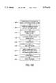
- FIG. 13Ais a process flow diagram showing the steps of the present invention used to manufacture an enclosed transceiver.
- FIG. 13Bis a process flow diagram showing the steps of the present invention used to manufacture another enclosed transceiver.
- FIG. 1A and FIG. 1Bare functional block diagrams of enclosed transceivers of the present invention.
- Enclosed transceiver 1includes a pair of batteries 2 and 3, a dipole antenna 4 and 5, and an integrated circuit (IC) 11.
- Batteries 2 and 3are in series connection through line 6 and cooperate as powering means for supplying power to IC 11 through lines 8 and 9. As will be discussed below, the series connection of two batteries simplifies conductor patterns in the enclosure.
- IC 11is a four terminal device operating as communicating means for transmitting and receiving radio signals.
- Dipole antenna 4 and 5couples radio signals between IC 11 and the communications medium which separates enclosed transceiver 11 from an interrogator, not shown. The interrogator is located up to 400 feet from enclosed transceiver 11.
- Integrated circuit 11is a transceiver including wake-up circuit 12, receiver 13, transmitter 14, control logic 15, and memory 16. Each of these functional circuits receives power signals VCC and GND on lines 8 and 9. When a received signal has substantial in-band energy as detected by wake-up circuit 12, control logic 15 enables receiver 13 for receiving and decoding a radio signal on antenna 4 and 5. Received data is provided by receiver 13 to control logic 15. Control logic 15 writes received data into memory 16. Control logic 15 also processes (i.e. decodes, tests, or edits) the received data with data stored in memory 16 and determines whether a response transmission is appropriate and the content of such a response.
- control logic 15reads transmit data from memory 16 and enables transmitter 14 for sending the transmit data as a second radio signal on antenna 4 and 5.
- Control logic 15operates as a controller for reading data from and writing data to memory 16.
- Antenna 4 and 5matches the medium to the receiver and to the transmitter for improved receiver sensitivity, and reduced transmission losses.
- Dipole antenna 4 and 5has a toroidal antenna pattern with a null along the axis of the toroid.
- FIG. 1Bis a functional block diagram of an alternate enclosed transceiver of the present invention. Like numbered elements correspond to elements already described with reference to FIG. 1A.
- Enclosed transceiver 18includes loop antenna 19, battery 20, and integrated circuit 21. Loop antenna 19 provides near omnidirectional communication capability as will be discussed with reference to FIG. 11.
- Integrated circuit 21is a three terminal device providing the same functions as integrated circuit 11 already described with reference to FIG. 1A.
- an airline agent or postal workeroperates an interrogator.
- the interrogatortransmits information to receiver 13 via an RF communication link concerning data such as the owner's name, an ID number, point of origin, weight, size, route, destination, amount of postage prepaid, billing information for debit, postage, handling, or storage costs due, time stamp, and the like.
- This received datais coupled to control logic 15 for processing, encoding, and storage in memory 16.
- Stored datais made available for call up by an interrogator at one or more points along the shipment route.
- an interrogatorupon reaching a point of shipment destination, an interrogator calls up stored data and uses it at the point of destination for insuring that the item of luggage or shipment is most assuredly and efficiently put in the hands of the desired receiver at the earliest possible time.
- an interrogator at the destination pointsends interrogation signals to the enclosed transceiver 1 where they are received by antenna 4 and 5 and first processed by sleep/wake up circuit 12.
- Wake-up circuit 12operates to bring integrated circuit 11 out of a "sleep" mode into a "waked” mode wherein receiver 13 receives and decodes signals to provide received data to control logic 15.
- control logic 15With integrated circuit 11 now in "waked" mode, memory 16 is read by control logic 15 to call-up transmit data, i.e. the above six pieces of information relating to the shipped article. Control logic 15 then couples the transmit data to transmitter 14 and enables transmitter 14 for sending transmit data to the interrogator.
- Receiver 13 and transmitter 14preferably employ one of the well known spread spectrum modulation techniques including for example: (1) direct sequencing, (2) frequency hopping, (3) pulsed FM or chirped modulation, (4) time hopping, or (5) time-frequency hopping used with pulse amplitude modulation, simple amplitude modulation or binary phase shift keying.
- spread spectrum modulation techniquesincluding for example: (1) direct sequencing, (2) frequency hopping, (3) pulsed FM or chirped modulation, (4) time hopping, or (5) time-frequency hopping used with pulse amplitude modulation, simple amplitude modulation or binary phase shift keying.
- the communication circuitry of an interrogator(not shown) is designed to conform to the modulation technique, message encoding, and modes of operation described for the enclosed transceivers of the present invention. Interrogator design is understood by those skilled in the art and, therefore, is not described herein.
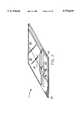
- FIG. 2is a perspective view of an enclosed transceiver as shown in FIG. 1A.
- Enclosed transceiver 1includes a base support layer 30 upon which an integrated circuit 32 is disposed on the near end of layer 30 and connected to a dipole antenna consisting of a pair of conductive strips 34 and 36 extending laterally from IC 32. These conductive strips 34 and 36 will typically be screen printed on the upper surface of base support layer 30.
- a pair of rectangularly shaped batteries 38 and 40are positioned as shown adjacent to IC 32 and are also disposed on the upper surface of base support member 30. Rectangular batteries 38 and 40 are electrically connected in series to power IC 32 in a manner more particularly described below. Assembly of enclosed transceiver 1 is completed by the folding over of an outer or upper cover member 42 which is sealed to the exposed edge surface portions of the base member 30 to thereby provide an hermetically sealed and completed package. When cover member 42 is folded over onto base member 30, conductive strip 50 is attached to batteries 38 and 40 using conductive epoxy. Conductive strip 50 provides means for coupling a pole of battery 38 to a pole of battery 40; thus accomplishing the series electrical connection of batteries 38 and 40.
- Integrated circuit 32has transmitter, memory, control logic, and receiver stages therein and is powered by batteries 38 and 40 during the transmission and reception of data to and from an interrogator to provide the interrogator with the various above information and identification parameters concerning the article, animal or person to which the enclosed transceiver is attached.
- FIG. 3is a plan view showing the conductive patterns on the base and cover members used in FIG. 2, including dotted line outlines of the locations for the IC and batteries.
- base 30 and cover 42are joined at an intersecting line 44.
- Dipole antenna strips 34 and 36are shown positioned on each side of IC 32.
- Two conductive strips 46 and 48serve to connect the bottoms of batteries 38 and 40 to IC 32.
- Conductive strip 50is provided on the upwardly facing inside surface of top cover 42, so that, when cover 42 is folded at intersecting line 44, the outer boundary 52 of cover 42 is ready to be sealed with the outer boundary 54 of base support member 30. Simultaneously, conductive strip 50 bonded by the conductive epoxy to batteries 38 and 40, completes the series electrical connection used to connect batteries 38 and 40 in series with each other and further in series circuit with integrated circuit 32 through conductive strips 46 and 48.
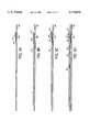
- FIG. 4A through FIG. 4Dare cross sectional views taken along lines 4--4 of FIG. 3 showing four processing steps used in constructing the enclosed transceiver shown in FIG. 3.
- FIG. 4Ashows in cross sectional view IC 32 bonded to base support member 30 by means of a spot or button of conductive epoxy material 56.
- Conductive strip 48is shown in cross section on the upper surface of base support member 30.
- battery 40is aligned in place as indicated earlier in FIG. 2 and has the right hand end thereof bonded and connected to the upper surface of conductive strip 48 by means of a spot of conductive epoxy applied to the upper surface of conductive strip 48, but not numbered in this figure.
- a stiffener material 58is applied as shown over the upper and side surfaces of IC 32.
- the stiffener materialwill preferably be an insulating material such as "glob-top" epoxy to provide a desired degree of stiffness to the package as completed.
- a spot of conductive epoxyis applied to each end of conductive strip 50, and then cover layer material 42 with the conductive epoxy thereon is folded over onto batteries 38 and 40 and base member 30 to cure and heat seal and, thus, complete and seal the package in the configuration shown in FIG. 4D.
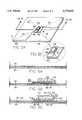
- FIG. 5Ais a perspective view of an alternate embodiment of the invention wherein the IC is mounted on a parallel plate capacitor which in turn is mounted on a battery.
- FIG. 5Bis an enlarged portion of FIG. 5A.
- the enclosed transceiver shownincludes the combination of battery 60, capacitor 62, and IC 64.
- inrush current requirements for IC 64exceed the capability of battery 60 to supply surge current, for example, due to inductive coupling or battery structure, inrush current is supplied by capacitor 62.
- the structure of battery 60is in direct contact with the upper surface 66 of a base support member 68.
- the structure of parallel plate capacitor 62is positioned intermediate to the upper surface of the structure of battery 60 and the bottom surface of IC 64.
- an exposed capacitor bottom plate area 65is provided on the left hand side of this structure and an exposed battery bottom plate area 67 is provided on the right hand side of the battery-capacitor-chip structure.
- a plurality of antenna lines 70, 72, 74, and 76form two dipole antennas connected to opposite corners of IC 64 in a generally X-shaped configuration and extend as shown from IC 64 to the four corners of the package.
- Upper polymer cover 77is sealed in place as shown to hermetically seal all of the previously identified elements of the package between base support member 68 and polymer cover 77.
- FIG. 6A through FIG. 6Eare cross sectional views taken along lines 6--6 of FIG. 5 showing five processing steps used in constructing the embodiment shown in FIG. 5.
- Base starting materialincludes a first or base polymer layer 78, such as polyester or polyethylene, which is laminated with a relatively impermeable material such as metal film, PVDC, or silicon nitride.
- Base layer 78is coated on the bottom surface thereof with a suitable adhesive film 80 which will be used for the device adhesion during device usage. If the adhesive is sufficiently impermeable, the impermeable coating may be omitted.
- the battery connection and attachmentare made on the upper surface of base layer 78 using a spot of conductive epoxy. Conductive epoxy is also used at interface 94 between battery 60 and capacitor 62 and interface 98 between capacitor 62 and IC 64.
- a thin film battery consisting of parallel plates 84 and 86is placed on base layer 78.
- a capacitor comprising parallel plates 90 and 92is attached onto battery layer 84 using a conductive epoxy.
- Bottom plate 92 of capacitor 62is somewhat larger in lateral extent than top capacitor plate 90 in order to facilitate the necessary electrical connection of battery 60 and capacitor 62 to integrated circuit 96.
- IC 96corresponds to IC 64 in FIGS. 5A and 5B.
- IC 96is then attached to top capacitor plate 90 with a conductive epoxy at interface 98, thereby providing an electrical connection.
- the bottom surface of IC 96is metallized to facilitate this connection.
- an epoxy cure heat step or metallization anneal stepis used to enhance the sealing between the various above stacked elements.
- prefabricated insulating layer 100is now laid over the battery/capacitor/IC stack in the geometry shown.
- Layer 100includes openings 102, 104, 110, and 112 therein for receiving a conductive polymer material as will be described below in the following stage of the process.
- Prefabricated holes 102, 104, 110, and 112 in layer 100are aligned, respectively, to the battery contact, to the capacitor contact, and to the contacts on the top of IC 96.
- Layer 100is then sealed to base polymer layer 78 using, for example, a conventional heating or adhesive step.
- a conductive polymer material 108is deposited in openings 102 and 104 in the lower regions of layer 100 and extended up into the upper openings 110 and 112 of layer 100 to make electrical contact as indicated on the upper surface of IC 96.
- the shaped conductive epoxy material 108may also be preformed utilizing a stamping tool or silk screening techniques and is applied as shown over the upper surface of layer 100.
- Conductive epoxy material 108forms the innermost region of the antenna structure extending from IC 96 out in the dual dipole geometry as previously described with reference to FIGS. 5A and 5B. However, the complete antenna geometry shown in FIG. 5A is outside the lateral bounds of the fragmented cross sectional views shown in FIGS. 6A through 6E. At this point in the process, an epoxy cure heat step is optional.
- polymer insulating layer 114is formed on the upper surface of layer 100 in the geometry shown and further extends over the exposed upper surfaces of the conductive epoxy polymer antenna material 108. Layer 114 is then sealed to layer 100 using either heat or adhesive sealing. Layer 114 provides a final hermetic seal for the completed device shown in cross section in FIG. 6E.
- FIG. 7is a cross-sectional view showing an arrangement of battery and capacitor alternate to the embodiment shown in FIG. 5.
- the battery and capacitorare mounted side-by-side under the IC.
- the electrical connection for battery 118 and capacitor 120 to integrated circuit 96is provided by positioning the battery 118 and capacitor 120 in the co-planar configuration shown on the surface of base polymer layer 78.
- the bottom plate of battery 118is connected through conductive epoxy layer 128 to the top surface of IC 96.
- the bottom plate of parallel plate capacitor 120is connected through conductive epoxy layer 128 to the top surface of the IC 96.
- a small space 126is provided as shown to electrically isolate battery 118 and capacitor 120.
- conductive material 128is extended as shown between the left side opening 130 in the layer 100 and a lower opening 132 in layer 100.
- layer 114is then extended over the top surface of layer 100 in the geometry shown.
- Conductive polymer material 128extends to connect the crossed antenna structure of FIG. 5 to IC 96 shown in FIG. 7.
- FIG. 8is a perspective view of another alternate embodiment of the present invention having battery surfaces defining and performing the function of a bow-tie antenna.
- IC 138is centrally positioned as shown on the upper surface of base support member 140 and is electrically connected to two triangularly shaped batteries 142 and 144, also disposed on the upper surface of base support member 140. Batteries 142 and 144 are connected in series with IC 138 when protective cover member 146 is sealed over the top surfaces of the two batteries 142 and 144 and the IC 138 using processing steps previously described.
- the entire outer surfaces of the two batteries 142 and 144serve as a "bow tie" antenna structure for the enclosed transceiver.
- the top and bottom surfaces of batteries 142 and 144are coupled together.
- Batteries 142 and 144are connected in series with the IC 138 to provide DC operating power therefor in a manner previously described.
- the dual use of the batteries as power supplies and antenna structuresminimizes the number of terminals required to connect IC 138 into an enclosed transceiver.
- FIG. 9shows an alternate, passive device embodiment of the present invention in partially cut-away perspective view wherein the battery has been altogether eliminated and further wherein a capacitor is periodically charged from an external source in a manner described below to provide operating power to the IC.
- This embodimentis known as the passive or battery-less device embodiment, since it contains no battery therein. Instead, operating power is provided by a capacitor structure identified as component 148 located beneath IC 150. A charge on capacitor 148 is maintained by conventional RF charging circuits (not shown) on IC 150 which are energized from a remote source.
- the enclosed transceiver shown in FIG. 9includes a first loop antenna 152 for receiving RF charging signals for capacitor 148 and a dipole antenna formed of conductive strips 154 and 156 for receiving and transmitting data to and from IC 150.
- capacitor 148 and IC 150are positioned and hermetically sealed between a base cover member 157 and a top cover member 158.
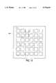
- FIG. 10is a top view of a web of enclosed transceivers of the present invention.
- Laminated sheet 200includes 36 enclosed transceivers 210 simultaneously manufactured in a plurality of cavities as already described.
- Sheet 200in a preferred embodiment includes 252 enclosed transceivers, each approximately 1.5 inches square.
- sheet 200includes one folded film as illustrated in FIGS. 2, 3, and 4; three coextensive films 114, 100, and 78 as illustrated in FIGS. 6 and 7; or two coextensive films as is apparent from FIGS. 8 and 9, and FIGS. 11 and 12 to be discussed below.
- Sheet 200in one embodiment is sectioned to obtain individual enclosed transceivers by interstitial cutting, perforation and tearing, or sheering; sectioning being simultaneous with or following the step of sealing each enclosed cavity by lamination, embossing, hot stamping or the like.
- enclosed transceiversare manufactured in a continuous strip, for example, one enclosure.
- a large number of finished devices, or websare stored on a take-up reel (not shown) supporting a corresponding large plurality of the devices.
- storage on a take-up reelnot only makes the present process conducive to high speed automated manufacturing, but in addition makes the process compatible to high speed manual or automated product dispensing and use.
- Large numbers of enclosed transceiversmay be supplied easily to a user in a conventional tape and reel format. The user can readily detatch one device at a time for immediate attaching to an article. Alternatively, enclosed transceivers a remanufactured and shipped in sheets and later sectioned by the customer.
- devicesare cut from the tape or sheet from which they were manufactured and then removably mounted on a backing.
- the backingin one embodiment is in tape format and in another equivalent embodiment is in sheet format.
- enclosed transceiversare more effectively stored in a cache for dispensing individually.
- the cachenot shown, includes means for dispensing (i.e. separately providing a transceiver on demand) and shielding means for preventing signal reception by enclosed transceivers within the cache. If shielding were not included, a supply of transceivers located within communicating range of an interrogator would soon expend battery capacity by processing signals including, for example, wake-up signals.
- Means for dispensingincludes, for example, mechanical devices for feeding a tape or sheet through an opening and mechanical devices for separating shielding materials from a tape or sheet.
- the former dispensing meansin one embodiment of the cache, cooperates with shielding across the opening including conductive rollers, separating brushes, separating fingers, and the like.
- the latter dispensing meansin another embodiment of the cache, cooperates with conductive backing material, or conductive foam as a backing or cover layer arranged to shield the exposed edges of a roll containing transceivers.
- FIG. 11is an exploded perspective view of the top and bottom films used to construct one of the enclosed transceivers shown in FIG. 10.
- the embodiment showncorresponds to enclosed transceiver 18 shown in FIG. 1B.
- Top film 214includes area 222 for lamination onto the top surface (pole) of battery 20; strip 218 for loop antenna 19; and, contact area 226.
- Each of these three featuresin a preferred embodiment, is formed of conductive ink. In an alternate and equivalent embodiment, these three features are formed of conductive epoxy.
- Bottom film 230includes area 238 for lamination onto the bottom surface (pole) of battery 20; strip 234 for loop antenna 19; contact area 254; and contact points 242, 246, and 250 for connecting integrated circuit 21 to the battery and antenna.
- Each of these six features, in a preferred embodimentis formed of conductive ink, though conductive epoxy is equivalent.
- Contact 246is intentionally misaligned with respect to area 222 to prevent shorting battery 20. However, strips 218 and 234 are aligned to coincide, as are contact areas 226 and 254, respectively. These strips and contact areas when joined by lamination cooperate as means for coupling power from battery 20 to IC 21 and, simultaneously, for electrically matching IC 21 to the communications medium by forming loop antenna 19. Thus, contacts 242, 246, and 250 correspond respectively to lines 24, 23, and 22 shown in FIG. 1B.
- the combined loop antenna and battery structureis also preferred over the dipole in that the combination provides an antenna pattern that is less subject to variation over a broad range of frequencies.
- FIG. 12is a cross-sectional view taken along lines 12--12 of FIG. 11 showing a portion of the web shown in FIG. 10 and illustrating electrical coupling to and between the films.
- the completed assemblyincludes similarly numbered elements already discussed with reference to FIG. 11.
- IC 390is prepared for assembly by forming conductive bumps 306 and 314 to terminals on its lower surface.
- bumpsare formed of conductive epoxy.
- metallic bumps, such as gold,are formed by conventional integrated circuit processes.
- IC 390 as shownis in a "flip chip" packaging orientation having substantially all circuitry formed on the surface facing film 230. Prior to assembly, a puddle of conductive epoxy is applied to contacts 250 and 242.
- IC 390is then located atop contacts 250 and 242 so that bumps 306 and 314 are surrounded within puddles 302 and 310.
- the filmis then heated to set all conductive epoxy including puddles 302 and 310, as well as strips and areas including the antenna and contact areas 226 and 254, formed of conductive epoxy.
- top film 214is aligned over bottom film 230 so that contact areas 226 and 254 are pressed together.
- FIG. 13Ais a process flow diagram showing the steps of the present invention used to manufacture an enclosed transceiver of the type shown in FIGS. 10-12.
- the manufacturing processbegins with a polyester film used for the bottom and for the top.
- Material for the bottom in a first embodimentis identical to the top and includes film with dimensional stability, for example, polyester film that has been heat stabilized or pre-shrunk.
- film with dimensional stabilityfor example, polyester film that has been heat stabilized or pre-shrunk.
- These materials, though inexpensive,are porous to substances that degrade the life and functions of the battery and integrated circuit. This disadvantage is resolved in a preferred embodiment by coating the outer surfaces of the material used for the top and bottom film with a barrier material
- barrier materialsuch as a silicon nitride deposit
- CVDchemical vapor deposition
- the depositprovides a hermetic barrier to prevent water vapor and other contaminants from affecting (e.g. oxidizing) battery and transceiver components.
- the resulting thickness of the depositis from 400 to 10,000 angstroms.
- coating on both sides of the filmprevents pin holes in each deposit from aligning in a way that defeats hermeticity.
- the thickness of the deposit and the manner of formationare design choices based on the selection of materials for the film and the deposit, as well as the system requirements for hermeticity over time.
- an alternate and equivalent embodimentuses other barrier materials including silicon oxide and silicon nitride deposited at a thickness of 100 to 400 angstroms.
- the barrier materialis formed in such an embodiment using one of the processes including evaporation deposition, chemical vapor deposition, and plasma enhanced chemical vapor deposition.
- a nitride filmis sputtered on the outside portion of a top and bottom base support layer.
- Each base support layerpreferably comprises a polymer material such as a polyester film that is laminated with a barrier layer material such as polyethylene and/or polyvinylidenechloride (PVDC). Formation of the barrier material deposit can be deferred until the enclosed transceiver is encapsulated, provided that environmental concerns such as contamination, over heating, and changes in pressure are addressed.
- PVDCpolyvinylidenechloride
- a laminate adhesiveis applied to the inner surfaces of the top and bottom films.
- the laminate adhesiveis activated in a later manufacturing step to cause the top and bottom layers to adhere.
- the adhesiveis tack free at room temperature and selected to match laminating equipment heat and pressure capabilities.
- butyl acrylateis extruded onto the films to cover the entire inside surface of each film.
- the adhesiveis screen printed for economy.
- conductorsare screen printed onto the films.
- the conductorsare formed on top of laminate adhesive. Areas such as grid conductors 222 and 238 shown in FIG. 11 for contacting the battery are, consequently, interspersed with areas of exposed laminate adhesive to provide a more durable enclosure.
- a polymer thick film inkis employed. High conductivity is provided by such inks that include copper or silver constituents. The ink preferably provides a stable surface for electrical butt contact formations. A low oxidation rate at storage temperature is desirable, though oxidation could be minimal in a controlled manufacturing environment.
- Printed circuits on the top layerare arranged to perform multiple functions when the top and bottom layers are joined.
- a conductor on the top layercompletes series or parallel circuits for devices having contacts in two planes.
- Conductor 50 in FIG. 2is one example.
- a conductor on the top layercompletes an antenna structure for the transceiver integrated circuit, as illustrated in FIG. 8.
- Third, a single conductor in the top layeraccomplishes both the first and second functions. See, for example, the conductor in FIG. 11 identified as areas 226, 222, and 218.
- conductorsare formed in a subtractive process, for example, chemical etching.
- a positive screen print processenergy and material are conserved.
- Printed circuit technologyis applied in another embodiment wherein the step of attaching the integrated circuit and the battery to a base material includes soldering and brazing.
- the base material in such an embodimentis one of a wide variety of printed circuit materials including polyimide and glass-epoxy materials.
- step 440the top and bottom base support layers are cut from the roll or web to form sheets as illustrated in FIG. 10 to facilitate use of automated component placement machinery.
- Each sheetis attached, in step 450, to a carrier panel for compatibility with conveyor based manufacturing facilities.
- step 460a carrier with sheet attached is loaded into a magazine or placed onto a conveyor for automated manufacturing. Steps 440-460, in an alternate embodiment of the manufacturing process of the present invention, are omitted as unnecessary when continuous manufacturing from roll stock is desirable.
- step 470those portions of conductors that are to make electrical contact with the integrated circuit are prepared with a coating or puddle of conductive epoxy.
- conductive epoxyIn a preferred embodiment, silver filled epoxy is employed that remains wet at room temperature until thermally cured. Application of the epoxy is by screen printing. In an alternate embodiment, epoxy is applied by dispensing.
- step 480integrated circuit die are placed so that epoxy bumps previously formed on the integrated circuit enter the puddles formed in step seven.
- the arrangement of the integrated circuit face down on the bottom filmis commonly referred to as "flip-chip" orientation.
- integrated circuitsare also placed in contact puddles formed on the top, i.e. cover layer. All die on the sheet are placed and aligned in this step 480 prior to proceeding with subsequent cure.
- step 490a batch of panels is heated to set the epoxy applied in step seven.
- a conveyor based ovensupports continuous curing. Curing temperature and duration are design choices that match the epoxy curing requirements. In a preferred embodiment, curing is performed at 150 degrees Celsius for 3 to 5 minutes. The cure is selected so as not to interfere with the characteristics of the laminate adhesive applied in step 420.
- an encapsulation materialcommonly called “glob top epoxy” is applied over the integrated circuit.
- Suitable nonconductive materialsinclude those providing a stiffening property to protect the integrated circuit and the electrical connections thereto from mechanical damage.
- the encapsulating materialis cured.
- the encapsulating materialis cured with ultraviolet radiation.
- An alternate and equivalent embodimentemploys a thermal curing process. The ultraviolet cure is preferred for rapid manufacturing.
- use of a thermal cure in step 510may permit use of a partial thermal cure in step 490, later perfected by additional thermal cure duration provided in step 510.
- step 520the battery or batteries are aligned and placed on the base support film.
- connectionis made using conductive tape having adhesive on both sides of the tape.
- Such tapecommonly includes conductive particles in the adhesive.
- the top or cover filmis aligned over the bottom or base film.
- the top filmis folded over the base film.
- the base film and top filmare aligned for continuous lamination.
- step 540the top cover film is pressed onto the bottom base film and heat is applied to activate the adhesive applied in step 420.
- the adhesive applied in step 420For butyl acrylate adhesive a temperature of from 95 to 110 degrees Celsius is preferred.
- the seal provided by automated lamination equipmentmay be incomplete or have weaknesses caused, for example, by insufficient heat or pressure at a point in an area to be sealed. Enclosing components of varying thicknesses can result in air pockets surrounding such components that, if too near the periphery, can also lead to weaknesses and voids.
- the preferred processincludes step 550 wherein the periphery of each transceiver on a sheet is subject to a second application of heat and pressure for activating laminate adhesive applied in step 420.
- the additional heat and pressure in such a localized peripherycan deform the films to form minute bosses.
- the stepis called embossing.
- the aspect of the effective application of heat and pressureis more important than the extent of consequential deformation.
- each enclosureis evacuated.
- Lamination for such an embodimentis conducted in an evacuated environment.
- Embossing in yet another embodimentis also conducted in an evacuated environment.
- step 540the circuitry of the battery powered transceiver is active by virtue of the completed circuits formed when the top cover layer is aligned and butt contacts are formed with components and the base layer. Functional tests of multiple or individual transceivers are now feasible.
- transceiversare functionally tested.
- a pair of grounded plates with surface featuresare placed on both sides of a sheet of enclosed transceivers so that each transceiver operates inside a shielded cavity.
- the wavelength used for testingis selected such that leakage through the thickness of the embossed seal is negligible. Plates similar to the embossing die used in step 550 are used in one embodiment.
- Each cavityincludes an antenna for transmitting stimulus signals and for receiving response signals for measuring the quality of each transceiver. Measurements include, for example, receiver sensitivity, transmitted spectrum, message handling capability, self-testing, and response timing.
- step 570the sheet of tested transceivers is sheered in two dimensions to singulate or separate the transceivers from one another.
- a backing materialis applied to one side of the sheet prior to singulation. Singulation for this embodiment is accomplished by kiss cutting through the top and base films leaving the transceivers attached to the backing material. Transceivers, whether attached to the backing or loose are then sorted based on the results of functional testing performed in step 560 and additional testing as needed.
- FIG. 13Bis a process flow diagram showing the steps of the present invention used to manufacture another enclosed transceiver of the types shown in FIGS. 2-9.
- This embodiment of the method of the present inventionincludes nine (9) processing steps or fabrication stages which are used in the overall manufacturing process and in the construction of an enclosed transceiver.
- a circuit patternis initially formed on a base layer material.
- This base layer materialis preferably a polymer such as a polyester film that is laminated with a barrier layer material such as polyethylene and/or polyvinylidenechloride (PVDC).
- PVDCpolyvinylidenechloride
- the circuit patternis cured and a conductive epoxy material is applied.
- an integrated circuit chipis aligned onto the base layer.
- two (2) batteriesare aligned onto the base layer. In an alternate enclosed transceiver, the batteries are stacked vertically in either a series or parallel electrical connection.
- the epoxy applied in step 612is cured.
- a stiffener materialis applied.
- step 622epoxy is applied to the top surface of the battery and then the top half of the base layer is folded over the bottom half so that the top half forms the top cover.
- step 624the epoxy material applied in step 622 is cured.
- step 626the package is sealed to complete manufacturing of the package.
- an enclosed transceiver used as an RFID devicehas utility directed to a wide variety of applications including, but not limited to, airline baggage (luggage, freight, and mail); parcel post (Federal Express and United Parcel Service); U.S. Mail; manufacturing; inventory; personnel security.
- a "sticker”refers generally to a label, tag, marker, stamp, identifier, packing slip, invoice, package seal, tape, band, clasp, medallion, emblem, shield, and escutcheon regardless of printed or handwritten material thereon.
- Mechanical coupling of a "sticker" so defined to an article, person, plant, or animalis not restricted to adhesive but is intended to broadly include all forms of fastening, tieing, and securing.
Landscapes
- Engineering & Computer Science (AREA)
- Computer Networks & Wireless Communication (AREA)
- Radar, Positioning & Navigation (AREA)
- Computer Hardware Design (AREA)
- Remote Sensing (AREA)
- Microelectronics & Electronic Packaging (AREA)
- Physics & Mathematics (AREA)
- General Physics & Mathematics (AREA)
- Signal Processing (AREA)
- Theoretical Computer Science (AREA)
- Power Engineering (AREA)
- Computer Security & Cryptography (AREA)
- General Engineering & Computer Science (AREA)
- Credit Cards Or The Like (AREA)
Abstract
Description
Claims (10)
Priority Applications (3)
| Application Number | Priority Date | Filing Date | Title |
|---|---|---|---|
| US08/947,681US5779839A (en) | 1992-06-17 | 1997-09-26 | Method of manufacturing an enclosed transceiver |
| US09/115,492US6045652A (en) | 1992-06-17 | 1998-07-14 | Method of manufacturing an enclosed transceiver |
| US09/542,625US6375780B1 (en) | 1992-06-17 | 2000-04-04 | Method of manufacturing an enclosed transceiver |
Applications Claiming Priority (9)
| Application Number | Priority Date | Filing Date | Title |
|---|---|---|---|
| US89977792A | 1992-06-17 | 1992-06-17 | |
| US92889992A | 1992-08-12 | 1992-08-12 | |
| US08/008,529US5326652A (en) | 1993-01-25 | 1993-01-25 | Battery package and method using flexible polymer films having a deposited layer of an inorganic material |
| US08/123,030US5448110A (en) | 1992-06-17 | 1993-09-14 | Enclosed transceiver |
| US13767793A | 1993-10-14 | 1993-10-14 | |
| US08/168,909US5497140A (en) | 1992-08-12 | 1993-12-17 | Electrically powered postage stamp or mailing or shipping label operative with radio frequency (RF) communication |
| US48918595A | 1995-06-09 | 1995-06-09 | |
| US60268696A | 1996-02-16 | 1996-02-16 | |
| US08/947,681US5779839A (en) | 1992-06-17 | 1997-09-26 | Method of manufacturing an enclosed transceiver |
Related Parent Applications (4)
| Application Number | Title | Priority Date | Filing Date |
|---|---|---|---|
| US08/008,529ContinuationUS5326652A (en) | 1992-06-17 | 1993-01-25 | Battery package and method using flexible polymer films having a deposited layer of an inorganic material |
| US08/168,909Continuation-In-PartUS5497140A (en) | 1992-05-15 | 1993-12-17 | Electrically powered postage stamp or mailing or shipping label operative with radio frequency (RF) communication |
| US48918595AContinuation-In-Part | 1992-05-15 | 1995-06-09 | |
| US60268696AContinuation | 1992-06-17 | 1996-02-16 |
Related Child Applications (1)
| Application Number | Title | Priority Date | Filing Date |
|---|---|---|---|
| US09/115,492DivisionUS6045652A (en) | 1992-06-17 | 1998-07-14 | Method of manufacturing an enclosed transceiver |
Publications (1)
| Publication Number | Publication Date |
|---|---|
| US5779839Atrue US5779839A (en) | 1998-07-14 |
Family
ID=27573946
Family Applications (1)
| Application Number | Title | Priority Date | Filing Date |
|---|---|---|---|
| US08/947,681Expired - LifetimeUS5779839A (en) | 1992-06-17 | 1997-09-26 | Method of manufacturing an enclosed transceiver |
Country Status (1)
| Country | Link |
|---|---|
| US (1) | US5779839A (en) |
Cited By (112)
| Publication number | Priority date | Publication date | Assignee | Title |
|---|---|---|---|---|
| US5955949A (en)* | 1997-08-18 | 1999-09-21 | X-Cyte, Inc. | Layered structure for a transponder tag |
| US5964656A (en)* | 1998-05-19 | 1999-10-12 | Meat Processing Service Corp. Inc. | Radio frequency identification device and method of use |
| US6013949A (en)* | 1992-08-12 | 2000-01-11 | Micron Technology, Inc. | Miniature Radio Frequency Transceiver |
| FR2787220A1 (en)* | 1998-12-11 | 2000-06-16 | Plasto Sa | Electronic label for marking control and identification of product has communication device that permits exchange of information between electronic label and external computer system |
| US6127928A (en)* | 1998-02-10 | 2000-10-03 | E-Tag Systems, Inc. | Method and apparatus for locating and tracking documents and other objects |
| US6147662A (en)* | 1999-09-10 | 2000-11-14 | Moore North America, Inc. | Radio frequency identification tags and labels |
| US6166638A (en)* | 1998-04-03 | 2000-12-26 | Intermec Ip Corp. | RF/ID transponder with squinted beam radiation pattern using dipole-over-ground plane antenna |
| US6196912B1 (en)* | 1998-05-19 | 2001-03-06 | Meat Processing Service Corporation | Machine readable tag |
| US6248199B1 (en) | 1999-04-26 | 2001-06-19 | Soundcraft, Inc. | Method for the continuous fabrication of access control and identification cards with embedded electronics or other elements |
| US6273339B1 (en) | 1999-08-30 | 2001-08-14 | Micron Technology, Inc. | Tamper resistant smart card and method of protecting data in a smart card |
| WO2001078002A1 (en)* | 2000-04-06 | 2001-10-18 | Schreiner Gmbh & Co. Kg | Data exchange label and a method for applying the same |
| WO2001075772A3 (en)* | 2000-04-04 | 2002-03-28 | Smartag S Pte Ltd | Method for manufacturing of rfid inlet |
| US6375780B1 (en)* | 1992-06-17 | 2002-04-23 | Micron Technology, Inc. | Method of manufacturing an enclosed transceiver |
| WO2002029929A3 (en)* | 2000-10-03 | 2002-07-18 | Marconi Corp Plc | Multi-band wireless communication device |
| US6469627B1 (en) | 2000-02-11 | 2002-10-22 | Marconi Communications Inc. | Mounting clip having a wireless communication device |
| US20020167500A1 (en)* | 1998-09-11 | 2002-11-14 | Visible Techknowledgy, Llc | Smart electronic label employing electronic ink |
| US20020167407A1 (en)* | 1999-12-07 | 2002-11-14 | Manfred Fries | Product label, method of producing product labels and method for identifying products in a contactless and forgery-proof manner |
| US6509217B1 (en) | 1999-10-22 | 2003-01-21 | Damoder Reddy | Inexpensive, reliable, planar RFID tag structure and method for making same |
| US6580357B1 (en) | 2000-02-11 | 2003-06-17 | Marconi Communications Inc. | Handle tag for identification of a container |
| EP1136945A4 (en)* | 1998-11-30 | 2003-07-16 | Hitachi Ltd | METHOD FOR MOUNTING AN ELECTRONIC CIRCUIT CHIP |
| WO2003061095A1 (en)* | 2002-01-02 | 2003-07-24 | International Business Machines Corporation | System level battery integration system |
| US6648232B1 (en) | 2000-10-24 | 2003-11-18 | Moore North America, Inc. | High temperature tag having enclosed transceiver |
| WO2003043101A3 (en)* | 2001-11-16 | 2003-12-04 | Giesecke & Devrient Gmbh | Film battery for portable data carriers having an antenna function |
| US20040041714A1 (en)* | 2002-05-07 | 2004-03-04 | Forster Ian J. | RFID temperature device and method |
| US20040041709A1 (en)* | 2002-05-23 | 2004-03-04 | Forster Ian J. | Device and method for identifying a containers |
| US6720865B1 (en) | 2000-02-11 | 2004-04-13 | Marconi Intellectual Property (Us) | Resilient member with wireless communication device |
| US6727803B2 (en) | 2001-03-16 | 2004-04-27 | E-Tag Systems, Inc. | Method and apparatus for efficiently querying and identifying multiple items on a communication channel |
| US6753830B2 (en) | 1998-09-11 | 2004-06-22 | Visible Tech-Knowledgy, Inc. | Smart electronic label employing electronic ink |
| US20040132406A1 (en)* | 2003-01-03 | 2004-07-08 | Scott Jeff W. | Tags, wireless communication systems, tag communication methods, and wireless communications methods |
| US6774766B1 (en) | 2000-07-21 | 2004-08-10 | E-Tag Systems, Inc. | Method for efficiently querying and identifying multiple items on a communication channel |
| US6778088B1 (en)* | 2000-02-11 | 2004-08-17 | Marconi Intellectual Property (Us) Inc. | Deployable identification device |
| US20040183182A1 (en)* | 2002-01-23 | 2004-09-23 | Susan Swindlehurst | Apparatus incorporating small-feature-size and large-feature-size components and method for making same |
| US6816380B2 (en) | 2001-05-31 | 2004-11-09 | Alien Technology Corporation | Electronic devices with small functional elements supported on a carrier |
| US20040238623A1 (en)* | 2003-05-09 | 2004-12-02 | Wayne Asp | Component handling device having a film insert molded RFID tag |
| US20040246099A1 (en)* | 1992-08-12 | 2004-12-09 | Micron Technology, Inc. | Miniature radio frequency transceiver |
| US20050077604A1 (en)* | 2003-10-13 | 2005-04-14 | Mccain Joseph Harry | Integrated circuit package with laminated power cell having coplanar electrode |
| US6924781B1 (en) | 1998-09-11 | 2005-08-02 | Visible Tech-Knowledgy, Inc. | Smart electronic label employing electronic ink |
| US20050174258A1 (en)* | 2002-06-24 | 2005-08-11 | Kazuki Yamanouchi | Gate management system and method for vehicle passage gate |
| US20050238455A1 (en)* | 2004-04-23 | 2005-10-27 | Toteff Thomas S | Dual purpose track for holding wheel chocks and strap clips to tie down dirt bikes to trailers |
| US20050260492A1 (en)* | 2004-04-21 | 2005-11-24 | Tucholski Gary R | Thin printable flexible electrochemical cell and method of making the same |
| US20060032926A1 (en)* | 2004-08-13 | 2006-02-16 | Fujitsu Limited | Radio frequency identification (RFID) tag and manufacturing method thereof |
| US20060092025A1 (en)* | 2004-11-02 | 2006-05-04 | Michael Fein | Variation of conductive cross section and/or material to enhance performance and/or reduce material consumption of electronic assemblies |
| US20060109123A1 (en)* | 2004-11-22 | 2006-05-25 | Curt Carrender | Radio frequency identification (RFID) tag for an item having a conductive layer included or attached |
| US20060164213A1 (en)* | 2005-01-26 | 2006-07-27 | Battelle Memorial Institute | Method for autonomous establishment and utilization of an active-RF tag network |
| US20060176179A1 (en)* | 2005-01-26 | 2006-08-10 | Battelle Memorial Institute | Bendable, active radio-frequency sensor tags and a system of same |
| US20060267778A1 (en)* | 2003-03-24 | 2006-11-30 | Gengel Gleen W | RFID tags and processes for producing RFID tags |
| US20060267167A1 (en)* | 2004-10-25 | 2006-11-30 | Mccain Joseph H | Microelectronic device with integrated energy source |
| US20060283932A1 (en)* | 2005-04-08 | 2006-12-21 | Wayne Asp | Identification tag for fluid containment drum |
| US20070031992A1 (en)* | 2005-08-05 | 2007-02-08 | Schatz Kenneth D | Apparatuses and methods facilitating functional block deposition |
| US20070128940A1 (en)* | 2003-12-08 | 2007-06-07 | Cochlear Limited | Cochlear implant assembly |
| US7288432B2 (en) | 1999-03-16 | 2007-10-30 | Alien Technology Corporation | Electronic devices with small functional elements supported on a carrier |
| US20070271467A1 (en)* | 1997-08-10 | 2007-11-22 | Gemplus | Method for making smart cards capable of operating with and without contact |
| USRE40137E1 (en) | 1997-05-01 | 2008-03-04 | Micron Technology, Inc. | Methods for forming integrated circuits within substrates |
| US7353598B2 (en) | 2004-11-08 | 2008-04-08 | Alien Technology Corporation | Assembly comprising functional devices and method of making same |
| US7385284B2 (en) | 2004-11-22 | 2008-06-10 | Alien Technology Corporation | Transponder incorporated into an electronic device |
| US7452748B1 (en) | 2004-11-08 | 2008-11-18 | Alien Technology Corporation | Strap assembly comprising functional block deposited therein and method of making same |
| US20090035522A1 (en)* | 2007-07-31 | 2009-02-05 | Smith Gilbert G | Forming electrically isolated conductive traces |
| US20090038746A1 (en)* | 2005-05-06 | 2009-02-12 | Tucholski Gary R | Rfid antenna-battery assembly and the method to make the same |
| US7542301B1 (en) | 2005-06-22 | 2009-06-02 | Alien Technology Corporation | Creating recessed regions in a substrate and assemblies having such recessed regions |
| US7551141B1 (en) | 2004-11-08 | 2009-06-23 | Alien Technology Corporation | RFID strap capacitively coupled and method of making same |
| EP1101203B2 (en)† | 1998-07-27 | 2009-06-24 | Infineon Technologies AG | Security paper, method and device for checking the authenticity of documents recorded thereon |
| CN100561507C (en)* | 2006-05-23 | 2009-11-18 | 智威科技股份有限公司 | RFID package structure |
| US20100090655A1 (en)* | 2008-10-08 | 2010-04-15 | Keating Joseph A | Environmentally-Powered Wireless Sensor Module |
| US20100115572A1 (en)* | 2008-11-05 | 2010-05-06 | Comcast Cable Communications, Llc | System and method for providing digital content |
| US7791489B2 (en) | 2003-09-03 | 2010-09-07 | Metrologic Instruments, Inc. | Electronic-ink based RFID tag for attachment to a consumer item and displaying graphical indicia indicating whether or not said consumer items has been read and its integrated RFID module has been activated or deactivated |
| US7839285B2 (en) | 1997-08-20 | 2010-11-23 | Round Rock Resarch, LLC | Electronic communication devices, methods of forming electrical communication devices, and communications methods |
| US20100326723A1 (en)* | 2007-07-17 | 2010-12-30 | Cochlear Limited | Electrically insulative structure having holes for feedthroughs |
| US7959769B2 (en) | 2004-12-08 | 2011-06-14 | Infinite Power Solutions, Inc. | Deposition of LiCoO2 |
| US7993773B2 (en) | 2002-08-09 | 2011-08-09 | Infinite Power Solutions, Inc. | Electrochemical apparatus with barrier layer protected substrate |
| US20110211976A1 (en)* | 2010-02-26 | 2011-09-01 | Entegris, Inc. | Method and system for optimizing operation of a pump |
| US20110211975A1 (en)* | 2010-02-26 | 2011-09-01 | Entegris, Inc. | Method and system for controlling operation of a pump based on filter information in a filter information tag |
| US8021778B2 (en) | 2002-08-09 | 2011-09-20 | Infinite Power Solutions, Inc. | Electrochemical apparatus with barrier layer protected substrate |
| US8029927B2 (en) | 2005-03-22 | 2011-10-04 | Blue Spark Technologies, Inc. | Thin printable electrochemical cell utilizing a “picture frame” and methods of making the same |
| US8062708B2 (en) | 2006-09-29 | 2011-11-22 | Infinite Power Solutions, Inc. | Masking of and material constraint for depositing battery layers on flexible substrates |
| US8197781B2 (en) | 2006-11-07 | 2012-06-12 | Infinite Power Solutions, Inc. | Sputtering target of Li3PO4 and method for producing same |
| US8228193B1 (en)* | 1998-09-14 | 2012-07-24 | Tuemer Tuemay O | Tag having a semiconductor chip and method of attachment to article |
| US8234507B2 (en) | 2009-01-13 | 2012-07-31 | Metrologic Instruments, Inc. | Electronic-ink display device employing a power switching mechanism automatically responsive to predefined states of device configuration |
| US8236443B2 (en) | 2002-08-09 | 2012-08-07 | Infinite Power Solutions, Inc. | Metal film encapsulation |
| US8260203B2 (en) | 2008-09-12 | 2012-09-04 | Infinite Power Solutions, Inc. | Energy device with integral conductive surface for data communication via electromagnetic energy and method thereof |
| US8268488B2 (en) | 2007-12-21 | 2012-09-18 | Infinite Power Solutions, Inc. | Thin film electrolyte for thin film batteries |
| US8289164B2 (en) | 2003-12-12 | 2012-10-16 | Semiconductor Energy Laboratory Co., Ltd. | Semiconductor device and manufacturing method thereof |
| US8350519B2 (en) | 2008-04-02 | 2013-01-08 | Infinite Power Solutions, Inc | Passive over/under voltage control and protection for energy storage devices associated with energy harvesting |
| US8394522B2 (en) | 2002-08-09 | 2013-03-12 | Infinite Power Solutions, Inc. | Robust metal film encapsulation |
| US8404376B2 (en) | 2002-08-09 | 2013-03-26 | Infinite Power Solutions, Inc. | Metal film encapsulation |
| US8431264B2 (en) | 2002-08-09 | 2013-04-30 | Infinite Power Solutions, Inc. | Hybrid thin-film battery |
| US8441411B2 (en) | 2007-07-18 | 2013-05-14 | Blue Spark Technologies, Inc. | Integrated electronic device and methods of making the same |
| US8445130B2 (en) | 2002-08-09 | 2013-05-21 | Infinite Power Solutions, Inc. | Hybrid thin-film battery |
| US8457013B2 (en) | 2009-01-13 | 2013-06-04 | Metrologic Instruments, Inc. | Wireless dual-function network device dynamically switching and reconfiguring from a wireless network router state of operation into a wireless network coordinator state of operation in a wireless communication network |
| US8518581B2 (en) | 2008-01-11 | 2013-08-27 | Inifinite Power Solutions, Inc. | Thin film encapsulation for thin film batteries and other devices |
| US8574754B2 (en) | 2007-12-19 | 2013-11-05 | Blue Spark Technologies, Inc. | High current thin electrochemical cell and methods of making the same |
| US8599572B2 (en) | 2009-09-01 | 2013-12-03 | Infinite Power Solutions, Inc. | Printed circuit board with integrated thin film battery |
| US8636876B2 (en) | 2004-12-08 | 2014-01-28 | R. Ernest Demaray | Deposition of LiCoO2 |
| US8728285B2 (en) | 2003-05-23 | 2014-05-20 | Demaray, Llc | Transparent conductive oxides |
| US8753097B2 (en) | 2005-11-21 | 2014-06-17 | Entegris, Inc. | Method and system for high viscosity pump |
| US8765284B2 (en) | 2012-05-21 | 2014-07-01 | Blue Spark Technologies, Inc. | Multi-cell battery |
| US8906523B2 (en) | 2008-08-11 | 2014-12-09 | Infinite Power Solutions, Inc. | Energy device with integral collector surface for electromagnetic energy harvesting and method thereof |
| US9027242B2 (en) | 2011-09-22 | 2015-05-12 | Blue Spark Technologies, Inc. | Cell attachment method |
| US9297374B2 (en) | 2010-10-20 | 2016-03-29 | Entegris, Inc. | Method and system for pump priming |
| US9334557B2 (en) | 2007-12-21 | 2016-05-10 | Sapurast Research Llc | Method for sputter targets for electrolyte films |
| US9444078B2 (en) | 2012-11-27 | 2016-09-13 | Blue Spark Technologies, Inc. | Battery cell construction |
| US9634296B2 (en) | 2002-08-09 | 2017-04-25 | Sapurast Research Llc | Thin film battery on an integrated circuit or circuit board and method thereof |
| US9693689B2 (en) | 2014-12-31 | 2017-07-04 | Blue Spark Technologies, Inc. | Body temperature logging patch |
| US9782082B2 (en) | 2012-11-01 | 2017-10-10 | Blue Spark Technologies, Inc. | Body temperature logging patch |
| WO2018081522A1 (en)* | 2016-10-28 | 2018-05-03 | Avery Dennison Retail Information Services, Llc | Rfid tags designed to work on difficult substrates |
| US10680277B2 (en) | 2010-06-07 | 2020-06-09 | Sapurast Research Llc | Rechargeable, high-density electrochemical device |
| US10849501B2 (en) | 2017-08-09 | 2020-12-01 | Blue Spark Technologies, Inc. | Body temperature logging patch |
| US11058871B2 (en) | 2003-12-08 | 2021-07-13 | Cochlear Limited | Manufacturing an electrode array for a stimulating medical device |
| EP3923197A1 (en)* | 2020-06-08 | 2021-12-15 | eTEP Inc. | Packaging system with detection of product tampering and/or falsification and integrated galvanic cell(s) |
| EP4022674A2 (en)* | 2019-08-26 | 2022-07-06 | X-Celeprint Limited | Variable stiffness modules |
| WO2024220204A3 (en)* | 2023-04-19 | 2025-01-02 | Trackonomy Systems, Inc. | Wireless tracking device for air cargo containers and assets loaded onto aircraft |
| US12236397B2 (en) | 2023-02-03 | 2025-02-25 | Trackonomy Systems, Inc. | Monitoring of unit load device and carts using wireless IOT devices |
| US12363507B2 (en) | 2023-02-03 | 2025-07-15 | Trackonomy Systems, Inc. | Wireless tracking device for air cargo containers and assets loaded onto aircraft |
Citations (33)
| Publication number | Priority date | Publication date | Assignee | Title |
|---|---|---|---|---|
| US3706094A (en)* | 1970-02-26 | 1972-12-12 | Peter Harold Cole | Electronic surveillance system |
| US3750167A (en)* | 1971-07-22 | 1973-07-31 | Gen Dynamics Corp | Postal tracking system |
| US3780368A (en)* | 1970-02-20 | 1973-12-18 | Svejsecentralen | Method of marking and subsequently localizing, identifying and recording physical objects |
| US3832530A (en)* | 1972-01-04 | 1974-08-27 | Westinghouse Electric Corp | Object identifying apparatus |
| US3849633A (en)* | 1972-01-04 | 1974-11-19 | Westinghouse Electric Corp | Object identifying apparatus |
| US4049969A (en)* | 1970-03-19 | 1977-09-20 | The United States Of America As Represented By The Secretary Of The Air Force | Passive optical transponder |
| US4262631A (en)* | 1979-10-01 | 1981-04-21 | Kubacki Ronald M | Thin film deposition apparatus using an RF glow discharge |
| US4331957A (en)* | 1979-04-20 | 1982-05-25 | Bengt Enander | Transponder for use in locating avalanche victims |
| US4399441A (en)* | 1980-01-25 | 1983-08-16 | Unisearch Limited | Apparatus for remote temperature reading |
| US4418411A (en)* | 1980-03-11 | 1983-11-29 | Brown, Boveri & Cif Ag | Method and apparatus for generating an equipment reply signal for the automatic identification of objects and/or living beings |
| US4484355A (en)* | 1983-04-11 | 1984-11-20 | Ritron, Inc. | Handheld transceiver with frequency synthesizer and sub-audible tone squelch system |
| US4680724A (en)* | 1982-12-03 | 1987-07-14 | Casio Computer Co., Ltd. | Sheet-like miniaturized electronic device |
| US4727560A (en)* | 1985-05-30 | 1988-02-23 | U.S. Philips Corporation | Charge-coupled device with reduced signal distortion |
| US4746618A (en)* | 1987-08-31 | 1988-05-24 | Energy Conversion Devices, Inc. | Method of continuously forming an array of photovoltaic cells electrically connected in series |
| US4746830A (en)* | 1986-03-14 | 1988-05-24 | Holland William R | Electronic surveillance and identification |
| US4756717A (en)* | 1981-08-24 | 1988-07-12 | Polaroid Corporation | Laminar batteries and methods of making the same |
| US4777563A (en)* | 1986-05-02 | 1988-10-11 | Toshiba Battery Co., Ltd. | Thin type electronic instrument |
| US4827110A (en)* | 1987-06-11 | 1989-05-02 | Fluoroware, Inc. | Method and apparatus for monitoring the location of wafer disks |
| US4827395A (en)* | 1983-04-21 | 1989-05-02 | Intelli-Tech Corporation | Manufacturing monitoring and control systems |
| US4854328A (en)* | 1987-03-23 | 1989-08-08 | Philip Pollack | Animal monitoring telltale and information system |
| US4882294A (en)* | 1988-08-17 | 1989-11-21 | Delco Electronics Corporation | Process for forming an epitaxial layer having portions of different thicknesses |
| US4918631A (en)* | 1984-09-07 | 1990-04-17 | Casio Computer Co., Ltd. | Compact type electronic information card |
| US4942327A (en)* | 1988-06-01 | 1990-07-17 | Hitachi, Ltd. | Solid state electronic device |
| US5008776A (en)* | 1990-06-06 | 1991-04-16 | Sgs-Thomson Microelectronics, Inc. | Zero power IC module |
| US5023573A (en)* | 1989-09-21 | 1991-06-11 | Westinghouse Electric Corp. | Compact frequency selective limiter configuration |
| US5095240A (en)* | 1989-11-13 | 1992-03-10 | X-Cyte, Inc. | Inductively coupled saw device and method for making the same |
| US5148504A (en)* | 1991-10-16 | 1992-09-15 | At&T Bell Laboratories | Optical integrated circuit designed to operate by use of photons |
| US5153710A (en)* | 1991-07-26 | 1992-10-06 | Sgs-Thomson Microelectronics, Inc. | Integrated circuit package with laminated backup cell |
| US5166502A (en)* | 1990-01-05 | 1992-11-24 | Trend Plastics, Inc. | Gaming chip with implanted programmable identifier means and process for fabricating same |
| US5302954A (en)* | 1987-12-04 | 1994-04-12 | Magellan Corporation (Australia) Pty. Ltd. | Identification apparatus and methods |
| US5313211A (en)* | 1990-08-13 | 1994-05-17 | Sharp Kabushiki Kaisha | Portable data processing device capable of transmitting processed data on a radio by reflection of unmodulated carrier signal externally applied |
| US5340968A (en)* | 1991-05-07 | 1994-08-23 | Nippondenso Company, Ltd. | Information storage medium with electronic and visual areas |
| US5448110A (en)* | 1992-06-17 | 1995-09-05 | Micron Communications, Inc. | Enclosed transceiver |
- 1997
- 1997-09-26USUS08/947,681patent/US5779839A/ennot_activeExpired - Lifetime
Patent Citations (33)
| Publication number | Priority date | Publication date | Assignee | Title |
|---|---|---|---|---|
| US3780368A (en)* | 1970-02-20 | 1973-12-18 | Svejsecentralen | Method of marking and subsequently localizing, identifying and recording physical objects |
| US3706094A (en)* | 1970-02-26 | 1972-12-12 | Peter Harold Cole | Electronic surveillance system |
| US4049969A (en)* | 1970-03-19 | 1977-09-20 | The United States Of America As Represented By The Secretary Of The Air Force | Passive optical transponder |
| US3750167A (en)* | 1971-07-22 | 1973-07-31 | Gen Dynamics Corp | Postal tracking system |
| US3832530A (en)* | 1972-01-04 | 1974-08-27 | Westinghouse Electric Corp | Object identifying apparatus |
| US3849633A (en)* | 1972-01-04 | 1974-11-19 | Westinghouse Electric Corp | Object identifying apparatus |
| US4331957A (en)* | 1979-04-20 | 1982-05-25 | Bengt Enander | Transponder for use in locating avalanche victims |
| US4262631A (en)* | 1979-10-01 | 1981-04-21 | Kubacki Ronald M | Thin film deposition apparatus using an RF glow discharge |
| US4399441A (en)* | 1980-01-25 | 1983-08-16 | Unisearch Limited | Apparatus for remote temperature reading |
| US4418411A (en)* | 1980-03-11 | 1983-11-29 | Brown, Boveri & Cif Ag | Method and apparatus for generating an equipment reply signal for the automatic identification of objects and/or living beings |
| US4756717A (en)* | 1981-08-24 | 1988-07-12 | Polaroid Corporation | Laminar batteries and methods of making the same |
| US4680724A (en)* | 1982-12-03 | 1987-07-14 | Casio Computer Co., Ltd. | Sheet-like miniaturized electronic device |
| US4484355A (en)* | 1983-04-11 | 1984-11-20 | Ritron, Inc. | Handheld transceiver with frequency synthesizer and sub-audible tone squelch system |
| US4827395A (en)* | 1983-04-21 | 1989-05-02 | Intelli-Tech Corporation | Manufacturing monitoring and control systems |
| US4918631A (en)* | 1984-09-07 | 1990-04-17 | Casio Computer Co., Ltd. | Compact type electronic information card |
| US4727560A (en)* | 1985-05-30 | 1988-02-23 | U.S. Philips Corporation | Charge-coupled device with reduced signal distortion |
| US4746830A (en)* | 1986-03-14 | 1988-05-24 | Holland William R | Electronic surveillance and identification |
| US4777563A (en)* | 1986-05-02 | 1988-10-11 | Toshiba Battery Co., Ltd. | Thin type electronic instrument |
| US4854328A (en)* | 1987-03-23 | 1989-08-08 | Philip Pollack | Animal monitoring telltale and information system |
| US4827110A (en)* | 1987-06-11 | 1989-05-02 | Fluoroware, Inc. | Method and apparatus for monitoring the location of wafer disks |
| US4746618A (en)* | 1987-08-31 | 1988-05-24 | Energy Conversion Devices, Inc. | Method of continuously forming an array of photovoltaic cells electrically connected in series |
| US5302954A (en)* | 1987-12-04 | 1994-04-12 | Magellan Corporation (Australia) Pty. Ltd. | Identification apparatus and methods |
| US4942327A (en)* | 1988-06-01 | 1990-07-17 | Hitachi, Ltd. | Solid state electronic device |
| US4882294A (en)* | 1988-08-17 | 1989-11-21 | Delco Electronics Corporation | Process for forming an epitaxial layer having portions of different thicknesses |
| US5023573A (en)* | 1989-09-21 | 1991-06-11 | Westinghouse Electric Corp. | Compact frequency selective limiter configuration |
| US5095240A (en)* | 1989-11-13 | 1992-03-10 | X-Cyte, Inc. | Inductively coupled saw device and method for making the same |
| US5166502A (en)* | 1990-01-05 | 1992-11-24 | Trend Plastics, Inc. | Gaming chip with implanted programmable identifier means and process for fabricating same |
| US5008776A (en)* | 1990-06-06 | 1991-04-16 | Sgs-Thomson Microelectronics, Inc. | Zero power IC module |
| US5313211A (en)* | 1990-08-13 | 1994-05-17 | Sharp Kabushiki Kaisha | Portable data processing device capable of transmitting processed data on a radio by reflection of unmodulated carrier signal externally applied |
| US5340968A (en)* | 1991-05-07 | 1994-08-23 | Nippondenso Company, Ltd. | Information storage medium with electronic and visual areas |
| US5153710A (en)* | 1991-07-26 | 1992-10-06 | Sgs-Thomson Microelectronics, Inc. | Integrated circuit package with laminated backup cell |
| US5148504A (en)* | 1991-10-16 | 1992-09-15 | At&T Bell Laboratories | Optical integrated circuit designed to operate by use of photons |
| US5448110A (en)* | 1992-06-17 | 1995-09-05 | Micron Communications, Inc. | Enclosed transceiver |
Non-Patent Citations (24)
| Title |
|---|
| "Airco coating technology announces contracts in its toll coating program"; Mar. 26, 1993 press release from Airco Coating Technology, Fairfield, CA. |
| A. Rizika; "Vapor Coating with SiOx : The Flexible Glass Barrier"; presented Nov. 8-11, 1992 at Pack Expo '92 Conference, Chicago, Ill. |
| A. Rizika; Vapor Coating with SiO x : The Flexible Glass Barrier ; presented Nov. 8 11, 1992 at Pack Expo 92 Conference, Chicago, Ill.* |
| Airco coating technology announces contracts in its toll coating program ; Mar. 26, 1993 press release from Airco Coating Technology, Fairfield, CA.* |
| C.W. Pierce; "Epitaxy"; 1988, 1983; p.55; in VLSI Technology; S.M. Sze, editor; McGraw-Hill Book Co. |
| C.W. Pierce; Epitaxy ; 1988, 1983; p.55; in VLSI Technology; S.M. Sze, editor; McGraw Hill Book Co.* |
| J. Rice; "Silica-coated films to go commercial in '93"; from Oct. 93 issue of Food Processing. |
| J. Rice; Silica coated films to go commercial in 93 ; from Oct. 93 issue of Food Processing.* |
| J.T. Felts; "Transparent Barrier Coatings Update: Flexible Substrates"; Airco Coating Technology, Concord, CA. (Publication date not shown; mailed by Airco to Mark Tuttle Sept. 21, 1993). |
| J.T. Felts; "Transparent Gas Barrier Technologies"; Airco Coating Technology, Concord, CA. (Publication date not shown; mailed by Airco to Mark Tuttle Sep. 21, 1993). |
| J.T. Felts; Transparent Barrier Coatings Update: Flexible Substrates ; Airco Coating Technology, Concord, CA. (Publication date not shown; mailed by Airco to Mark Tuttle Sept. 21, 1993).* |
| J.T. Felts; Transparent Gas Barrier Technologies ; Airco Coating Technology, Concord, CA. (Publication date not shown; mailed by Airco to Mark Tuttle Sep. 21, 1993).* |
| Keith Casson and Kelly Habeck, "High Temperature Packaging: Flip Chip on Flexible Laminate," Jan. 1992, Surface Mount Technology pp. 19-20. |
| Keith Casson and Kelly Habeck, High Temperature Packaging: Flip Chip on Flexible Laminate, Jan. 1992, Surface Mount Technology pp. 19 20.* |
| Ken Gilleo, "Using SM Devices On Flexible Circuitry," Mar. 1986, Electri-onics, pp. 20-23. |
| Ken Gilleo, Using SM Devices On Flexible Circuitry, Mar. 1986, Electri onics, pp. 20 23.* |
| P. Ang; "Progress of QLF Barrier Coating"; Airco Coating Technology, Concord, CA. (Publication date not shown; mailed by Airco to Mark Tuttle Sept. 21, 1993). |
| P. Ang; Progress of QLF Barrier Coating ; Airco Coating Technology, Concord, CA. (Publication date not shown; mailed by Airco to Mark Tuttle Sept. 21, 1993).* |
| R. Wayne Johnson, "Polymer Thick Films: Technology and Materials," Circuits Manufacturing Jul. 1982. |
| R. Wayne Johnson, Polymer Thick Films: Technology and Materials, Circuits Manufacturing Jul. 1982.* |
| R.J. Nelson; "Plasma Enhanced Chemical Vapor Deposition of SiOx Coatings for Gas Diffusion Barrier Enhancement of Flexible Polymerized Compounds"; presented Jul. 9, 1993 at Society for Research of Polymerized Compound Surfaces, Fukui City, Japan. |
| R.J. Nelson; Plasma Enhanced Chemical Vapor Deposition of SiO x Coatings for Gas Diffusion Barrier Enhancement of Flexible Polymerized Compounds ; presented Jul. 9, 1993 at Society for Research of Polymerized Compound Surfaces, Fukui City, Japan.* |
| Untitled page stating moisture barrier performance of QLF barrier coating on 12 polyester film, Sample ID R9 930316. (Publication date not shown; mailed by Airco to Mark Tuttle Sept. 21, 1993).* |
| Untitled page stating moisture barrier performance of QLF barrier coating on 12μ polyester film, Sample ID #R9-930316. (Publication date not shown; mailed by Airco to Mark Tuttle Sept. 21, 1993). |
Cited By (262)
| Publication number | Priority date | Publication date | Assignee | Title |
|---|---|---|---|---|
| US6375780B1 (en)* | 1992-06-17 | 2002-04-23 | Micron Technology, Inc. | Method of manufacturing an enclosed transceiver |
| US20070040685A1 (en)* | 1992-08-12 | 2007-02-22 | Tuttle John R | Miniature radio frequency transceiver |
| US7583192B2 (en) | 1992-08-12 | 2009-09-01 | Keystone Technology Solutions, Llc | Radio frequency identification device and method |
| US6013949A (en)* | 1992-08-12 | 2000-01-11 | Micron Technology, Inc. | Miniature Radio Frequency Transceiver |
| US8018340B2 (en) | 1992-08-12 | 2011-09-13 | Round Rock Research, Llc | System and method to track articles at a point of origin and at a point of destination using RFID |
| US7746230B2 (en) | 1992-08-12 | 2010-06-29 | Round Rock Research, Llc | Radio frequency identification device and method |
| US20050285744A1 (en)* | 1992-08-12 | 2005-12-29 | Tuttle John R | Radio frequency identification device and system including automatic sorting machine |
| US20040246099A1 (en)* | 1992-08-12 | 2004-12-09 | Micron Technology, Inc. | Miniature radio frequency transceiver |
| US7649463B2 (en) | 1992-08-12 | 2010-01-19 | Keystone Technology Solutions, Llc | Radio frequency identification device and method |
| US7158031B2 (en) | 1992-08-12 | 2007-01-02 | Micron Technology, Inc. | Thin, flexible, RFID label and system for use |
| US7265674B2 (en) | 1992-08-12 | 2007-09-04 | Micron Technology, Inc. | Thin flexible, RFID labels, and method and apparatus for use |
| USRE40137E1 (en) | 1997-05-01 | 2008-03-04 | Micron Technology, Inc. | Methods for forming integrated circuits within substrates |
| US20070271467A1 (en)* | 1997-08-10 | 2007-11-22 | Gemplus | Method for making smart cards capable of operating with and without contact |
| US5955949A (en)* | 1997-08-18 | 1999-09-21 | X-Cyte, Inc. | Layered structure for a transponder tag |
| US7839285B2 (en) | 1997-08-20 | 2010-11-23 | Round Rock Resarch, LLC | Electronic communication devices, methods of forming electrical communication devices, and communications methods |
| US7948382B2 (en) | 1997-08-20 | 2011-05-24 | Round Rock Research, Llc | Electronic communication devices, methods of forming electrical communication devices, and communications methods |
| US7958622B1 (en) | 1997-10-08 | 2011-06-14 | Gemalto S.A. | Method for making smart cards |
| US20100011223A9 (en)* | 1997-10-08 | 2010-01-14 | Gemplus | Method for making smart cards capable of operating with and without contact |
| US20070272761A1 (en)* | 1997-10-08 | 2007-11-29 | Gemplus | Method for making smart cards capable of operating with and without contact |
| US20100133347A9 (en)* | 1997-10-08 | 2010-06-03 | Gemplus | Method for making smart cards capable of operating with and without contact |
| US7663564B2 (en)* | 1997-10-08 | 2010-02-16 | Gemalto, S.A. | Method for making smart cards capable of operating with and without contact |
| US7740180B2 (en) | 1997-10-08 | 2010-06-22 | Gemalto, S.A. | Method for making smart cards capable of operating with and without contact |
| US6127928A (en)* | 1998-02-10 | 2000-10-03 | E-Tag Systems, Inc. | Method and apparatus for locating and tracking documents and other objects |
| US6166638A (en)* | 1998-04-03 | 2000-12-26 | Intermec Ip Corp. | RF/ID transponder with squinted beam radiation pattern using dipole-over-ground plane antenna |
| US6196912B1 (en)* | 1998-05-19 | 2001-03-06 | Meat Processing Service Corporation | Machine readable tag |
| US5964656A (en)* | 1998-05-19 | 1999-10-12 | Meat Processing Service Corp. Inc. | Radio frequency identification device and method of use |
| EP1101203B2 (en)† | 1998-07-27 | 2009-06-24 | Infineon Technologies AG | Security paper, method and device for checking the authenticity of documents recorded thereon |
| US7735735B2 (en) | 1998-09-11 | 2010-06-15 | Metrologic Instruments, Inc. | Electronic-ink based display system employing a plurality of RF-based activator modules in wireless communication with a plurality of remotely-updateable electronic display devices, each employing an electronic ink layer integrated within a stacked architecture |
| US20090020605A1 (en)* | 1998-09-11 | 2009-01-22 | Metrologic Instruments, Inc. | Electronic admission pass system employing a plurality of updateable electronic-ink admission passes and one or more activator modules |
| US6753830B2 (en) | 1998-09-11 | 2004-06-22 | Visible Tech-Knowledgy, Inc. | Smart electronic label employing electronic ink |
| US7703678B2 (en) | 1998-09-11 | 2010-04-27 | Metrologic Instruments, Inc. | Electronic monetary instrument employing an electronic-ink layer for visually displaying the monetary value thereof in a particular currency |
| US7753276B2 (en) | 1998-09-11 | 2010-07-13 | Metrologic Instruments, Inc. | Electronic-ink based multi-purpose board game employing a game board and game pieces with an electronic-ink display structure |
| US20080297442A1 (en)* | 1998-09-11 | 2008-12-04 | Metrologic Instruments, Inc. | Electronic-ink based display tagging system employing a plurality of programmable electronic-ink display tags having a stacked architecture, and portable tag activation module for programming the same |
| US20090014512A1 (en)* | 1998-09-11 | 2009-01-15 | Metrologic Instruments, Inc. | Electronic tagging system for tagging a plurality of luggage items transported through a transportation system, using electronic-ink display tags for displaying real-time information regarding said luggage items, and remotely programmable by activator modules installed throughout said transportion system |
| US7757954B2 (en) | 1998-09-11 | 2010-07-20 | Metrologic Instruments, Inc. | Remotely-alterable flexible electronic display device employing an electronic-ink layer integrated within a stacked-layer architecture |
| US7762461B2 (en) | 1998-09-11 | 2010-07-27 | Metrologic Instruments, Inc. | Remotely-alterable wireless electronic display device employing an electronic ink layer integrated within a stacked-layer architecture, including an activation grid matrix layer and transmitting and receiving antenna layers |
| US7677454B2 (en) | 1998-09-11 | 2010-03-16 | Metrologic Instruments, Inc. | Digital information recording media system including a digital information recording media device with an electronic-ink display label for displaying information related to said digital information recording media device and/or digital information recorded thereon |
| US7753277B2 (en) | 1998-09-11 | 2010-07-13 | Metrologic Instruments, Inc. | User-operable actuation device employing an updateable electronic-ink display label |
| US7748626B2 (en) | 1998-09-11 | 2010-07-06 | Metrologic Instruments, Inc. | Electronic menu display system employing a plurality of portable menus, each including an electronic-ink display label for displaying information updated by one or more activator modules within the restaurant |
| US7673800B2 (en) | 1998-09-11 | 2010-03-09 | Metrologic Instruments, Inc. | Remotely-alterable radio-frequency (RF) powered electronic display label employing an electronic ink layer integrated within a stacked-layer architecture |
| US7669768B2 (en) | 1998-09-11 | 2010-03-02 | Metrologic Instruments, Inc. | Remotely-alterable electronic display label employing an electronic ink layer integrated within a stacked-layer architecture employing an antenna layer and an integrated circuit layer supporting an on-board battery power component, and a programmed processor for determining graphical indicia to be displayed by said electronic ink layer in response to electromagnetic signals received from said antenna |
| US6924781B1 (en) | 1998-09-11 | 2005-08-02 | Visible Tech-Knowledgy, Inc. | Smart electronic label employing electronic ink |
| US20090014542A1 (en)* | 1998-09-11 | 2009-01-15 | Metrologic Instruments, Inc. | Card-sized electronic data storage device employing an electronic-ink layer for displaying graphical indicia |
| US7658329B2 (en) | 1998-09-11 | 2010-02-09 | Metrologic Instruments, Inc. | Consumer product package bearing a remotely-alterable radio-frequency (RF) powered electronic display label employing an electronic ink layer integrated within a stacked-layer architecture |
| US7735736B2 (en) | 1998-09-11 | 2010-06-15 | Metrologic Instruments, Inc. | Remotely-alterable electronic display device employing an electronic-ink layer integrated within a stacked-layer architecture |
| US20080314992A1 (en)* | 1998-09-11 | 2008-12-25 | Metrologic Instruments, Inc. | Digital information recording media system including a digital information recording media device with an electronic-ink display label for displaying information related to said digital information recording media device and/or digital information recorded thereon |
| US7762462B2 (en) | 1998-09-11 | 2010-07-27 | Metrologic Instruments, Inc. | Electronic information display system employing a plurality of electronic-ink display labels associated with a plurality of manufactured items for displaying information which changes as the manufactured items move through wholesale/retail distribution channels |
| US7766238B2 (en) | 1998-09-11 | 2010-08-03 | Metrologic Instruments, Inc. | Electronic shipping container labeling system for labeling a plurality of shipping containers transported through a shipping system, using electronic-ink shipping labels displaying information regarding said shipping containers, and remotely updated by one or more activator modules |
| US7743987B2 (en) | 1998-09-11 | 2010-06-29 | Metrologic Instruments, Inc. | Electronic-ink based label system employing a plurality of remote activator modules in communication with a plurality of remotely-updateable electronic-ink display labels each assigned unique encryption keys for allowing only a subset of said labels to receive a broadcasted message from a common encrypted message broadcast signal |
| US20090014528A1 (en)* | 1998-09-11 | 2009-01-15 | Metrologic Instruments, Inc. | Remotely-alterable radio-frequency (RF) powered electronic display label employing an electronic ink layer integrated within a stacked-layer architecture |
| US7784701B2 (en) | 1998-09-11 | 2010-08-31 | Metrologic Instruments, Inc. | Electronic product price display system for installation in a retail environment and employing a plurality of electronic-ink display labels associated with a plurality of consumer products, for displaying price and/or promotional information remotely programmed using one or more activator modules installed within said retail environment |
| US7913908B2 (en) | 1998-09-11 | 2011-03-29 | Metrologic Instruments, Inc. | Electronic-ink based display tagging system employing a plurality electronic-ink display tags having a stacked architecture and being powered and programmed by a portable tag activation module |
| US7918395B2 (en) | 1998-09-11 | 2011-04-05 | Metrologic Instruments, Inc. | Electronic product identification and price display system employing electronic-ink display labels having a stacked architecture for visually displaying the price and/or promotional information for said consumer product, remotely updated by one or more remote activator modules installed within the retail environment |
| US7798404B2 (en) | 1998-09-11 | 2010-09-21 | Metrologic Instruments, Inc. | Electronic admission pass system employing a plurality of updateable electronic-ink admission passes and one or more activator modules |
| US7918396B2 (en) | 1998-09-11 | 2011-04-05 | Metrologic Instruments, Inc. | Electronic-ink based information organizing device employing an activator module mounted beneath the surface of an electronic-ink display structure |
| US7815116B2 (en) | 1998-09-11 | 2010-10-19 | Metrologic Instruments, Inc. | Electronic tagging system for tagging a plurality of luggage items transported through a transportation system, using electronic-ink display tags for displaying real-time information regarding said luggage items, and remotely programmable by activator modules installed throughout said transportion system |
| US7946489B2 (en) | 1998-09-11 | 2011-05-24 | Metrologic Instruments, Inc. | Electronic-ink based writing/drawing and display device employing an activator module mounted beneath the surface of an electronic-ink display structure |
| US20090014529A1 (en)* | 1998-09-11 | 2009-01-15 | Metrologic Instruments, Inc. | Remotely-alterable wireless electronic dislay device employing an electronic ink layer integrated within a stacked-layer architecture, including an activation grid matrix layer and transmitting and receiving antenna layers |
| US7871001B2 (en) | 1998-09-11 | 2011-01-18 | Metrologic Instruments, Inc. | Remotely-alterable electronic-ink based display device employing an electronic-ink layer integrated within a stacked architecture |
| US7891569B2 (en) | 1998-09-11 | 2011-02-22 | Metrologic Instruments, Inc. | Electronic-ink based display device employing an electronic-ink layer integrated within a stacked architecture |
| US20090026273A1 (en)* | 1998-09-11 | 2009-01-29 | Metrologic Instruments, Inc. | Electronic menu display system employing a plurality of portable menus, each including an electronic-ink display label for displaying information updated by one or more activator modules within the restaurant |
| US20090020614A1 (en)* | 1998-09-11 | 2009-01-22 | Metrologic Instruments, Inc. | Electronic information display system employing a plurality of electronic-ink display labels associated with a plurality of manufactured items for displaying information which changes as the manufactured items move through wholesale/retail distribution channels |
| US20090015427A1 (en)* | 1998-09-11 | 2009-01-15 | Metrologic Instruments, Inc. | Electronic-ink based multi-purpose board game employing a game board and game pieces with an electronic-ink display structure |
| US20090014534A1 (en)* | 1998-09-11 | 2009-01-15 | Metrologic Instruments, Inc. | Remotely-alterable flexible electronic display device employing an electronic-ink layer integrated within a stacked-layer architecture |
| US8054218B2 (en) | 1998-09-11 | 2011-11-08 | Metrologic Instruments, Inc. | Remotely-alterable electronic-ink based display device employing an integrated circuit structure having a GPS signal receiver and programmed processor for locally determining display device position and transmitting determined position information to a remote activator module |
| US20090014541A1 (en)* | 1998-09-11 | 2009-01-15 | Metrologic Instruments, Inc. | User-operable actuation device employing an updateable electronic-ink display label |
| US20020167500A1 (en)* | 1998-09-11 | 2002-11-14 | Visible Techknowledgy, Llc | Smart electronic label employing electronic ink |
| US20070024551A1 (en)* | 1998-09-11 | 2007-02-01 | Alexander Gelbman | Smart electronic label employing electronic ink |
| US20090014538A1 (en)* | 1998-09-11 | 2009-01-15 | Metrologic Instruments, Inc. | Electronic monetary instrument employing an electronic-ink layer for visually displaying the monetary value thereof in a particular currency |
| US20090014530A1 (en)* | 1998-09-11 | 2009-01-15 | Metrologic Instruments, Inc. | Electronic-ink based display device employing an electronic-ink layer integrated within a stacked architecture |
| US7748627B2 (en) | 1998-09-11 | 2010-07-06 | Metrologic Instruments, Inc. | Card-sized electronic data storage device employing an electronic-ink layer for displaying graphical indicia |
| US20090014535A1 (en)* | 1998-09-11 | 2009-01-15 | Metrologic Instruments, Inc. | Remotely-alterable electronic display label employing an electronic ink layer integrated within a stacked-layer architecture employing an antenna layer and an integrated circuit layer supporting an on-board battery power component, and a programmed processor for determining graphical indicia to be displayed by said electronic ink layer in response to electromagnetic signals received from said antenna |
| US20090014536A1 (en)* | 1998-09-11 | 2009-01-15 | Metrologic Instruments, Inc. | Consumer product package bearing a remotely-alterable Radio-Frequency (RF) powered eletronic display label employing an electronic ink layer integrated within a stacked-layer architecture |
| US20090014533A1 (en)* | 1998-09-11 | 2009-01-15 | Metrologic Instruments, Inc. | Remotely-alterable electronic display device employing an electronic-ink layer integrated within a stacked-layer architecture |
| US8228193B1 (en)* | 1998-09-14 | 2012-07-24 | Tuemer Tuemay O | Tag having a semiconductor chip and method of attachment to article |
| US7549208B2 (en) | 1998-11-30 | 2009-06-23 | Hitachi, Ltd. | Method of mounting electronic circuit chip |
| US20040156176A1 (en)* | 1998-11-30 | 2004-08-12 | Hitachi, Ltd. | Method of mounting electronic circuit chip |
| US6731509B1 (en) | 1998-11-30 | 2004-05-04 | Hitachi, Ltd. | Method for mounting electronic circuit chip |
| EP1780664A3 (en)* | 1998-11-30 | 2007-10-03 | Hitachi, Ltd. | Method of mounting electronic circuit chip |
| EP1136945A4 (en)* | 1998-11-30 | 2003-07-16 | Hitachi Ltd | METHOD FOR MOUNTING AN ELECTRONIC CIRCUIT CHIP |
| FR2787220A1 (en)* | 1998-12-11 | 2000-06-16 | Plasto Sa | Electronic label for marking control and identification of product has communication device that permits exchange of information between electronic label and external computer system |
| US7425467B2 (en) | 1999-03-16 | 2008-09-16 | Alien Technology Corporation | Web process interconnect in electronic assemblies |
| US7288432B2 (en) | 1999-03-16 | 2007-10-30 | Alien Technology Corporation | Electronic devices with small functional elements supported on a carrier |
| US20080036087A1 (en)* | 1999-03-16 | 2008-02-14 | Jacobsen Jeffrey J | Web process interconnect in electronic assemblies |
| US6248199B1 (en) | 1999-04-26 | 2001-06-19 | Soundcraft, Inc. | Method for the continuous fabrication of access control and identification cards with embedded electronics or other elements |
| US6273339B1 (en) | 1999-08-30 | 2001-08-14 | Micron Technology, Inc. | Tamper resistant smart card and method of protecting data in a smart card |
| US6147662A (en)* | 1999-09-10 | 2000-11-14 | Moore North America, Inc. | Radio frequency identification tags and labels |
| US6509217B1 (en) | 1999-10-22 | 2003-01-21 | Damoder Reddy | Inexpensive, reliable, planar RFID tag structure and method for making same |
| US7012531B2 (en) | 1999-12-07 | 2006-03-14 | Infineon Technologies Ag | Product label, method of producing product labels and method for identifying products in a contactless and forgery-proof manner |
| US20020167407A1 (en)* | 1999-12-07 | 2002-11-14 | Manfred Fries | Product label, method of producing product labels and method for identifying products in a contactless and forgery-proof manner |
| US6469627B1 (en) | 2000-02-11 | 2002-10-22 | Marconi Communications Inc. | Mounting clip having a wireless communication device |
| US6580357B1 (en) | 2000-02-11 | 2003-06-17 | Marconi Communications Inc. | Handle tag for identification of a container |
| US6720865B1 (en) | 2000-02-11 | 2004-04-13 | Marconi Intellectual Property (Us) | Resilient member with wireless communication device |
| US6778088B1 (en)* | 2000-02-11 | 2004-08-17 | Marconi Intellectual Property (Us) Inc. | Deployable identification device |
| WO2001075772A3 (en)* | 2000-04-04 | 2002-03-28 | Smartag S Pte Ltd | Method for manufacturing of rfid inlet |
| DE10017142B4 (en)* | 2000-04-06 | 2006-06-14 | Schreiner Gmbh & Co Kg | Data exchange label and method of attaching same |
| WO2001078002A1 (en)* | 2000-04-06 | 2001-10-18 | Schreiner Gmbh & Co. Kg | Data exchange label and a method for applying the same |
| US20050007240A1 (en)* | 2000-07-21 | 2005-01-13 | Moyer Norman E. | Method for efficiently querying and identifying multiple items on a communication channel |
| US8860554B2 (en) | 2000-07-21 | 2014-10-14 | Etag Systems, Inc. | Deterministic Method for efficiently querying and identifying multiple items on a communication channel |
| US20080150697A1 (en)* | 2000-07-21 | 2008-06-26 | Moyer Normane E | Method for efficiently querying and identifying multiple items on a communication channel |
| US20110057777A1 (en)* | 2000-07-21 | 2011-03-10 | Moyer Norman E | Method for efficiently querying an identifying multiple items on a communication channel |
| US7289015B2 (en) | 2000-07-21 | 2007-10-30 | Etag Systems, Inc. | Method for efficiently querying and identifying multiple items on a communication channel |
| US6774766B1 (en) | 2000-07-21 | 2004-08-10 | E-Tag Systems, Inc. | Method for efficiently querying and identifying multiple items on a communication channel |
| US8248213B2 (en) | 2000-07-21 | 2012-08-21 | Etag Systems, Inc. | Deterministic method for efficiently querying and identifying multiple items on a communication channel |
| US7737823B2 (en) | 2000-07-21 | 2010-06-15 | E-Tag Systems, Inc. | Method for efficiently querying and identifying multiple items on a communication channel |
| US7623835B2 (en) | 2000-10-03 | 2009-11-24 | Ian J Forster | Multi-band wireless communication device and method |
| US20090153303A1 (en)* | 2000-10-03 | 2009-06-18 | Forster Ian J | Multi-band wireless communication device and method |
| US20060160513A1 (en)* | 2000-10-03 | 2006-07-20 | Mineral Lassen Llc | Multi-band wireless communication device and method |
| WO2002029929A3 (en)* | 2000-10-03 | 2002-07-18 | Marconi Corp Plc | Multi-band wireless communication device |
| US6975834B1 (en) | 2000-10-03 | 2005-12-13 | Mineral Lassen Llc | Multi-band wireless communication device and method |
| US7623834B2 (en) | 2000-10-03 | 2009-11-24 | Ian J Forster | Multi-band wireless communication device and method |
| US7899425B2 (en) | 2000-10-03 | 2011-03-01 | Mineral Lassen Llc | Multi-band wireless communication device and method |
| US6648232B1 (en) | 2000-10-24 | 2003-11-18 | Moore North America, Inc. | High temperature tag having enclosed transceiver |
| US20040004131A1 (en)* | 2000-10-24 | 2004-01-08 | Moore North America, Inc. | High temperature tag having enclosed transceiver |
| US8451092B2 (en) | 2001-03-16 | 2013-05-28 | Etag Systems, Inc. | Method and apparatus for efficiently querying and identifying multiple items on a communication channel |
| US6967564B2 (en) | 2001-03-16 | 2005-11-22 | E-Tag Systems, Inc. | Method and apparatus for efficiently querying and identifying multiple items on a communication channel |
| US6727803B2 (en) | 2001-03-16 | 2004-04-27 | E-Tag Systems, Inc. | Method and apparatus for efficiently querying and identifying multiple items on a communication channel |
| US7173518B2 (en) | 2001-03-16 | 2007-02-06 | E-Tag Systems, Inc. | Method and apparatus for efficiently querying and identifying multiple items on a communication channel |
| US7916001B2 (en) | 2001-03-16 | 2011-03-29 | Etag Systems, Inc. | Methods for interrogating objects to be identified over a communications medium |
| US20070222561A1 (en)* | 2001-03-16 | 2007-09-27 | Robert Hulvey | Method and apparatus for efficiently querying and identifying multiple items on a communication channel |
| US20060103505A1 (en)* | 2001-03-16 | 2006-05-18 | Robert Hulvey | Method and apparatus for efficiently querying and identifying multiple items on a communication channel |
| US20050270752A1 (en)* | 2001-05-31 | 2005-12-08 | Credelle Thomas L | Electronic devices with small functional elements supported on a carrier |
| US6985361B2 (en) | 2001-05-31 | 2006-01-10 | Alien Technology Corporation | Electronic devices with small functional elements supported on a carrier |
| US7559131B2 (en) | 2001-05-31 | 2009-07-14 | Alien Technology Corporation | Method of making a radio frequency identification (RFID) tag |
| US7260882B2 (en) | 2001-05-31 | 2007-08-28 | Alien Technology Corporation | Methods for making electronic devices with small functional elements supported on a carriers |
| US20050270757A1 (en)* | 2001-05-31 | 2005-12-08 | Credelle Thomas L | Electronic devices with small functional elements supported on a carrier |
| US6816380B2 (en) | 2001-05-31 | 2004-11-09 | Alien Technology Corporation | Electronic devices with small functional elements supported on a carrier |
| US8516683B2 (en) | 2001-05-31 | 2013-08-27 | Alien Technology Corporation | Methods of making a radio frequency identification (RFID) tags |
| WO2003043101A3 (en)* | 2001-11-16 | 2003-12-04 | Giesecke & Devrient Gmbh | Film battery for portable data carriers having an antenna function |
| WO2003061095A1 (en)* | 2002-01-02 | 2003-07-24 | International Business Machines Corporation | System level battery integration system |
| US7088074B2 (en)* | 2002-01-02 | 2006-08-08 | International Business Machines Corporation | System level device for battery and integrated circuit integration |
| US20040183182A1 (en)* | 2002-01-23 | 2004-09-23 | Susan Swindlehurst | Apparatus incorporating small-feature-size and large-feature-size components and method for making same |
| US7214569B2 (en) | 2002-01-23 | 2007-05-08 | Alien Technology Corporation | Apparatus incorporating small-feature-size and large-feature-size components and method for making same |
| US6847912B2 (en) | 2002-05-07 | 2005-01-25 | Marconi Intellectual Property (Us) Inc. | RFID temperature device and method |
| US20040041714A1 (en)* | 2002-05-07 | 2004-03-04 | Forster Ian J. | RFID temperature device and method |
| US20040041709A1 (en)* | 2002-05-23 | 2004-03-04 | Forster Ian J. | Device and method for identifying a containers |
| US7224273B2 (en) | 2002-05-23 | 2007-05-29 | Forster Ian J | Device and method for identifying a container |
| US20070103295A1 (en)* | 2002-05-23 | 2007-05-10 | Mineral Lassen Llc | Device and method for identifying a container |
| US7855637B2 (en) | 2002-05-23 | 2010-12-21 | Forster Ian J | Device and method for identifying a container |
| US20050174258A1 (en)* | 2002-06-24 | 2005-08-11 | Kazuki Yamanouchi | Gate management system and method for vehicle passage gate |
| US9634296B2 (en) | 2002-08-09 | 2017-04-25 | Sapurast Research Llc | Thin film battery on an integrated circuit or circuit board and method thereof |
| US8394522B2 (en) | 2002-08-09 | 2013-03-12 | Infinite Power Solutions, Inc. | Robust metal film encapsulation |
| US9793523B2 (en) | 2002-08-09 | 2017-10-17 | Sapurast Research Llc | Electrochemical apparatus with barrier layer protected substrate |
| US8236443B2 (en) | 2002-08-09 | 2012-08-07 | Infinite Power Solutions, Inc. | Metal film encapsulation |
| US8404376B2 (en) | 2002-08-09 | 2013-03-26 | Infinite Power Solutions, Inc. | Metal film encapsulation |
| US8021778B2 (en) | 2002-08-09 | 2011-09-20 | Infinite Power Solutions, Inc. | Electrochemical apparatus with barrier layer protected substrate |
| US8431264B2 (en) | 2002-08-09 | 2013-04-30 | Infinite Power Solutions, Inc. | Hybrid thin-film battery |
| US8535396B2 (en) | 2002-08-09 | 2013-09-17 | Infinite Power Solutions, Inc. | Electrochemical apparatus with barrier layer protected substrate |
| US8445130B2 (en) | 2002-08-09 | 2013-05-21 | Infinite Power Solutions, Inc. | Hybrid thin-film battery |
| US7993773B2 (en) | 2002-08-09 | 2011-08-09 | Infinite Power Solutions, Inc. | Electrochemical apparatus with barrier layer protected substrate |
| US20070001810A1 (en)* | 2003-01-03 | 2007-01-04 | Scott Jeff W | Tags, wireless communication systems, tag communication methods, and wireless communications methods |
| US20040132406A1 (en)* | 2003-01-03 | 2004-07-08 | Scott Jeff W. | Tags, wireless communication systems, tag communication methods, and wireless communications methods |
| US7106173B2 (en) | 2003-01-03 | 2006-09-12 | Battelle Memorial Institute | Tags, wireless communication systems, tag communication methods, and wireless communications methods |
| US8912907B2 (en) | 2003-03-24 | 2014-12-16 | Alien Technology, Llc | RFID tags and processes for producing RFID tags |
| US20060267778A1 (en)* | 2003-03-24 | 2006-11-30 | Gengel Gleen W | RFID tags and processes for producing RFID tags |
| US9418328B2 (en) | 2003-03-24 | 2016-08-16 | Ruizhang Technology Limited Company | RFID tags and processes for producing RFID tags |
| US7253735B2 (en) | 2003-03-24 | 2007-08-07 | Alien Technology Corporation | RFID tags and processes for producing RFID tags |
| US8350703B2 (en) | 2003-03-24 | 2013-01-08 | Alien Technology Corporation | RFID tags and processes for producing RFID tags |
| US7489248B2 (en) | 2003-03-24 | 2009-02-10 | Alien Technology Corporation | RFID tags and processes for producing RFID tags |
| US20040238623A1 (en)* | 2003-05-09 | 2004-12-02 | Wayne Asp | Component handling device having a film insert molded RFID tag |
| US8728285B2 (en) | 2003-05-23 | 2014-05-20 | Demaray, Llc | Transparent conductive oxides |
| US7791489B2 (en) | 2003-09-03 | 2010-09-07 | Metrologic Instruments, Inc. | Electronic-ink based RFID tag for attachment to a consumer item and displaying graphical indicia indicating whether or not said consumer items has been read and its integrated RFID module has been activated or deactivated |
| US9099410B2 (en) | 2003-10-13 | 2015-08-04 | Joseph H. McCain | Microelectronic device with integrated energy source |
| US9413405B2 (en) | 2003-10-13 | 2016-08-09 | Joseph H. McCain | Microelectronic device with integrated energy source |
| US7230321B2 (en) | 2003-10-13 | 2007-06-12 | Mccain Joseph | Integrated circuit package with laminated power cell having coplanar electrode |
| US20050077604A1 (en)* | 2003-10-13 | 2005-04-14 | Mccain Joseph Harry | Integrated circuit package with laminated power cell having coplanar electrode |
| US8819919B2 (en) | 2003-12-08 | 2014-09-02 | Cochlear Limited | Method of forming a non-linear path of an electrically conducting wire |
| US7950134B2 (en)* | 2003-12-08 | 2011-05-31 | Cochlear Limited | Implantable antenna |
| US11058871B2 (en) | 2003-12-08 | 2021-07-13 | Cochlear Limited | Manufacturing an electrode array for a stimulating medical device |
| US20110230944A1 (en)* | 2003-12-08 | 2011-09-22 | Andy Ho | Implantable antenna |
| US20070128940A1 (en)* | 2003-12-08 | 2007-06-07 | Cochlear Limited | Cochlear implant assembly |
| US8289164B2 (en) | 2003-12-12 | 2012-10-16 | Semiconductor Energy Laboratory Co., Ltd. | Semiconductor device and manufacturing method thereof |
| US20050260492A1 (en)* | 2004-04-21 | 2005-11-24 | Tucholski Gary R | Thin printable flexible electrochemical cell and method of making the same |
| US8722235B2 (en) | 2004-04-21 | 2014-05-13 | Blue Spark Technologies, Inc. | Thin printable flexible electrochemical cell and method of making the same |
| US20050238455A1 (en)* | 2004-04-23 | 2005-10-27 | Toteff Thomas S | Dual purpose track for holding wheel chocks and strap clips to tie down dirt bikes to trailers |
| US20080122630A1 (en)* | 2004-08-13 | 2008-05-29 | Fujitsu Limited | Radio frequency identification (rfid) tag and manufacturing method thereof |
| US7342498B2 (en)* | 2004-08-13 | 2008-03-11 | Fujitsu Limited | Radio frequency identification (RFID) tag and manufacturing method thereof |
| US7916032B2 (en) | 2004-08-13 | 2011-03-29 | Fujitsu Limited | Radio frequency identification (RFID) tag and manufacturing method thereof |
| US20060032926A1 (en)* | 2004-08-13 | 2006-02-16 | Fujitsu Limited | Radio frequency identification (RFID) tag and manufacturing method thereof |
| US20060267167A1 (en)* | 2004-10-25 | 2006-11-30 | Mccain Joseph H | Microelectronic device with integrated energy source |
| US7557433B2 (en) | 2004-10-25 | 2009-07-07 | Mccain Joseph H | Microelectronic device with integrated energy source |
| US20060092025A1 (en)* | 2004-11-02 | 2006-05-04 | Michael Fein | Variation of conductive cross section and/or material to enhance performance and/or reduce material consumption of electronic assemblies |
| US7323993B2 (en)* | 2004-11-02 | 2008-01-29 | Zih Corp. | Variation of conductive cross section and/or material to enhance performance and/or reduce material consumption of electronic assemblies |
| US20080100421A1 (en)* | 2004-11-02 | 2008-05-01 | Michael Fein | Variation of Conductive Cross Section and/or Material to Enhance Performance and/or Reduce Material Consumption of Electronic Assemblies |
| US7500610B1 (en) | 2004-11-08 | 2009-03-10 | Alien Technology Corporation | Assembly comprising a functional device and a resonator and method of making same |
| US7551141B1 (en) | 2004-11-08 | 2009-06-23 | Alien Technology Corporation | RFID strap capacitively coupled and method of making same |
| US20090056113A1 (en)* | 2004-11-08 | 2009-03-05 | Craig Gordon S W | Strap assembly comprising functional block deposited therein and method of making same |
| US7452748B1 (en) | 2004-11-08 | 2008-11-18 | Alien Technology Corporation | Strap assembly comprising functional block deposited therein and method of making same |
| US7967204B2 (en) | 2004-11-08 | 2011-06-28 | Alien Technology Corporation | Assembly comprising a functional device and a resonator and method of making same |
| US7353598B2 (en) | 2004-11-08 | 2008-04-08 | Alien Technology Corporation | Assembly comprising functional devices and method of making same |
| US7615479B1 (en) | 2004-11-08 | 2009-11-10 | Alien Technology Corporation | Assembly comprising functional block deposited therein |
| US9070063B2 (en) | 2004-11-22 | 2015-06-30 | Ruizhang Technology Limited Company | Radio frequency identification (RFID) tag for an item having a conductive layer included or attached |
| US7385284B2 (en) | 2004-11-22 | 2008-06-10 | Alien Technology Corporation | Transponder incorporated into an electronic device |
| US8471709B2 (en) | 2004-11-22 | 2013-06-25 | Alien Technology Corporation | Radio frequency identification (RFID) tag for an item having a conductive layer included or attached |
| US20060109123A1 (en)* | 2004-11-22 | 2006-05-25 | Curt Carrender | Radio frequency identification (RFID) tag for an item having a conductive layer included or attached |
| US7688206B2 (en) | 2004-11-22 | 2010-03-30 | Alien Technology Corporation | Radio frequency identification (RFID) tag for an item having a conductive layer included or attached |
| US7959769B2 (en) | 2004-12-08 | 2011-06-14 | Infinite Power Solutions, Inc. | Deposition of LiCoO2 |
| US8636876B2 (en) | 2004-12-08 | 2014-01-28 | R. Ernest Demaray | Deposition of LiCoO2 |
| US20060176179A1 (en)* | 2005-01-26 | 2006-08-10 | Battelle Memorial Institute | Bendable, active radio-frequency sensor tags and a system of same |
| US20060164213A1 (en)* | 2005-01-26 | 2006-07-27 | Battelle Memorial Institute | Method for autonomous establishment and utilization of an active-RF tag network |
| US7683761B2 (en) | 2005-01-26 | 2010-03-23 | Battelle Memorial Institute | Method for autonomous establishment and utilization of an active-RF tag network |
| US8268475B2 (en) | 2005-03-22 | 2012-09-18 | Blue Spark Technologies, Inc. | Thin printable electrochemical cell and methods of making the same |
| US8029927B2 (en) | 2005-03-22 | 2011-10-04 | Blue Spark Technologies, Inc. | Thin printable electrochemical cell utilizing a “picture frame” and methods of making the same |
| US20060283932A1 (en)* | 2005-04-08 | 2006-12-21 | Wayne Asp | Identification tag for fluid containment drum |
| US20100276033A1 (en)* | 2005-04-08 | 2010-11-04 | Entegris, Inc. | Identification tag for fluid containment drum |
| US8464499B2 (en) | 2005-04-08 | 2013-06-18 | Entegris, Inc. | Method of filling a drum having an RFID identification tag |
| US7760104B2 (en) | 2005-04-08 | 2010-07-20 | Entegris, Inc. | Identification tag for fluid containment drum |
| US8722233B2 (en)* | 2005-05-06 | 2014-05-13 | Blue Spark Technologies, Inc. | RFID antenna-battery assembly and the method to make the same |
| US20090038746A1 (en)* | 2005-05-06 | 2009-02-12 | Tucholski Gary R | Rfid antenna-battery assembly and the method to make the same |
| US8734980B2 (en) | 2005-05-06 | 2014-05-27 | Blue Spark Technologies, Inc. | Electrical device-battery assembly and the method to make the same |
| US7542301B1 (en) | 2005-06-22 | 2009-06-02 | Alien Technology Corporation | Creating recessed regions in a substrate and assemblies having such recessed regions |
| US20070031992A1 (en)* | 2005-08-05 | 2007-02-08 | Schatz Kenneth D | Apparatuses and methods facilitating functional block deposition |
| US8753097B2 (en) | 2005-11-21 | 2014-06-17 | Entegris, Inc. | Method and system for high viscosity pump |
| CN100561507C (en)* | 2006-05-23 | 2009-11-18 | 智威科技股份有限公司 | RFID package structure |
| US8062708B2 (en) | 2006-09-29 | 2011-11-22 | Infinite Power Solutions, Inc. | Masking of and material constraint for depositing battery layers on flexible substrates |
| US8197781B2 (en) | 2006-11-07 | 2012-06-12 | Infinite Power Solutions, Inc. | Sputtering target of Li3PO4 and method for producing same |
| US8672667B2 (en) | 2007-07-17 | 2014-03-18 | Cochlear Limited | Electrically insulative structure having holes for feedthroughs |
| US20100326723A1 (en)* | 2007-07-17 | 2010-12-30 | Cochlear Limited | Electrically insulative structure having holes for feedthroughs |
| US8441411B2 (en) | 2007-07-18 | 2013-05-14 | Blue Spark Technologies, Inc. | Integrated electronic device and methods of making the same |
| US20090035522A1 (en)* | 2007-07-31 | 2009-02-05 | Smith Gilbert G | Forming electrically isolated conductive traces |
| US8574754B2 (en) | 2007-12-19 | 2013-11-05 | Blue Spark Technologies, Inc. | High current thin electrochemical cell and methods of making the same |
| US9334557B2 (en) | 2007-12-21 | 2016-05-10 | Sapurast Research Llc | Method for sputter targets for electrolyte films |
| US8268488B2 (en) | 2007-12-21 | 2012-09-18 | Infinite Power Solutions, Inc. | Thin film electrolyte for thin film batteries |
| US9786873B2 (en) | 2008-01-11 | 2017-10-10 | Sapurast Research Llc | Thin film encapsulation for thin film batteries and other devices |
| US8518581B2 (en) | 2008-01-11 | 2013-08-27 | Inifinite Power Solutions, Inc. | Thin film encapsulation for thin film batteries and other devices |
| US8350519B2 (en) | 2008-04-02 | 2013-01-08 | Infinite Power Solutions, Inc | Passive over/under voltage control and protection for energy storage devices associated with energy harvesting |
| US8906523B2 (en) | 2008-08-11 | 2014-12-09 | Infinite Power Solutions, Inc. | Energy device with integral collector surface for electromagnetic energy harvesting and method thereof |
| US8260203B2 (en) | 2008-09-12 | 2012-09-04 | Infinite Power Solutions, Inc. | Energy device with integral conductive surface for data communication via electromagnetic energy and method thereof |
| US20100090655A1 (en)* | 2008-10-08 | 2010-04-15 | Keating Joseph A | Environmentally-Powered Wireless Sensor Module |
| US8508193B2 (en) | 2008-10-08 | 2013-08-13 | Infinite Power Solutions, Inc. | Environmentally-powered wireless sensor module |
| US9300662B2 (en) | 2008-11-05 | 2016-03-29 | Comcast Cable Communications, Llc | System and method for providing digital content |
| US20100115572A1 (en)* | 2008-11-05 | 2010-05-06 | Comcast Cable Communications, Llc | System and method for providing digital content |
| US8644511B2 (en) | 2008-11-05 | 2014-02-04 | Comcast Cable Communications, LLC. | System and method for providing digital content |
| US8234507B2 (en) | 2009-01-13 | 2012-07-31 | Metrologic Instruments, Inc. | Electronic-ink display device employing a power switching mechanism automatically responsive to predefined states of device configuration |
| US8457013B2 (en) | 2009-01-13 | 2013-06-04 | Metrologic Instruments, Inc. | Wireless dual-function network device dynamically switching and reconfiguring from a wireless network router state of operation into a wireless network coordinator state of operation in a wireless communication network |
| US9532453B2 (en) | 2009-09-01 | 2016-12-27 | Sapurast Research Llc | Printed circuit board with integrated thin film battery |
| US8599572B2 (en) | 2009-09-01 | 2013-12-03 | Infinite Power Solutions, Inc. | Printed circuit board with integrated thin film battery |
| US20110211976A1 (en)* | 2010-02-26 | 2011-09-01 | Entegris, Inc. | Method and system for optimizing operation of a pump |
| US8684705B2 (en) | 2010-02-26 | 2014-04-01 | Entegris, Inc. | Method and system for controlling operation of a pump based on filter information in a filter information tag |
| US9354637B2 (en) | 2010-02-26 | 2016-05-31 | Entegris, Inc. | Method and system for controlling operation of a pump based on filter information in a filter information tag |
| US8727744B2 (en) | 2010-02-26 | 2014-05-20 | Entegris, Inc. | Method and system for optimizing operation of a pump |
| US20110211975A1 (en)* | 2010-02-26 | 2011-09-01 | Entegris, Inc. | Method and system for controlling operation of a pump based on filter information in a filter information tag |
| US10680277B2 (en) | 2010-06-07 | 2020-06-09 | Sapurast Research Llc | Rechargeable, high-density electrochemical device |
| US9297374B2 (en) | 2010-10-20 | 2016-03-29 | Entegris, Inc. | Method and system for pump priming |
| US9027242B2 (en) | 2011-09-22 | 2015-05-12 | Blue Spark Technologies, Inc. | Cell attachment method |
| US8765284B2 (en) | 2012-05-21 | 2014-07-01 | Blue Spark Technologies, Inc. | Multi-cell battery |
| US10617306B2 (en) | 2012-11-01 | 2020-04-14 | Blue Spark Technologies, Inc. | Body temperature logging patch |
| US9782082B2 (en) | 2012-11-01 | 2017-10-10 | Blue Spark Technologies, Inc. | Body temperature logging patch |
| US9444078B2 (en) | 2012-11-27 | 2016-09-13 | Blue Spark Technologies, Inc. | Battery cell construction |
| US10631731B2 (en) | 2014-12-31 | 2020-04-28 | Blue Spark Technologies, Inc. | Body temperature logging patch |
| US9693689B2 (en) | 2014-12-31 | 2017-07-04 | Blue Spark Technologies, Inc. | Body temperature logging patch |
| US10320054B2 (en) | 2016-10-28 | 2019-06-11 | Avery Dennison Retail Information Services, Llc | RFID tags designed to work on difficult substrates |
| WO2018081522A1 (en)* | 2016-10-28 | 2018-05-03 | Avery Dennison Retail Information Services, Llc | Rfid tags designed to work on difficult substrates |
| EP3982293A3 (en)* | 2016-10-28 | 2022-05-04 | Avery Dennison Retail Information Services, LLC | Rfid tags designed to work on difficult substrates |
| US11581624B2 (en) | 2016-10-28 | 2023-02-14 | Avery Dennison Retail Information Services Llc | RFID tags designed to work on difficult substrates |
| US10849501B2 (en) | 2017-08-09 | 2020-12-01 | Blue Spark Technologies, Inc. | Body temperature logging patch |
| EP4022674A2 (en)* | 2019-08-26 | 2022-07-06 | X-Celeprint Limited | Variable stiffness modules |
| EP3923197A1 (en)* | 2020-06-08 | 2021-12-15 | eTEP Inc. | Packaging system with detection of product tampering and/or falsification and integrated galvanic cell(s) |
| US11436947B2 (en) | 2020-06-08 | 2022-09-06 | eTEP Inc. | Packaging system with detection of product tampering and/or falsification and integrated galvanic cell(s) |
| US12236397B2 (en) | 2023-02-03 | 2025-02-25 | Trackonomy Systems, Inc. | Monitoring of unit load device and carts using wireless IOT devices |
| US12363507B2 (en) | 2023-02-03 | 2025-07-15 | Trackonomy Systems, Inc. | Wireless tracking device for air cargo containers and assets loaded onto aircraft |
| WO2024220204A3 (en)* | 2023-04-19 | 2025-01-02 | Trackonomy Systems, Inc. | Wireless tracking device for air cargo containers and assets loaded onto aircraft |
Similar Documents
| Publication | Publication Date | Title |
|---|---|---|
| US5779839A (en) | Method of manufacturing an enclosed transceiver | |
| US6045652A (en) | Method of manufacturing an enclosed transceiver | |
| US5776278A (en) | Method of manufacturing an enclosed transceiver | |
| US7649463B2 (en) | Radio frequency identification device and method | |
| US5448110A (en) | Enclosed transceiver | |
| US6741178B1 (en) | Electrically powered postage stamp or mailing or shipping label operative with radio frequency (RF) communication | |
| US6380845B2 (en) | Wireless identification device, RFID device, and method of manufacturing wireless identification device | |
| US5497140A (en) | Electrically powered postage stamp or mailing or shipping label operative with radio frequency (RF) communication | |
| US6693513B2 (en) | Wireless identification device, RFID device with push-on/push off switch, and method of manufacturing wireless identification device | |
| US6018299A (en) | Radio frequency identification tag having a printed antenna and method | |
| US20080007462A1 (en) | Wireless Identification Device, RFID Device With Push-on/Push-off Switch, and Method of Manufacturing Wireless Identification Device | |
| JPH11509024A (en) | Contactless electronic modules for cards or labels | |
| US20060012482A1 (en) | Radio frequency identification tag having an inductively coupled antenna | |
| WO2000021031A1 (en) | Rfid tag having dipole over ground plane antenna | |
| US20060055541A1 (en) | RFID tag having a silicon micro processing chip for radio frequency identification and a method of making the same | |
| USRE42773E1 (en) | Method of manufacturing an enclosed transceiver | |
| WO2002099764A1 (en) | Capacitively powered data communication system with tag and circuit carrier apparatus for use therein | |
| WO2000023941A1 (en) | Wireless identification device, rfid device, and method of manufacturing a wireless identification device |
Legal Events
| Date | Code | Title | Description |
|---|---|---|---|
| FEPP | Fee payment procedure | Free format text:PAYOR NUMBER ASSIGNED (ORIGINAL EVENT CODE: ASPN); ENTITY STATUS OF PATENT OWNER: LARGE ENTITY | |
| STCF | Information on status: patent grant | Free format text:PATENTED CASE | |
| FPAY | Fee payment | Year of fee payment:4 | |
| FPAY | Fee payment | Year of fee payment:8 | |
| AS | Assignment | Owner name:KEYSTONE TECHNOLOGY SOLUTIONS, LLC, IDAHO Free format text:ASSIGNMENT OF ASSIGNORS INTEREST;ASSIGNOR:MICRON TECHNOLOGY, INC.;REEL/FRAME:019825/0542 Effective date:20070628 Owner name:KEYSTONE TECHNOLOGY SOLUTIONS, LLC,IDAHO Free format text:ASSIGNMENT OF ASSIGNORS INTEREST;ASSIGNOR:MICRON TECHNOLOGY, INC.;REEL/FRAME:019825/0542 Effective date:20070628 | |
| FPAY | Fee payment | Year of fee payment:12 | |
| AS | Assignment | Owner name:ROUND ROCK RESEARCH, LLC,NEW YORK Free format text:ASSIGNMENT OF ASSIGNORS INTEREST;ASSIGNOR:MICRON TECHNOLOGY, INC.;REEL/FRAME:023786/0416 Effective date:20091223 Owner name:ROUND ROCK RESEARCH, LLC, NEW YORK Free format text:ASSIGNMENT OF ASSIGNORS INTEREST;ASSIGNOR:MICRON TECHNOLOGY, INC.;REEL/FRAME:023786/0416 Effective date:20091223 | |
| AS | Assignment | Owner name:MICRON TECHNOLOGY, INC., IDAHO Free format text:ASSIGNMENT OF ASSIGNORS INTEREST;ASSIGNOR:KEYSTONE TECHNOLOGY SOLUTIONS, LLC;REEL/FRAME:023839/0881 Effective date:20091222 Owner name:MICRON TECHNOLOGY, INC.,IDAHO Free format text:ASSIGNMENT OF ASSIGNORS INTEREST;ASSIGNOR:KEYSTONE TECHNOLOGY SOLUTIONS, LLC;REEL/FRAME:023839/0881 Effective date:20091222 |