US5778440A - Floating gate memory device and method for terminating a program load cycle upon detecting a predetermined address/data pattern - Google Patents
Floating gate memory device and method for terminating a program load cycle upon detecting a predetermined address/data patternDownload PDFInfo
- Publication number
- US5778440A US5778440AUS08/596,380US59638096AUS5778440AUS 5778440 AUS5778440 AUS 5778440AUS 59638096 AUS59638096 AUS 59638096AUS 5778440 AUS5778440 AUS 5778440A
- Authority
- US
- United States
- Prior art keywords
- data
- address
- floating gate
- addresses
- block
- Prior art date
- Legal status (The legal status is an assumption and is not a legal conclusion. Google has not performed a legal analysis and makes no representation as to the accuracy of the status listed.)
- Expired - Lifetime
Links
- 238000007667floatingMethods0.000titleclaimsabstractdescription84
- 238000000034methodMethods0.000titleclaimsabstractdescription30
- 230000015654memoryEffects0.000claimsabstractdescription88
- 230000008569processEffects0.000claimsabstractdescription22
- 230000004044responseEffects0.000claimsabstractdescription21
- 239000000872bufferSubstances0.000claimsdescription71
- 230000007704transitionEffects0.000claimsdescription11
- 238000001514detection methodMethods0.000claimsdescription9
- 230000005689Fowler Nordheim tunnelingEffects0.000claimsdescription4
- 239000002784hot electronSubstances0.000claimsdescription3
- 238000002347injectionMethods0.000claimsdescription3
- 239000007924injectionSubstances0.000claimsdescription3
- 230000008859changeEffects0.000claimsdescription2
- 238000012544monitoring processMethods0.000claimsdescription2
- 239000000758substrateSubstances0.000claimsdescription2
- 239000004065semiconductorSubstances0.000claims1
- 239000002184metalSubstances0.000description27
- 238000009792diffusion processMethods0.000description17
- 238000010586diagramMethods0.000description11
- 230000000630rising effectEffects0.000description6
- 230000006870functionEffects0.000description5
- 238000007599dischargingMethods0.000description3
- 238000012546transferMethods0.000description3
- 230000008901benefitEffects0.000description2
- 230000001351cycling effectEffects0.000description2
- 238000013461designMethods0.000description2
- 230000000694effectsEffects0.000description2
- 230000007246mechanismEffects0.000description2
- 230000003213activating effectEffects0.000description1
- 238000003491arrayMethods0.000description1
- 230000008878couplingEffects0.000description1
- 238000010168coupling processMethods0.000description1
- 238000005859coupling reactionMethods0.000description1
- 230000006866deteriorationEffects0.000description1
- 238000005516engineering processMethods0.000description1
- 230000000977initiatory effectEffects0.000description1
- PWPJGUXAGUPAHP-UHFFFAOYSA-NlufenuronChemical compoundC1=C(Cl)C(OC(F)(F)C(C(F)(F)F)F)=CC(Cl)=C1NC(=O)NC(=O)C1=C(F)C=CC=C1FPWPJGUXAGUPAHP-UHFFFAOYSA-N0.000description1
- 238000012986modificationMethods0.000description1
- 230000004048modificationEffects0.000description1
- 238000001208nuclear magnetic resonance pulse sequenceMethods0.000description1
- 238000012552reviewMethods0.000description1
- 230000011664signalingEffects0.000description1
- 230000001360synchronised effectEffects0.000description1
Images


Classifications
- G—PHYSICS
- G11—INFORMATION STORAGE
- G11C—STATIC STORES
- G11C16/00—Erasable programmable read-only memories
- G11C16/02—Erasable programmable read-only memories electrically programmable
- G11C16/04—Erasable programmable read-only memories electrically programmable using variable threshold transistors, e.g. FAMOS
- G11C16/0491—Virtual ground arrays
- G—PHYSICS
- G08—SIGNALLING
- G08G—TRAFFIC CONTROL SYSTEMS
- G08G1/00—Traffic control systems for road vehicles
- G08G1/01—Detecting movement of traffic to be counted or controlled
- G08G1/017—Detecting movement of traffic to be counted or controlled identifying vehicles
- G—PHYSICS
- G11—INFORMATION STORAGE
- G11C—STATIC STORES
- G11C16/00—Erasable programmable read-only memories
- G11C16/02—Erasable programmable read-only memories electrically programmable
- G11C16/06—Auxiliary circuits, e.g. for writing into memory
- G11C16/32—Timing circuits
- G—PHYSICS
- G11—INFORMATION STORAGE
- G11C—STATIC STORES
- G11C16/00—Erasable programmable read-only memories
- G11C16/02—Erasable programmable read-only memories electrically programmable
- G11C16/06—Auxiliary circuits, e.g. for writing into memory
- G11C16/34—Determination of programming status, e.g. threshold voltage, overprogramming or underprogramming, retention
- G11C16/3436—Arrangements for verifying correct programming or erasure
- G11C16/344—Arrangements for verifying correct erasure or for detecting overerased cells
- G11C16/3445—Circuits or methods to verify correct erasure of nonvolatile memory cells
- G—PHYSICS
- G11—INFORMATION STORAGE
- G11C—STATIC STORES
- G11C16/00—Erasable programmable read-only memories
- G11C16/02—Erasable programmable read-only memories electrically programmable
- G11C16/06—Auxiliary circuits, e.g. for writing into memory
- G11C16/34—Determination of programming status, e.g. threshold voltage, overprogramming or underprogramming, retention
- G11C16/3436—Arrangements for verifying correct programming or erasure
- G11C16/3454—Arrangements for verifying correct programming or for detecting overprogrammed cells
- G11C16/3459—Circuits or methods to verify correct programming of nonvolatile memory cells
- H—ELECTRICITY
- H10—SEMICONDUCTOR DEVICES; ELECTRIC SOLID-STATE DEVICES NOT OTHERWISE PROVIDED FOR
- H10B—ELECTRONIC MEMORY DEVICES
- H10B41/00—Electrically erasable-and-programmable ROM [EEPROM] devices comprising floating gates
- H10B41/10—Electrically erasable-and-programmable ROM [EEPROM] devices comprising floating gates characterised by the top-view layout
- H—ELECTRICITY
- H10—SEMICONDUCTOR DEVICES; ELECTRIC SOLID-STATE DEVICES NOT OTHERWISE PROVIDED FOR
- H10B—ELECTRONIC MEMORY DEVICES
- H10B41/00—Electrically erasable-and-programmable ROM [EEPROM] devices comprising floating gates
- H10B41/30—Electrically erasable-and-programmable ROM [EEPROM] devices comprising floating gates characterised by the memory core region
- H—ELECTRICITY
- H10—SEMICONDUCTOR DEVICES; ELECTRIC SOLID-STATE DEVICES NOT OTHERWISE PROVIDED FOR
- H10B—ELECTRONIC MEMORY DEVICES
- H10B69/00—Erasable-and-programmable ROM [EPROM] devices not provided for in groups H10B41/00 - H10B63/00, e.g. ultraviolet erasable-and-programmable ROM [UVEPROM] devices
Definitions
- the present inventionrelates to floating gate memory devices, such as flash erasable programmable read only memory (EPROM) or electrically erasable programmable read only memory (EEPROM), and more particularly to such devices having automatic program cycles for programming a block of data.
- EPROMflash erasable programmable read only memory
- EEPROMelectrically erasable programmable read only memory
- Floating gate memory devicessuch as flash memory and EEPROM, provide for electrically storing data into the device.
- the operation of storing datahas been controlled in the prior art based on commands which consist of a sequence of addresses or data, such as described in prior art U.S. Pat. No. 4,970,692, to Ali, et al..
- an automatic program modeis initiated in one prior art system.
- the automatic program modeincludes a program load cycle in which the chip receives a stream of addresses and data which are loaded into a programming data buffer.
- an automatic program cycleis executed by state machines on the chip to transfer the data into the non-volatile memory array.
- the problemarises in detecting the end of the block of data to be stored.
- the end of the block of datais signaled by a pulse of the chip enable or write enable signal which lasts more than 100 microseconds.
- the prior art devicesrequire further that the full buffer (i.e. 256 bytes) be loaded prior to programming.
- the time out sequenceis time consuming and can cause problems in computer systems. For instance, interrupt signals may occur while the memory device is performing the loading of the buffer. In this case, if the interruption is longer than the 100 microsecond waiting period, then the internal state machine on the flash memory may take over and program the data in the buffer, before the entire buffer is loaded. Thus, care must be taken in systems using flash memory to prevent interrupts which take longer than 100 microseconds to service. If the duration of interrupt servicing cannot be managed, then a problem arises which cannot be addressed using prior art systems.
- the present inventionprovides a protocol which terminates a program load cycle in an integrated circuit memory, providing positive indication of the end of the load cycle, and eliminating the requirement for a long pulse in a control signal.
- the inventionis based on command logic which executes a process to store a block of data in response to a sequence of addresses and data segments received at the input/output circuitry, and detects the last segment in a block of data in response to a pattern including at least one of the addresses and data segments received at the input/output circuitry.
- the command logicincludes a command address/data latch, a command address/data decoder, and mode control logic.
- the input/output circuitryincludes control input logic, an address latch and buffer, and data I/O circuitry.
- the patternincludes an address transition between consecutive matching addresses.
- the command logicalso includes a circuit coupled to the input/output circuitry which stores addresses in the sequence and compares them with a next address to indicate a matching address.
- the patternmay include both matching addresses and data segments with corresponding comparator circuitry.
- the patternmay comprise a transition to a command address which is outside the address field of the memory array, or a transition of part of an address from a command value to a read value for the page.
- the hostsimply sends the required pattern, such as by repeating the last address/data segment in the block. No 100 microsecond pulse is required; and a positive, quick indication that the end of the block has been reached is provided.
- the integrated circuit memoryincludes a state machine which automatically programs and verifies programming of the block of data after the last segment of the block is detected.
- the input/output circuitryreceives a control signal, such as a write enable or chip enable signal, which establishes the timing for the sequence of addresses and data segments.
- the command logicincludes a circuit to detect a pulse from the control signal having a characteristic pulse width as another way to indicate that the block is completely loaded for instance to be compatible with prior art systems. The command logic automatically programs and verifies programming of the block after the last segment in the block is detected based on pattern matching or the long pulse is detected.
- the present inventionis particularly applicable to floating gate memory devices which provide for page programming.
- the inventioncan be characterized as a memory array of floating gate cells.
- the memory arrayincludes a plurality of word lines and bit lines which are coupled to the floating gate cells in the array.
- Input circuitryis included which has inputs to receive addresses and data.
- Command logicis coupled to the input circuitry, which initiates the program process in response to a sequence of addresses and data segments received at the input circuitry, including logic to detect a last segment in the block of data in response to a pattern including at least one of addresses and data received at the input circuitry.
- a page bufferis included in the circuit, which is coupled to the input circuitry to store the block of data and supply the block of data to the floating gate cells in the array.
- Write control circuitrycomprising program/erase voltage sources is coupled to the command logic, the page buffer and the word lines, which after detection of the last segment in the block, supplies programming voltages to a selected wordline for programming input data to a row of floating gate cells accessed by the selected word line in response to the input data stored in the page buffer.
- program/verify circuitryis included coupled with the page buffer, which verifies that the floating gate cells are programmed with the block of data in the page buffer.
- the page bufferincludes a plurality of bit latches coupled to corresponding ones of the plurality of bit lines.
- the program verify circuitryincludes logic coupled to the page buffer and to the bit lines, that resets bit latches to a first binary value when stored data in the floating gate cell on a corresponding bit line matches a second binary value.
- the present inventioncan also be characterized as a method for storing a block of data consisting of less than or equal to a page in a floating gate memory device.
- the methodincludes the following:
- a protocol to terminate a program load cycle for a floating gate memory devicesuch as flash memory or EEPROM, is provided which relies on a pattern of addresses and/or data signals to signal the end of the load cycle.
- the protocolprovides for positive indication of the end of the load cycle, so that a block of data of arbitrary length up to the size of a page can be loaded for each program cycle. Also, it eliminates the requirement of the 100 microsecond pulse used in the prior art, and is therefore inherently faster and less vulnerable to long interruptions in the cycling of the control signals.
- FIG. 1is a schematic block diagram of a floating gate memory device including the pattern match logic of the present invention for indicating the termination of a program load cycle.
- FIG. 2illustrates the sequence used in prior art systems to indicate the end of a program load cycle.
- FIG. 3illustrates the timing according to the present invention for indicating the end of a program load cycle.
- FIG. 4is a first part of the logic for detecting matching input addresses according to the present invention.
- FIG. 5is a second part of the logic used for indicating a matching sequence of addresses received at the input buffers according to the present invention.
- FIG. 6is a timing diagram for the control signals used in the system of FIGS. 4 and 5.
- FIG. 7is a circuit diagram of a floating gate memory array which can be used in the system of the present invention.
- FIG. 8is a block diagram of a flash EEPROM array including page program buffers and a mode control state machine including the protocol of the present invention.
- FIG. 9is a logic diagram of the page buffer bit latches in the system of FIG. 8.
- FIG. 10is a flow chart for the program operation according to the present invention.
- FIGS. 11A and 11Bshow alternative address patterns used to signal the end of a page load cycle according to the present invention.
- FIGS. 1 through 11A and 11Billustrate the basic architecture and related timing diagrams of a memory device implementing the protocol to terminate a program load cycle according to the present invention based on pattern match logic.
- FIG. 2illustrates a prior art timing sequence.
- FIGS. 7 through 11A and 11Billustrate a page program flash EEPROM device which includes the protocol of the present invention, a flow chart for the operation of page buffer bit latches in the device, and timing diagrams of alternative address patterns used to signal the end of a page load cycle.
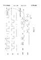
- FIG. 1is a block diagram representing a basic floating gate memory device for an integrated circuit which includes the logic for terminating a load cycle according to the present invention.
- FIG. 1is a simplified drawing of the basic components of a floating gate memory device formed on an integrated circuit. It is meant to represent the components of commercially available flash EPROM or EEPROM devices, which are supplemented with the novel pattern match logic, and protocol logic for determining the end of the program load cycle of the present invention.
- the deviceincludes a floating gate memory array 10. Coupled with the array are an X decoder 11, a Y decoder 12, and Y pass gates 13.
- Program and erase voltage sources 14are coupled with the array to supply a voltage on line 15 for word lines being programmed or erased, a voltage on line 16 for source terminals of cells in the array being programmed or erased, and a voltage on line 17 for bit lines coupled to cells being programmed or erased in the array.
- the mode control logic 18 and state machine 19are connected by line 40 to the program and line voltage sources 14, among other places.
- the mode control logic 18 and state machine 19 including an automatic program functionare included on an integrated circuit chip to control the read, erase, and program operations as known in the floating gate memory art.
- the state machinegenerates control signals generally represented by arrow 20 which manage the various operations of the device.
- the mode control logicis responsive to control signals received at control input logic 21 on the chip.
- the control inputsinclude, for example, a chip enable CE, an output enable OE, and a write enable WE signal on inputs represented by arrow 22.
- the control input logicsupplies control signals on line 23 to the mode logic 18.
- Addressesare received on input bus 24, and supplied to an address latch and buffer 25.
- the addresses at the output of the address latch and buffer 25are supplied on line 26 to the X decoder 11, the Y decoder 12, and to a command address/data latch 27.
- Input data and output dataare supplied on I/O pins represented by arrow 28 through data I/O circuitry 29.
- the incoming datais supplied on line 30 to the command address/data latch 27, and to a program data buffer 31.
- Output datais received on line 32 from sense amplifiers 33, which are coupled to the Y pass gates 13 across line 34 to receive
- the command address/data latch 27is coupled to a command address/data decoder 35, which decodes patterns in the incoming address and data stream which indicate certain functions to be performed.
- the output of the decoderis supplied on line 36 to the mode logic 18, which manages the various operations.
- one of the operationsis an autoprogram mode which involves automatically loading into the program data buffer and storing a block of data, with an automatic program verify operation.
- pattern match logic 37is coupled with the address latch and buffer 25, and the data I/O circuitry 29 to indicate during the program load cycle of the autoprogram operation when the incoming stream of addresses and data segments match a pre-specified pattern, such as consecutive matching addresses, consecutive matching address/data segment combinations, or an address which matches a pre-specified command address outside the address space used in programming the floating gate memory array 10.
- the output of the pattern match logicis supplied on line 38 to the mode logic 18 to signal the end of the program load cycle.
- the state machineinitiates the autoprogram process, storing the data from the program data buffer 31 across line 39 into the floating gate memory array 10, and automatically verifying the programming operation.
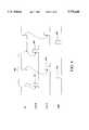
- FIG. 2illustrates the prior art protocol timing for determining the end of the program load cycle.
- the chip enable and write enable signalsare toggled from high to low as indicated at point 50.
- an input addresssuch as hex 5555 is latched in the command address/data latch 27.
- a second address in the command sequenceis loaded, such as hex 2AAA.
- the third address in the command sequenceis loaded at point 52, such as hex 5555.
- the autoprogram cycleis initiated by the mode control logic 18.
- a new addressis received, such as A0, A1 . . . , A127, for a case in which there are 128 addresses in a page of data to be stored in the program data buffer 31.
- the data segment for the previous addressis loaded, such as data segments D0, D1, . . . D127.
- a pulse of at least 100 microseconds, such as the pulse 53, in one of the control signalsis issued.
- the program process for the stored datais initiated as indicated by the arrow 54 by a transition in the output enable OE signal.
- this protocolsuffers the disadvantage that all segments of data in the page must be loaded for any program cycle, and the disadvantage that the 100 microsecond pulse is required to initiate the program process.
- FIG. 3shows the protocol timing according to the present invention.
- an address sequence corresponding to a commandis latched on the first three falling edges of the control signals, such as at edges 60, 61, and 62.
- a program load operationis executed in which the addresses A0, A1 through Ax are loaded on sequential falling edges of the control signal.
- the corresponding data segments D0 through D1, . . . Dxare loaded.
- the program processis begun as indicated by arrow 63.
- a 300 nanosecond pulse ending at edge 66is required in this embodiment for synchronization of the state machine before the autoprogram process starts.
- the patternincludes two sequential addresses in the address stream which match, such as Ax followed by Ax as shown in the region 64.
- matching sequential data for the corresponding addresses as shown in the sequence 65may be required to indicate the end of the program load segment of the autoprogram process.
- This processallows for explicit indication of the end of the program load segment of the autoprogram process upon an address or data transition in the sequence.
- the length of the block of data being loadedcan be arbitrary, from 1 byte to the full size of the page buffer.
- FIGS. 11A and 11Bshow an alternative pattern for detecting the end of the page load process.
- the locations into which data is to be storedare identified by addresses within an address field for the memory device.
- the addresseshave a page address segment and page buffer address segment.
- the page buffer (or bit latch) address segmentis identified by trace 70 while the page address is indicated by trace 71.
- the control signals including chip enable, write enable, and output enableare switched as shown in the figure.
- the same reference numerals used in FIG. 3are used in FIG. 11A where appropriate.
- the command sequenceis latched on the edges 60, 61, and 62 as before.
- the low order address field which stores the bit latch addresswill include a portion of the command code as indicated.
- the high order address fieldwill include the balance of the command code (not shown).
- the address command code to begin the load processis actually a 15 bit address (A0 to A14) rather than the 8 bit addresses indicated by the hex values 55, AA, and 55 of FIG. 11A.
- These two higher order fields of the command sequencecould be included in the page address field shown along trace 71, or included in a field that is intermediate between the bit latch address and the page address depending on a particular implementation.
- a dummy load addressis supplied to the page address field during the interval 72.
- the dummy load address 72is latched in the fourth cycle of the sequence, along with the first bit latch address A0.
- This load addressis held constant while the sequence of bytes and bit latch addresses are loaded to define the block to be stored.
- the data valuesare not shown. However, they will be timed just as shown in FIG. 3. In order to indicate the end of the load sequence, as shown in FIG.
- the page address field on trace 71is changed from the dummy load address 72 to the actual page address 73 within the address field for the memory.
- the command logicdetects this transition from the dummy load address to the page address, and starts the program process as indicated by arrow 74.
- a 300 nanosecond pulse ending by transition 66 in the chip enable signalis used to ensure that the state machine is synchronized to begin the programming process.
- the pattern of FIG. 11Ahas the advantage that it does not require an extra dummy cycle in which the address and/or data are repeated as shown in FIG. 3.
- FIG. 11Bshows another alternative pattern which uses the page address segment of the addresses being received to indicate the end of the load cycle.
- the actual page address for the data being loadedis latched as indicated in field 75.
- the actual page addressis latched in the fourth cycle of the sequence along with the bit latch address A0.
- the page addressis changed to a dummy start program address 76 which is outside the address field for the memory.
- the dummy start program addressis detected by the command logic, which then initiates the program process as indicated by arrow 77.
- the 300 nanosecond pulse of the chip enable signalmay be necessary again to ensure synchronization of the circuitry.
- FIGS. 4, 5, and 6pattern match logic and timing diagrams for the incoming address and data stream are described.
- the logic of FIGS. 4 and 5is applied here is applied to an address input buffer. Identical circuitry can be used with a data input buffer when data matching is required, and will not be not described again.
- an address input pad 400is included on the chip.
- the signal on the pad 400is supplied to an address buffer 401.
- the output of the address bufferis the address bit A(i) on line 402.
- the address pad 400is also connected through a pass gate 403 which is controlled by the signal CLKM.
- the output of the pass gate 403is supplied to a latch made up of inverters 404 and 405.
- the output of the latchis supplied through a pass gate 406 which is controlled by the signal CLKS.
- the output of pass gate 406is supplied to a latch composed of inverters 407 and 408.
- the data in the latch made up inverters 407 and 408is supplied through inverter 409 as a first input to an exclusive NOR gate 410.
- the data in the latch composed of inverters 404 and 405is supplied through inverter 411 as a second input to the exclusive NOR gate 410.
- the output of the exclusive NOR gate 410indicates an address match for the bit supplied on the pad 400, as indicated by the signal ADMTCH (i) on line 412.
- All of the address match signals ADMTCH 0 through N-1(where N is the number of address bits) are supplied to the circuitry shown in FIG. 5.
- the match signals for bits 0 and 1are supplied to NAND gate 415, and the match signals for bits 2 and 3 are supplied to NAND gate 416.
- the address match signals for bits 4 and 5are supplied to NAND gate 417.
- Address match signals for bits 6 and 7are supplied to NAND gate 418, and so on, until address match signals for bit N-2 and for bit N-1 are supplied to NAND gate 419.
- the output of the NAND gates 415 through 419are supplied to a multiple input NOR gate 420.
- the output of the NOR gateis supplied through NAND gate 421, which receives as a second input a compare clock signal CMP on line 422.
- the output of NAND gate 421is supplied through inverter 423 as a match signal on line 424, which is in turn supplied to the mode logic to indicate the detection of the sequential matching addresses.
- the timing of the control signals CLKM, CLKS, and CMPis illustrated in FIG. 6 with reference to the chip enable control signal CE.
- the CLKM signalincludes a pulse at the falling edge of the chip enable signal.
- the signal CLKSincludes a pulse at the rising edge of the chip enable signal.
- the control signal CMPis a pulse issued after the falling edge and before the rising edge of the chip enable signal, beginning after detection of the command sequence to start the autoprogram operation.
- the signal CMPis disabled during the first address and data loading cycle.
- a current address in the sequenceis latched through the pass gate 403 into the latch composed of inverters 404 and 405 in response to the CLKM signal pulse 451.
- the CMP pulse 452is issued which causes comparison of the address match signals, to occur between a previous address, and the current address which has just been latched.
- the current addressis shifted through the pass gate 406 in response to the CLKS pulse 453 into the latch composed of inverters 407 and 408.
- the CLKM pulse 454is issued. This causes the current address to be stored in the latch composed of inverters 404 and 405, while the previous address in the stream is stored in the latch composed of inverters 407 and 408.
- the current and the previous addressesare compared in response to the CMP signal pulse 455.
- FIGS. 4 and 5Although the logic of FIGS. 4 and 5 is shown for the address signals, the same logic is used for data signals, if the pattern to be detected includes matching segments of data in the stream.
- This logiccan be adapted as known in the art to detect a variety of patterns of data occurring in the address and data stream which suits the needs of the particular implementation.
- the latch composed of inverters 407 and 408might be replaced by a non-volatile store which holds a bit of a command address as discussed above, which falls outside the address space used in the program load operation, to be matched with the incoming data stream.
- FIG. 7illustrates an architecture of a segmentable flash EEPROM array according to the present invention, in which two columns of flash EEPROM cells share a single metal bit line.
- FIG. 7shows four pairs of columns of the array, where each pair of columns includes flash EEPROM cells in a drain-source-drain configuration.
- the first pair 120 of columnsincludes a first drain diffusion line 121, a source diffusion line 122, and a second drain diffusion line 123.
- Word lines WL0 through WL63each overlay the floating gates of a cell in a first one of the pairs of columns and a cell in the second one of the pairs of columns.
- a first pair 120 of columnsincludes one column including cell 124, cell 125, cell 126, and cell 127. Not shown are cells coupled to word lines WL2 through WL61.
- the second one of the pair 120 of columnsincludes cell 128, cell 129, cell 130, and cell 131.
- a second pair 135 of columnsis shown. It has a similar architecture to the pair 120 of columns except that it is laid out in a mirror image.
- the transistor in the first one of the pair of columnsincludes a drain in drain diffusion line 121, and a source in the source diffusion line 122.
- a floating gateoverlays the channel region between the first drain diffusion line 121 and the source diffusion line 122, and the word line WL1 overlays the floating gate of the cell 125 to establish a flash EEPROM cell.
- the column pair 120 and column pair 135share an array virtual ground diffusion 136 (ARVSS).
- ARVSSarray virtual ground diffusion 136
- the source diffusion line 122 of column pair 120is coupled to the ground diffusion 136.
- the source diffusion line 137 of column pair 135is coupled to the ground diffusion 136.
- each pair 120 of columns of cellsshares a single metal line.
- a block right select transistor 138 and a block left select transistor 139are included.
- the transistor 139includes a drain in the drain diffusion line 121, a source coupled to a metal contact 140, and a gate coupled to the control signal BLTR1 on line 141.
- the right select transistor 138includes a source in the drain diffusion line 123, a drain coupled to the metal contact 140, and a gate coupled to the control signal BLTR0 on line 142.
- the select circuitryincluding transistors 138 and 139, provides for selective connection of the first drain diffusion line 121 and a second drain diffusion line 123 to the metal line 143 (MTBL0) through metal contact 140.
- column pair 135includes left select transistor 144 and right select transistor 145 which are similarly connected to a metal contact 146.
- Contact 146is coupled to the same metal line 143 as is contact 140 which is coupled to column pair 120.
- the metal linecan be shared by more than two columns of cells with additional select circuitry.
- the architecture shown in FIG. 7is based upon a drain-source-drain unit forming two columns of cells which are isolated from adjacent drain-source-drain units to prevent leakage current from adjacent columns of cells.
- the architecturecan be extended to units of more than two columns, with appropriate tolerances for leakage current in the sensing circuitry, or other controls on current leakage from unselected cells.
- fourth and fifth diffusion linescould be added within a given isolated region to create a drain-source-drain-source-drain structure which provides four columns of cells.
- the arraymay be repeated horizontally and vertically as required to establish a large scale flash EEPROM memory array.
- column pairs 120 and 150 which share a word lineare repeated horizontally to provide a segment of the array. Segments are repeated vertically.
- a group of segmentse.g., eight segments having respective word lines coupled to a shared word line driver may be considered a sector of the array.
- word line WL63'may share a word line driver with word line WL63.
- eight word linesshare a single word line driver.
- the additional decoding provided by the left and right select transistors (139, 138 for segment 120)allows the shared word line configuration.
- the shared word line configurationhas the disadvantage that during a sector erase operation, eight rows of cells all receive the same word line voltage, causing a word line disturbance in cells that are not desired to be erased.
- this disturbance problemcan be eliminated by insuring that all sector erase operations decode for segments including all rows of cells coupled to the shared word line drivers. For eight word lines sharing a single driver, a minimum sector erase of eight segments may be desired.
- FIG. 8is a schematic block diagram of a flash EEPROM array including a page mode programming function meant to illustrate certain features of the present invention.
- the flash EEPROM memory module shown in FIG. 8includes a main flash EEPROM array, including sectors 170-1, 170-2, 170-3, 170-N, each sector including eight segments (e.g., SEG0-SEG7).
- a plurality of sets of shared word line drivers 171-1, 171-2, 171-3, 171-Nare used to drive the shared word lines of the eight segments in the respective sectors.
- shared word line drivers 171-1there are 64 shared drivers for sector 170-1. Each of the 64 drivers supplies an output on line 172. Each of these outputs is used to drive eight word lines in respective segments of the sector 170-1 as schematically illustrated in the figure by the division into eight sets of 64 lines.
- block select drivers 173-1, 173-2, 173-3, 173-Nare also coupled to the array.
- the block select driverseach drive a left and right block select signal for each segment.
- the segmentsare implemented as shown in FIG. 7, there is a BLTR1 and BLTR0 block select signal pair supplied for each set of 64 word lines.
- N global bit lines in the flash EEPROM arraythere are N global bit lines in the flash EEPROM array.
- the N global bit linesare used to allow access to the 2N columns of flash EEPROM cells in the array for the data in circuitry and sense amps 191.
- the column select decoder 175is coupled to the page program bit latches/verify block 190, including at least one bit latch for each of the N bit lines.
- the column select decoder 175is coupled to the data in circuitry and sense amps 191.
- Data bus line 192is 16 bits wide and provides input data to the data in circuitry and sense amps 191.
- Data bus line 192also provides 16 bits of output data. Together, these circuits provide data in and out circuitry for use with the flash EEPROM array.
- the N bit lines 174are coupled to a column select decoder 175.
- N1024 for a total of 1024 bit lines.
- the block select drivers 173-1 through 173-Nare coupled to a block decoder 176.
- the shared word line drivers 171-1 through 171-Nare coupled to row decoder 177.
- the column select decoder 175, block decoder 176, and row decoder 177receive address signals on the address in line 178.
- the page program bit latches/verify block 190includes a page buffer having N latches, one for each of the N bit lines. Thus, a page of data may be considered N bits wide, with each row of cells two pages, page 0 and page 1, wide. Pages in a given row are selected using the left and right decoding described above.
- the page program bit latches/verify block 190includes program verify circuitry for data stored in the N bit latches and the N bits wide page of data programmed to a selected row of cells in the array. An example of this circuitry is described below.
- Selectable voltage sources 179are used to supply the reference potentials for the read, program, and erase modes for the flash EEPROM array as conceptually illustrated in the figure, through the word line drivers 171-1 to 171-N and through the bit lines.
- the virtual ground lines in the arrayare coupled to the virtual ground driver 181 providing potentials for the various modes to the virtual ground terminals in the array. Also, p-well and n-well reference voltage sources 199 are coupled to the respective wells of the array.
- the 64 word line driverssuch as word line drivers 171-1, are used with 512 (64 ⁇ 8) rows in the array.
- the additional decoding provided by the block select driverse.g., 173-1) allows for the shared word line layout.
- the cells in the preferred embodimentare configured for a sector erase operation that causes charging of the floating gate (electrons entering the floating gate) such that upon sensing, an erased cell, is non-conducting.
- the architectureis configured for a page program which involves discharging a floating gate (electrons leaving the floating gate) such that upon sensing, a programmed cell is conducting.
- a mode control state machine 185which controls operation of the device for reading, programming, and erasing.
- the inputs to the mode control state machineinclude the pattern match signal on line 186.
- an input on line 189is supplied from the command address/data decoder as mentioned before. This provides for detecting the end of a program load cycle in an automatic program operation using the page program bit latches/verify circuitry, in response to the pattern match signal on line 186.
- a 100 microsecond chip enable pulsecan be indicated as pointed out by line 187. However, this may not be necessary for a particular implementation.
- the substrate or the p-well of the cellis grounded. This results in a Fowler-Nordheim tunneling mechanism for discharging the floating gate.
- the erase operationis executed by applying negative 8 volts to the source, and positive 12 volts to the gate, with the drain left floating.
- the p-wellis biased at negative 8 volts. This results in a Fowler-Nordheim tunneling mechanism to charge the floating gate.
- the read potentialsare 1.2 volts on the drain, 5 volts on the gate, and 0 volts on the source. This sets up the ability to do a sector erase using word line decoding to select cells to be erased.
- the erase disturbance condition for unselected cells within a segmentresults in -8 volts on the drain, 0 volts on the gate, and -8 volts on the source. This is well within the tolerances of the cells to withstand these potentials without causing significant disturbance of the charge in the cell.
- the program disturbance conditionsfor cells which share the same bit line in the same segment are 6 volts on the drain, 0 volts on the gate (or optionally 1 volt), and 0 volts or floating on the source. There is no gate to drain drive in this condition and it does not disturb the cell significantly.
- hot electron injectionmay be used for charging up the floating gate by applying high positive voltages to the gate and drain, and a low voltage to the source.
- the page program bit latch/verify block 190 of FIG. 8includes program verify circuitry which resets on a bit by bit basis, the data in the page buffer that passes verify.
- the drain of transistor 502 and the drain of transistor 504are coupled to the metal line 143 (MTBL0).
- the drain of transistor 506 and the drain of transistor 508are coupled to the metal line 152 (MTBL1).
- the source of transistor of 504 and the source of transistor of 506are coupled to the array virtual ground 136 (ARVSS).
- Signal DMWLX on line 570is coupled to gate of transistor 504 and gate of transistor 506.
- the array virtual ground line 136 (ARVSS)is coupled to the metal line 143 (MTBL0) and the metal line 152 (MTBL1) via transistor 504 and transistor 506, respectively.
- Data I/O line 574is coupled to the source of transistor 502.
- Data I/O line 576is coupled to the source of transistor 508.
- Signal BLISOB on line 572is coupled to the gate transistor 502 and the gate of transistor 508. When signal BLISOB is high, metal line 143 is coupled to data I/O line 574 via transistor 502, and metal line 152 is coupled to data I/O line 576 via transistor 508.
- Data I/O line 574is coupled to the drain of transistor 542.
- the source of transistor 542is coupled to ground, and the gate of transistor 542 is coupled to signal DMWL on line 588.
- the data I/O line 574is pulled down when the signal DMWL is high.
- Data I/O line 574is further coupled to the drain of column select transistor 544.
- the source of transistor 544is coupled to node 551.
- the gate of transistor 544is coupled to signal Y0 on line 590.
- a data-in buffer 550is coupled to the source of pass gate 552.
- the drain of pass gate 552is coupled to node 551.
- Pass gate 552is controlled by signal DINL on line 592.
- Sense amp 554is also coupled to node 551. Sense amp 554 is controlled by signal SAEB on line 594. The output of sense amp 554 is coupled to the drain of pass gate 556. The source of pass gate 556 is coupled to latch circuit 557. Pass gate 556 is controlled by signal SARD on line 596.
- the latch circuitincludes inverters 558 and 560.
- the input of inverter 558is coupled to the source of pass gate 556.
- the output of inverter 558is coupled to the input of inverter of 560, and the output of inverter 560 is coupled to the source of pass gate 556.
- the output of latch circuit 557is also coupled to a first input to NOR gate 562.
- a second input to NOR gate 562is coupled to signal RESLATB on line 598.
- the output of NOR gate 562is coupled to the gate of transistor 564.
- the drain of transistor 564is coupled to node 551, and the source is coupled to ground.
- Data I/O line 576which is coupled through transistor 508 to bit line 152 is connected in a similar maimer.
- line 576is coupled to the drain of transistor 548.
- the source of transistor 548is coupled to ground, and the gate is coupled to signal DMWL on line 588.
- the drain of transistor 546is also coupled to data I/O line 576.
- Signal Y0is coupled to the gate of transistor of 546.
- the source of transistor 546is coupled to node 591 which corresponds to node 551 for the other side.
- a corresponding set of DIN buffer 550, sense amp 554, latch circuit 557 and associated circuits coupled to node DATA1 591are not shown.
- circuits similar to DIN buffer 550, pass gate 552, sense amp 554, pass gate 556, latch circuit 557, NOR gate 562, and transistor 564are similarly configured and coupled to node DATA1 591.
- Each data I/O line 574, 576has a bit latch/verify logic circuit coupled to it, comprised generally of the NAND gate 524 and inverter 526 for data I/O line 574, and of NAND gate 534 and inverter 536 for data line I/O 576.
- the drain of pass gate 522is coupled to data I/O line 574
- the source of pass gate 522is coupled to a first input of NAND gate 524.
- a second input to NAND gate 524is coupled to signal BLATEN on line 582.
- the output of NAND gate 524is coupled to the input of inverter 526.
- the input power for NAND gate 524 and inverter 526is coupled to signal LATCHPWR on line 580.
- Signal LATCHB on line 578is coupled to the gate of pass gate 522.
- the output of inverter 526is coupled to the first input of NAND gate 524, the gate of transistor 510, and the gate of transistor 530.
- the drain of transistor 510is coupled to signal ABLRES1 on line 577.
- the source of transistor 510is coupled to ground.
- the drain of transistor 530is coupled to signal DLPWR on line 586.
- the source of transistor 530is coupled to the drain of transistor 528.
- the gate of transistor 528is coupled to signal DLCTL on line 584, and the source of transistor 528 is coupled to data I/O line 574.
- the logic high levelenables transistor 510 which causes a logic low level on line 577.
- line 577is coupled to ground which causes signal ABLRES1 to a logic low level.
- Transistors 514 and 516comprise an inverter, which, together with transistors 510 and 512, provides a NOR logic function.
- Transistor 514is a p-channel transistor with the source coupled to Vcc and the drain coupled to the drain of n-channel transistor 516.
- Line 577is coupled to the drains of transistors 514 and 516.
- n-channel transistor 516The source of n-channel transistor 516 is coupled to ground, and the gates of transistors 514 and 516 are coupled to signal PGPVB on line 599.
- Inverters 51 8 and 520are coupled in series.
- Line 577provides the input to inverter 518.
- the output of inverter 518provides the input of inverter 520, and the output of inverter 520 provides signal ABLRES on line 579.
- signal ABLRESis a logic low level.
- Transistor 514provides a pull-up to line 577 which can be driven to a logic low level by enabling either transistor 510 or transistor 512.
- transistor 516is that during default state PGPVB on line 599 is "HIGH", and all the gates of transistors 510, 512 . . . are low, so that if there is no transistor 516, ABLRES1 on line 577 is floating. Transistor 516 is added to help line 577 to pull low in this case.
- PGPVB on line 599is active "LOW"
- transistor 516is off and transistor 514 provides a pull-up to line 577.
- a mirrored arrangement of circuits also controlled by signals LATCHB, LATCHPWR, BLATEN and DLCTLare coupled to data I/O line 576.
- the drain of pass gate of 532is coupled to data I/O line 576.
- the gate of pass gate 532is coupled to signal LATCHB on line 578.
- the source of pass gate 532is coupled to a first input to NAND gate 534.
- a second input to NAND gate 534is coupled to signal BLATEN on line 582.
- the output of NAND gate 534is coupled to the input of inverter 536.
- Signal LATCHPWR on line 580provides input power to NAND gate 534 and inverter 536.
- the output of inverter of 536is coupled to the first input of NAND gate 534, the gate of transistor of 512, and the gate of transistor 538.
- Signal DLPWR on line 586is coupled to the drain of transistor 538.
- the source of transistor 538is coupled to the drain of transistor 540.
- the gate of transistor of 540is coupled to signal DLCTL on line 584, and the source of transistor 540 is coupled to data I/O line 576.
- the source of transistor 512is coupled to ground and the drain of transistor 512 is coupled to line 577.
- the page program and automatic verify circuit of the flash EEPROM array as shown in FIG. 9executes the page program and program verify in a series of stages.
- the stagescan be generalized as a (1) data loading stage; (2) data program stage; (3) read the array data stage; (4) reset bit latch stage; and (5) retry stage.
- the operation of the page program and automatic verify of the flash EEPROM arrayis described with reference to data I/O line 574.
- Page program and automatic verifyare similarly performed using data I/O line 576 that is coupled to another memory cell.
- the page program and automatic verify circuitincludes similar circuitry for all data I/O lines needed to program a page of memory cells in the flash EEPROM array.
- signal LATCHPWR on line 580, signal LATCHB on line 578, and signal BLATEN on line 582are supplied with 5 volts to activate data latch circuitry 524 and 526 for operation.
- Signal LATCHPWR on line 580supplies voltage to NAND gate 524 and inverter 526 for operation.
- Signal BLATEN on line 582enables latch circuitry 524 and 526 to receive inputs.
- Signal LATCHB on line 578enables pass gate 522 to couple data I/O line 574 with the first input of NAND gate 524.
- Signal BLISOB on line 572is at a logic low level which disables transistor 502. Disabling transistor 502 isolates data I/O line 574 from the metal line 143 (MTBL0).
- Signal DLCTL on line 584is at a logic low level which disables pass gate 528.
- Signal DLPWRis at a logic high level having a voltage of Vcc that is approximately 5 volts.
- Signal DMWI, on line 588is at a logic low which prevents transistor 542 from coupling data I/O line 574 to ground.
- Signal Y0 on line 590is a logic high level which enables transistor 544 to conduct.
- Signal Y0is a decoded signal which enables data I/O line 574 to access a corresponding one of 16 DIN buffers (e.g. buffer 550) during the data loading stage.
- Signal DINL on line 592is a logic high which enable pass gate 552. Input data from DIN buffers 550 is transferred via pass gate 552 to data I/O line 574.
- the data from DIN buffer 550is transferred to the first input of NAND gate 524. If data from DIN buffer 550 is a logic high level, the logic high level received at the first input of NAND gate 524 causes a logic low output. The logic low output of NAND gate 524 provides the input to inverter 526 which provides a logic high output. NAND gate 524 and inverter 526 comprise the bit latch circuitry which latches the data received at the first input of NAND gate 524. The logic high level at the output of inverter 526 enables pass gate 530 and transfers signal DLPWR on line 586 to pass gate 528. However, during the data loading stage, signal DLCTL on line 584 is a logic low which disables pass gate 528 from conducting signal DLPWR to data I/O line 574.
- the logic low level received at the first input of NAND gate 524causes a logic high output.
- the logic high output of NAND gate 524provides the input to inverter 526 which provides a logic low output that is stored in latch circuitry 524 and 526.
- the logic low at the output of inverter 526disables pass gate 530 and the transfer of signal DLPWR on line 586 via pass gate 528 to data I/O line 574.
- the bit latch circuit of NAND gate 524 and inverter 526stores either the logic high level or the logic low level of the input data which corresponds to the data transferred from DIN buffer 550.
- bit latches for up to the entire page of 1024 bitsare loaded in 16 bit segments relying on the protocol outlined above to detect the last 16 bit segment in the block. Bit latches not loaded are set to zero.
- signal LATCHB on line 578is disabled.
- Signal LATCHB on line 578is set to a logic low to disable inputs to latch circuitry 524 and 526.
- Signal LATCHPWRis set to a high voltage to provide power to latch circuitry 524 and 526.
- Signal BLATEN on line 582is set to a high voltage level to enable the output of latch circuitry 524 and 526.
- Signal BLISOB on line 572is set to a high voltage level to enable transistor 502.
- Transistor 502couples data I/O line 574 to metal line 143.
- Signal DLCTL on line 584is set to a high voltage level to enable pass gate 528.
- Signal DLPWR on line 586is set to a high voltage.
- Signal Y0 on line 590is a logic low level to disable transistor 544.
- Signal DINLis a logic low level which decouples input data from DIN buffer 550 from data I/O line 574.
- Signal SAEBis a logic low level to disable sense amp 554.
- signal DLPWR on line 586is transferred to data I/O line 574.
- Signal DLPWRprovides programming power to program a memory cell in the flash EEPROM array.
- pass gate 530is enabled to permit signal DLPWR to pass through pass gate 528.
- Signal BLISOB on line 572enables transistor 502 and couples signal DLPWR to the metal line 143 (MTBL0).
- enabling signal BLTR1 on line 141 or BLTR0 on line 142couples a column of cells to the metal line 143 and provides the programming voltage from signal DLPWR to program a particular memory cell 125 or 129 on the word line which is changed to -8 volts. For instance, if BLTR1 on line 141 is selected and word line WLI is selected, the programming voltage from signal DLPWR is directed to memory cell 125.
- the circuitryAfter the data from latch circuitry 524 and 526 is programmed to the memory cell, the circuitry is ready to verify automatically that the data was properly programmed in the data write stage. This involves a five step sequence (A through E) for deciding whether to reset the bit latch as follows:
- READthe real data from the non-volatile bit through the associated sense amp (all 16 sense amps are activated at the same time, i.e. 16 bits are read at the same time).
- the sensing resultis stored in latch 557 of FIG. 9.
- BLISOB(572) must be high (ON), selected Y (544, 546 and 14 more of such devices) is on, sense amp (SA) 554 is activated (and 15 other SA), SARD (596) is high to allow the sensing result pass to the latch (557) and LATCHB (578), DLCTL (584) are at low voltage (OFF) so that during this READ step, the bit latch consisting of 524 and 526 will not be disturbed.
- the selected cell threshold voltageis sensed by the SA (554) via data line 574 and then stored in latch 557, after a certain amount of time which is long enough for the SA (554) to do the sensing. If after programming, the cell's threshold voltage (VT) is low enough (to the point that the SA 554 can tell that the cell is at low VT state) then the output of the inverter (560, or input of 558) will reflect a low level, SARD (596) is off and then SA (544) is disabled. The low level is stored in latch (557), no matter what read happens during the next 4 steps in sequence until the new locations need to be read again. If after programming, the selected cell VT is still read high, then the output of inverter 560 is at high level, i.e. a logic high level is latched in latch 557. Note that RESLATB (598) is HIGH in this step so that whether latch 557 latched high or low will not affect device (564) because device 564 is OFF anyway.
- DISCHARGE DATA LINES(all including selected and deselected) The purpose of this step will be explained in STEP D).
- the way of discharging the data line 574is by activating DMWL (588) to high turning on transistors 542 and 548, LATCHB at low, DLCTL at low, with all sense amps disabled, 564 and 552 are off.
- Transistor 542discharges charge stored in data line 574.
- BLISOB (572)is at low level to isolate the long metal-bit-line (MTBL0) from the data line (574) so that the discharge sequence can be achieved faster.
- step DDMWL is at low level, BLISOB is still at low level, whether the selected 16 data lines of the same word and other de-selected data lines should be precharged to a high voltage level or not is decided by the data which is stored in the bit latch. For example, in FIG.
- DLCTL(584) is switched from low to high, and data line 574 is precharged to a high level by connecting DLPWR (a V cc level power source for this instance) to the data line (574) via devices 530 and 528 if the output of inverter 526 (which is the gate of 530) is latched at HIGH level. Otherwise DLPWR cannot precharge data line 574 to a high level and the data line 574 should be still at a low voltage level due to step B.
- DLPWRa V cc level power source for this instance
- LATCHB(578) is switched from low level to a high level, and RESLATB (598) switches from high to low in order to reset the bit latch (which consists of NAND gate 524 and inverter 526) by turning on transistor 564, if the output of inverter 560 is (latched) low (from step A). Since the selected cell is at low VT already, the bit latch content shall be reset so that for the next programming, high voltage pulse sequence, the cell which is at low VT shall not be programmed to low VT again. There is a chance that the bit latch had been reset from a previous verify loop step D) or was at reset state even before the first programming sequence.
- the subsequent reset bit latch stepis of no effect to the bit latch for the former case; and for the latter case whether the selected cell is at high VT or not will not affect the bit latch because if the cell is at high VT, there is no resetting the bit latch (transistor 564 is OFF, from Steps A and D) and bit latch was at reset state. If the cell was at low VT, then resetting the bit latch again makes no difference to the contents of the bit latch. There is no comparison circuit needed in this implementation.
- LATCHBis a global signal to all the bit latches in the FLASH EEPROM design and the high level at the gates of 522, 532 . . . results in all bit latches being coupled to the associated data lines which means that the node of the output of inverter 526 will encounter a charge sharing with the associated data line (574, for example).
- the driving capability of inverter 526is designed to be a weak device in order that a proper data can be set (to fight against inverter 526) into the bit latch. So when LATCHB (578) is HIGH, weak inverter (526) suffers a charge sharing issue which results in the uncertainty of the integrity of the bit latch.
- steps B) and C)are to put the proper voltage level at the data lines before getting into step D), i.e. before LATCHB (578) switches from low to high to avoid any "charge sharing issues", even though the circuitry can be designed as mentioned above to ensure proper operation without them.
- step B)all data lines are discharged to low level and then at step C) only those data lines whose associated bit latches "stored" high level will be precharged to a high level.
- steps B) and C)are optional steps inserted here for safety in the design.
- the page program and automatic verify circuit of FIG. 9provides the unique feature of automatically verifying a memory cell that is programmed.
- Latch circuitry 524 and 526stores the input data received from DIN buffer 550.
- the stored data in latch circuitry 524 and 526controls ABLRES1 which is set to a logic low level if there is at least one cell which needs to be programmed.
- Signal ABLRES Iremains a logic low level until all the page memory cells are verified during the program verify sequence which resets all latches (524 and 526) to a logic low level and resets signal ABLRES1 to a logic high level indicating a properly programmed memory cell.
- the program verify sequenceis automatic.
- Signal PGPVB on line 599is a logic low level to supply a charge to line 577 during automatic verify sequence.
- latch circuitry 526 and 524When latch circuitry 526 and 524 is reset, transistor 510 is disabled and the charge on line 577 is no longer discharged to ground.
- Signal ABLRES1 on line 577becomes a logic high level.
- the logic high levelprovides an input to inverter 518 which produces an output that provides an input to inverter 520 which provides the logic high level output of signal ABLRES on line 579.
- the logic high level of signal ABLRES on line 579provides a page programmed verify signal signifying the page of memory cells has passed program verify.
- Each memory cell within a page of memory cells in the arrayis able to activate a transistor 510 to cause signal ABLRES1 on line 577 to be a logic low level.
- any memory cell that does not pass program verify within a page of memory cells in the arraycan cause the output ABLRES to be a logic low level.
- the logic low level of ABLRES on line 579signals that at least one memory cell within the page of memory cells in the array is not properly programmed and verified.
- any memory cell not properly verifiedcan cause signal ABLRES on line 579 to be a logic low level.
- signal ABLRES on line 579is a logic high level.
- unsuccessfully programmed memory cellsare reprogrammed and reverified until signal ABLRES becomes a logic high level.
- the number of retriesare limited to prevent looping of the programming sequence if a page repeatedly fails program verification.
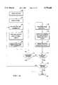
- FIG. 10provides a flow chart illustrating the program flow for the flash EEPROM circuit of FIG. 9.
- the processbegins by erasing the sector (e.g., sector 170-1) into which data is to be programmed (block 700). After erasing the sector, an erase verify operation is executed (block 701). Next, the page number, either 0 or 1, and the segment number, 1-8, is set by the host processor in response to the input address (block 702).
- the page bufferis loaded with a block including from one byte up to a full page (block 703).
- the page buffermay be loaded with an entire page of data, or a single byte of data, as suits a particular program operation. The end of the load portion of the autoprogram cycle is indicated by the pattern match described above.
- a verify operationis executed, in case the user does not pre-erase, or tries to reprogram the same data, to determine which cells need programming (block 704).
- the program potentialsare applied to the segment being programmed (block 705).
- a verify operationis executed in which the page is verified. In the verify operation, the programmed page is read and each corresponding read bit of data is stored in a sense amp data latch (block 715).
- the page bits which pass verifyare reset (block 722).
- the algorithmdetermines whether all page bits are turned off in the page buffer, ie., did all pages bits pass (block 723). If they are not all off, then the algorithm determines whether a maximum number of retries has been made (block 710), and if not, loops to block 705 to program the page again, such that the failed bits are reprogrammed. The bits which pass are not reprogrammed because the corresponding bits in the page buffer were reset to 0 during the verify operation. If the maximum number of retries has been made at block 710, then the algorithm is done (block 730), signaling an unsuccessful operation.
- the algorithmdetermines whether the sector has been finished, that is, whether both pages of the sector are to be written and both are completed (block 725). This is a CPU determined parameter. If the sector is not finished, then the algorithm loops to block 702 and updates the appropriate one of the page number or segment number. If the sector has been finished at block 725, then the algorithm is done (block 730).
- a new flash EEPROM array architecture with an autoprogram functionwhich detects the end of a load cycle in response to transitions in the address and/or data signals applied to the memory, has been provided.
- the architectureprovides for a very dense core array obtained by unique cell layouts, where two adjacent local drain bit lines share one common source bit line. Also, the layout has been optimized to allow use of a single metal line for every two columns of cells in the array. Further, the layout is further reduced by shared word lines, so that the word line driver pitch does not impact the size of the main array. Sector erase is feasible using segmentable architecture of the present invention. Also, the page program and automatic verify circuitry provides efficient and accurate programming of the memory cells. Thus, a high performance, reliable flash memory array can be achieved using these technologies.
- n-channel embodiment of the flash EEPROM arrayhas been disclosed. Those skilled in the art will recognize that p-channel equivalent circuits can be implemented using techniques known in the art. Furthermore, the architecture has been designed with respect to flash EEPROM cells. Many aspects of the architecture may be adapted to a variety of memory circuit arrays.
- the present inventionprovides a page programmed flash EEPROM device, in which the length of a block of data being stored in a given page program operation can be arbitrarily defined, and which does not require the 100 microsecond pulse to indicate the end of the program load segment of an automatic programming cycle.
- the systemis particularly suitable for high density integrated circuit memories, storing 16 megabits or more of data in a floating gate memory integrated circuit.
Landscapes
- Physics & Mathematics (AREA)
- General Physics & Mathematics (AREA)
- Engineering & Computer Science (AREA)
- Microelectronics & Electronic Packaging (AREA)
- Read Only Memory (AREA)
Abstract
Description
Claims (40)
Priority Applications (1)
| Application Number | Priority Date | Filing Date | Title |
|---|---|---|---|
| US08/596,380US5778440A (en) | 1994-10-26 | 1995-05-26 | Floating gate memory device and method for terminating a program load cycle upon detecting a predetermined address/data pattern |
Applications Claiming Priority (3)
| Application Number | Priority Date | Filing Date | Title |
|---|---|---|---|
| US08/325,467US5526307A (en) | 1992-01-22 | 1994-09-13 | Flash EPROM integrated circuit architecture |
| PCT/US1995/006762WO1996037826A1 (en) | 1995-05-26 | 1995-05-26 | Floating gate memory device with protocol to terminate program load cycle |
| US08/596,380US5778440A (en) | 1994-10-26 | 1995-05-26 | Floating gate memory device and method for terminating a program load cycle upon detecting a predetermined address/data pattern |
Related Parent Applications (1)
| Application Number | Title | Priority Date | Filing Date |
|---|---|---|---|
| US08/325,467Continuation-In-PartUS5526307A (en) | 1992-01-22 | 1994-09-13 | Flash EPROM integrated circuit architecture |
Publications (1)
| Publication Number | Publication Date |
|---|---|
| US5778440Atrue US5778440A (en) | 1998-07-07 |
Family
ID=46251796
Family Applications (1)
| Application Number | Title | Priority Date | Filing Date |
|---|---|---|---|
| US08/596,380Expired - LifetimeUS5778440A (en) | 1994-10-26 | 1995-05-26 | Floating gate memory device and method for terminating a program load cycle upon detecting a predetermined address/data pattern |
Country Status (1)
| Country | Link |
|---|---|
| US (1) | US5778440A (en) |
Cited By (88)
| Publication number | Priority date | Publication date | Assignee | Title |
|---|---|---|---|---|
| EP0801795A4 (en)* | 1995-01-05 | 1999-05-19 | Macronix Int Co Ltd | Advanced program verify for page mode flash memory |
| US6091666A (en)* | 1996-10-04 | 2000-07-18 | Sony Corporation | Nonvolatile flash memory with fast data programming operation |
| US6122203A (en)* | 1998-06-29 | 2000-09-19 | Cypress Semiconductor Corp. | Method, architecture and circuit for writing to and reading from a memory during a single cycle |
| US6389500B1 (en)* | 1999-05-28 | 2002-05-14 | Agere Systems Guardian Corporation | Flash memory |
| US20030026281A1 (en)* | 2001-07-20 | 2003-02-06 | Limaye Pradeep Shrikrishna | Interlocking SONET/SDH network architecture |
| US20030131186A1 (en)* | 2001-12-29 | 2003-07-10 | Wolfgang Buhr | Method and arrangement for programming and verifying EEPROM pages and a corresponding computer software product and a corresponding computer-readable storage medium |
| US20030177486A1 (en)* | 2002-03-13 | 2003-09-18 | Telefonaktiebolaget Lm Ericsson (Publ) | Method and system for performing SW upgrade in a real-time system |
| US20030182414A1 (en)* | 2003-05-13 | 2003-09-25 | O'neill Patrick J. | System and method for updating and distributing information |
| US20040040020A1 (en)* | 2002-08-22 | 2004-02-26 | Xuguang Yang | Electronic device with an update agent that employs preprocessing techniques for update |
| US20040068721A1 (en)* | 2000-11-17 | 2004-04-08 | O'neill Patrick | Network for updating firmware and / or software in wireless communication devices |
| US20040083472A1 (en)* | 2002-10-21 | 2004-04-29 | Rao Bindu Rama | System with required enhancements to syncML DM environment to support firmware updates |
| US20040103412A1 (en)* | 2002-11-21 | 2004-05-27 | Rao Bindu Rama | Software self-repair toolkit for electronic devices |
| US20040123282A1 (en)* | 2000-11-17 | 2004-06-24 | Rao Bindu Rama | Mobile handset with a fault tolerant update agent |
| US20040148597A1 (en)* | 2002-10-11 | 2004-07-29 | Lilley Patrick C. | System for optimizing distribution of information employing a universal dictionary |
| US20040166839A1 (en)* | 2002-04-19 | 2004-08-26 | Harri Okkonen | Communications network capable of determining SIM card changes in electronic devices |
| US20040168165A1 (en)* | 2002-11-13 | 2004-08-26 | Antti Kokkinen | Update system employing reference software to reduce number of update packages |
| US20040194081A1 (en)* | 2002-03-23 | 2004-09-30 | Iyad Qumei | Update system for facilitating firmware/software update in a mobile handset |
| US20040215755A1 (en)* | 2000-11-17 | 2004-10-28 | O'neill Patrick J. | System and method for updating and distributing information |
| US20040215702A1 (en)* | 2002-12-31 | 2004-10-28 | Glenn Hamasaki | Management of service components installed in an electronic device in a mobile services network |
| US20040226008A1 (en)* | 2002-11-22 | 2004-11-11 | Sid Jacobi | Update system for facilitating software update and data conversion in an electronic device |
| US20040230965A1 (en)* | 2003-02-28 | 2004-11-18 | Harri Okkonen | Mobile handset network that facilitates interaction between a generic intelligent responsive agent and a service broker server |
| US20040243993A1 (en)* | 2003-03-24 | 2004-12-02 | Harri Okonnen | Electronic device supporting multiple update agents |
| US20040243992A1 (en)* | 2003-01-21 | 2004-12-02 | Gustafson James P. | Update system capable of updating software across multiple FLASH chips |
| US20040250245A1 (en)* | 2003-06-04 | 2004-12-09 | Rao Bindu Rama | Network having customizable generators and electronic device having customizable updating software |
| US6851013B1 (en)* | 1999-12-15 | 2005-02-01 | Intel Corporation | Fast program mode |
| US20050039088A1 (en)* | 2003-08-12 | 2005-02-17 | Broadcom Corporation | High speed comparator for 10G SERDES |
| US20050039178A1 (en)* | 2003-06-27 | 2005-02-17 | Sunil Marolia | System and method for downloading update packages into a mobile handset in a carrier network |
| US20050055684A1 (en)* | 2003-07-29 | 2005-03-10 | Rao Bindu Rama | Mobile handset with update agent implemented in hardware |
| US20050071385A1 (en)* | 2003-09-26 | 2005-03-31 | Rao Bindu Rama | Update package catalog for update package transfer between generator and content server in a network |
| US20050102660A1 (en)* | 2002-04-12 | 2005-05-12 | Shao-Chun Chen | Initialization and update of software and/or firmware in electronic devices |
| US20050114504A1 (en)* | 2003-07-09 | 2005-05-26 | Sunil Marolia | Carrier network capable of conducting remote diagnostics in a mobile handset |
| US20050114852A1 (en)* | 2000-11-17 | 2005-05-26 | Shao-Chun Chen | Tri-phase boot process in electronic devices |
| US20050125412A1 (en)* | 2003-12-09 | 2005-06-09 | Nec Laboratories America, Inc. | Web crawling |
| US20050132351A1 (en)* | 2003-12-12 | 2005-06-16 | Randall Roderick K. | Updating electronic device software employing rollback |
| US20050141273A1 (en)* | 2003-12-31 | 2005-06-30 | Min-Gun Park | Flash memory system capable of inputting/outputting sector data at random |
| US20050153741A1 (en)* | 2003-10-03 | 2005-07-14 | Shao-Chun Chen | Network and method for registration of mobile devices and management of the mobile devices |
| US6925016B2 (en) | 2001-02-01 | 2005-08-02 | Nec Electronics Corporation | Semiconductor memory and method for entering its operation mode |
| US20050182697A1 (en)* | 2004-02-12 | 2005-08-18 | Rao Bindu R. | Device management network that facilitates selective billing |
| US20050216718A1 (en)* | 2003-02-11 | 2005-09-29 | Rao Bindu R | Electronic device supporting multiple update agents |
| US20050246331A1 (en)* | 2003-03-27 | 2005-11-03 | Microsoft Corporation | System and method for filtering and organizing items based on common elements |
| US20060143058A1 (en)* | 2000-11-17 | 2006-06-29 | Jeffrey Brunet | Operator network that routes customer care calls based on subscriber/device profile and CSR skill set |
| US20060175271A1 (en)* | 2005-01-31 | 2006-08-10 | Emrey David A | Apparatus and method of holding a golf score card and writing instrument, and golf bag and system incorporating the same |
| US20060258344A1 (en)* | 2002-08-22 | 2006-11-16 | Shao-Chun Chen | Mobile handset update package generator that employs nodes technique |
| US20070079306A1 (en)* | 2004-04-06 | 2007-04-05 | Iyad Qumei | Object ordering tool for facilitating generation of firmware update friendly binary image |
| US20070136628A1 (en)* | 2005-12-09 | 2007-06-14 | Advantest Corporation | Testing apparatus and testing method |
| US7343443B1 (en) | 2003-07-08 | 2008-03-11 | Hewlett-Packard Development Company, L.P. | Updated package generation based on analysis of bank dependency |
| US20080079539A1 (en)* | 2006-08-15 | 2008-04-03 | Daley Robert C | Friends Finder Service for a Mobile Device in a Network |
| US7356727B1 (en) | 2003-03-10 | 2008-04-08 | Hewlett-Packard Development Company, L.P. | Electronic device employing efficient fault tolerance |
| US7366125B1 (en) | 2003-07-24 | 2008-04-29 | Bbn Technologies Corp. | Extensible satellite communication system |
| US7434216B1 (en) | 2002-11-25 | 2008-10-07 | Hewlett-Packard Development Company, L.P. | Update package generator that employs genetic evolution to determine bank order |
| US7472380B1 (en) | 2002-09-23 | 2008-12-30 | Hewlett-Packard Development Company, L.P. | Processing system with component architecture platform support |
| US7480907B1 (en) | 2003-01-09 | 2009-01-20 | Hewlett-Packard Development Company, L.P. | Mobile services network for update of firmware/software in mobile handsets |
| US7543118B1 (en) | 2004-05-07 | 2009-06-02 | Hewlett-Packard Development Company, L.P. | Multiple variance platform for the management of mobile devices |
| US7548986B1 (en) | 2003-03-17 | 2009-06-16 | Hewlett-Packard Development Company, L.P. | Electronic device network providing streaming updates |
| US20090210401A1 (en)* | 2008-02-14 | 2009-08-20 | Kaufman Jr Gerald J | System And Method For Efficient Remote Data Access For Server Management |
| US7584466B1 (en) | 2003-06-16 | 2009-09-01 | Hewlett-Packard Development Company, L.P. | Management tree management in a mobile handset |
| US7657886B1 (en) | 2004-06-03 | 2010-02-02 | Hewlett-Packard Development Company, L.P. | Mobile device with a MMU for faster firmware updates in a wireless network |
| US7668612B1 (en) | 2003-09-18 | 2010-02-23 | Hewlett-Packard Development Company, L.P. | System and method for efficient manufacture and update of electronic devices |
| US7669195B1 (en) | 2003-07-31 | 2010-02-23 | Hewlett-Packard Development Company, L.P. | Electronic device network supporting compression and decompression in electronic devices and update generator |
| US7669197B1 (en) | 2002-09-12 | 2010-02-23 | Hewlett-Packard Development Company, L.P. | Embedded system employing component architecture platform |
| US7689981B1 (en) | 2003-02-28 | 2010-03-30 | Hewlett-Packard Development Company, L.P. | Mobile handset with efficient interruption point detection during a multiple-pass update process |
| US7689982B1 (en) | 2004-05-07 | 2010-03-30 | Hewlett-Packard Development Company, L.P. | Transparent linker profiler tool with profile database |
| US20100095293A1 (en)* | 2000-11-17 | 2010-04-15 | O'neill Patrick | Network for updating firmware and / or software in wireless communication devices |
| US7716276B1 (en) | 2003-11-17 | 2010-05-11 | Hewlett-Packard Development Company, L.P. | Network that supports user-initiated device management |
| US7725889B2 (en) | 2003-01-13 | 2010-05-25 | Hewlett-Packard Development Company, L.P. | Mobile handset capable of updating its update agent |
| US7747994B1 (en) | 2003-06-04 | 2010-06-29 | Hewlett-Packard Development Company, L.P. | Generator based on multiple instruction streams and minimum size instruction set for generating updates to mobile handset |
| US7747997B1 (en) | 2002-11-13 | 2010-06-29 | Hewlett-Packard Development Company, L.P. | Firmware update in electronic devices employing SIM card for saving metadata information |
| WO2010075746A1 (en)* | 2008-12-31 | 2010-07-08 | 深圳市同洲电子股份有限公司 | Nand flash state detecting device, system, electrical device and method |
| US7797693B1 (en) | 2003-12-12 | 2010-09-14 | Hewlett-Packard Development Company, L.P. | NAND mobile devices capable of updating firmware or software in a manner analogous to NOR mobile devices |
| US7881745B1 (en) | 2003-03-10 | 2011-02-01 | Hewlett-Packard Development Company, L.P. | Electronic device network employing provisioning techniques to update firmware and/or software in electronic devices |
| US7890427B1 (en) | 2003-01-09 | 2011-02-15 | Hewlett-Packard Development Company, L.P. | Authentication of notifications received in an electronic device in a mobile services network |
| US7904895B1 (en) | 2004-04-21 | 2011-03-08 | Hewlett-Packard Develpment Company, L.P. | Firmware update in electronic devices employing update agent in a flash memory card |
| US7971199B1 (en) | 2004-05-03 | 2011-06-28 | Hewlett-Packard Development Company, L.P. | Mobile device with a self-updating update agent in a wireless network |
| US20110161718A1 (en)* | 2009-12-29 | 2011-06-30 | Macronix International Co., Ltd. | Command Decoding Method and Circuit of the Same |
| US7975147B1 (en) | 2003-03-31 | 2011-07-05 | Hewlett-Packard Development Company, L.P. | Electronic device network supporting enciphering and deciphering and update generation in electronic devices |
| US7984485B1 (en) | 2004-01-29 | 2011-07-19 | Hewlett-Packard Development Company, L.P. | Ingestion interface for transferring update package containers into a distribution network |
| US7987449B1 (en) | 2003-05-22 | 2011-07-26 | Hewlett-Packard Development Company, L.P. | Network for lifecycle management of firmware and software in electronic devices |
| US8046753B1 (en) | 2003-06-18 | 2011-10-25 | Hewlett-Packard Development Company, L.P. | Mobile handset with symbian OS and update agent |
| US8082339B2 (en) | 2003-02-28 | 2011-12-20 | Hewlett-Packard Development Company, L.P. | Electronic device network having graceful denial of service |
| US20120271823A1 (en)* | 2011-04-25 | 2012-10-25 | Rovi Technologies Corporation | Automated discovery of content and metadata |
| US8400841B2 (en)* | 2005-06-15 | 2013-03-19 | Spansion Israel Ltd. | Device to program adjacent storage cells of different NROM cells |
| US8479189B2 (en) | 2000-11-17 | 2013-07-02 | Hewlett-Packard Development Company, L.P. | Pattern detection preprocessor in an electronic device update generation system |
| US8526940B1 (en) | 2004-08-17 | 2013-09-03 | Palm, Inc. | Centralized rules repository for smart phone customer care |
| US8555273B1 (en) | 2003-09-17 | 2013-10-08 | Palm. Inc. | Network for updating electronic devices |
| US8752044B2 (en) | 2006-07-27 | 2014-06-10 | Qualcomm Incorporated | User experience and dependency management in a mobile device |
| US8838754B1 (en) | 2004-01-26 | 2014-09-16 | Qualcomm Incorporated | Mobile device with a management forest in a device management network |
| US8893110B2 (en) | 2006-06-08 | 2014-11-18 | Qualcomm Incorporated | Device management in a network |
| US9323515B1 (en) | 2004-01-16 | 2016-04-26 | Qualcomm Incorporated | Network with broker for device management |
Citations (7)
| Publication number | Priority date | Publication date | Assignee | Title |
|---|---|---|---|---|
| US4970692A (en)* | 1987-09-01 | 1990-11-13 | Waferscale Integration, Inc. | Circuit for controlling a flash EEPROM having three distinct modes of operation by allowing multiple functionality of a single pin |
| US5036460A (en)* | 1988-06-30 | 1991-07-30 | Mitsubishi Denki Kabushiki Kaisha | Microprocessor having miswriting preventing function |
| US5053990A (en)* | 1988-02-17 | 1991-10-01 | Intel Corporation | Program/erase selection for flash memory |
| US5109492A (en)* | 1986-09-19 | 1992-04-28 | Hitachi, Ltd. | Microprocessor which terminates bus cycle when access address falls within a predetermined processor system address space |
| US5355464A (en)* | 1991-02-11 | 1994-10-11 | Intel Corporation | Circuitry and method for suspending the automated erasure of a non-volatile semiconductor memory |
| US5414829A (en)* | 1990-03-29 | 1995-05-09 | Intel Corporation | Override timing control circuitry and method for terminating program and erase sequences in a flash memory |
| US5414664A (en)* | 1993-05-28 | 1995-05-09 | Macronix International Co., Ltd. | Flash EPROM with block erase flags for over-erase protection |
- 1995
- 1995-05-26USUS08/596,380patent/US5778440A/ennot_activeExpired - Lifetime
Patent Citations (7)
| Publication number | Priority date | Publication date | Assignee | Title |
|---|---|---|---|---|
| US5109492A (en)* | 1986-09-19 | 1992-04-28 | Hitachi, Ltd. | Microprocessor which terminates bus cycle when access address falls within a predetermined processor system address space |
| US4970692A (en)* | 1987-09-01 | 1990-11-13 | Waferscale Integration, Inc. | Circuit for controlling a flash EEPROM having three distinct modes of operation by allowing multiple functionality of a single pin |
| US5053990A (en)* | 1988-02-17 | 1991-10-01 | Intel Corporation | Program/erase selection for flash memory |
| US5036460A (en)* | 1988-06-30 | 1991-07-30 | Mitsubishi Denki Kabushiki Kaisha | Microprocessor having miswriting preventing function |
| US5414829A (en)* | 1990-03-29 | 1995-05-09 | Intel Corporation | Override timing control circuitry and method for terminating program and erase sequences in a flash memory |
| US5355464A (en)* | 1991-02-11 | 1994-10-11 | Intel Corporation | Circuitry and method for suspending the automated erasure of a non-volatile semiconductor memory |
| US5414664A (en)* | 1993-05-28 | 1995-05-09 | Macronix International Co., Ltd. | Flash EPROM with block erase flags for over-erase protection |
Cited By (140)
| Publication number | Priority date | Publication date | Assignee | Title |
|---|---|---|---|---|
| EP0801795A4 (en)* | 1995-01-05 | 1999-05-19 | Macronix Int Co Ltd | Advanced program verify for page mode flash memory |
| US6091666A (en)* | 1996-10-04 | 2000-07-18 | Sony Corporation | Nonvolatile flash memory with fast data programming operation |
| US6122203A (en)* | 1998-06-29 | 2000-09-19 | Cypress Semiconductor Corp. | Method, architecture and circuit for writing to and reading from a memory during a single cycle |
| US6389500B1 (en)* | 1999-05-28 | 2002-05-14 | Agere Systems Guardian Corporation | Flash memory |
| US6851013B1 (en)* | 1999-12-15 | 2005-02-01 | Intel Corporation | Fast program mode |
| US6832373B2 (en) | 2000-11-17 | 2004-12-14 | Bitfone Corporation | System and method for updating and distributing information |
| US20060143058A1 (en)* | 2000-11-17 | 2006-06-29 | Jeffrey Brunet | Operator network that routes customer care calls based on subscriber/device profile and CSR skill set |
| US9361088B2 (en) | 2000-11-17 | 2016-06-07 | Hewlett-Packard Development Company, L.P. | Initialization and update of software and/or firmware in electronic devices |
| US7401320B2 (en) | 2000-11-17 | 2008-07-15 | Hewlett-Packard Development Company, L.P. | Operator network that routes customer care calls based on subscriber/device profile and CSR skill set |
| US20040068721A1 (en)* | 2000-11-17 | 2004-04-08 | O'neill Patrick | Network for updating firmware and / or software in wireless communication devices |
| US20080175372A1 (en)* | 2000-11-17 | 2008-07-24 | Jeffrey Brunet | Operator network that routes customer care calls based on subscriber / device profile and csr skill set |
| US20050114852A1 (en)* | 2000-11-17 | 2005-05-26 | Shao-Chun Chen | Tri-phase boot process in electronic devices |
| US20040123282A1 (en)* | 2000-11-17 | 2004-06-24 | Rao Bindu Rama | Mobile handset with a fault tolerant update agent |
| US7805719B2 (en) | 2000-11-17 | 2010-09-28 | Hewlett-Packard Development Company, L.P. | System and method for updating and distributing information |
| US8196130B2 (en) | 2000-11-17 | 2012-06-05 | Hewlett-Packard Development Company, L.P. | Tri-phase boot process in electronic devices |
| US7082549B2 (en) | 2000-11-17 | 2006-07-25 | Bitfone Corporation | Method for fault tolerant updating of an electronic device |
| US20100095293A1 (en)* | 2000-11-17 | 2010-04-15 | O'neill Patrick | Network for updating firmware and / or software in wireless communication devices |
| US20040215755A1 (en)* | 2000-11-17 | 2004-10-28 | O'neill Patrick J. | System and method for updating and distributing information |
| US8468515B2 (en) | 2000-11-17 | 2013-06-18 | Hewlett-Packard Development Company, L.P. | Initialization and update of software and/or firmware in electronic devices |
| US20060130046A1 (en)* | 2000-11-17 | 2006-06-15 | O'neill Patrick J | System and method for updating and distributing information |
| US8875116B2 (en) | 2000-11-17 | 2014-10-28 | Hewlett-Packard Development Company, L.P. | Network for updating firmware and / or software in wireless communication devices |
| US8848899B2 (en) | 2000-11-17 | 2014-09-30 | Qualcomm Incorporated | Operator network that routes customer care calls based on subscriber / device profile and CSR skill set |
| US8479189B2 (en) | 2000-11-17 | 2013-07-02 | Hewlett-Packard Development Company, L.P. | Pattern detection preprocessor in an electronic device update generation system |
| US6925016B2 (en) | 2001-02-01 | 2005-08-02 | Nec Electronics Corporation | Semiconductor memory and method for entering its operation mode |
| US20030026281A1 (en)* | 2001-07-20 | 2003-02-06 | Limaye Pradeep Shrikrishna | Interlocking SONET/SDH network architecture |
| US20030131186A1 (en)* | 2001-12-29 | 2003-07-10 | Wolfgang Buhr | Method and arrangement for programming and verifying EEPROM pages and a corresponding computer software product and a corresponding computer-readable storage medium |
| US6928510B2 (en) | 2001-12-29 | 2005-08-09 | Koninklijke Philips Electronics N.V. | Method and arrangement for programming and verifying EEPROM pages and a corresponding computer software product and a corresponding computer-readable storage medium |
| EP1326256A3 (en)* | 2001-12-29 | 2006-09-27 | Philips Intellectual Property & Standards GmbH | Device and method for programming and verification of EEPROM pages, corresponding computer program and computer-readable memory medium |
| US20030177486A1 (en)* | 2002-03-13 | 2003-09-18 | Telefonaktiebolaget Lm Ericsson (Publ) | Method and system for performing SW upgrade in a real-time system |
| US7089550B2 (en)* | 2002-03-13 | 2006-08-08 | Telefonaktiebolaget Lm Ericsson (Publ) | Method and system for performing SW upgrade in a real-time system |
| US20040194081A1 (en)* | 2002-03-23 | 2004-09-30 | Iyad Qumei | Update system for facilitating firmware/software update in a mobile handset |
| US20050102660A1 (en)* | 2002-04-12 | 2005-05-12 | Shao-Chun Chen | Initialization and update of software and/or firmware in electronic devices |
| US7409685B2 (en) | 2002-04-12 | 2008-08-05 | Hewlett-Packard Development Company, L.P. | Initialization and update of software and/or firmware in electronic devices |
| US20040166839A1 (en)* | 2002-04-19 | 2004-08-26 | Harri Okkonen | Communications network capable of determining SIM card changes in electronic devices |
| US7369851B2 (en) | 2002-04-19 | 2008-05-06 | Hewlett-Packard Development Company, L.P. | Communications network capable of determining SIM card changes in electronic devices |
| US20040040020A1 (en)* | 2002-08-22 | 2004-02-26 | Xuguang Yang | Electronic device with an update agent that employs preprocessing techniques for update |
| US8219984B2 (en) | 2002-08-22 | 2012-07-10 | Hewlett-Packard Development Company, L.P. | Firmware update network and process employing preprocessing techniques |
| US20060258344A1 (en)* | 2002-08-22 | 2006-11-16 | Shao-Chun Chen | Mobile handset update package generator that employs nodes technique |
| US7313791B1 (en) | 2002-08-22 | 2007-12-25 | Hewlett-Packard Development Company, L.P. | Firmware update network and process employing preprocessing techniques |
| US8233893B2 (en) | 2002-08-22 | 2012-07-31 | Hewlett-Packard Development Company, L.P. | Mobile handset update package generator that employs nodes technique |
| US20080114925A1 (en)* | 2002-08-22 | 2008-05-15 | Xuguang Yang | Electronic device with an update agent that employs preprocessing techniques for update |
| US7950006B2 (en) | 2002-08-22 | 2011-05-24 | Hewlett-Packard Development Company, L.P. | Electronic device with an update agent that employs preprocessing techniques for update |
| US7555750B1 (en) | 2002-08-22 | 2009-06-30 | Hewlett-Packard Development Company, L.P. | Update package generator employing partial predictive mapping techniques for generating update packages for mobile handsets |
| US7367027B1 (en) | 2002-08-22 | 2008-04-29 | Hewlett-Packard Development Company, L.P. | System for generating efficient and compact update packages |
| US7340736B2 (en) | 2002-08-22 | 2008-03-04 | Hewlett-Packard Development Company, L.P. | Electronic device with an update agent that employs preprocessing techniques for update |
| US7669197B1 (en) | 2002-09-12 | 2010-02-23 | Hewlett-Packard Development Company, L.P. | Embedded system employing component architecture platform |
| US7472380B1 (en) | 2002-09-23 | 2008-12-30 | Hewlett-Packard Development Company, L.P. | Processing system with component architecture platform support |
| US7461372B2 (en) | 2002-10-11 | 2008-12-02 | Hewlett-Packard Development Company, L.P. | System for optimizing distribution of information employing a universal dictionary |
| US20040148597A1 (en)* | 2002-10-11 | 2004-07-29 | Lilley Patrick C. | System for optimizing distribution of information employing a universal dictionary |
| US20040083472A1 (en)* | 2002-10-21 | 2004-04-29 | Rao Bindu Rama | System with required enhancements to syncML DM environment to support firmware updates |
| US6978453B2 (en) | 2002-10-21 | 2005-12-20 | Bitfone Corporation | System with required enhancements to syncML DM environment to support firmware updates |
| US20040168165A1 (en)* | 2002-11-13 | 2004-08-26 | Antti Kokkinen | Update system employing reference software to reduce number of update packages |
| US7747997B1 (en) | 2002-11-13 | 2010-06-29 | Hewlett-Packard Development Company, L.P. | Firmware update in electronic devices employing SIM card for saving metadata information |
| US7984435B2 (en) | 2002-11-13 | 2011-07-19 | Hewlett-Packard Development Company, L.P. | Update system employing reference software to reduce number of update packages |
| US7640458B2 (en) | 2002-11-21 | 2009-12-29 | Hewlett-Packard Development Company, L.P. | Software self-repair toolkit for electronic devices |
| US20060190773A1 (en)* | 2002-11-21 | 2006-08-24 | Rao Bindu R | Software self-repair toolkit for electronic devices |
| US20040103412A1 (en)* | 2002-11-21 | 2004-05-27 | Rao Bindu Rama | Software self-repair toolkit for electronic devices |
| US7047448B2 (en) | 2002-11-21 | 2006-05-16 | Bitfone Corporation | Software self-repair toolkit for electronic devices |
| US20040226008A1 (en)* | 2002-11-22 | 2004-11-11 | Sid Jacobi | Update system for facilitating software update and data conversion in an electronic device |
| US6996818B2 (en) | 2002-11-22 | 2006-02-07 | Bitfone Corporation | Update system for facilitating software update and data conversion in an electronic device |
| US7434216B1 (en) | 2002-11-25 | 2008-10-07 | Hewlett-Packard Development Company, L.P. | Update package generator that employs genetic evolution to determine bank order |
| US20040215702A1 (en)* | 2002-12-31 | 2004-10-28 | Glenn Hamasaki | Management of service components installed in an electronic device in a mobile services network |
| US7921182B2 (en) | 2002-12-31 | 2011-04-05 | Hewlett-Packard Development Company, L.P. | Management of service components installed in an electronic device in a mobile services network |
| US7890427B1 (en) | 2003-01-09 | 2011-02-15 | Hewlett-Packard Development Company, L.P. | Authentication of notifications received in an electronic device in a mobile services network |
| US7480907B1 (en) | 2003-01-09 | 2009-01-20 | Hewlett-Packard Development Company, L.P. | Mobile services network for update of firmware/software in mobile handsets |
| US7725889B2 (en) | 2003-01-13 | 2010-05-25 | Hewlett-Packard Development Company, L.P. | Mobile handset capable of updating its update agent |
| US20040243992A1 (en)* | 2003-01-21 | 2004-12-02 | Gustafson James P. | Update system capable of updating software across multiple FLASH chips |
| US7644406B2 (en) | 2003-01-21 | 2010-01-05 | Hewlett-Packard Development Company, L.P. | Update system capable of updating software across multiple FLASH chips |
| US20050216718A1 (en)* | 2003-02-11 | 2005-09-29 | Rao Bindu R | Electronic device supporting multiple update agents |
| US7739486B2 (en) | 2003-02-11 | 2010-06-15 | Hewlett-Packard Development Company, L.P. | Electronic device supporting multiple update agents |
| US8082339B2 (en) | 2003-02-28 | 2011-12-20 | Hewlett-Packard Development Company, L.P. | Electronic device network having graceful denial of service |
| US7689981B1 (en) | 2003-02-28 | 2010-03-30 | Hewlett-Packard Development Company, L.P. | Mobile handset with efficient interruption point detection during a multiple-pass update process |
| US20040230965A1 (en)* | 2003-02-28 | 2004-11-18 | Harri Okkonen | Mobile handset network that facilitates interaction between a generic intelligent responsive agent and a service broker server |
| US7881745B1 (en) | 2003-03-10 | 2011-02-01 | Hewlett-Packard Development Company, L.P. | Electronic device network employing provisioning techniques to update firmware and/or software in electronic devices |
| US7356727B1 (en) | 2003-03-10 | 2008-04-08 | Hewlett-Packard Development Company, L.P. | Electronic device employing efficient fault tolerance |
| US7548986B1 (en) | 2003-03-17 | 2009-06-16 | Hewlett-Packard Development Company, L.P. | Electronic device network providing streaming updates |
| US20040243993A1 (en)* | 2003-03-24 | 2004-12-02 | Harri Okonnen | Electronic device supporting multiple update agents |
| US7657884B2 (en) | 2003-03-24 | 2010-02-02 | Hewlett-Packard Development Company, L.P. | Electronic device supporting multiple update agents |
| US20050246331A1 (en)* | 2003-03-27 | 2005-11-03 | Microsoft Corporation | System and method for filtering and organizing items based on common elements |
| US7975147B1 (en) | 2003-03-31 | 2011-07-05 | Hewlett-Packard Development Company, L.P. | Electronic device network supporting enciphering and deciphering and update generation in electronic devices |
| US20030182414A1 (en)* | 2003-05-13 | 2003-09-25 | O'neill Patrick J. | System and method for updating and distributing information |
| US7987449B1 (en) | 2003-05-22 | 2011-07-26 | Hewlett-Packard Development Company, L.P. | Network for lifecycle management of firmware and software in electronic devices |
| US7644404B2 (en) | 2003-06-04 | 2010-01-05 | Hewlett-Packard Development Company, L.P. | Network having customizable generators and electronic device having customizable updating software |
| US20040250245A1 (en)* | 2003-06-04 | 2004-12-09 | Rao Bindu Rama | Network having customizable generators and electronic device having customizable updating software |
| US7747994B1 (en) | 2003-06-04 | 2010-06-29 | Hewlett-Packard Development Company, L.P. | Generator based on multiple instruction streams and minimum size instruction set for generating updates to mobile handset |
| US7584466B1 (en) | 2003-06-16 | 2009-09-01 | Hewlett-Packard Development Company, L.P. | Management tree management in a mobile handset |
| US8046753B1 (en) | 2003-06-18 | 2011-10-25 | Hewlett-Packard Development Company, L.P. | Mobile handset with symbian OS and update agent |
| US20050039178A1 (en)* | 2003-06-27 | 2005-02-17 | Sunil Marolia | System and method for downloading update packages into a mobile handset in a carrier network |
| US8250565B2 (en) | 2003-06-27 | 2012-08-21 | Hewlett-Packard Development Company, L.P. | System and method for downloading update packages into a mobile handset in a carrier network |
| US7343443B1 (en) | 2003-07-08 | 2008-03-11 | Hewlett-Packard Development Company, L.P. | Updated package generation based on analysis of bank dependency |
| US9141375B2 (en) | 2003-07-08 | 2015-09-22 | Qualcomm Incorporated | Update package generation based on analysis of bank dependency |
| US20080148251A1 (en)* | 2003-07-08 | 2008-06-19 | Xuguang Yang | Update package generation based on analysis of bank dependency |
| US20050114504A1 (en)* | 2003-07-09 | 2005-05-26 | Sunil Marolia | Carrier network capable of conducting remote diagnostics in a mobile handset |
| US7366125B1 (en) | 2003-07-24 | 2008-04-29 | Bbn Technologies Corp. | Extensible satellite communication system |
| US7861211B2 (en) | 2003-07-29 | 2010-12-28 | Hewlett-Packard Development Company, L.P. | Mobile handset with update agent implemented in hardware |
| US20050055684A1 (en)* | 2003-07-29 | 2005-03-10 | Rao Bindu Rama | Mobile handset with update agent implemented in hardware |
| US7669195B1 (en) | 2003-07-31 | 2010-02-23 | Hewlett-Packard Development Company, L.P. | Electronic device network supporting compression and decompression in electronic devices and update generator |
| US7886093B1 (en) | 2003-07-31 | 2011-02-08 | Hewlett-Packard Development Company, L.P. | Electronic device network supporting compression and decompression in electronic devices |
| US7137046B2 (en)* | 2003-08-12 | 2006-11-14 | Broadcom Corporation | High speed comparator for 10G SERDES |
| US20050039088A1 (en)* | 2003-08-12 | 2005-02-17 | Broadcom Corporation | High speed comparator for 10G SERDES |
| US8555273B1 (en) | 2003-09-17 | 2013-10-08 | Palm. Inc. | Network for updating electronic devices |
| US7668612B1 (en) | 2003-09-18 | 2010-02-23 | Hewlett-Packard Development Company, L.P. | System and method for efficient manufacture and update of electronic devices |
| US7694293B2 (en) | 2003-09-26 | 2010-04-06 | Hewlett-Packard Development Company, L.P. | Update package catalog for update package transfer between generator and content server in a network |
| US20050071385A1 (en)* | 2003-09-26 | 2005-03-31 | Rao Bindu Rama | Update package catalog for update package transfer between generator and content server in a network |
| US20050153741A1 (en)* | 2003-10-03 | 2005-07-14 | Shao-Chun Chen | Network and method for registration of mobile devices and management of the mobile devices |
| US7716276B1 (en) | 2003-11-17 | 2010-05-11 | Hewlett-Packard Development Company, L.P. | Network that supports user-initiated device management |
| US20050125412A1 (en)* | 2003-12-09 | 2005-06-09 | Nec Laboratories America, Inc. | Web crawling |
| US7797693B1 (en) | 2003-12-12 | 2010-09-14 | Hewlett-Packard Development Company, L.P. | NAND mobile devices capable of updating firmware or software in a manner analogous to NOR mobile devices |
| US20050132351A1 (en)* | 2003-12-12 | 2005-06-16 | Randall Roderick K. | Updating electronic device software employing rollback |
| US20050141273A1 (en)* | 2003-12-31 | 2005-06-30 | Min-Gun Park | Flash memory system capable of inputting/outputting sector data at random |
| US9323515B1 (en) | 2004-01-16 | 2016-04-26 | Qualcomm Incorporated | Network with broker for device management |
| US8838754B1 (en) | 2004-01-26 | 2014-09-16 | Qualcomm Incorporated | Mobile device with a management forest in a device management network |
| US7984485B1 (en) | 2004-01-29 | 2011-07-19 | Hewlett-Packard Development Company, L.P. | Ingestion interface for transferring update package containers into a distribution network |
| US20050182697A1 (en)* | 2004-02-12 | 2005-08-18 | Rao Bindu R. | Device management network that facilitates selective billing |
| US7551912B2 (en) | 2004-02-12 | 2009-06-23 | Hewlett-Packard Development Company, L.P. | Device management network that facilitates selective billing |
| US7739679B2 (en) | 2004-04-06 | 2010-06-15 | Hewlett-Packard Development Company, L.P. | Object ordering tool for facilitating generation of firmware update friendly binary image |
| US20070079306A1 (en)* | 2004-04-06 | 2007-04-05 | Iyad Qumei | Object ordering tool for facilitating generation of firmware update friendly binary image |
| US8578361B2 (en) | 2004-04-21 | 2013-11-05 | Palm, Inc. | Updating an electronic device with update agent code |
| US7904895B1 (en) | 2004-04-21 | 2011-03-08 | Hewlett-Packard Develpment Company, L.P. | Firmware update in electronic devices employing update agent in a flash memory card |
| US7971199B1 (en) | 2004-05-03 | 2011-06-28 | Hewlett-Packard Development Company, L.P. | Mobile device with a self-updating update agent in a wireless network |
| US7689982B1 (en) | 2004-05-07 | 2010-03-30 | Hewlett-Packard Development Company, L.P. | Transparent linker profiler tool with profile database |
| US7543118B1 (en) | 2004-05-07 | 2009-06-02 | Hewlett-Packard Development Company, L.P. | Multiple variance platform for the management of mobile devices |
| US7657886B1 (en) | 2004-06-03 | 2010-02-02 | Hewlett-Packard Development Company, L.P. | Mobile device with a MMU for faster firmware updates in a wireless network |
| US8526940B1 (en) | 2004-08-17 | 2013-09-03 | Palm, Inc. | Centralized rules repository for smart phone customer care |
| US20060175271A1 (en)* | 2005-01-31 | 2006-08-10 | Emrey David A | Apparatus and method of holding a golf score card and writing instrument, and golf bag and system incorporating the same |
| US8400841B2 (en)* | 2005-06-15 | 2013-03-19 | Spansion Israel Ltd. | Device to program adjacent storage cells of different NROM cells |
| US20070136628A1 (en)* | 2005-12-09 | 2007-06-14 | Advantest Corporation | Testing apparatus and testing method |
| US7363556B2 (en)* | 2005-12-09 | 2008-04-22 | Advantest Corporation | Testing apparatus and testing method |
| US8893110B2 (en) | 2006-06-08 | 2014-11-18 | Qualcomm Incorporated | Device management in a network |
| US8752044B2 (en) | 2006-07-27 | 2014-06-10 | Qualcomm Incorporated | User experience and dependency management in a mobile device |
| US9081638B2 (en) | 2006-07-27 | 2015-07-14 | Qualcomm Incorporated | User experience and dependency management in a mobile device |
| US20080079539A1 (en)* | 2006-08-15 | 2008-04-03 | Daley Robert C | Friends Finder Service for a Mobile Device in a Network |
| US8219595B2 (en) | 2008-02-14 | 2012-07-10 | Hewlett-Packard Development Company, L.P. | System and method for efficient remote data access for server management |
| US20090210401A1 (en)* | 2008-02-14 | 2009-08-20 | Kaufman Jr Gerald J | System And Method For Efficient Remote Data Access For Server Management |
| CN101477838B (en)* | 2008-12-31 | 2014-07-30 | 深圳市同洲电子股份有限公司 | Condition detection apparatus, system and electronic device for NAND flash memory body |
| WO2010075746A1 (en)* | 2008-12-31 | 2010-07-08 | 深圳市同洲电子股份有限公司 | Nand flash state detecting device, system, electrical device and method |
| US20110161718A1 (en)* | 2009-12-29 | 2011-06-30 | Macronix International Co., Ltd. | Command Decoding Method and Circuit of the Same |
| US9170601B2 (en) | 2009-12-29 | 2015-10-27 | Macronix International Co., Ltd. | Command decoding method and circuit of the same |
| US8453006B2 (en)* | 2009-12-29 | 2013-05-28 | Macronix International Co., Ltd. | Command decoding method and circuit of the same |
| US20120271823A1 (en)* | 2011-04-25 | 2012-10-25 | Rovi Technologies Corporation | Automated discovery of content and metadata |
Similar Documents
| Publication | Publication Date | Title |
|---|---|---|
| US5778440A (en) | Floating gate memory device and method for terminating a program load cycle upon detecting a predetermined address/data pattern | |
| US5751637A (en) | Automatic programming algorithm for page mode flash memory with variable programming pulse height and pulse width | |
| US5805501A (en) | Flash memory device with multiple checkpoint erase suspend logic | |
| US5748535A (en) | Advanced program verify for page mode flash memory | |
| US6304486B1 (en) | Sensing time control device and method | |
| US5297029A (en) | Semiconductor memory device | |
| US5596530A (en) | Flash EPROM with block erase flags for over-erase protection | |
| EP0847582B1 (en) | Memory system having programmable control parameters | |
| US5880996A (en) | Memory system having non-volatile data storage structure for memory control parameters and method | |
| US5954828A (en) | Non-volatile memory device for fault tolerant data | |
| US5999451A (en) | Byte-wide write scheme for a page flash device | |
| EP0700570B1 (en) | Flash eprom with block erase flags for over-erase protection | |
| US5491809A (en) | Smart erase algorithm with secure scheme for flash EPROMs | |
| CN111179986B (en) | Method for operating a controller for controlling a nonvolatile memory device and a memory device | |
| US5751944A (en) | Non-volatile memory system having automatic cycling test function | |
| US6075727A (en) | Method and apparatus for writing an erasable non-volatile memory | |
| EP0900440B1 (en) | Flash memory device with multiple checkpoint erase suspend logic | |
| EP0801795B1 (en) | Advanced program verify for page mode flash memory | |
| EP0829044B1 (en) | Floating gate memory device with protocol to terminate program load cycle | |
| KR0172437B1 (en) | Non-volatile semiconductor memory device with column defect relief and fast erase verification | |
| JP4148990B2 (en) | Non-volatile memory device for error tolerant data | |
| JP3655882B2 (en) | Data storage device | |
| KR20000033771A (en) | Multi-Bank Flash Memory Device with Program Suspend and Recall Operation | |
| JP2002124092A (en) | Non-volatile semiconductor memory |
Legal Events
| Date | Code | Title | Description |
|---|---|---|---|
| AS | Assignment | Owner name:MACRONIX INTERNATIONAL CO. LTD., TAIWAN Free format text:ASSIGNMENT OF ASSIGNORS INTEREST;ASSIGNOR:CHENG, YAO-WU;REEL/FRAME:008136/0776 Effective date:19960202 Owner name:MACRONIX INTERNATIONAL CO., LTD., TAIWAN Free format text:ASSIGNMENT OF ASSIGNORS INTEREST;ASSIGNORS:YIU, TOM-DANG HSING;WAN, RAY-LIN;HUNG, CHUN-HSIUNG;AND OTHERS;REEL/FRAME:008136/0766 Effective date:19960122 | |
| STCF | Information on status: patent grant | Free format text:PATENTED CASE | |
| FEPP | Fee payment procedure | Free format text:PAYER NUMBER DE-ASSIGNED (ORIGINAL EVENT CODE: RMPN); ENTITY STATUS OF PATENT OWNER: LARGE ENTITY Free format text:PAYOR NUMBER ASSIGNED (ORIGINAL EVENT CODE: ASPN); ENTITY STATUS OF PATENT OWNER: LARGE ENTITY | |
| FEPP | Fee payment procedure | Free format text:PAYOR NUMBER ASSIGNED (ORIGINAL EVENT CODE: ASPN); ENTITY STATUS OF PATENT OWNER: LARGE ENTITY | |
| FPAY | Fee payment | Year of fee payment:4 | |
| REMI | Maintenance fee reminder mailed | ||
| FPAY | Fee payment | Year of fee payment:8 | |
| FPAY | Fee payment | Year of fee payment:12 |