US5778199A - Blocking address enable signal from a device on a bus - Google Patents
Blocking address enable signal from a device on a busDownload PDFInfo
- Publication number
- US5778199A US5778199AUS08/638,143US63814396AUS5778199AUS 5778199 AUS5778199 AUS 5778199AUS 63814396 AUS63814396 AUS 63814396AUS 5778199 AUS5778199 AUS 5778199A
- Authority
- US
- United States
- Prior art keywords
- bus
- address
- enable signal
- address information
- predetermined
- Prior art date
- Legal status (The legal status is an assumption and is not a legal conclusion. Google has not performed a legal analysis and makes no representation as to the accuracy of the status listed.)
- Expired - Lifetime
Links
Images


Classifications
- G—PHYSICS
- G06—COMPUTING OR CALCULATING; COUNTING
- G06F—ELECTRIC DIGITAL DATA PROCESSING
- G06F12/00—Accessing, addressing or allocating within memory systems or architectures
- G06F12/14—Protection against unauthorised use of memory or access to memory
- G06F12/1416—Protection against unauthorised use of memory or access to memory by checking the object accessibility, e.g. type of access defined by the memory independently of subject rights
- G06F12/1425—Protection against unauthorised use of memory or access to memory by checking the object accessibility, e.g. type of access defined by the memory independently of subject rights the protection being physical, e.g. cell, word, block
- G06F12/1433—Protection against unauthorised use of memory or access to memory by checking the object accessibility, e.g. type of access defined by the memory independently of subject rights the protection being physical, e.g. cell, word, block for a module or a part of a module
Definitions
- the inventionrelates to blocking access to bus devices.
- Aliasingoccurs when two or more devices connected to a bus respond to the same bus address. This can occur if one or more of the bus devices receive less than all the address bits. In that case, a port in a device which receives less than all the address bits may respond to a bus address that is targeted to a port of another device. If both devices respond simultaneously, then bus contention may occur.
- a computer system manufacturerdetermines that aliasing may occur in a system
- one typical solutionis to physically re-wire the address signals to the device which is causing the address aliasing to prevent the device from responding to a particular bus address.
- the basic input/output system(BIOS) is then programmed to take into account the address signal re-wiring so that the proper address can be presented to access the device.
- the inventionfeatures a computer system having a bus carrying an address enable signal, a first device connected to the bus, and a second device detecting appearance of predetermined bus address information.
- the second deviceblocks the address enable signal from the first device if the predetermined bus address information is present.
- the second deviceallows the first bus enable signal to flow through to the first device if the predetermined bus address information is not present.
- the bus address informationincludes the bus address carried by the bus.
- the bushas only one address enable signal.
- the second address enable signalis asserted when the first bus enable signal is asserted except when the predetermined bus address information is present.
- the first devicecontrols a serial port, a parallel port or a floppy disk drive, and blocking the address enable signal to the first device disables access to the serial port, parallel port or floppy disk drive from the bus.
- the busincludes an ISA bus and the first device includes a super I/O chip.
- At least another deviceis connected to the bus, and the second device blocks the address enable signal from the other device if second predetermined bus address information is present.
- a third deviceis connected to the bus, and the first and third device both respond to the predetermined bus address information.
- the busincludes a bus address having address bits, and the predetermined bus address information includes bus addresses having upper bits with a non-zero value.
- the inventionfeatures a method of blocking access to a first device via a bus carrying an address enable signal in a computer system.
- a second devicedetects appearance of predetermined bus address information and blocks the address enable signal from the first device if a predetermined bus address information is present.
- the address enable signalis allowed to pass through to the first device if a predetermined bus address information is not present.
- the buscarries a bus address, and the bus address information includes the bus address.
- the bushas only one address enable signal.
- a second address enable signalis generated to the first device, and the second address enable signal is deasserted if the predetermined bus address information is present.
- the second address enable signalis asserted when the first bus enable signal is asserted except when the predetermined bus address information is present.
- the first devicecontrols a serial port, a parallel port, or a floppy disk drive, and the address enable signal is blocked to disable access to the serial port, the parallel port, or the floppy disk drive.
- the busincludes an ISA bus.
- the first deviceincludes a super I/O chip. At least another device is connected to the bus, and access to the other device is disabled if second predetermined bus address information is present.
- the computer systemincludes a third device connected to the bus, and the first and third bus devices both respond to the predetermined bus address information.
- the busincludes a bus address having address bits, and the predetermined bus address information includes bus addresses having upper bits with a non-zero value.
- Certain implementations of the inventionmay have one or more of the following advantages.
- a separate device to block the address enable signalaccess can be denied to another bus device in response to different types of conditions. Aliasing between bus devices can be prevented without the need for physical re-wiring of signals or the intervention of computer system software.
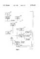
- FIG. 1is a block diagram of a computer system.
- FIG. 2is a block diagram of a peripheral control chip in the computer system.
- FIG. 3is a table showing the conditions under which a power-on password is blocked.
- FIG. 4is a schematic diagram of logic in the peripheral control chip.
- FIGS. 5A and 5Bare a table describing the bits in a security control register in the peripheral control chip.
- a computer system Cincludes a central processing unit (CPU) 100 that communicates with a Peripheral Component Interconnect (PCI) bus 104 through a CPU-PCI bridge 102, which may be implemented with PCMC 82434LX from Intel Corporation or a custom-designed ASIC.
- the PCI bus 104may be connected to a video card 106, which controls video signals to a monitor (not shown) such as a CRT monitor.
- the computer system Calso includes an expansion bus 110, such as the Industry Standard Architecture (ISA) bus, which communicates with the PCI bus 104 through a PCI-ISA bridge 108, such as the PIX3 82371SB from Intel Corporation or a customed-designed ASIC.
- ISAIndustry Standard Architecture
- the ISA bus 110is connected to peripheral devices, such as a super I/O chip 114 (which may be implemented with the PC87306VUL from National or the FDC37C931 from SMC), a peripheral control chip 112, and an ISA device 126.
- the super I/O chip 114controls access to the following devices: a flash ROM 116, which stores the BIOS code for controlling power-on functions of the computer system C; a floppy disk drive 118; a serial port 120 for connection to a device such as a mouse; and a parallel port 122 for connection to a device such as a printer.
- the super I/O chip 114is connected to the data, address and control portions of the ISA bus 110, but it does not receive the usual ISA address enable signal AEN.
- the super I/O chip 114also contains CMOS memory for storing CMOS configuration information as well as a power-on password to control user access to the computer system C.
- the peripheral control chip 112is also connected to the data, address and control portions of the ISA bus 110, including the address enable signal AEN.
- the AEN signalis negated low to enable either the super I/O chip 114 or the peripheral control chip 112 to decode an address on the ISA bus 110. Cycles in which the AEN signal is driven high include a direct memory access (DMA) cycle, an ISA bus master cycle, and a refresh cycle.
- DMAdirect memory access
- the peripheral control chip 112generates signals SIOAEN and SIOWC -- , which are the address enable and write command signals, respectively, to the super I/O chip 114.
- the peripheral control chip 112also generates a flash ROM write protect signal FRWP -- , which is active low to disable writes to the flash ROM 116.
- the peripheral control chip 112receives a floppy write protect signal FLWP -- from the floppy disk drive 118, and it generates a signal SIOFWP -- to the super I/O chip 114 for disabling writes to the floppy disk drive 118.
- the peripheral control chip 112contains a black box 200 having two slots: slot 0 and slot 1.
- Slot 0protects the flash ROM 116 from unauthorized writes by controlling the write protect signal FRWP -- .
- Slot 0unlocks the flash ROM protection mechanism only after a user enters a correct password, which is loaded by the system BIOS into slot 0 during power-up.
- the signal FRWP --is deasserted high at reset and is driven active low to protect the flash ROM after a password is written to slot 0 and a protect resources or permanently locked resources command is issued.
- Slot 1is used to prevent access to the power-on password used to control access to the computer system C. Slot 1 also allows the user to change the power-on password during computer run time, so the user does not have to power cycle the computer system C and go into computer setup while booting to change the password.
- the system BIOSprotects the power-on password by storing another password in slot 1 and issuing a protect resources command or a permanently locked resources command.
- the black box slot 1 and an access enable block 210control access to the power-on password stored in the super I/O chip 114 by driving the signal SIOAEN high, which prevents the super I/O chip 114 from responding to a bus cycle on the ISA bus 110.
- the contents of the black box 200are accessible through a command register 202 and a data/status register 204.
- the command register 202determines if slot 0 or slot 1 is accessed, and it also stores one of the following black box commands: read status, which loads the contents of slot 0 or 1 into the status register 204; store password, which loads the bytes in the data/status register 204 into slot 0 or 1; protect resources, which blocks access to slot 0 or 1 until the proper password is entered or the computer system C is power-cycled; access resources, which causes the bytes in the data/status register 204 to be compared with the stored password in slot 0 or 1 to determine if access should be allowed; and permanently locked resources, which blocks access to slot 0 or 1 until the computer system C is power cycled. To prevent unauthorized over-writing of slot 1, the copy of the password in slot 1 must be first entered before write access is allowed to slot 1.
- the data/status register 204is a read/write register (i.e., it is a data register on writes and a status register on reads). Data register 204 can be written with password bytes, for example, to store a password into slot 0 or slot 1. Status register 204 can be read to determine if slot 0 or 1 is in protect resources mode or permanently locked mode or if a time delay is in progress. A time delay, for example, a one-second delay, can be forced by the black box 200 if a password mismatch occurred.
- the peripheral control chip 112can also block read or write access to the CMOS configuration information stored in the CMOS memory of the super I/O chip 114 by driving the signal SIOAEN high. In addition, the peripheral control chip 112 can block writes to resources controlled by the super I/O chip 114, such as the serial port 120, parallel port 122, floppy disk drive 118, or the CMOS configuration information. To implement the security features, the peripheral control chip 112 includes an SIO -- PORT register 212, an SIO security control register 216, an SIO index address register 218, an SIO index data register 220, an SIO data address register 224, and SIO write block registers 226. An index address is written into a client management (CM) index register 230 to select one of the registers 216, 218, 220, 224 and 226, with the contents of the selected register programmed with data written to a CM data register 232.
- CMclient management
- the SIO security control register 216can be 8 bits wide and programmed according to Table 2 in FIGS. 5A and 5B.
- the SIO index address register 218holds the index address to the super I/O chip 114, which is the address that a configuration register index of the super I/O chip 114 is written to. If an I/O write on the ISA bus 110 contains an address that matches the contents of the index address register 218, the I/O write data, i.e., the current index of the super I/O chip 114, is stored into an SIO index data register 220.
- the SIO data address register 224stores the data address of the super I/O chip 114, which is the address that the configuration data of the super I/O chip 114 is written to or read from.
- Each of the SIO write block registers 226holds a super I/O configuration index that is blocked to implement such security features as disabling the serial port 120, parallel port 122, and floppy disk drive 118.
- the index address register 216, index data register 218, data address register 224, and write block register 226are programmable to different values to protect different index and address ranges.
- registers 216, 224 and 226are write-protectable by programming the SIO security control register, such as by setting bit 7 high. Thus, once the protected index and address ranges are set, access of the registers 216, 224 and 226 is disabled to prevent software, such as a virus program, from altering the contents of the registers.
- Table 1describes how the black box slot 1 controls read or write access to the power-on password stored in the super I/O chip 114.
- Two conditionscause the access enable block 210 to drive the signal SIOAEN high.
- the first conditionoccurs when slot 1 is in protect resources mode, the I/O bus address contains the data address of the super I/O chip 114, and the SIO -- PORT register 212 contains the index address of the power-on password.
- the second conditionis the same as the first condition except that slot 1 is in the permanently locked state.
- the signal SIOAENfollows the ISA bus address enable signal AEN.
- the block select decoder 214(FIG.
- the access enable block 210includes a 4-input OR gate 300 for generating the signal SIOAEN.
- the OR gate 300receives a signal BLOCKAEN, the ISA address enable signal AEN, a signal SIOBLOCKAEN, and the output of an AND gate 302.
- the AND gate 302receives signals UNLOCK -- and AENLOCK -- EN.
- the signal UNLOCK --is driven high in response to a protect resources command or a permanently locked resources command to the black box slot 1.
- the signal AENLOCK -- ENis driven high if an I/O cycle contains the data address of the super I/O chip 114 and the SIO -- PORT register 212 contains the power-on password data address.
- Driving both signals UNLOCK -- and AENLOCK -- EN highcauses the signal SIOAEN to be driven high to prevent access of the power-on password.
- the signal UNLOCK --is driven low if an access resources command is issued to the black box slot 1 with the correct password while slot 1 is in the protect resources mode.
- the signal SIOBLOCKAENis driven high by the block select decoder 214 to prevent access to CMOS configuration information stored in the super I/O chip 114.
- An AND gate 314 for generating the signal SIOBLOCKAENhas one input connected to the signal XA71 (data address of the super I/O chip 114) and the other input connected to the output of an AEN decoder 316.
- the AEN decoder 316receives the outputs of the SIO -- PORT register 212 and the SIO security control register 216.
- the signal SIOBLOCKAENis high if the signal XA71 is asserted, bit 3 of the SIO security register 216 is set high, and the SIO -- PORT register 212 contains a value as determined by bit 2 of the SIO security control register 216.
- An OR gate 306generates the signal SIOWC -- , which receives a signal IOWC -- MUXOUT (the ISA write command signal IOWC -- ) and the output of an AND gate 304.
- the AND gate 304receives a signal SIOBLOCKIOWC and the inverted state of a signal IOWC -- MUXSEL, which is used to block the SIOBLOCKIOWC path.
- the signal SIOBLOCKIOWCis asserted high by the block select decoder 214 to block writes to the CMOS configuration information in the super I/O chip 114.
- the block select decoder 214contains an OR gate 320 for generating the signal SIOBLOCKIOWC.
- the inputs of the OR gate 320receive the outputs of AND gates 310 and 322.
- One input of the AND gate 310is connected to the output of an IOWC decoder 312, and the other input receives the signal XA71.
- the IOWC decoder 312receives the output of the SIO -- PORT register 212 and the output of the SIO security control register 216.
- the signal SIOBLOCKIOWCis high if the signal XA71 is asserted, bit 5 of the SIO security control register 216 is set high, and the SIO -- PORT register 212 contains a value determined by the state of bit 4 of the SIO security control register 216.
- the AND gate 322receives bit 6 of the SIO security control register 216 (SIO-SEC 6!), a signal DATAADDRHIT for indicating that the ISA bus address is equal to the address in the SIO data address register 224, and a signal DATAMATCH for indicating that the data in the SIO index data register 220 matches the data in one of the SIO write block registers 226.
- a comparator 308To prevent aliasing of addresses between different I/O devices on the ISA bus 110, such as between the super I/O chip 114 and the ISA device 126, a comparator 308 generates the signal BLOCKAEN. For example, an I/O address of 70 h or 71 h is allocated to ports in the super I/O chip 114, which decodes only the 10 least significant address bits. However, the same ports will also respond to address values of 470 h, 471 h, 870 h, 871 h, C70 h or C71 h (i.e. upper two bits contains a non-zero value) presented on the ISA bus 110.
- Aliasingoccurs when more than one bus device responds to a bus address, resulting in bus contention, which may occur if at least one bus device decodes less than the total number of bus address bits.
- the first input of the comparator 308receives the ISA bus address signals SA 11:0!, and a second input receives the address alias values for comparison to the ISA bus address SA 11:0!. If the comparator 308 determines that an ISA bus address will cause an alias condition, i.e., the upper two ISA address bits SA 11:10! contains a non-zero value, it drives the signal BLOCKAEN high to disable SIOAEN.
- the index of the SIO security control register 216is first selected through the CM index register 230, followed by a read of the contents of the SIO security control register 216. The read allows the system software to determine the status of the control register 216. Next, bit 3 of the SIO security control register 216 is set high and bit 2 is set high or low depending on whether 4 or 8 bytes are to be locked.
- bit 5 of the SIO security control register 216is set high and bit 4 is set high or low depending on whether 192 or 144 bytes are locked.
- bit 1 of the SIO control register 216is set high.
- the following proceduremay be used.
- the index address register 218is selected and written with the index address of the disabled super I/O port.
- the SIO data address register 224is selected and written with the data address of the disabled super I/O port.
- the indexes of the enable bits in the super I/O chip 114 for the floppy disk drive 118, serial port 120, and parallel port 122are written into the SIO write block registers 226. This effectively prevents the enable bits from being set in the super I/O chip 114, which disables access to the floppy disk drive 118, the serial port 120, and the parallel port 122.
- the SIO security control register 216is selected and the contents of the register read.
- bits 7 and 6 of the SIO control register 216are set high. This effectively prevents the contents of the SIO security control register 216, the SIO index address register 218, and the SIO write block register 224 from being changed and disables the signal SIOWC -- .
- the computer system Ccan be configured without a PCI bus, the ISA bus can be replaced with a different expansion bus, and different types of I/O devices can be connected to the expansion bus.
Landscapes
- Engineering & Computer Science (AREA)
- Theoretical Computer Science (AREA)
- Computer Security & Cryptography (AREA)
- Physics & Mathematics (AREA)
- General Engineering & Computer Science (AREA)
- General Physics & Mathematics (AREA)
- Storage Device Security (AREA)
Abstract
Description
Claims (29)
Priority Applications (1)
| Application Number | Priority Date | Filing Date | Title |
|---|---|---|---|
| US08/638,143US5778199A (en) | 1996-04-26 | 1996-04-26 | Blocking address enable signal from a device on a bus |
Applications Claiming Priority (1)
| Application Number | Priority Date | Filing Date | Title |
|---|---|---|---|
| US08/638,143US5778199A (en) | 1996-04-26 | 1996-04-26 | Blocking address enable signal from a device on a bus |
Publications (1)
| Publication Number | Publication Date |
|---|---|
| US5778199Atrue US5778199A (en) | 1998-07-07 |
Family
ID=24558823
Family Applications (1)
| Application Number | Title | Priority Date | Filing Date |
|---|---|---|---|
| US08/638,143Expired - LifetimeUS5778199A (en) | 1996-04-26 | 1996-04-26 | Blocking address enable signal from a device on a bus |
Country Status (1)
| Country | Link |
|---|---|
| US (1) | US5778199A (en) |
Cited By (10)
| Publication number | Priority date | Publication date | Assignee | Title |
|---|---|---|---|---|
| US6032213A (en)* | 1997-09-11 | 2000-02-29 | Advanced Micro Devices, Inc. | PC core logic chipset comprising a serial register access bus |
| US6178478B1 (en)* | 1998-12-11 | 2001-01-23 | Vlsi Technology, Inc. | Smart target mechanism for eliminating dual address cycles in a peripheral component interconnect environment |
| US6301665B1 (en)* | 1998-04-30 | 2001-10-09 | Compaq Computer Corporation | Security methodology for devices having plug and play capabilities |
| US6490644B1 (en) | 2000-03-08 | 2002-12-03 | International Business Machines Corporation | Limiting write data fracturing in PCI bus systems |
| US20030084285A1 (en)* | 2001-10-26 | 2003-05-01 | International Business Machines Corporation | Method and system for detecting a tamper event in a trusted computing environment |
| US6591320B1 (en)* | 1999-06-01 | 2003-07-08 | International Business Machines Corporation | Method and system for selective disablement of expansion bus slots in a multibus data processing system |
| US7069404B1 (en)* | 1999-01-11 | 2006-06-27 | Stmicroelectronics Sa | Microprocessor with protection circuits to secure the access to its registers |
| US20070150682A1 (en)* | 2005-12-05 | 2007-06-28 | Naruhiko Ogasawara | Data processing apparatus maintaining consistency of operation |
| US20070168582A1 (en)* | 2005-09-07 | 2007-07-19 | Chao-Chen Huang | Method for protecting an i/o port of a computer |
| US20090222909A1 (en)* | 2008-02-29 | 2009-09-03 | Lenovo (Singapore) Pte. Ltd | Password Management Outside of a Bios |
Citations (18)
| Publication number | Priority date | Publication date | Assignee | Title |
|---|---|---|---|---|
| US4446475A (en)* | 1981-07-10 | 1984-05-01 | Motorola, Inc. | Means and method for disabling access to a memory |
| US4941089A (en)* | 1986-12-12 | 1990-07-10 | Datapoint Corporation | Input/output network for computer system |
| US4959860A (en)* | 1989-02-07 | 1990-09-25 | Compaq Computer Corporation | Power-on password functions for computer system |
| US4961172A (en)* | 1988-08-11 | 1990-10-02 | Waferscale Integration, Inc. | Decoder for a memory address bus |
| US5097445A (en)* | 1989-03-03 | 1992-03-17 | Mitsubishi Denki Kabushiki Kaisha | Semiconductor integrated circuit with selective read and write inhibiting |
| US5101492A (en)* | 1989-11-03 | 1992-03-31 | Compaq Computer Corporation | Data redundancy and recovery protection |
| US5287519A (en)* | 1992-09-17 | 1994-02-15 | International Business Machines Corp. | LAN station personal computer system with controlled data access for normal and unauthorized users and method |
| US5319767A (en)* | 1992-06-29 | 1994-06-07 | The United States Of America As Represented By The Secretary Of The Navy | Slave controller for effecting a block transfer of sixteen bit words between a memory and a data transfer bus |
| US5375243A (en)* | 1991-10-07 | 1994-12-20 | Compaq Computer Corporation | Hard disk password security system |
| US5388156A (en)* | 1992-02-26 | 1995-02-07 | International Business Machines Corp. | Personal computer system with security features and method |
| US5396602A (en)* | 1993-05-28 | 1995-03-07 | International Business Machines Corp. | Arbitration logic for multiple bus computer system |
| US5454081A (en)* | 1992-08-28 | 1995-09-26 | Compaq Computer Corp. | Expansion bus type determination apparatus |
| US5500949A (en)* | 1990-03-27 | 1996-03-19 | Kabushiki Kaisha Toshiba | Microprocessor system for inhibiting access to memory by checking specific address and specific codes |
| US5513337A (en)* | 1994-05-25 | 1996-04-30 | Intel Corporation | System for protecting unauthorized memory accesses by comparing base memory address with mask bits and having attribute bits for identifying access operational mode and type |
| US5522086A (en)* | 1993-10-29 | 1996-05-28 | Sierra Semiconductor Canada, Inc. | Software configurable ISA bus card interface with security access read and write sequence to upper data bits at addresses used by a game device |
| US5579490A (en)* | 1987-08-17 | 1996-11-26 | Nec Corporation | Expanded address bus system |
| US5596727A (en)* | 1993-06-02 | 1997-01-21 | Lucent Technologies Inc. | Arrangement for expanding the device capacity of a bus |
| US5654650A (en)* | 1995-12-11 | 1997-08-05 | Hewlett-Packard Company | High throughput FPGA control interface |
- 1996
- 1996-04-26USUS08/638,143patent/US5778199A/ennot_activeExpired - Lifetime
Patent Citations (18)
| Publication number | Priority date | Publication date | Assignee | Title |
|---|---|---|---|---|
| US4446475A (en)* | 1981-07-10 | 1984-05-01 | Motorola, Inc. | Means and method for disabling access to a memory |
| US4941089A (en)* | 1986-12-12 | 1990-07-10 | Datapoint Corporation | Input/output network for computer system |
| US5579490A (en)* | 1987-08-17 | 1996-11-26 | Nec Corporation | Expanded address bus system |
| US4961172A (en)* | 1988-08-11 | 1990-10-02 | Waferscale Integration, Inc. | Decoder for a memory address bus |
| US4959860A (en)* | 1989-02-07 | 1990-09-25 | Compaq Computer Corporation | Power-on password functions for computer system |
| US5097445A (en)* | 1989-03-03 | 1992-03-17 | Mitsubishi Denki Kabushiki Kaisha | Semiconductor integrated circuit with selective read and write inhibiting |
| US5101492A (en)* | 1989-11-03 | 1992-03-31 | Compaq Computer Corporation | Data redundancy and recovery protection |
| US5500949A (en)* | 1990-03-27 | 1996-03-19 | Kabushiki Kaisha Toshiba | Microprocessor system for inhibiting access to memory by checking specific address and specific codes |
| US5375243A (en)* | 1991-10-07 | 1994-12-20 | Compaq Computer Corporation | Hard disk password security system |
| US5388156A (en)* | 1992-02-26 | 1995-02-07 | International Business Machines Corp. | Personal computer system with security features and method |
| US5319767A (en)* | 1992-06-29 | 1994-06-07 | The United States Of America As Represented By The Secretary Of The Navy | Slave controller for effecting a block transfer of sixteen bit words between a memory and a data transfer bus |
| US5454081A (en)* | 1992-08-28 | 1995-09-26 | Compaq Computer Corp. | Expansion bus type determination apparatus |
| US5287519A (en)* | 1992-09-17 | 1994-02-15 | International Business Machines Corp. | LAN station personal computer system with controlled data access for normal and unauthorized users and method |
| US5396602A (en)* | 1993-05-28 | 1995-03-07 | International Business Machines Corp. | Arbitration logic for multiple bus computer system |
| US5596727A (en)* | 1993-06-02 | 1997-01-21 | Lucent Technologies Inc. | Arrangement for expanding the device capacity of a bus |
| US5522086A (en)* | 1993-10-29 | 1996-05-28 | Sierra Semiconductor Canada, Inc. | Software configurable ISA bus card interface with security access read and write sequence to upper data bits at addresses used by a game device |
| US5513337A (en)* | 1994-05-25 | 1996-04-30 | Intel Corporation | System for protecting unauthorized memory accesses by comparing base memory address with mask bits and having attribute bits for identifying access operational mode and type |
| US5654650A (en)* | 1995-12-11 | 1997-08-05 | Hewlett-Packard Company | High throughput FPGA control interface |
Cited By (12)
| Publication number | Priority date | Publication date | Assignee | Title |
|---|---|---|---|---|
| US6032213A (en)* | 1997-09-11 | 2000-02-29 | Advanced Micro Devices, Inc. | PC core logic chipset comprising a serial register access bus |
| US6301665B1 (en)* | 1998-04-30 | 2001-10-09 | Compaq Computer Corporation | Security methodology for devices having plug and play capabilities |
| US6178478B1 (en)* | 1998-12-11 | 2001-01-23 | Vlsi Technology, Inc. | Smart target mechanism for eliminating dual address cycles in a peripheral component interconnect environment |
| US7069404B1 (en)* | 1999-01-11 | 2006-06-27 | Stmicroelectronics Sa | Microprocessor with protection circuits to secure the access to its registers |
| US6591320B1 (en)* | 1999-06-01 | 2003-07-08 | International Business Machines Corporation | Method and system for selective disablement of expansion bus slots in a multibus data processing system |
| US6490644B1 (en) | 2000-03-08 | 2002-12-03 | International Business Machines Corporation | Limiting write data fracturing in PCI bus systems |
| US20030084285A1 (en)* | 2001-10-26 | 2003-05-01 | International Business Machines Corporation | Method and system for detecting a tamper event in a trusted computing environment |
| US7490250B2 (en) | 2001-10-26 | 2009-02-10 | Lenovo (Singapore) Pte Ltd. | Method and system for detecting a tamper event in a trusted computing environment |
| US20070168582A1 (en)* | 2005-09-07 | 2007-07-19 | Chao-Chen Huang | Method for protecting an i/o port of a computer |
| US20070150682A1 (en)* | 2005-12-05 | 2007-06-28 | Naruhiko Ogasawara | Data processing apparatus maintaining consistency of operation |
| US20090222909A1 (en)* | 2008-02-29 | 2009-09-03 | Lenovo (Singapore) Pte. Ltd | Password Management Outside of a Bios |
| US8566600B2 (en)* | 2008-02-29 | 2013-10-22 | Lenovo (Singapore) Pte. Ltd. | Password management outside of a BIOS |
Similar Documents
| Publication | Publication Date | Title |
|---|---|---|
| KR100298620B1 (en) | System for controlling access to a register mapped to an i/o address space of a computer system | |
| US7149854B2 (en) | External locking mechanism for personal computer memory locations | |
| US7917716B2 (en) | Memory protection for embedded controllers | |
| EP3814969B1 (en) | Peripheral access on a secure-aware bus system | |
| US4388695A (en) | Hardware memory write lock circuit | |
| US5199032A (en) | Microcontroller having an EPROM with a low voltage program inhibit circuit | |
| US6397337B1 (en) | Unified password prompt of a computer system | |
| US5970246A (en) | Data processing system having a trace mechanism and method therefor | |
| EP0382468A2 (en) | Power-on password functions for computer system | |
| US6832320B1 (en) | Ownership tag on power-up screen | |
| EP3814960B1 (en) | Secure-aware bus system | |
| US11537762B2 (en) | Secure peripheral interconnect | |
| US5778199A (en) | Blocking address enable signal from a device on a bus | |
| US6542995B2 (en) | Apparatus and method for maintaining secured access to relocated plug and play peripheral devices | |
| US6920566B2 (en) | Secure system firmware by disabling read access to firmware ROM | |
| WO2008030727A2 (en) | Access control of memory space in microprocessor systems | |
| US6301665B1 (en) | Security methodology for devices having plug and play capabilities | |
| US7054121B2 (en) | Protection circuit for preventing unauthorized access to the memory device of a processor | |
| JP4799822B2 (en) | System and method for controlling access between devices in a computer system | |
| JP7079558B2 (en) | Safety device for SPI flash | |
| US20080034150A1 (en) | Data processing circuit | |
| KR20000009381A (en) | Memory writing protection apparatus of computer system | |
| JPH04160583A (en) | Single-chip microcomputer | |
| JPH01261760A (en) | computer equipment | |
| JPH0399347A (en) | Semiconductor integrated circuit devices and password methods |
Legal Events
| Date | Code | Title | Description |
|---|---|---|---|
| AS | Assignment | Owner name:COMPAQ COMPUTER CORPORATION, TEXAS Free format text:ASSIGNMENT OF ASSIGNORS INTEREST;ASSIGNORS:WANNER, CHRISTOPHER C.;WOODS, ROBERT L.;REEL/FRAME:008054/0685;SIGNING DATES FROM 19960425 TO 19960426 | |
| FEPP | Fee payment procedure | Free format text:PAYOR NUMBER ASSIGNED (ORIGINAL EVENT CODE: ASPN); ENTITY STATUS OF PATENT OWNER: LARGE ENTITY | |
| STCF | Information on status: patent grant | Free format text:PATENTED CASE | |
| FPAY | Fee payment | Year of fee payment:4 | |
| AS | Assignment | Owner name:COMPAQ INFORMATION TECHNOLOGIES GROUP, L.P., TEXAS Free format text:ASSIGNMENT OF ASSIGNORS INTEREST;ASSIGNOR:COMPAQ COMPUTER CORPORATION;REEL/FRAME:012418/0222 Effective date:20010620 | |
| AS | Assignment | Owner name:HEWLETT-PACKARD DEVELOPMENT COMPANY, L.P., TEXAS Free format text:CHANGE OF NAME;ASSIGNOR:COMPAQ INFORMATION TECHNOLOGIES GROUP, LP;REEL/FRAME:015000/0305 Effective date:20021001 | |
| FPAY | Fee payment | Year of fee payment:8 | |
| FPAY | Fee payment | Year of fee payment:12 |