US5778194A - Method and apparatus for measuring performance of a computer bus - Google Patents
Method and apparatus for measuring performance of a computer busDownload PDFInfo
- Publication number
- US5778194A US5778194AUS08/629,154US62915496AUS5778194AUS 5778194 AUS5778194 AUS 5778194AUS 62915496 AUS62915496 AUS 62915496AUS 5778194 AUS5778194 AUS 5778194A
- Authority
- US
- United States
- Prior art keywords
- bus
- signal
- counter
- clock cycles
- time period
- Prior art date
- Legal status (The legal status is an assumption and is not a legal conclusion. Google has not performed a legal analysis and makes no representation as to the accuracy of the status listed.)
- Expired - Lifetime
Links
Images


Classifications
- G—PHYSICS
- G06—COMPUTING OR CALCULATING; COUNTING
- G06F—ELECTRIC DIGITAL DATA PROCESSING
- G06F11/00—Error detection; Error correction; Monitoring
- G06F11/30—Monitoring
- G06F11/34—Recording or statistical evaluation of computer activity, e.g. of down time, of input/output operation ; Recording or statistical evaluation of user activity, e.g. usability assessment
- G06F11/3466—Performance evaluation by tracing or monitoring
- G06F11/349—Performance evaluation by tracing or monitoring for interfaces, buses
- G—PHYSICS
- G06—COMPUTING OR CALCULATING; COUNTING
- G06F—ELECTRIC DIGITAL DATA PROCESSING
- G06F11/00—Error detection; Error correction; Monitoring
- G06F11/30—Monitoring
- G06F11/34—Recording or statistical evaluation of computer activity, e.g. of down time, of input/output operation ; Recording or statistical evaluation of user activity, e.g. usability assessment
- G06F11/3409—Recording or statistical evaluation of computer activity, e.g. of down time, of input/output operation ; Recording or statistical evaluation of user activity, e.g. usability assessment for performance assessment
- G—PHYSICS
- G06—COMPUTING OR CALCULATING; COUNTING
- G06F—ELECTRIC DIGITAL DATA PROCESSING
- G06F2201/00—Indexing scheme relating to error detection, to error correction, and to monitoring
- G06F2201/87—Monitoring of transactions
- G—PHYSICS
- G06—COMPUTING OR CALCULATING; COUNTING
- G06F—ELECTRIC DIGITAL DATA PROCESSING
- G06F2201/00—Indexing scheme relating to error detection, to error correction, and to monitoring
- G06F2201/88—Monitoring involving counting
Definitions
- the present inventionrelates generally to a bus monitoring device, and more particularly to a monitoring device which facilitates determining I/O (Input/Output) bus performance characteristics such as the utilization or efficiency of an I/O bus relative to a peripheral device.
- I/OInput/Output
- PCI Local Busis a known high performance, 32-bit or 64-bit I/O bus with multiplexed address and data lines. It is intended for use as an interconnect mechanism between highly integrated peripheral controller components, peripheral add-in boards, and processor/memory systems.
- a PCI Local Bus standardis defined in the document entitled PCI Local Bus Specification, Revision 2.1 which is available from the PCI Special Interest Group, P.O. Box 14070, Portland, Oreg. 97214, and which is incorporated herein by reference.
- a SCSI (Small Computer System Interface) busis a known I/O bus which is used for connecting computers to peripheral devices, such as hard disks and printers. That is, a SCSI bus is typically an external and lower speed I/O bus which is primarily used for connecting peripheral devices to a higher speed system I/O bus such as a PCI Local Bus.
- a SCSI standardis defined by the X3T9.2 committee of the American National Standards Institute (ANSI).
- the first version of the standard, SCSI-1is described in ANSI Document No. X3.131-1986 which is incorporated herein by reference.
- the SCSI-1 specificationhas been upgraded with an expanded interface referred to as SCSI-2.
- the SCSI-2 specificationis described in ANSI Document No. X3.131-1994 which is also incorporated herein by reference.
- the ANSI committeeis presently working on a SCSI-3 specification.
- I/O bussuch as a PCI Local Bus or a SCSI bus
- a peripheral devicesuch as a peripheral controller component or a peripheral add-in board that is connected to the I/O bus. That is, there appears to be no simple and cost effective tool for measuring or otherwise determining the utilization or efficiency of an I/O bus during I/O bus transactions involving a particular peripheral device, either during a product development phase, or in an end-user environment.
- a method for measuring performance of an I/O busincludes the steps of (a) determining a number of I/O bus clock cycles that occur during I/O bus transactions involving a peripheral device during a time period, and (b) determining a bus performance value for the I/O bus based on the number of I/O bus clock cycles determined in step (a).
- an apparatus for measuring performance of an I/O busincludes a counter connected to the I/O bus for counting a number of I/O bus clock cycles that occur during I/O bus transactions involving a peripheral device during a time period, and a mechanism for determining a bus utilization value for the I/O bus based on the number of I/O bus clock cycles counted by the counter.
- an apparatus for measuring performance of an I/O busincludes a counter connected to the I/O bus for counting a number of I/O bus clock cycles that occur during data transfers involving the peripheral device during the time period, and a mechanism for determining a bus efficiency value for the I/O bus based on the number of I/O bus clock cycles counted by the counter.
- FIG. 1is a block diagram of a first embodiment of a computer system architecture which incorporates the features of the present invention therein;
- FIG. 2is a block diagram of a bus monitoring apparatus shown in FIG. 1;
- FIG. 3is a block diagram of showing an exemplary interface between a PCI compliant device and a PCI Local Bus;
- FIG. 4is a timing diagram for a basic read transaction across a PCI Local Bus
- FIG. 5is a timing diagram for a basic write transaction across a PCI Local Bus
- FIG. 6is a state machine diagram for determining PCI Local Bus utilization
- FIG. 7is a state machine diagram for determining PCI Local Bus efficiency
- FIG. 8is a block diagram of a second embodiment of a computer system architecture which incorporates the features of the present invention therein;
- FIG. 9is a block diagram of a third embodiment of a computer system architecture which incorporates the features of the present invention therein.
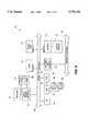
- the computer system architecture 10may include a processor 12, cache 14, bridge/memory controller 16, DRAM (Dynamic Random Access Memory) 18, I/O (Input/Output) bus 20 such as a PCI Local Bus, a Micro-Channel bus or any high speed I/O system bus, and a number of peripheral devices.
- the computer system architecture 10may include a number of peripheral add-in boards or cards such as audio card 22, motion video card 24 and graphics card 26, a number of controllers such as LAN host adapter 28 and SCSI host adapter 30, and an expansion bus interface 32.
- a display monitor 34may be operatively connected to the graphics card 26.
- One or more known disk drives 36may be connected to the SCSI host adapter 30. It should be appreciated that the host adapter 30 may conform with data transfer protocols other than SCSI, for instance IDE (Integrated Device Electronics), FDDI (Fiber Distributed Data Interface), SSA (Serial Storage Architecture), or Fibre Channel.
- the expansion bus interface 32may interface an expansion bus 38 such as an ISA (Industry Standard Architecture), or EISA (Extended Industry Standard Architecture) bus to the I/O bus 20.
- the processor 12, cache 14 and DRAM 18are connected to the I/O bus 20 through the bridge/memory controller 16 which provides a low latency path through which the processor 12 may directly access the peripheral devices that are mapped in memory or I/O address spaces.
- the bridge/memory controller 16also provides a path which permits the peripheral devices to directly access the DRAM 18.
- the computer system architecture 10also includes a bus monitoring apparatus 40.
- the bus monitor 40monitors a particular peripheral device for a predetermined amount of time to determine the effectiveness of bus transactions across the I/O bus 20 relative to the particular peripheral device.
- the effectiveness of I/O bus transactionsmay be measured in performance terms such as bus utilization, or bus efficiency.
- the bus monitor 40facilitates quantifying the utilization or efficiency of the I/O bus 20 with regard to a particular peripheral device.
- bus utilizationis defined as a ratio of the total number of clock cycles used for bus transactions across the I/O bus during a predetermined time period or interval, to the total number of clock cycles available for bus transactions across the I/O bus during the predetermined time interval.
- bus efficiencyis defined as a ratio of the total number of clock cycles used for transferring data across the I/O bus 20 during a predetermined time period or interval, to the total number of clock cycles used for bus transactions across the I/O bus during the predetermined time interval.
- bus utilization and bus efficiencymay be defined differently depending upon the particular specifications of the I/O bus being monitored.
- state machine(s)by changing the state machine(s), other I/O bus performance characteristics may be monitored.
- the bus monitor 40is associated with the SCSI host adapter 30.
- the bus monitor 40may be associated with other types of peripheral devices, such as audio card 22, motion video card 24 or graphics card 26, or associated with any other type of controller such as LAN host adapter 28.
- the bus monitor 40may stand alone as a separate integrated circuit mounted on a circuit board of the particular peripheral or controller with which it is associated.
- the bus monitor 40may be integrated with other circuitry into an integrated circuit forming at least a portion of the particular peripheral or controller with which it is associated.
- the bus monitor 40 of the present inventionwill hereafter be discussed relative to a particular I/O bus implementation such as a PCI Local Bus 20, and a particular peripheral device such as the SCSI host adapter 30.
- the bus monitor 40may operate with different types of I/O buses such as a SCSI bus, and the bus monitor 40 may be associated with different types of peripheral devices as enumerated above.
- the bus monitor 40includes logic such as a decoder 42, one or more state machines 44, a counter 46 and a number of tri-state drivers 48.
- the bus monitor logicmay be interfaced to the PCI Local Bus 20 through a number of known PCI Local Bus drivers/receivers 50.
- the PCI Local Bus signalsare distributed to the bus monitor logic through a number of signal lines 52.
- the decoder 42performs various tasks in response to instructions which are decoded from the PCI Local Bus address signals on lines 52. As described in detail below, the decoder 42 performs tasks such as (1) reconfiguring the state machine(s) 44 so that the bus monitor 40 can monitor various user-specified events; (2) resetting the counter 46 after a monitoring operation has been completed; and (3) enabling the tri-state drivers 48 to permit the contents of the counter 46 to be read out of the counter 46 and onto the PCI Local Bus 20.
- a bus monitoring software utility(described below) that is executing on the host processor 12 may measure or otherwise determine the utilization or efficiency of the PCI Local Bus 20 relative to the PCI compliant device 30, based at least in part on the contents of the counter 46.
- the state machine(s) 44are selected based on the particular bus transaction events to be monitored.
- the state machine(s) 44monitor particular PCI Local Bus signals on lines 52, and enable/disable the counter 46 in response to the presence or absence of the particular PCI Local Bus signals on lines 52.
- the counter 46When enabled by the state machine(s) 44, the counter 46 is clocked by a PCI Local Bus clock (CLK) signal on an input line 53.
- CLKPCI Local Bus clock
- the counter 46will count each CLK signal on input line 53 when enabled by the state machine(s) 44, and will stop counting each CLK signal on input line 53 when disabled by the state machine(s) 44.
- the resulting count value (bit count) stored in the counter 46is useful in determining or measuring different bus performance characteristics depending upon the monitoring criteria embodied or implemented by the particular state machine 44 that is controlling the counter 46.
- the count value in the counter 46may represent the total number of PCI clock cycles associated with all data transfers initiated by the particular PCI compliant device, such as the SCSI host adapter 30.
- the counter 46may be a large (32 to 64 bit) counter.
- the PCI Local Bus 30nominally operates at clock frequencies up to 33 MHz, or at 66 MHz. At 33 MHz, a 32-bit counter should be able to count PCI clocks for approximately 130 seconds before overflowing. At 66 MHz, a 32-bit counter should be able to count PCI clocks for approximately 65 seconds before overflowing.
- the counter 64may be embodied as a small high speed 2 or 4-bit prescaling counter followed by additional slower speed ripple counter stages. This alternative embodiment would be primarily useful with high speed PCI Local Bus implementations.
- the bus monitor 40may also include a second counter circuit 54 which may be enabled/disabled (started/stopped) and reset by the decoder 42.
- the bus monitor software utilitythat is executing on the processor 12 may measure or otherwise determine the utilization or efficiency of the PCI Local Bus 20 relative to the PCI compliant device 30, based at least in part on the contents of the counter 54.
- the contents of the counter 54may be accessed by the host processor 12 via the PCI Local Bus 20 in the same manner as described above with regard to the contents of the counter 46. That is, one or more tri-state drivers 56 may be enabled by the decoder 42 to permit the contents of the counter 54 to be read onto the PCI Local Bus 20.
- the counter 54may be clocked by the PCI Local Bus clock (CLK) signal on the input line 53. Thus, the counter 54 begins counting each . CLK signal that occurs on input line 53 when enabled by the decoder 42, and continues counting CLK signals on input line 53 until disabled by the decoder 42.
- CLKPCI Local Bus clock
- the resulting count value (bit count) stored in the counter 54is useful in determining or measuring different bus performance characteristics as described further below.
- the counter 46 and/or the counter 54have bit counts that are larger than the PCI Local Bus 20 (i.e. 64-bit counter and 32-bit PCI Local Bus), then the resulting count value or timer value must be read out of the respective counter or timer and onto the PCI Local Bus in more than one step or operation.
- the counter 54may be replaced with a timer algorithm that executes as part of the bus monitor software utility.
- the bus monitor software utilitymay utilize a conventional computer system real time clock (not shown) to determine or otherwise calculate the total number of clock cycles occurring during a time period. It should be appreciated that the total number of clock cycles occurring during a given time period may be determined by multiplying the frequency of the I/O bus (cycles/second) by the time period (seconds).
- FIG. 3is a block diagram showing an exemplary interface between a PCI compliant peripheral device such as host adapter 30 and the signal lines 52 that define the PCI Local Bus 20. It should be appreciated that the PCI compliant device 30 must be capable of interfacing with required PCI Local Bus signals 52a, and may include the capability of interfacing with optional PCI Local Bus signals 52b.
- the following discussionrelates to basic transfer control across the PCI Local Bus 20.
- the fundamentals of all PCI Local Bus transfersare controlled with three signals, namely the cycle frame (FRAME#) signal 58 (FIG. 3), initiator ready (IRDY#) signal 60 (FIG. 3), and target ready (TRDY#) signal 62 (FIG. 3).
- the FRAME# signal 58is driven by a bus master to indicate the beginning and end of a PCI Local Bus transaction. More particularly, the FRAME# signal 58 is driven by a bus master to indicate the beginning and duration of a bus transaction.
- the FRAME# signal 58is asserted to indicate a bus transaction is beginning. While the FRAME# signal 58 is asserted, data transfers continue. When the FRAME# signal 58 is deasserted, a bus transaction is in a final data phase or has completed.
- the IRDY# signal 60is driven by the bus master to indicate that the bus master is ready to transfer data. That is, the IRDY# signal 60 indicates that the initiating agent (bus master) has the ability to complete the current data phase of the transaction.
- the IRDY# signal 60is used in conjunction with TRDY# signal 62.
- a data phaseis completed (i.e. data is transferred across the PCI Local Bus) on any clock where both the IRDY# signal 60 and the TRDY# signal 62 are both asserted.
- IRDY# signal 60indicates that valid data is present on the PCI Local Bus multiplexed address and data lines 64 (FIG. 3).
- IRDY# signal 60indicates that the bus master is prepared to accept data. Wait cycles (discussed further below) are inserted until both IRDY# signal 60 and TRDY# signal 62 are asserted together.
- the TRDY# signal 62is driven by the target device to indicate that it is ready to transfer data. More particularly, the TRDY# signal 62 indicates that the target agent (selected device) has the ability to complete the current data phase of the transaction. As previously mentioned, the TRDY# signal 62 is used in conjunction with the IRDY# signal 60. A data phase is completed on any clock that both TRDY# signal 62 and IRDY# signal 60 are asserted. During a read transaction, the TRDY# signal 62 indicates that valid data is present on the PCI Local Bus address lines 64. During a write transaction, the TRDY# signal 62 indicates that the target device is prepared to accept data. Wait cycles are inserted until both IRDY# signal 60 and TRDY# signal 62 are asserted together.
- the interface between the bus master device and the target deviceis in an idle state when both FRAME# signal 58 and IRDY# signal 60 are deasserted (high).
- the first clock edge on which FRAME# signal 58 is assertedis referred to as the address phase of the bus transaction. Address and bus command code information is transferred on the first clock edge defining the address phase.
- the next clock edgebegins the first of one or more data phases during which data is transferred between the master device and the target device on each clock edge for which both IRDY# signal 60 and TRDY# signal 62 are asserted (low). Wait cycles may be inserted in a data phase by either the master device or the target device when either the IRDY# signal 60 or the TRDY# signal 62 is deasserted (driven high).
- PCI Local Bus transactionsrequire at least two additional signals, namely the PCI clock (CLK) signal 66 (FIG. 3) and a grant (GNT#) signal 68 (FIG. 3).
- CLKPCI clock
- GNT#grant
- the CLK signal 66provides timing for all transactions on the PCI Local Bus 20 and is an input to every PCI compliant device or agent.
- the GNT# signal 68is an arbitration signal that indicates to the PCI compliant device, that access to the PCI Local Bus 20 has been granted by an arbiter in response to a request (REQ#) signal 69 asserted by the PCI compliant device when seeking access to the PCI Local Bus 20.
- REQ#request
- the GNT# signal 68is a point-to-point signal. That is, every PCI compliant device has its own GNT# signal line. Once the GNT# signal 68 is issued by the arbiter, the PCI compliant device is granted temporary "ownership" or control of the PCI Local Bus 20. In other words, the PCI compliant device is the only device which may access the PCI Local Bus 20 during the time period that the particular PCI compliant device's GNT# signal 68 is asserted.
- FIGS. 4 and 5there is shown a timing diagram for a basic read transaction across the PCI Local Bus 20, and a timing diagram for a basic write transaction across the PCI Local Bus 20, respectively.
- a signalWhen a signal is drawn as a solid line, it is actively being driven by the current bus master or target device. When a signal is drawn as a dashed line, no agent is actively driving the signal.
- the read transactionbegins with an address phase.
- the address phaseoccurs when a bus master asserts the FRAME# signal for the first time (clock 2).
- the multiplexed address and data lines (AD) 64contain a valid address
- the control/byte enable (C/BE#) linescontain a valid bus command.
- the first clock of the first data phaseis clock 3. It should be noted that the first data phase on a read transaction requires a turnaround-cycle (as indicated by the double arrows on the AD lines 64 during clock 3) which is enforced by the target device by deasserting the TRDY# signal 62
- the C/BE# linesindicate which byte lanes (a 32-bit data bus has 4 byte lanes available for transferring data) are involved in the current data phase.
- a data phasemay consist of wait cycles and a data transfer. Data is successfully transferred on clocks 4, 6 and 8, and wait cycles are inserted on clocks 3, 5 and 7.
- the first data phasecompletes in the minimum time for a read transaction because no wait states were asserted by either the initiator device or the target device.
- the second data phaseis extended on clock 5 because the TRDY# signal 62 is deasserted.
- the last data phaseis extended because the IRDY# signal 60 is deasserted on clock 7.
- the bus masterknows at clock 7 that the next data phase is the last data phase.
- FRAME# signal 58stays asserted. Only when the IRDY# signal 60 is asserted can the FRAME# signal 58 be deasserted, as occurs on clock 8, indicating to the target device that this is the last data phase of the transaction.
- a write transactionbegins when the FRAME# signal 58 is asserted for the first time, which occurs on clock 2.
- the data phaseswork the same way for both read and write transactions.
- the first and second data phasescomplete with zero wait cycles.
- the third data phasehas three wait cycles inserted by the target device, the first of which is inserted or requested by both the initiator device and the target device. That is, both the bus master and the target device insert wait cycles on clock 5.
- the IRDY# signal 60must be asserted when the FRAME# signal 58 is deasserted indicating the last data phase.
- the data transferis delayed by the bus master on clock 5 because the IRDY# signal 60 is deasserted.
- the last data phaseis signaled by the master on clock 6, but it does not complete until clock 8.
- FIG. 6there is shown a state diagram for a state machine 70 which facilitates determining or measuring the utilization of the PCI Local Bus 20 relative to the PCI compliant device 30.
- the state machine 70monitors a number of particular PCI Local Bus signals, namely, GNT# signal 68, FRAME# signal 58, and IRDY# signal 60, to determine whether to enable or disable the counter 46 (FIG. 2) during one or more bus transactions that occur during a predetermined test period.
- the state machine 70monitors the GNT# signal 68 for an assertion by a PCI arbiter device (not shown). As previously mentioned, an asserted GNT# signal 68 indicates that the arbiter device has granted the PCI compliant device 30 access to the PCI local Bus 20 during the next bus transaction. Thus, during the next bus transaction, the PCI compliant device 30 acts as a bus master. Once the GNT# signal 68 has been asserted, the state machine 70 transitions to state (0). While in state (0), the state machine 70 monitors the FRAME# signal 58 for an assertion by the bus master.
- the assertion of the FRAME# signal 58indicates the beginning of a PCI Local Bus transaction as previously described.
- the state machineadvances to state (1) and enables the counter 46 to begin counting CLK signals 66 on the input line 53 (FIG. 2).
- the state machine 70monitors the FRAME# signal 58 for a deassertion by the bus master while the counter 46 continues to count each CLK signal 66 on the input line 53.
- the deassertion of the FRAME# signal 58indicates that the next data phase will be the last data phase of the PCI Local Bus transaction, as previously described.
- the state machine 70advances to state (2). While in state (2), the state machine 70 monitors the IRDY# signal 60 for a deassertion (not IRDY#) by the initiator device. Once the IRDY# signal 60 is deasserted, the last data phase has completed, and the PCI Local Bus transaction has completed. Thus, the state machine 70 advances to state (3) and disables the counter 46 to prevent the counter 46 from counting any more CLK signals 66 on the input line 53 (FIG. 2). While in state (3), the state machine 70 monitors the GNT# signal 68 to detect when the next bus transaction involving the particular PCI compliant device will begin.
- the resulting count value in the counter 46represents the total number of PCI clock cycles required for the address phase, data phase(s) and wait cycles that comprise a typical PCI Local Bus transaction.
- the utilization of the PCI Local Bus 20 by the PCI compliant device 30may be measured or determined by dividing the count value in the counter 46 by the clock frequency of the PCI Local Bus 20 (typically 33 MHz), and then dividing the result by the total elapsed time of the test period (such as five or ten seconds). As previously mentioned, the test period may be timed the bus monitor software utility using the host computer real time clock.
- the utilization of the PCI local Bus 20 by the PCI compliant device 30may also be measured or determined by dividing the count value in the counter 46 by the count value in the counter 54 (FIG. 3). As previously mentioned, the count value in the counter 54 represents the total number of PCI clocks that occurred during the test period. It should be appreciated that a figure of merit indicative of the PCI Local Bus utilization by the PCI compliant device may be determined or calculated as described above by the bus monitoring software utility executing on the host processor 12.
- FIG. 7there is shown a diagram for state machine 80 which facilitates determining or measuring the efficiency of the PCI Local Bus 20 relative to the PCI compliant device 30.
- the state machine 80facilitates determining how efficiently the PCI Local Bus 20 operates during one or more bus transactions involving a particular PCI compliant device during a predetermined test period.
- the state machine 80monitors a number of particular PCI Local Bus signals, namely, GNT# signal 68, FRAME# signal 58, IRDY# signal 60, and TRDY# signal 62, to determine whether to enable or disable the counter 46 (FIG. 2).
- the state machine 80monitors the GNT# signal 68 for an assertion by a PCI arbiter device. Once the GNT# signal 68 has been asserted, the state machine 80 transitions to state (0). While in state (0), the state machine 80 monitors the FRAME# signal 58 for an assertion by the bus master. Once the FRAME# signal 58 is asserted, the state machine 80 advances to state (1) and monitors both the IRDY# signal 60 and the TRDY# signal 62 to detect when both signals are asserted. Once the state machine 80 detects that both the IRDY# signal 60 and the TRDY# signal 62 are asserted, the state machine advances to state (2) and enables the counter 46 to begin counting CLK signals 66 on the input line 53 (FIG. 2).
- the state machine 80While in state (2) the state machine 80 continues to monitor the IRDY# and TRDY# signals 60, 62 to detect when either the IRDY# signal 60 or the TRDY# signal 62 is deasserted (not IRDY# or not TRDY#). That is, the state machine 80 disables the counter 46 when a wait state has been asserted (i.e. when a data transfer has been delayed). When either the IRDY# signal 60 or the TRDY# signal 62 is deasserted, the state machine 80 transitions to state (3) and disables the counter 46 from counting subsequent CLK signals 66 on the input line 53.
- the state machine 80While in state (3) the state machine 80 continues to monitor the IRDY# and TRDY# signals 60, 62 to detect (1) when both IRDY# and TRDY# signals 60, 62 are both asserted again, or (2) when the FRAME# signal 58 and the IRDY# signal 60 are deasserted.
- the state machine 80transitions back to state (2) and enables the counter 46 to begin counting CLK signals 66 on the input line 53 from the point where the counter left off prior to being disabled during the transition from state (2) to state (3).
- the deassertion of the FRAME# and IRDY# signals 58, 60 while the state machine is in state (3)indicates that the bus transaction is ending.
- state machine 80transitions to state (4). While in state (4), the state machine 80 monitors the GNT# signal 68 to detect when the next bus transaction involving the particular PCI compliant device will begin.
- the resulting count value in the counter 46represents the total number of PCI clock cycles required to transfer data during a PCI Local Bus transaction or during a predetermined test period.
- the efficiency of the PCI Local Bus 20 when transacting with the PCI compliant device 30may be measured or determined by dividing the resulting count value in the counter 46 by the total number of clocks cycles utilized during the bus transaction.
- the total number of clocks cycles utilized during the bus transactionmay be determined by state machine 70 if executing simultaneously with the state machine 80. That is, the state machine 70 may provide a value indicative of the total number of clock cycles utilized during the bus transaction (the denominator), and the state machine 80 may provide the total number of clock cycles required to transfer the data during the same PCI Local Bus transaction (the numerator). It should be appreciated that a figure of merit indicative of the PCI Local Bus efficiency may be determined or calculated as described above by the monitoring software utility executing on the host processor 12.
- state machines 70, 80are able to monitor the PCI Local Bus signals even when unexpected transaction termination events occur such as a target initiated retry, disconnect or target abort, which are defined in the above-mentioned PCI specification.
- the bus monitor 40may be controlled by a PCI monitoring utility or software program that executes on the host processor 12.
- the bus monitoring software utilitymay include a graphical user interface which permits a user to select the particular PCI Local Bus performance characteristics to be measured or otherwise determined.
- the graphical user interfacemay also permit the user to select the duration of the test period, and select a particular bus transaction or testing sequence to implement during the specified test period.
- the monitoring softwaremay initialize the bus monitor 40 such as clearing the counter 46 and/or counter 54 via the decoder 42.
- the monitoring softwaremay execute either a predetermined data transfer sequence or an application program while recording the elapsed test time. After the test period has expired, the monitoring software may read the count values stored in the counter 46 and/or the counter 54, and then perform the necessary characterization calculations to arrive at a value representing the particular performance criteria selected. It should be appreciated that known remote communication techniques may be employed to control the bus monitoring software utility such that a remote service facility may remotely communicate with the computer 10 and diagnose or otherwise determine the performance of the PCI Local Bus 20 relative to a particular PCI compliant device 30.
- a conventional field programmable gate array (FPGA) 85may be used to develop additional state machines similar to state machines 70, 80 prior to implementing the bus monitor logic in an end-user peripheral product. More particularly, prior of implementing a state machine as silicon logic gates and integrating the logic gates within an integrated circuit, the state machine may be developed, tested and optimized within the FPGA 85.
- the FPGA 85may be of a static random access memory (SRAM) type, or may be a fusible-link type.
- SRAMstatic random access memory
- a down-loadable configuration file representing a proposed state machinemay be created using known development tools (e.g. schematic capture, simulation, auto place and route) that are conventionally associated with the FPGA 85.
- the configuration filesare then downloaded from system memory (not shown) into the FPGA 85 by the host processor 12 prior to executing a performance test. In this manner, state machines may be developed and tested prior to manufacturing end products incorporating the bus monitor 40 therein.
- the circuit board containing the FPGA 85may be inserted into a slot of the PCI Local Bus 20.
- the host adapter card of the PCI compliant device to be tested againstmay then be inserted into the FPGA circuit board.
- the FPGA 85may monitor the necessary PCI Local Bus signals that are coupled from the PCI Local Bus 20 to the PCI compliant device via PCI interfacing logic on the FPGA circuit board.
- the FPGA circuit boardmay be inserted into a spare PCI slot 86, and jumper wires 88 may be coupled from the FPGA 85 to at least the GNT# line on the host adapter board of the PCI compliant device.
- the FPGA 85may monitor the necessary PCI Local Bus signals from the PCI slot that it is inserted into, and may monitor the GNT# line from the host adapter board of the PCI compliant device to be tested. It should be appreciate that once a state machine has been designed, tested and optimized in an FPGA, the same state machine may be implemented in silicon within an integrated circuit for use in a PCI compliant end product. It should also be appreciated that the FPGA 85 may also be utilized in an end-user environment, if desired.
- bus monitor of the present inventionmay be used for measuring bus performance characteristics other than the exemplary bus utilization and bus efficiency characteristics disclosed above. That is, other bus performance characteristics may be measured or otherwise determined by providing additional state machines which monitor particular I/O bus signals for specific events in the same manner as described above. For instance, performance characteristics such as (1) the time that a peripheral device must wait to access the I/O bus after asserting an arbitration (ARB) signal; (2) a data burst size; (3) a wait state count; and (4) an exception count performance criteria may be measured or otherwise determined as described above.
- ARBarbitration
- the PCI compliant devicehas strategic advantages in that the end-user of the PCI compliant device is provided with a diagnostic tool, as well as a tool for tuning the performance of a computer system incorporating the PCI compliant device.
- bus monitor 40 of the present inventionmay be used to monitor the performance of I/O buses other than the exemplary PCI Local Bus discussed in detail above. That is, the same or substantially similar state machines 70, 80 may be utilized to monitor the performance of another type of I/O bus, such as a SCSI bus by simply monitoring the bus signal(s) which substantially correspond with the PCI Local Bus signals which were monitored as disclosed above.
Landscapes
- Engineering & Computer Science (AREA)
- General Engineering & Computer Science (AREA)
- Theoretical Computer Science (AREA)
- Computer Hardware Design (AREA)
- Quality & Reliability (AREA)
- Physics & Mathematics (AREA)
- General Physics & Mathematics (AREA)
- Debugging And Monitoring (AREA)
Abstract
Description
Claims (17)
Priority Applications (4)
| Application Number | Priority Date | Filing Date | Title |
|---|---|---|---|
| US08/629,154US5778194A (en) | 1996-04-08 | 1996-04-08 | Method and apparatus for measuring performance of a computer bus |
| EP97915614AEP0898746A1 (en) | 1996-04-08 | 1997-04-07 | Bus performance monitoring apparatus and method |
| AU23029/97AAU2302997A (en) | 1996-04-08 | 1997-04-07 | Bus performance monitoring apparatus and method |
| PCT/GB1997/000968WO1997038369A1 (en) | 1996-04-08 | 1997-04-07 | Bus performance monitoring apparatus and method |
Applications Claiming Priority (1)
| Application Number | Priority Date | Filing Date | Title |
|---|---|---|---|
| US08/629,154US5778194A (en) | 1996-04-08 | 1996-04-08 | Method and apparatus for measuring performance of a computer bus |
Publications (1)
| Publication Number | Publication Date |
|---|---|
| US5778194Atrue US5778194A (en) | 1998-07-07 |
Family
ID=24521818
Family Applications (1)
| Application Number | Title | Priority Date | Filing Date |
|---|---|---|---|
| US08/629,154Expired - LifetimeUS5778194A (en) | 1996-04-08 | 1996-04-08 | Method and apparatus for measuring performance of a computer bus |
Country Status (4)
| Country | Link |
|---|---|
| US (1) | US5778194A (en) |
| EP (1) | EP0898746A1 (en) |
| AU (1) | AU2302997A (en) |
| WO (1) | WO1997038369A1 (en) |
Cited By (24)
| Publication number | Priority date | Publication date | Assignee | Title |
|---|---|---|---|---|
| US6018803A (en)* | 1996-12-17 | 2000-01-25 | Intel Corporation | Method and apparatus for detecting bus utilization in a computer system based on a number of bus events per sample period |
| US6078980A (en)* | 1998-12-29 | 2000-06-20 | Intel Corporation | Regulating a data transfer time |
| US6185692B1 (en)* | 1998-05-12 | 2001-02-06 | International Business Machine Corporation | Data processing system and method for dynamically setting bus clock frequency in response to a number of loads |
| US6202103B1 (en)* | 1998-11-23 | 2001-03-13 | 3A International, Inc. | Bus data analyzer including a modular bus interface |
| US6275782B1 (en) | 1998-05-05 | 2001-08-14 | Advanced Micro Devices, Inc. | Non-intrusive performance monitoring |
| EP1160670A1 (en)* | 2000-05-31 | 2001-12-05 | International Business Machines Corporation | Bus bridge with performance monitor |
| US20020116562A1 (en)* | 2001-02-16 | 2002-08-22 | Mathuna Padraig Gerard O | Bus bandwidth consumption profiler |
| US6470456B1 (en)* | 1998-07-24 | 2002-10-22 | Mitac Technology Corp. | Method and system for dynamically controlling the operation speed of a processor |
| US20030009706A1 (en)* | 2001-05-17 | 2003-01-09 | Day Brian A. | Programmable counters for setting arbitration delays |
| US20030046522A1 (en)* | 2001-08-29 | 2003-03-06 | Koninklijke Philips Electronics N.V. | Adaptively monitoring bus signals |
| US6556952B1 (en) | 2000-05-04 | 2003-04-29 | Advanced Micro Devices, Inc. | Performance monitoring and optimizing of controller parameters |
| US6718521B1 (en) | 2000-08-14 | 2004-04-06 | International Business Machines Corporation | Method and system for measuring and reporting test coverage of logic designs |
| US6754747B2 (en) | 2001-01-25 | 2004-06-22 | Dell Products L.P. | System and method for configuring an I/O bus |
| US6760852B1 (en)* | 2000-08-31 | 2004-07-06 | Advanced Micro Devices, Inc. | System and method for monitoring and controlling a power-manageable resource based upon activities of a plurality of devices |
| US20050138490A1 (en)* | 2003-12-23 | 2005-06-23 | Grimes Gordon K. | Systems and methods for assessing timing of PCI signals |
| US20050134163A1 (en)* | 2003-12-08 | 2005-06-23 | William Voorhees | Parallel bus debugging tool |
| US20050228927A1 (en)* | 2004-04-05 | 2005-10-13 | Philip Garcia | Bus utilization based on data transfers on the bus |
| US6970816B1 (en)* | 2000-08-14 | 2005-11-29 | International Business Machines Corporation | Method and system for efficiently generating parameterized bus transactions |
| US20070005852A1 (en)* | 2005-06-30 | 2007-01-04 | International Business Machines Corporation | Graphical verification tool for packet-based interconnect bus |
| US7197589B1 (en)* | 1999-05-21 | 2007-03-27 | Silicon Graphics, Inc. | System and method for providing access to a bus |
| US20100036986A1 (en)* | 2008-08-06 | 2010-02-11 | Texas Instruments Incorporated | System for debugging throughput deficiency in an architecture using on-chip throughput computations |
| TWI480730B (en)* | 2011-12-30 | 2015-04-11 | Ibm | Method and apparatus for measuring performance of an appliance |
| US9311207B1 (en)* | 2013-09-12 | 2016-04-12 | Emc Corporation | Data storage system optimizations in a multi-tiered environment |
| KR20210006102A (en)* | 2019-07-08 | 2021-01-18 | 에스케이하이닉스 주식회사 | Memory system for determining usage of buffer based on i/o throughput and operation method thereof |
Families Citing this family (1)
| Publication number | Priority date | Publication date | Assignee | Title |
|---|---|---|---|---|
| US5819053A (en)* | 1996-06-05 | 1998-10-06 | Compaq Computer Corporation | Computer system bus performance monitoring |
Citations (22)
| Publication number | Priority date | Publication date | Assignee | Title |
|---|---|---|---|---|
| US4367525A (en)* | 1980-06-06 | 1983-01-04 | Tesdata Systems Corporation | CPU Channel monitoring system |
| EP0076921A2 (en)* | 1981-10-13 | 1983-04-20 | International Business Machines Corporation | Method and system for time measurements of data processing channels |
| US4821178A (en)* | 1986-08-15 | 1989-04-11 | International Business Machines Corporation | Internal performance monitoring by event sampling |
| US5293384A (en)* | 1991-10-04 | 1994-03-08 | Bull Hn Information Systems Inc. | Microprocessor bus interface protocol analyzer |
| US5347647A (en)* | 1990-10-31 | 1994-09-13 | International Computers Limited | Method of predicting the performance of an emulated computer system |
| US5379384A (en)* | 1992-06-05 | 1995-01-03 | Intel Corporation | Configuration data loopback in a bus bridge circuit |
| US5388237A (en)* | 1991-12-30 | 1995-02-07 | Sun Microsystems, Inc. | Method of and apparatus for interleaving multiple-channel DMA operations |
| US5426741A (en)* | 1991-02-20 | 1995-06-20 | Digital Equipment Corporation | Bus event monitor |
| US5434872A (en)* | 1992-07-28 | 1995-07-18 | 3Com Corporation | Apparatus for automatic initiation of data transmission |
| US5440722A (en)* | 1991-07-22 | 1995-08-08 | Banyan Systems, Inc. | System bus monitor for compiling data regarding use of a system bus |
| US5440751A (en)* | 1991-06-21 | 1995-08-08 | Compaq Computer Corp. | Burst data transfer to single cycle data transfer conversion and strobe signal conversion |
| US5446869A (en)* | 1993-12-30 | 1995-08-29 | International Business Machines Corporation | Configuration and RAM/ROM control of PCI extension card residing on MCA adapter card |
| US5450551A (en)* | 1993-05-28 | 1995-09-12 | International Business Machines Corporation | System direct memory access (DMA) support logic for PCI based computer system |
| EP0671691A2 (en)* | 1994-02-09 | 1995-09-13 | Hitachi, Ltd. | Storage controller and bus control method for use therewith |
| US5519872A (en)* | 1993-12-30 | 1996-05-21 | Intel Corporation | Fast address latch with automatic address incrementing |
| US5522050A (en)* | 1993-05-28 | 1996-05-28 | International Business Machines Corporation | Bus-to-bus bridge for a multiple bus information handling system that optimizes data transfers between a system bus and a peripheral bus |
| US5537664A (en)* | 1993-06-30 | 1996-07-16 | Intel Corporation | Methods and apparatus for generating I/O recovery delays in a computer system |
| US5557755A (en)* | 1994-02-24 | 1996-09-17 | Apple Computer, Inc. | Method and system for improving bus utilization efficiency |
| US5557757A (en)* | 1994-02-02 | 1996-09-17 | Advanced Micro Devices | High performance integrated processor architecture including a sub-bus control unit for generating signals to control a secondary, non-multiplexed external bus |
| US5568621A (en)* | 1993-11-10 | 1996-10-22 | Compaq Computer Corporation | Cached subtractive decode addressing on a computer bus |
| US5613075A (en)* | 1993-11-12 | 1997-03-18 | Intel Corporation | Method and apparatus for providing deterministic read access to main memory in a computer system |
| US5623645A (en)* | 1995-08-10 | 1997-04-22 | Cirrus Logic, Inc. | Method and apparatus for acquiring bus transaction data with no more than zero-hold-time |
- 1996
- 1996-04-08USUS08/629,154patent/US5778194A/ennot_activeExpired - Lifetime
- 1997
- 1997-04-07WOPCT/GB1997/000968patent/WO1997038369A1/ennot_activeApplication Discontinuation
- 1997-04-07EPEP97915614Apatent/EP0898746A1/ennot_activeWithdrawn
- 1997-04-07AUAU23029/97Apatent/AU2302997A/ennot_activeAbandoned
Patent Citations (22)
| Publication number | Priority date | Publication date | Assignee | Title |
|---|---|---|---|---|
| US4367525A (en)* | 1980-06-06 | 1983-01-04 | Tesdata Systems Corporation | CPU Channel monitoring system |
| EP0076921A2 (en)* | 1981-10-13 | 1983-04-20 | International Business Machines Corporation | Method and system for time measurements of data processing channels |
| US4821178A (en)* | 1986-08-15 | 1989-04-11 | International Business Machines Corporation | Internal performance monitoring by event sampling |
| US5347647A (en)* | 1990-10-31 | 1994-09-13 | International Computers Limited | Method of predicting the performance of an emulated computer system |
| US5426741A (en)* | 1991-02-20 | 1995-06-20 | Digital Equipment Corporation | Bus event monitor |
| US5440751A (en)* | 1991-06-21 | 1995-08-08 | Compaq Computer Corp. | Burst data transfer to single cycle data transfer conversion and strobe signal conversion |
| US5440722A (en)* | 1991-07-22 | 1995-08-08 | Banyan Systems, Inc. | System bus monitor for compiling data regarding use of a system bus |
| US5293384A (en)* | 1991-10-04 | 1994-03-08 | Bull Hn Information Systems Inc. | Microprocessor bus interface protocol analyzer |
| US5388237A (en)* | 1991-12-30 | 1995-02-07 | Sun Microsystems, Inc. | Method of and apparatus for interleaving multiple-channel DMA operations |
| US5379384A (en)* | 1992-06-05 | 1995-01-03 | Intel Corporation | Configuration data loopback in a bus bridge circuit |
| US5434872A (en)* | 1992-07-28 | 1995-07-18 | 3Com Corporation | Apparatus for automatic initiation of data transmission |
| US5450551A (en)* | 1993-05-28 | 1995-09-12 | International Business Machines Corporation | System direct memory access (DMA) support logic for PCI based computer system |
| US5522050A (en)* | 1993-05-28 | 1996-05-28 | International Business Machines Corporation | Bus-to-bus bridge for a multiple bus information handling system that optimizes data transfers between a system bus and a peripheral bus |
| US5537664A (en)* | 1993-06-30 | 1996-07-16 | Intel Corporation | Methods and apparatus for generating I/O recovery delays in a computer system |
| US5568621A (en)* | 1993-11-10 | 1996-10-22 | Compaq Computer Corporation | Cached subtractive decode addressing on a computer bus |
| US5613075A (en)* | 1993-11-12 | 1997-03-18 | Intel Corporation | Method and apparatus for providing deterministic read access to main memory in a computer system |
| US5446869A (en)* | 1993-12-30 | 1995-08-29 | International Business Machines Corporation | Configuration and RAM/ROM control of PCI extension card residing on MCA adapter card |
| US5519872A (en)* | 1993-12-30 | 1996-05-21 | Intel Corporation | Fast address latch with automatic address incrementing |
| US5557757A (en)* | 1994-02-02 | 1996-09-17 | Advanced Micro Devices | High performance integrated processor architecture including a sub-bus control unit for generating signals to control a secondary, non-multiplexed external bus |
| EP0671691A2 (en)* | 1994-02-09 | 1995-09-13 | Hitachi, Ltd. | Storage controller and bus control method for use therewith |
| US5557755A (en)* | 1994-02-24 | 1996-09-17 | Apple Computer, Inc. | Method and system for improving bus utilization efficiency |
| US5623645A (en)* | 1995-08-10 | 1997-04-22 | Cirrus Logic, Inc. | Method and apparatus for acquiring bus transaction data with no more than zero-hold-time |
Non-Patent Citations (2)
| Title |
|---|
| VLSI and Computer Peripherals; VLSI Based Tools for Monitoring Bus Communication Channels; May 8 12, 1989; No. 1989, May 8, 1989; F. Gregoretti et al.; pp. 4 81 4 84.* |
| VLSI and Computer Peripherals; VLSI Based Tools for Monitoring Bus Communication Channels; May 8-12, 1989; No. 1989, May 8, 1989; F. Gregoretti et al.; pp. 4-81-4-84. |
Cited By (34)
| Publication number | Priority date | Publication date | Assignee | Title |
|---|---|---|---|---|
| US6018803A (en)* | 1996-12-17 | 2000-01-25 | Intel Corporation | Method and apparatus for detecting bus utilization in a computer system based on a number of bus events per sample period |
| US6415243B1 (en) | 1998-05-05 | 2002-07-02 | Advanced Micro Devices, Inc. | Performance monitoring and optimization using an adaptive digital circuit |
| US6275782B1 (en) | 1998-05-05 | 2001-08-14 | Advanced Micro Devices, Inc. | Non-intrusive performance monitoring |
| US6185692B1 (en)* | 1998-05-12 | 2001-02-06 | International Business Machine Corporation | Data processing system and method for dynamically setting bus clock frequency in response to a number of loads |
| US6470456B1 (en)* | 1998-07-24 | 2002-10-22 | Mitac Technology Corp. | Method and system for dynamically controlling the operation speed of a processor |
| US6202103B1 (en)* | 1998-11-23 | 2001-03-13 | 3A International, Inc. | Bus data analyzer including a modular bus interface |
| US6078980A (en)* | 1998-12-29 | 2000-06-20 | Intel Corporation | Regulating a data transfer time |
| US7197589B1 (en)* | 1999-05-21 | 2007-03-27 | Silicon Graphics, Inc. | System and method for providing access to a bus |
| US6556952B1 (en) | 2000-05-04 | 2003-04-29 | Advanced Micro Devices, Inc. | Performance monitoring and optimizing of controller parameters |
| EP1160670A1 (en)* | 2000-05-31 | 2001-12-05 | International Business Machines Corporation | Bus bridge with performance monitor |
| US6715011B1 (en) | 2000-05-31 | 2004-03-30 | International Business Machines Corporation | PCI/PCI-X bus bridge with performance monitor |
| KR100428918B1 (en)* | 2000-05-31 | 2004-04-28 | 인터내셔널 비지네스 머신즈 코포레이션 | Pci/pci-x bus bridge with performance monitor |
| US6970816B1 (en)* | 2000-08-14 | 2005-11-29 | International Business Machines Corporation | Method and system for efficiently generating parameterized bus transactions |
| US6718521B1 (en) | 2000-08-14 | 2004-04-06 | International Business Machines Corporation | Method and system for measuring and reporting test coverage of logic designs |
| US6760852B1 (en)* | 2000-08-31 | 2004-07-06 | Advanced Micro Devices, Inc. | System and method for monitoring and controlling a power-manageable resource based upon activities of a plurality of devices |
| US6754747B2 (en) | 2001-01-25 | 2004-06-22 | Dell Products L.P. | System and method for configuring an I/O bus |
| US20020116562A1 (en)* | 2001-02-16 | 2002-08-22 | Mathuna Padraig Gerard O | Bus bandwidth consumption profiler |
| US6735653B2 (en)* | 2001-02-16 | 2004-05-11 | Koninklijke Philips Electronics N.V. | Bus bandwidth consumption profiler |
| US20030009706A1 (en)* | 2001-05-17 | 2003-01-09 | Day Brian A. | Programmable counters for setting arbitration delays |
| US6934871B2 (en)* | 2001-05-17 | 2005-08-23 | Lsi Logic Corporation | Programmable counters for setting bus arbitration delays involves counting clock cycles equal to a count number loaded from a memory |
| US20030046522A1 (en)* | 2001-08-29 | 2003-03-06 | Koninklijke Philips Electronics N.V. | Adaptively monitoring bus signals |
| US6931524B2 (en)* | 2001-08-29 | 2005-08-16 | Koninklijke Philips Electronics N.V. | System for bus monitoring using a reconfigurable bus monitor which is adapted to report back to CPU in response to detecting certain selected events |
| US7084618B2 (en)* | 2003-12-08 | 2006-08-01 | Lsi Logic Corporation | Parallel bus debugging tool |
| US20050134163A1 (en)* | 2003-12-08 | 2005-06-23 | William Voorhees | Parallel bus debugging tool |
| US20050138490A1 (en)* | 2003-12-23 | 2005-06-23 | Grimes Gordon K. | Systems and methods for assessing timing of PCI signals |
| US7289925B2 (en)* | 2003-12-23 | 2007-10-30 | Lsi Corporation | Systems and methods for assessing timing of PCI signals |
| US20050228927A1 (en)* | 2004-04-05 | 2005-10-13 | Philip Garcia | Bus utilization based on data transfers on the bus |
| US20070005852A1 (en)* | 2005-06-30 | 2007-01-04 | International Business Machines Corporation | Graphical verification tool for packet-based interconnect bus |
| US20100036986A1 (en)* | 2008-08-06 | 2010-02-11 | Texas Instruments Incorporated | System for debugging throughput deficiency in an architecture using on-chip throughput computations |
| US7984206B2 (en)* | 2008-08-06 | 2011-07-19 | Texas Instruments Incorporated | System for debugging throughput deficiency in an architecture using on-chip throughput computations |
| TWI480730B (en)* | 2011-12-30 | 2015-04-11 | Ibm | Method and apparatus for measuring performance of an appliance |
| US9311207B1 (en)* | 2013-09-12 | 2016-04-12 | Emc Corporation | Data storage system optimizations in a multi-tiered environment |
| KR20210006102A (en)* | 2019-07-08 | 2021-01-18 | 에스케이하이닉스 주식회사 | Memory system for determining usage of buffer based on i/o throughput and operation method thereof |
| US11150822B2 (en)* | 2019-07-08 | 2021-10-19 | SK Hynix Inc. | Memory system for determining usage of a buffer based on I/O throughput and operation method thereof |
Also Published As
| Publication number | Publication date |
|---|---|
| AU2302997A (en) | 1997-10-29 |
| EP0898746A1 (en) | 1999-03-03 |
| WO1997038369A1 (en) | 1997-10-16 |
Similar Documents
| Publication | Publication Date | Title |
|---|---|---|
| US5778194A (en) | Method and apparatus for measuring performance of a computer bus | |
| US6678777B2 (en) | Integrated real-time performance monitoring facility | |
| US5557758A (en) | Bridge between two buses of a computer system that determines the location of memory or accesses from bus masters on one of the buses | |
| US6715011B1 (en) | PCI/PCI-X bus bridge with performance monitor | |
| US5533204A (en) | Split transaction protocol for the peripheral component interconnect bus | |
| US6223299B1 (en) | Enhanced error handling for I/O load/store operations to a PCI device via bad parity or zero byte enables | |
| US6741096B2 (en) | Structure and methods for measurement of arbitration performance | |
| US5761454A (en) | Deadlock resolution methods and apparatus for interfacing concurrent and asynchronous buses | |
| EP0795157B1 (en) | Bridge between two buses | |
| US20110078350A1 (en) | Method for generating multiple serial bus chip selects using single chip select signal and modulation of clock signal frequency | |
| US5712986A (en) | Asynchronous PCI-to-PCI Bridge | |
| WO1996017303A1 (en) | A computer system having a bridge between buses | |
| US20020019899A1 (en) | Method of bus priority arbitration | |
| US6678838B1 (en) | Method to track master contribution information in a write buffer | |
| US6985980B1 (en) | Diagnostic scheme for programmable logic in a system on a chip | |
| US5951667A (en) | Method and apparatus for connecting expansion buses to a peripheral component interconnect bus | |
| WO2000013092A2 (en) | Multiplexed address and data bus within a computer | |
| US5758170A (en) | System for preventing corruption during CPU reset | |
| US6584586B1 (en) | Apparatus and method for capturing and transferring internal system activity | |
| US5768545A (en) | Collect all transfers buffering mechanism utilizing passive release for a multiple bus environment | |
| US5850557A (en) | Method and apparatus for reducing bus bridge thrashing by temporarily masking agent requests to allow conflicting requests to be completed | |
| US20020078282A1 (en) | Target directed completion for bus transactions | |
| EP0784278A1 (en) | Interface architecture for connection to a peripheral component interconnect bus | |
| US6088421A (en) | Method and apparatus for providing scaled ratio counters to obtain agent profiles | |
| US5878239A (en) | Method and apparatus for processing a target retry from a PCI target device to an ISA master devise using a PCI/ISA bridge |
Legal Events
| Date | Code | Title | Description |
|---|---|---|---|
| AS | Assignment | Owner name:SYMBOIS LOGIC INC., COLORADO Free format text:ASSIGNMENT OF ASSIGNORS INTEREST;ASSIGNOR:MCCOMBS, CRAIG C.;REEL/FRAME:007976/0359 Effective date:19960404 | |
| AS | Assignment | Owner name:SYMBIOS, INC ., COLORADO Free format text:CHANGE OF NAME;ASSIGNOR:SYMBIOS LOGIC INC.;REEL/FRAME:009089/0936 Effective date:19971210 | |
| STCF | Information on status: patent grant | Free format text:PATENTED CASE | |
| AS | Assignment | Owner name:LSI LOGIC CORPORATION, CALIFORNIA Free format text:ASSIGNMENT OF ASSIGNORS INTEREST;ASSIGNOR:SYMBIOS, INC.;REEL/FRAME:009500/0554 Effective date:19980922 | |
| FPAY | Fee payment | Year of fee payment:4 | |
| FPAY | Fee payment | Year of fee payment:8 | |
| FEPP | Fee payment procedure | Free format text:PAYER NUMBER DE-ASSIGNED (ORIGINAL EVENT CODE: RMPN); ENTITY STATUS OF PATENT OWNER: LARGE ENTITY Free format text:PAYOR NUMBER ASSIGNED (ORIGINAL EVENT CODE: ASPN); ENTITY STATUS OF PATENT OWNER: LARGE ENTITY | |
| FPAY | Fee payment | Year of fee payment:12 | |
| AS | Assignment | Owner name:DEUTSCHE BANK AG NEW YORK BRANCH, AS COLLATERAL AG Free format text:PATENT SECURITY AGREEMENT;ASSIGNORS:LSI CORPORATION;AGERE SYSTEMS LLC;REEL/FRAME:032856/0031 Effective date:20140506 | |
| AS | Assignment | Owner name:LSI CORPORATION, CALIFORNIA Free format text:CHANGE OF NAME;ASSIGNOR:LSI LOGIC CORPORATION;REEL/FRAME:033102/0270 Effective date:20070406 | |
| AS | Assignment | Owner name:AVAGO TECHNOLOGIES GENERAL IP (SINGAPORE) PTE. LTD Free format text:ASSIGNMENT OF ASSIGNORS INTEREST;ASSIGNOR:LSI CORPORATION;REEL/FRAME:035390/0388 Effective date:20140814 | |
| AS | Assignment | Owner name:AGERE SYSTEMS LLC, PENNSYLVANIA Free format text:TERMINATION AND RELEASE OF SECURITY INTEREST IN PATENT RIGHTS (RELEASES RF 032856-0031);ASSIGNOR:DEUTSCHE BANK AG NEW YORK BRANCH, AS COLLATERAL AGENT;REEL/FRAME:037684/0039 Effective date:20160201 Owner name:LSI CORPORATION, CALIFORNIA Free format text:TERMINATION AND RELEASE OF SECURITY INTEREST IN PATENT RIGHTS (RELEASES RF 032856-0031);ASSIGNOR:DEUTSCHE BANK AG NEW YORK BRANCH, AS COLLATERAL AGENT;REEL/FRAME:037684/0039 Effective date:20160201 | |
| AS | Assignment | Owner name:BANK OF AMERICA, N.A., AS COLLATERAL AGENT, NORTH CAROLINA Free format text:PATENT SECURITY AGREEMENT;ASSIGNOR:AVAGO TECHNOLOGIES GENERAL IP (SINGAPORE) PTE. LTD.;REEL/FRAME:037808/0001 Effective date:20160201 Owner name:BANK OF AMERICA, N.A., AS COLLATERAL AGENT, NORTH Free format text:PATENT SECURITY AGREEMENT;ASSIGNOR:AVAGO TECHNOLOGIES GENERAL IP (SINGAPORE) PTE. LTD.;REEL/FRAME:037808/0001 Effective date:20160201 | |
| AS | Assignment | Owner name:AVAGO TECHNOLOGIES GENERAL IP (SINGAPORE) PTE. LTD., SINGAPORE Free format text:TERMINATION AND RELEASE OF SECURITY INTEREST IN PATENTS;ASSIGNOR:BANK OF AMERICA, N.A., AS COLLATERAL AGENT;REEL/FRAME:041710/0001 Effective date:20170119 Owner name:AVAGO TECHNOLOGIES GENERAL IP (SINGAPORE) PTE. LTD Free format text:TERMINATION AND RELEASE OF SECURITY INTEREST IN PATENTS;ASSIGNOR:BANK OF AMERICA, N.A., AS COLLATERAL AGENT;REEL/FRAME:041710/0001 Effective date:20170119 |