US5777919A - Select gate enhanced high density read-only-memory device - Google Patents
Select gate enhanced high density read-only-memory deviceDownload PDFInfo
- Publication number
- US5777919A US5777919AUS08/713,741US71374196AUS5777919AUS 5777919 AUS5777919 AUS 5777919AUS 71374196 AUS71374196 AUS 71374196AUS 5777919 AUS5777919 AUS 5777919A
- Authority
- US
- United States
- Prior art keywords
- lines
- buried
- select
- select gate
- memory device
- Prior art date
- Legal status (The legal status is an assumption and is not a legal conclusion. Google has not performed a legal analysis and makes no representation as to the accuracy of the status listed.)
- Expired - Fee Related
Links
- 239000011159matrix materialSubstances0.000claimsabstractdescription15
- 239000002184metalSubstances0.000claimsabstractdescription13
- 229910021420polycrystalline siliconInorganic materials0.000claimsdescription8
- 229920005591polysiliconPolymers0.000claimsdescription8
- 238000000034methodMethods0.000abstractdescription9
- 238000004519manufacturing processMethods0.000abstractdescription4
- 238000009792diffusion processMethods0.000description3
- 230000008520organizationEffects0.000description3
- 239000004065semiconductorSubstances0.000description3
- 230000004913activationEffects0.000description1
- 238000013459approachMethods0.000description1
- 230000005540biological transmissionEffects0.000description1
- 230000015572biosynthetic processEffects0.000description1
- 230000007547defectEffects0.000description1
- 238000013461designMethods0.000description1
- 238000005457optimizationMethods0.000description1
- 238000012827research and developmentMethods0.000description1
Images


Classifications
- H—ELECTRICITY
- H10—SEMICONDUCTOR DEVICES; ELECTRIC SOLID-STATE DEVICES NOT OTHERWISE PROVIDED FOR
- H10B—ELECTRONIC MEMORY DEVICES
- H10B69/00—Erasable-and-programmable ROM [EPROM] devices not provided for in groups H10B41/00 - H10B63/00, e.g. ultraviolet erasable-and-programmable ROM [UVEPROM] devices
- G—PHYSICS
- G11—INFORMATION STORAGE
- G11C—STATIC STORES
- G11C17/00—Read-only memories programmable only once; Semi-permanent stores, e.g. manually-replaceable information cards
- G11C17/08—Read-only memories programmable only once; Semi-permanent stores, e.g. manually-replaceable information cards using semiconductor devices, e.g. bipolar elements
- G11C17/10—Read-only memories programmable only once; Semi-permanent stores, e.g. manually-replaceable information cards using semiconductor devices, e.g. bipolar elements in which contents are determined during manufacturing by a predetermined arrangement of coupling elements, e.g. mask-programmable ROM
- G11C17/12—Read-only memories programmable only once; Semi-permanent stores, e.g. manually-replaceable information cards using semiconductor devices, e.g. bipolar elements in which contents are determined during manufacturing by a predetermined arrangement of coupling elements, e.g. mask-programmable ROM using field-effect devices
- G11C17/126—Virtual ground arrays
- G—PHYSICS
- G11—INFORMATION STORAGE
- G11C—STATIC STORES
- G11C7/00—Arrangements for writing information into, or reading information out from, a digital store
- G11C7/18—Bit line organisation; Bit line lay-out
Definitions
- This inventiongenerally relates to the field of select gate enhanced high density Read-Only-Memory (ROM), and more particularly to a high density ROM with the select gate formed by using an extended region of a thin oxide layer with improved driving ability.
- the metal contactcan be made in the said extended region directly and desired select gate can be preferred by employing different organization of buried N+ lines easily. Therefore a simpler process in fabricating select gate enhanced high density ROM is achieved.
- Read-Only-Memory devicesare widely used in household appliances as well as high-tech products.
- the optimization of the ROM device, especially to simplify the manufacture process, to increase the density and improve the yield,is the major objective of research and development of many providers.
- U.S. Pat. No. 5,268,861which describes a conventional matrix (N ⁇ M) is made up of N polysilicon word line WL1, WL2, . . . WLN, and M+1 buried N+ line SB1 SB2, . . . SBM+1, in a crisscross formation. And four select lines BO1, BO2, BE1, BE2 are used to form the select gate BSO1, BSO2, etc. Therefore the device can be extended to make multiple modules when necessary.
- FIG. 1there are some known semiconductor ROM cell roblems in the prior art as shown in FIG. 1:
- the size of the select gateis limited by the layout of the Buried N+ line and select line to be same as the size of the memory cell itself, this limits the enhancement of the driving ability of the select gate BSO1, BSO2, and the lowering of load resistance.
- Select gate BSO2is opened to conduct the buried N+ line SB3 and MB1 when select line BO2 is activated. It is possible that instead the buried N+ line SB3 and SB1 are conducted due to the activation of the select line BO2. An error in the transmission of the signal can be caused.
- Taiwan patent No. 81108348exhibits a conventional select line high density parallel ROM device, as shown in FIG. 2.
- FIG. 3shows the effective circuit of said select line high density parallel ROM.
- the primary characteristic of this deviceis the select line SL0, SL1 . . . on top and bottom side of the word line WL'1, WL'2, etc., that include an extended region to form the select gate ST0, ST1, . . . to achieve the high density required.
- the following disadvantagesare found in this conventional high density parallel ROM with select gate:
- the resistance of the reading signal pathis different when different memory element is selected.
- the reading path of the select gate high density parallel ROMin which the path resistance of memory cell T2 is twice R, while that of cell T4 is four times R.
- the reading path resistance of memory cell Tnis 2n times R, which is much larger than that of cell T1 and T2.
- this oxide layerhas extended region that covers the select lines which are on the top and bottom of the ROM cell matrix to form the select gate with enhanced driving ability.
- the size of the select gatecan be twice as big as the ROM cell and hence increase the driving ability of the select gate by a factor of two.
- Yet another object of this inventionis to employ buried N+ line to choose the desired select gates. Afterwards the organization of ROM cell matrix can be more flexible because of different N+ structure performed.
- a method for providing a select gate enhanced high density ROM deviceis disclosed. That solves the problem of conventional ROM device and has easier fabrication process, higher density, faster speed and very good device yield.
- FIG. 1shows the layout of conventional semiconductor ROM device.
- FIG. 2shows the layout of conventional high density parallel ROM with select gate.
- FIG. 3shows the effective circuit of the conventional high density parallel ROM with select gate.
- FIG. 4shows the reading path of the conventional high density parallel ROM with select gate.
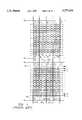
- FIG. 5shows the layout of the buried layer in the select gate enhanced high density ROM device of this invention.
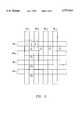
- FIG. 6shows layout of the select gate enhanced high density ROM device of this invention.
- FIG. 7shows the effective circuit of the select gate enhanced high density ROM device of this invention.
- FIG. 8shows the reading path of the select gate enhanced highdensity ROM device of this invention.
- FIG. 9shows another reading path of the select gate enhanced high density ROM device of this invention.
- FIG. 10shows yet another reading path of the select gate enhanced high density ROM device of this invention.
- T0 in the figureis one memory cell which is formed by the cross area of the polysilicon word line WL1 and buried N+ bit line BL1 and BL2.
- the drain and source electrodes of the memory cell T0are the overlapping area I and II of polysilicon word line WL1 and buried N+ line BL1 and BL2.
- the overlapping region of the word line and bit lineis insulated by oxide layer, and the gate electrode of the memory cell T0 is located on the polysilicon word line WL1.
- one horizontal polysilicon word line and two vertical buried N+ bit linecan form the memory cell T1, T2, T01, T02 . . .
- the ROM cell matrix of this inventionis formed by this cross structure of a parallel set of horizontal polysilicon word line and a parallel set of vertical buried N+ bit line.
- FIG. 6shows the layout of the select gate enhanced high density ROM device of this invention.
- a set of select line S1, S2, S3, S4which is perpendicular to the bit line BL1, BL2 . . . is positioned on top and bottom of the ROM matrix respectively. These select lines are used to pick out the areas of ROM devices and facilitate the high density extension of ROM devices.
- metal lines SB1, VG1, SB2, VG2are deposited to lessen the resistance load of the buried N+ bit line.
- the whole ROM matrixis covered with a layer of thin oxide (50) with extended regions.
- select gate SM1, SM2, SM3, SM4Each buried layer N+ BL1, BL2, BL3 . . . has only one extended region to up side or down side. Since the extension of the thin oxide layer can be twice as wide as the buried N+ line, the select gate SM1, SM2, can be twice as large as the memory cell T0, T1, T2, . . . and its driving ability is enhanced by a factor of two. Besides the metal contact area 12, 14, 16, 18 can be formed in SB1, VG1, SB2, VG2 then connect by metal lines directly. And buried line N+ 20, 22, 24, 24 are employed to select the desired select gates.
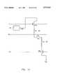
- FIG. 7shows the effective circuit of the select gate high density ROM device disclosed in the invention.
- SB1 and SB2are bit lines.
- VG1 and VG2are virtual ground lines and WL1, WL2,. . . , WLn are word lines.
- S1, S2, S3 and S4provide select lines. Every bit line can transmit 4 different sets data stored in the memory cell and it is described as following:
- the enchanced select gateis achived by employing a thin oxide layer entended region.
- the select gate SM1, SM2,SM3 and SM4, as shown in FIG. 6,can be twice as large as the memory cell and its driving ability is enhanced by a factor of two.
- N+ buried lineis employed to choose the undesired select gate.
- the organization of ROM cell matrixcan be more flexible according to the different buried line structure.
Landscapes
- Read Only Memory (AREA)
Abstract
Description
Claims (5)
Priority Applications (1)
| Application Number | Priority Date | Filing Date | Title |
|---|---|---|---|
| US08/713,741US5777919A (en) | 1996-09-13 | 1996-09-13 | Select gate enhanced high density read-only-memory device |
Applications Claiming Priority (1)
| Application Number | Priority Date | Filing Date | Title |
|---|---|---|---|
| US08/713,741US5777919A (en) | 1996-09-13 | 1996-09-13 | Select gate enhanced high density read-only-memory device |
Publications (1)
| Publication Number | Publication Date |
|---|---|
| US5777919Atrue US5777919A (en) | 1998-07-07 |
Family
ID=24867337
Family Applications (1)
| Application Number | Title | Priority Date | Filing Date |
|---|---|---|---|
| US08/713,741Expired - Fee RelatedUS5777919A (en) | 1996-09-13 | 1996-09-13 | Select gate enhanced high density read-only-memory device |
Country Status (1)
| Country | Link |
|---|---|
| US (1) | US5777919A (en) |
Cited By (44)
| Publication number | Priority date | Publication date | Assignee | Title |
|---|---|---|---|---|
| US5963465A (en)* | 1997-12-12 | 1999-10-05 | Saifun Semiconductors, Ltd. | Symmetric segmented memory array architecture |
| US6430077B1 (en) | 1997-12-12 | 2002-08-06 | Saifun Semiconductors Ltd. | Method for regulating read voltage level at the drain of a cell in a symmetric array |
| US20030072192A1 (en)* | 2000-05-04 | 2003-04-17 | Ilan Bloom | Programming of nonvolatile memory cells |
| US6584017B2 (en) | 2001-04-05 | 2003-06-24 | Saifun Semiconductors Ltd. | Method for programming a reference cell |
| US20030117861A1 (en)* | 2001-12-20 | 2003-06-26 | Eduardo Maayan | NROM NOR array |
| US20030142544A1 (en)* | 2002-01-31 | 2003-07-31 | Eduardo Maayan | Mass storage array and methods for operation thereof |
| US6614692B2 (en) | 2001-01-18 | 2003-09-02 | Saifun Semiconductors Ltd. | EEPROM array and method for operation thereof |
| US6633499B1 (en) | 1997-12-12 | 2003-10-14 | Saifun Semiconductors Ltd. | Method for reducing voltage drops in symmetric array architectures |
| US6633496B2 (en) | 1997-12-12 | 2003-10-14 | Saifun Semiconductors Ltd. | Symmetric architecture for memory cells having widely spread metal bit lines |
| US6636440B2 (en) | 2001-04-25 | 2003-10-21 | Saifun Semiconductors Ltd. | Method for operation of an EEPROM array, including refresh thereof |
| US20030201477A1 (en)* | 1997-07-30 | 2003-10-30 | Boaz Eitan | Non-volatile electrically erasable and programmable semiconductor memory cell utilizing asymmetrical charge trapping |
| US6643181B2 (en) | 2001-10-24 | 2003-11-04 | Saifun Semiconductors Ltd. | Method for erasing a memory cell |
| US6677805B2 (en) | 2001-04-05 | 2004-01-13 | Saifun Semiconductors Ltd. | Charge pump stage with body effect minimization |
| US20040008541A1 (en)* | 2002-07-10 | 2004-01-15 | Eduardo Maayan | Multiple use memory chip |
| US20040022113A1 (en)* | 2002-08-01 | 2004-02-05 | Ran Dvir | High voltage insertion in flash memory cards |
| US6747896B2 (en) | 2002-05-06 | 2004-06-08 | Multi Level Memory Technology | Bi-directional floating gate nonvolatile memory |
| US20050111257A1 (en)* | 1997-08-01 | 2005-05-26 | Boaz Eitan | Two bit non-volatile electrically erasable and programmable semiconductor memory cell utilizing asymmetrical charge trapping |
| US6914820B1 (en) | 2002-05-06 | 2005-07-05 | Multi Level Memory Technology | Erasing storage nodes in a bi-directional nonvolatile memory cell |
| US6928001B2 (en) | 2000-12-07 | 2005-08-09 | Saifun Semiconductors Ltd. | Programming and erasing methods for a non-volatile memory cell |
| US20060036803A1 (en)* | 2004-08-16 | 2006-02-16 | Mori Edan | Non-volatile memory device controlled by a micro-controller |
| US20070103985A1 (en)* | 2002-05-06 | 2007-05-10 | Sau Ching Wong | Fabricating bi-directional nonvolatile memory cells |
| US7221138B2 (en) | 2005-09-27 | 2007-05-22 | Saifun Semiconductors Ltd | Method and apparatus for measuring charge pump output current |
| US7317633B2 (en) | 2004-07-06 | 2008-01-08 | Saifun Semiconductors Ltd | Protection of NROM devices from charge damage |
| US7352627B2 (en) | 2006-01-03 | 2008-04-01 | Saifon Semiconductors Ltd. | Method, system, and circuit for operating a non-volatile memory array |
| US7369440B2 (en) | 2005-01-19 | 2008-05-06 | Saifun Semiconductors Ltd. | Method, circuit and systems for erasing one or more non-volatile memory cells |
| US7420848B2 (en) | 2002-01-31 | 2008-09-02 | Saifun Semiconductors Ltd. | Method, system, and circuit for operating a non-volatile memory array |
| US7457183B2 (en) | 2003-09-16 | 2008-11-25 | Saifun Semiconductors Ltd. | Operating array cells with matched reference cells |
| US7466594B2 (en) | 2004-08-12 | 2008-12-16 | Saifun Semiconductors Ltd. | Dynamic matching of signal path and reference path for sensing |
| US7532529B2 (en) | 2004-03-29 | 2009-05-12 | Saifun Semiconductors Ltd. | Apparatus and methods for multi-level sensing in a memory array |
| US7535765B2 (en) | 2004-12-09 | 2009-05-19 | Saifun Semiconductors Ltd. | Non-volatile memory device and method for reading cells |
| US7590001B2 (en) | 2007-12-18 | 2009-09-15 | Saifun Semiconductors Ltd. | Flash memory with optimized write sector spares |
| US7605579B2 (en) | 2006-09-18 | 2009-10-20 | Saifun Semiconductors Ltd. | Measuring and controlling current consumption and output current of charge pumps |
| US7638850B2 (en) | 2004-10-14 | 2009-12-29 | Saifun Semiconductors Ltd. | Non-volatile memory structure and method of fabrication |
| US7638835B2 (en) | 2006-02-28 | 2009-12-29 | Saifun Semiconductors Ltd. | Double density NROM with nitride strips (DDNS) |
| US7668017B2 (en) | 2005-08-17 | 2010-02-23 | Saifun Semiconductors Ltd. | Method of erasing non-volatile memory cells |
| US7675782B2 (en) | 2002-10-29 | 2010-03-09 | Saifun Semiconductors Ltd. | Method, system and circuit for programming a non-volatile memory array |
| US7692961B2 (en) | 2006-02-21 | 2010-04-06 | Saifun Semiconductors Ltd. | Method, circuit and device for disturb-control of programming nonvolatile memory cells by hot-hole injection (HHI) and by channel hot-electron (CHE) injection |
| US7701779B2 (en) | 2006-04-27 | 2010-04-20 | Sajfun Semiconductors Ltd. | Method for programming a reference cell |
| US7743230B2 (en) | 2003-01-31 | 2010-06-22 | Saifun Semiconductors Ltd. | Memory array programming circuit and a method for using the circuit |
| US7760554B2 (en) | 2006-02-21 | 2010-07-20 | Saifun Semiconductors Ltd. | NROM non-volatile memory and mode of operation |
| US7786512B2 (en) | 2005-07-18 | 2010-08-31 | Saifun Semiconductors Ltd. | Dense non-volatile memory array and method of fabrication |
| US7808818B2 (en) | 2006-01-12 | 2010-10-05 | Saifun Semiconductors Ltd. | Secondary injection for NROM |
| US8053812B2 (en) | 2005-03-17 | 2011-11-08 | Spansion Israel Ltd | Contact in planar NROM technology |
| US8253452B2 (en) | 2006-02-21 | 2012-08-28 | Spansion Israel Ltd | Circuit and method for powering up an integrated circuit and an integrated circuit utilizing same |
Citations (1)
| Publication number | Priority date | Publication date | Assignee | Title |
|---|---|---|---|---|
| US5268861A (en)* | 1991-04-10 | 1993-12-07 | Sharp Kabushiki Kaisha | Semiconductor read only memory |
- 1996
- 1996-09-13USUS08/713,741patent/US5777919A/ennot_activeExpired - Fee Related
Patent Citations (1)
| Publication number | Priority date | Publication date | Assignee | Title |
|---|---|---|---|---|
| US5268861A (en)* | 1991-04-10 | 1993-12-07 | Sharp Kabushiki Kaisha | Semiconductor read only memory |
Cited By (66)
| Publication number | Priority date | Publication date | Assignee | Title |
|---|---|---|---|---|
| US6803299B2 (en) | 1997-07-30 | 2004-10-12 | Saifun Semiconductors Ltd. | Non-volatile electrically erasable and programmable semiconductor memory cell utilizing asymmetrical charge trapping |
| US20030201477A1 (en)* | 1997-07-30 | 2003-10-30 | Boaz Eitan | Non-volatile electrically erasable and programmable semiconductor memory cell utilizing asymmetrical charge trapping |
| US7405969B2 (en) | 1997-08-01 | 2008-07-29 | Saifun Semiconductors Ltd. | Non-volatile memory cell and non-volatile memory devices |
| US7116577B2 (en) | 1997-08-01 | 2006-10-03 | Saifun Semiconductors Ltd | Two bit non-volatile electrically erasable and programmable semiconductor memory cell utilizing asymmetrical charge trapping |
| US20050111257A1 (en)* | 1997-08-01 | 2005-05-26 | Boaz Eitan | Two bit non-volatile electrically erasable and programmable semiconductor memory cell utilizing asymmetrical charge trapping |
| US6285574B1 (en)* | 1997-12-12 | 2001-09-04 | Saifun Semiconductors Ltd. | Symmetric segmented memory array architecture |
| US6335874B1 (en)* | 1997-12-12 | 2002-01-01 | Saifun Semiconductors Ltd. | Symmetric segmented memory array architecture |
| US6430077B1 (en) | 1997-12-12 | 2002-08-06 | Saifun Semiconductors Ltd. | Method for regulating read voltage level at the drain of a cell in a symmetric array |
| US5963465A (en)* | 1997-12-12 | 1999-10-05 | Saifun Semiconductors, Ltd. | Symmetric segmented memory array architecture |
| US6633499B1 (en) | 1997-12-12 | 2003-10-14 | Saifun Semiconductors Ltd. | Method for reducing voltage drops in symmetric array architectures |
| US6633496B2 (en) | 1997-12-12 | 2003-10-14 | Saifun Semiconductors Ltd. | Symmetric architecture for memory cells having widely spread metal bit lines |
| US20030072192A1 (en)* | 2000-05-04 | 2003-04-17 | Ilan Bloom | Programming of nonvolatile memory cells |
| US6829172B2 (en) | 2000-05-04 | 2004-12-07 | Saifun Semiconductors Ltd. | Programming of nonvolatile memory cells |
| US6937521B2 (en) | 2000-05-04 | 2005-08-30 | Saifun Semiconductors Ltd. | Programming and erasing methods for a non-volatile memory cell |
| US6928001B2 (en) | 2000-12-07 | 2005-08-09 | Saifun Semiconductors Ltd. | Programming and erasing methods for a non-volatile memory cell |
| US6614692B2 (en) | 2001-01-18 | 2003-09-02 | Saifun Semiconductors Ltd. | EEPROM array and method for operation thereof |
| US7518908B2 (en) | 2001-01-18 | 2009-04-14 | Saifun Semiconductors Ltd. | EEPROM array and method for operation thereof |
| US20040130385A1 (en)* | 2001-04-05 | 2004-07-08 | Shor Joseph S. | Charge pump stage with body effect minimization |
| US6864739B2 (en) | 2001-04-05 | 2005-03-08 | Saifun Semiconductors Ltd. | Charge pump stage with body effect minimization |
| US6584017B2 (en) | 2001-04-05 | 2003-06-24 | Saifun Semiconductors Ltd. | Method for programming a reference cell |
| US7064983B2 (en) | 2001-04-05 | 2006-06-20 | Saifum Semiconductors Ltd. | Method for programming a reference cell |
| US6677805B2 (en) | 2001-04-05 | 2004-01-13 | Saifun Semiconductors Ltd. | Charge pump stage with body effect minimization |
| US6636440B2 (en) | 2001-04-25 | 2003-10-21 | Saifun Semiconductors Ltd. | Method for operation of an EEPROM array, including refresh thereof |
| US6643181B2 (en) | 2001-10-24 | 2003-11-04 | Saifun Semiconductors Ltd. | Method for erasing a memory cell |
| US6888757B2 (en) | 2001-10-24 | 2005-05-03 | Saifun Semiconductors Ltd. | Method for erasing a memory cell |
| US6885585B2 (en) | 2001-12-20 | 2005-04-26 | Saifun Semiconductors Ltd. | NROM NOR array |
| US20030117861A1 (en)* | 2001-12-20 | 2003-06-26 | Eduardo Maayan | NROM NOR array |
| US20030142544A1 (en)* | 2002-01-31 | 2003-07-31 | Eduardo Maayan | Mass storage array and methods for operation thereof |
| US6975536B2 (en) | 2002-01-31 | 2005-12-13 | Saifun Semiconductors Ltd. | Mass storage array and methods for operation thereof |
| US7420848B2 (en) | 2002-01-31 | 2008-09-02 | Saifun Semiconductors Ltd. | Method, system, and circuit for operating a non-volatile memory array |
| US7221591B1 (en) | 2002-05-06 | 2007-05-22 | Samsung Electronics Co., Ltd. | Fabricating bi-directional nonvolatile memory cells |
| US6914820B1 (en) | 2002-05-06 | 2005-07-05 | Multi Level Memory Technology | Erasing storage nodes in a bi-directional nonvolatile memory cell |
| US6826084B1 (en) | 2002-05-06 | 2004-11-30 | Multi Level Memory Technology | Accessing individual storage nodes in a bi-directional nonvolatile memory cell |
| US7355891B2 (en) | 2002-05-06 | 2008-04-08 | Samsung Electronics Co., Ltd. | Fabricating bi-directional nonvolatile memory cells |
| US6747896B2 (en) | 2002-05-06 | 2004-06-08 | Multi Level Memory Technology | Bi-directional floating gate nonvolatile memory |
| US20070103985A1 (en)* | 2002-05-06 | 2007-05-10 | Sau Ching Wong | Fabricating bi-directional nonvolatile memory cells |
| US20040008541A1 (en)* | 2002-07-10 | 2004-01-15 | Eduardo Maayan | Multiple use memory chip |
| US7738304B2 (en) | 2002-07-10 | 2010-06-15 | Saifun Semiconductors Ltd. | Multiple use memory chip |
| US6917544B2 (en) | 2002-07-10 | 2005-07-12 | Saifun Semiconductors Ltd. | Multiple use memory chip |
| US6826107B2 (en) | 2002-08-01 | 2004-11-30 | Saifun Semiconductors Ltd. | High voltage insertion in flash memory cards |
| US20040022113A1 (en)* | 2002-08-01 | 2004-02-05 | Ran Dvir | High voltage insertion in flash memory cards |
| US7675782B2 (en) | 2002-10-29 | 2010-03-09 | Saifun Semiconductors Ltd. | Method, system and circuit for programming a non-volatile memory array |
| US7743230B2 (en) | 2003-01-31 | 2010-06-22 | Saifun Semiconductors Ltd. | Memory array programming circuit and a method for using the circuit |
| US7457183B2 (en) | 2003-09-16 | 2008-11-25 | Saifun Semiconductors Ltd. | Operating array cells with matched reference cells |
| US7532529B2 (en) | 2004-03-29 | 2009-05-12 | Saifun Semiconductors Ltd. | Apparatus and methods for multi-level sensing in a memory array |
| US7317633B2 (en) | 2004-07-06 | 2008-01-08 | Saifun Semiconductors Ltd | Protection of NROM devices from charge damage |
| US7466594B2 (en) | 2004-08-12 | 2008-12-16 | Saifun Semiconductors Ltd. | Dynamic matching of signal path and reference path for sensing |
| US20060036803A1 (en)* | 2004-08-16 | 2006-02-16 | Mori Edan | Non-volatile memory device controlled by a micro-controller |
| US7638850B2 (en) | 2004-10-14 | 2009-12-29 | Saifun Semiconductors Ltd. | Non-volatile memory structure and method of fabrication |
| US7964459B2 (en) | 2004-10-14 | 2011-06-21 | Spansion Israel Ltd. | Non-volatile memory structure and method of fabrication |
| US7535765B2 (en) | 2004-12-09 | 2009-05-19 | Saifun Semiconductors Ltd. | Non-volatile memory device and method for reading cells |
| US7369440B2 (en) | 2005-01-19 | 2008-05-06 | Saifun Semiconductors Ltd. | Method, circuit and systems for erasing one or more non-volatile memory cells |
| US7468926B2 (en) | 2005-01-19 | 2008-12-23 | Saifun Semiconductors Ltd. | Partial erase verify |
| US8053812B2 (en) | 2005-03-17 | 2011-11-08 | Spansion Israel Ltd | Contact in planar NROM technology |
| US7786512B2 (en) | 2005-07-18 | 2010-08-31 | Saifun Semiconductors Ltd. | Dense non-volatile memory array and method of fabrication |
| US7668017B2 (en) | 2005-08-17 | 2010-02-23 | Saifun Semiconductors Ltd. | Method of erasing non-volatile memory cells |
| US7221138B2 (en) | 2005-09-27 | 2007-05-22 | Saifun Semiconductors Ltd | Method and apparatus for measuring charge pump output current |
| US7352627B2 (en) | 2006-01-03 | 2008-04-01 | Saifon Semiconductors Ltd. | Method, system, and circuit for operating a non-volatile memory array |
| US7808818B2 (en) | 2006-01-12 | 2010-10-05 | Saifun Semiconductors Ltd. | Secondary injection for NROM |
| US7760554B2 (en) | 2006-02-21 | 2010-07-20 | Saifun Semiconductors Ltd. | NROM non-volatile memory and mode of operation |
| US7692961B2 (en) | 2006-02-21 | 2010-04-06 | Saifun Semiconductors Ltd. | Method, circuit and device for disturb-control of programming nonvolatile memory cells by hot-hole injection (HHI) and by channel hot-electron (CHE) injection |
| US8253452B2 (en) | 2006-02-21 | 2012-08-28 | Spansion Israel Ltd | Circuit and method for powering up an integrated circuit and an integrated circuit utilizing same |
| US7638835B2 (en) | 2006-02-28 | 2009-12-29 | Saifun Semiconductors Ltd. | Double density NROM with nitride strips (DDNS) |
| US7701779B2 (en) | 2006-04-27 | 2010-04-20 | Sajfun Semiconductors Ltd. | Method for programming a reference cell |
| US7605579B2 (en) | 2006-09-18 | 2009-10-20 | Saifun Semiconductors Ltd. | Measuring and controlling current consumption and output current of charge pumps |
| US7590001B2 (en) | 2007-12-18 | 2009-09-15 | Saifun Semiconductors Ltd. | Flash memory with optimized write sector spares |
Similar Documents
| Publication | Publication Date | Title |
|---|---|---|
| US5777919A (en) | Select gate enhanced high density read-only-memory device | |
| KR100423896B1 (en) | A scalable two transistor memory device | |
| US5257224A (en) | Semiconductor device with multiple layers of memory cell arrays | |
| US8674459B2 (en) | Three-dimensional memory devices and methods of manufacturing and operating the same | |
| US6084794A (en) | High speed flat-cell mask ROM structure with select lines | |
| US6872999B2 (en) | Semiconductor storage device with signal wiring lines RMED above memory cells | |
| US5825683A (en) | Folded read-only memory | |
| US6583490B2 (en) | One time programmable semiconductor nonvolatile memory device and method for production of same | |
| JPH04257260A (en) | Read-only memory integrated circuit | |
| US7215563B2 (en) | Multi-layered memory cell structure | |
| US6879511B2 (en) | Memory on a SOI substrate | |
| KR20030040122A (en) | Semiconductor memory device | |
| CN100468739C (en) | Semiconductor device with layered bit lines | |
| CN109390005A (en) | Semiconductor storage unit | |
| US5621697A (en) | High density integrated circuit with bank select structure | |
| KR100545971B1 (en) | Nonvolatile semiconductor memory | |
| KR100275193B1 (en) | Semiconductor memory device | |
| US7327593B2 (en) | ROM memory cell having defined bit line voltages | |
| JP2000101050A (en) | Semiconductor memory device and layout method of memory cell | |
| US20050111250A1 (en) | High density memory array | |
| US6646312B1 (en) | Semiconductor memory device with bit lines having reduced cross-talk | |
| KR101037501B1 (en) | Highly integrated semiconductor memory | |
| US6642587B1 (en) | High density ROM architecture | |
| JP2006080253A (en) | Semiconductor memory device | |
| US5612915A (en) | Clamp circuit for read-only-memory devices |
Legal Events
| Date | Code | Title | Description |
|---|---|---|---|
| AS | Assignment | Owner name:HOLTEK MICROELECTRONICS, INC., TAIWAN Free format text:ASSIGNMENT OF ASSIGNORS INTEREST;ASSIGNORS:CHI-YUNG, WU;CHEN, LING;PENG, TONY;REEL/FRAME:008221/0265;SIGNING DATES FROM 19960823 TO 19960826 | |
| AS | Assignment | Owner name:UTEK SEMICONDUCTOR CORP., TAIWAN Free format text:CHANGE OF NAME;ASSIGNOR:HOLTEK MICROELECTRONICS, INC.;REEL/FRAME:009490/0001 Effective date:19980630 | |
| AS | Assignment | Owner name:UNITED MICROELECTRONICS CORP., TAIWAN Free format text:ASSIGNMENT OF ASSIGNORS INTEREST;ASSIGNOR:UTEK SEMICONDUCTOR CORP.;REEL/FRAME:010568/0175 Effective date:19991221 | |
| FEPP | Fee payment procedure | Free format text:PAYOR NUMBER ASSIGNED (ORIGINAL EVENT CODE: ASPN); ENTITY STATUS OF PATENT OWNER: LARGE ENTITY | |
| FPAY | Fee payment | Year of fee payment:4 | |
| FPAY | Fee payment | Year of fee payment:8 | |
| REMI | Maintenance fee reminder mailed | ||
| LAPS | Lapse for failure to pay maintenance fees | ||
| STCH | Information on status: patent discontinuation | Free format text:PATENT EXPIRED DUE TO NONPAYMENT OF MAINTENANCE FEES UNDER 37 CFR 1.362 | |
| FP | Lapsed due to failure to pay maintenance fee | Effective date:20100707 |