US5777596A - Touch sensitive flat panel display - Google Patents
Touch sensitive flat panel displayDownload PDFInfo
- Publication number
- US5777596A US5777596AUS08/556,689US55668995AUS5777596AUS 5777596 AUS5777596 AUS 5777596AUS 55668995 AUS55668995 AUS 55668995AUS 5777596 AUS5777596 AUS 5777596A
- Authority
- US
- United States
- Prior art keywords
- elements
- lcd
- display
- charge
- voltage
- Prior art date
- Legal status (The legal status is an assumption and is not a legal conclusion. Google has not performed a legal analysis and makes no representation as to the accuracy of the status listed.)
- Expired - Lifetime
Links
Images


Classifications
- G—PHYSICS
- G06—COMPUTING OR CALCULATING; COUNTING
- G06F—ELECTRIC DIGITAL DATA PROCESSING
- G06F3/00—Input arrangements for transferring data to be processed into a form capable of being handled by the computer; Output arrangements for transferring data from processing unit to output unit, e.g. interface arrangements
- G06F3/01—Input arrangements or combined input and output arrangements for interaction between user and computer
- G06F3/03—Arrangements for converting the position or the displacement of a member into a coded form
- G06F3/041—Digitisers, e.g. for touch screens or touch pads, characterised by the transducing means
- G06F3/0412—Digitisers structurally integrated in a display
- G—PHYSICS
- G06—COMPUTING OR CALCULATING; COUNTING
- G06F—ELECTRIC DIGITAL DATA PROCESSING
- G06F3/00—Input arrangements for transferring data to be processed into a form capable of being handled by the computer; Output arrangements for transferring data from processing unit to output unit, e.g. interface arrangements
- G06F3/01—Input arrangements or combined input and output arrangements for interaction between user and computer
- G06F3/03—Arrangements for converting the position or the displacement of a member into a coded form
- G06F3/041—Digitisers, e.g. for touch screens or touch pads, characterised by the transducing means
- G06F3/0416—Control or interface arrangements specially adapted for digitisers
- G06F3/04166—Details of scanning methods, e.g. sampling time, grouping of sub areas or time sharing with display driving
- G—PHYSICS
- G06—COMPUTING OR CALCULATING; COUNTING
- G06F—ELECTRIC DIGITAL DATA PROCESSING
- G06F3/00—Input arrangements for transferring data to be processed into a form capable of being handled by the computer; Output arrangements for transferring data from processing unit to output unit, e.g. interface arrangements
- G06F3/01—Input arrangements or combined input and output arrangements for interaction between user and computer
- G06F3/03—Arrangements for converting the position or the displacement of a member into a coded form
- G06F3/041—Digitisers, e.g. for touch screens or touch pads, characterised by the transducing means
- G06F3/044—Digitisers, e.g. for touch screens or touch pads, characterised by the transducing means by capacitive means
- G—PHYSICS
- G06—COMPUTING OR CALCULATING; COUNTING
- G06F—ELECTRIC DIGITAL DATA PROCESSING
- G06F3/00—Input arrangements for transferring data to be processed into a form capable of being handled by the computer; Output arrangements for transferring data from processing unit to output unit, e.g. interface arrangements
- G06F3/01—Input arrangements or combined input and output arrangements for interaction between user and computer
- G06F3/048—Interaction techniques based on graphical user interfaces [GUI]
- G06F3/0481—Interaction techniques based on graphical user interfaces [GUI] based on specific properties of the displayed interaction object or a metaphor-based environment, e.g. interaction with desktop elements like windows or icons, or assisted by a cursor's changing behaviour or appearance
- G06F3/04812—Interaction techniques based on cursor appearance or behaviour, e.g. being affected by the presence of displayed objects
- G—PHYSICS
- G09—EDUCATION; CRYPTOGRAPHY; DISPLAY; ADVERTISING; SEALS
- G09G—ARRANGEMENTS OR CIRCUITS FOR CONTROL OF INDICATING DEVICES USING STATIC MEANS TO PRESENT VARIABLE INFORMATION
- G09G3/00—Control arrangements or circuits, of interest only in connection with visual indicators other than cathode-ray tubes
- G09G3/20—Control arrangements or circuits, of interest only in connection with visual indicators other than cathode-ray tubes for presentation of an assembly of a number of characters, e.g. a page, by composing the assembly by combination of individual elements arranged in a matrix no fixed position being assigned to or needed to be assigned to the individual characters or partial characters
- G09G3/34—Control arrangements or circuits, of interest only in connection with visual indicators other than cathode-ray tubes for presentation of an assembly of a number of characters, e.g. a page, by composing the assembly by combination of individual elements arranged in a matrix no fixed position being assigned to or needed to be assigned to the individual characters or partial characters by control of light from an independent source
- G09G3/36—Control arrangements or circuits, of interest only in connection with visual indicators other than cathode-ray tubes for presentation of an assembly of a number of characters, e.g. a page, by composing the assembly by combination of individual elements arranged in a matrix no fixed position being assigned to or needed to be assigned to the individual characters or partial characters by control of light from an independent source using liquid crystals
- G09G3/3611—Control of matrices with row and column drivers
- G09G3/3648—Control of matrices with row and column drivers using an active matrix
- G—PHYSICS
- G02—OPTICS
- G02F—OPTICAL DEVICES OR ARRANGEMENTS FOR THE CONTROL OF LIGHT BY MODIFICATION OF THE OPTICAL PROPERTIES OF THE MEDIA OF THE ELEMENTS INVOLVED THEREIN; NON-LINEAR OPTICS; FREQUENCY-CHANGING OF LIGHT; OPTICAL LOGIC ELEMENTS; OPTICAL ANALOGUE/DIGITAL CONVERTERS
- G02F1/00—Devices or arrangements for the control of the intensity, colour, phase, polarisation or direction of light arriving from an independent light source, e.g. switching, gating or modulating; Non-linear optics
- G02F1/01—Devices or arrangements for the control of the intensity, colour, phase, polarisation or direction of light arriving from an independent light source, e.g. switching, gating or modulating; Non-linear optics for the control of the intensity, phase, polarisation or colour
- G02F1/13—Devices or arrangements for the control of the intensity, colour, phase, polarisation or direction of light arriving from an independent light source, e.g. switching, gating or modulating; Non-linear optics for the control of the intensity, phase, polarisation or colour based on liquid crystals, e.g. single liquid crystal display cells
- G02F1/133—Constructional arrangements; Operation of liquid crystal cells; Circuit arrangements
- G02F1/1333—Constructional arrangements; Manufacturing methods
- G02F1/13338—Input devices, e.g. touch panels
Definitions
- the inventionrelates in general to liquid crystal flat panel displays and, more particularly, to displays which are responsive to the touch of a user.
- LCDLiquid Crystal Display
- a stylusis a pointing device which a computer operator can use to indicate a specific location on a display device to a host computer while performing computer applications.
- a styluscan be used as a replacement for other types of pointing devices, such as mice and track balls.
- a styluscan be used in a process known as inking, wherein a user runs the tip of the stylus across the display surface of a display device, such as an LCD, while a host computer simultaneously illuminates the pixels on the display device traversed by the stylus tip.
- inkingwherein a user runs the tip of the stylus across the display surface of a display device, such as an LCD, while a host computer simultaneously illuminates the pixels on the display device traversed by the stylus tip.
- a computer system using a stylushas to have some way of sensing the position of the stylus tip on the screen of the display device.
- a number of approacheshave been used in the past to accomplish this.
- a resistive or capacitive sensing membraneis placed over the display screen to sense the location of the stylus.
- the styluscommunicates its position to a host computer by transmitting an RF signal to receiver circuitry attached to the display screen.
- the stylustransmits position information to a host computer via an electrical cable.
- the disadvantage of known past approachesis that they either require a special stylus, which may be costly and can be misplaced, or they require special sensing devices attached to the display, which adds to the cost and weight of the product. It would be desirable to have a system in which a common object, such as a ball point pen or an operator's finger, could be used as a pointing device without the need for bulky sensing devices attached to the display.
- the present inventionfulfills the above-mentioned need by providing a touch sensitive LCD flat panel display which takes advantage of the unique properties of liquid crystal display elements to allow a user to provide input into a computer device by simply touching an LCD display screen with a passive device, such as a finger, stylus or a ball point pen.
- a passive devicesuch as a finger, stylus or a ball point pen.
- the inventionprovides all of the pointing capabilities of past stylus designs without the need for a special pen or bulky sensing circuitry.
- one aspect of the present inventionincludes: (a) a plurality of LCD elements, (b) means for applying a charge to each of the elements, c means for monitoring a voltage across each of the elements and for using the voltage to compare the charge time of each of the elements to a reference charge time value; and (d) means, responsive to the means for monitoring, for determining which, if any, of the LCD elements in the plurality are being touched.
- the inventiondoes the charge time comparison by applying a charge to all of the elements in a row and determining which of the elements have charged up to a predetermined voltage by the time a strobe line is pulsed.
- the strobeis pulsed multiple times during a charging cycle resulting in weighted charge time information.
- a counteris used to time the period for which an element has exceeded a reference voltage as an indication of the charge time of the element.
- another aspect of the present inventionincludes: (a) an LCD element including: (I) a front transparent plate having a first surface and a second surface, the first surface having a front electrode disposed adjacent thereto; (ii) a rear transparent plate positioned substantially parallel to, and in fixed relation to, the front transparent plate, the rear transparent plate having a rear electrode disposed adjacent to a second surface thereof, the first surface of the rear transparent plate facing the first surface of the front transparent plate so that the front electrode is substantially opposite the rear electrode; and (iii) a layer of liquid crystal material between the first surface of the front transparent plate and the first surface of the rear transparent plate, the layer capable of changing optical properties when a predetermined voltage is applied across the front and rear electrodes; (iv) wherein the LCD element has a capacitance between the front and rear electrodes which changes when a user touches the second surface of the front transparent plate; (b) means for determining whether the surface of the front transparent plate is being touched by a user based on the change in capacitance; and (c
- the means for increasingincludes a means for diffusing a conductive material into the front transparent plate adjacent to the front electrode.
- the means for increasingincludes a means for embedding the front electrode into the front transparent plate.
- a resistive materialis diffused in the transparent plate, allowing limited current flow between the electrode of the display element and an external stylus or finger.
- an imagebe displayed on an LCD at substantially the same time that touches to the LCD screen are being monitored. Because the display of an image requires that a predetermined voltage be maintained on the elements of the display (including typically zero volts for black or non-illuminated pixels), it is impossible to constantly charge and discharge every element in the display to sense touches to the screen.
- a third aspect of the present inventionincludes: (a) means for alternately charging and discharging the display elements in a subgroup of the display elements in a display screen; (b) means for comparing a charge time of each of the display elements in the subgroup to a reference charge time value; and (c) means for processing the results of the comparison to determine which, if any, of the display elements in the subgroup are being touched; wherein the display elements in the display screen which are not in the subgroup continuously display an image on the display screen.
- the subgroup of display elementsproduce a blinking cursor on the display screen.
- the subgroup of display elementscomprises a row of display elements on the display screen. This row may be periodically changed so that every row of the display screen is periodically scanned.
- FIG. 1is a sectional view of a typical LCD element
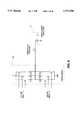
- FIG. 2is a schematic diagram illustrating a portion of a typical active matrix liquid crystal display
- FIG. 4illustrates one embodiment of the display system of the present invention
- FIG. 5illustrates one embodiment of the display driver circuitry of FIG. 4
- FIG. 6illustrates one embodiment of the charge control unit of FIG. 5
- FIG. 7illustrates another embodiment of the display driver circuitry of FIG. 4
- FIG. 8is a charge time plot illustrating the relative charge times of the display elements in an LCD display, which can be created using one embodiment of the present invention
- FIG. 9is a weighted charge time plot illustrating the relative charge times of the display elements in an LCD display, which can be created using another embodiment of the present invention.
- FIG. 10illustrates another embodiment of the display driver circuitry of FIG. 4
- FIG. 11illustrates yet another embodiment of the display driver circuitry of FIG. 4.
- FIG. 12illustrates a charge control unit for use in another embodiment of the present invention.
- the present inventionrelates to a touch sensitive LCD flat panel display.
- the displayallows a user to provide input into a computer device by simply touching an LCD display screen with a passive device, such as a finger, stylus, or a ball point pen.
- the inventionincludes circuitry which continuously compares the charge times of the liquid crystal elements of the display to a reference value and uses the results of the comparison to determine which elements are currently being touched.
- LCDliquid crystal display
- FIG. 1is a sectional view of a typical liquid crystal display element 10.
- the element 10includes: front glass 12, rear glass 14, front electrode 16, rear electrode 18, and liquid crystal layer 20.
- the front and rear glass 12, 14are flat, transparent elements which are used to contain the thin layer of liquid crystal material 20 and to provide a substrate for deposition of the electrodes 16, 18.
- the electrodes 16, 18are operative for supplying the electrical signals to the liquid crystal material to change the optical properties of the material.
- the electrodes 16, 18are normally made of a transparent conductive material which can be easily deposited on the inside surface of the corresponding glass piece 12, 14. Because the liquid crystal display element includes two electrodes separated by a dielectric material, it behaves electrically much like a capacitor. That is, when a voltage is provided across the two electrodes, the element "charges up" to the applied voltage level.
- the liquid crystal material comprising the liquid crystal layer 20is made up of electrically polar molecules 22 which orient themselves according to the electric field emanating from the electrodes. Because the molecules are optically and physically anisotropic, the optical properties of the liquid crystal material, as viewed from a stationary reference point, change as the molecules reorient themselves with the electric field. In general, the potential difference across the thin layer 20 must exceed a specific RMS threshold voltage before any change in optical properties is apparent.
- a multitude of elements 10are arranged in an array pattern which allows a wide variety of display images to be displayed.
- a problemarises in how to address each element in the array in order to create a desired display image.
- two different types of LCD arrays, each using a different type of addressing,have been developed. It should be appreciated that the present invention can be used with either type of LCD array.
- a passive displayIn the first type of array, known as a passive display, all of the front electrodes in each row (or column) are connected to a common row bus and all of the rear electrodes in each column (or row) are connected to a common column bus. (Alternatively, a passive display may divide the array into a number of regions for which all of the front electrodes in each row of each region are connected to a common row bus, etc.) To address a particular display element in the array, a positive voltage is applied to the appropriate row bus and a negative voltage is applied to the appropriate column bus (or vice versa) so that a composite RMS voltage exceeding the threshold voltage is applied across the selected element.
- a second type of LCD arrayis known as an active matrix display.
- An active matrix displayincludes a separate electronically controlled switch 24 at each LCD element 26.
- This switch 24may take the form of a MOS thin film transistor (TFT) deposited adjacent to the corresponding element on the glass substrate.
- TFTMOS thin film transistor
- the switchesmay be turned on and off by applying a voltage to or removing a voltage from a control terminal 28. If a MOS device is being used, for example, the control terminal 28 is the gate terminal of the MOS device.
- all of the switch control terminals 28 associated with a particular row of the arrayare connected to a common row bus, such as Row Line M in FIG. 2.
- a voltageis applied to this row bus, each of the elements in that particular row are connected to a corresponding column bus.
- Voltagesmay then be delivered to each of the elements in the selected row, via the corresponding column busses, to set the desired display state of each of the elements.
- the display voltagesmay be delivered to the display elements one column at a time or, more preferably, all at the same time.
- a separate display control unit(not shown) synchronizes the delivery of display voltages to the display elements to create the desired images.
- the display control unitmay include, for example, a microprocessor or sequencer for controlling the operation and timing of the elements, a display memory for storing display data for the entire array, and a line buffer for storing and transferring voltage select signals for the selected row of the display. Because the voltage level applied to the corresponding column bus of a display element in an active matrix display is not limited like it is for a passive display, a wide range of voltages may be applied to the column bus and variable intensities may be achieved.
- the display elements of a liquid crystal displaybehave like capacitors.
- the charge time of a capacitive circuitis related to the capacitance of the circuit. Therefore, measuring the relative charge time (or discharge time) of the display elements is an indirect method of measuring the relative capacitance of the elements.
- the electrical characteristics of an LCD elementwill change when an object, such as a ball point pen or a person's finger, is brought close to one of the electrodes. This will occur, for example, when a user touches the surface of an LCD display screen.
- an objectsuch as a passive stylus which changes the capacitance of an LCD display element, when brought in contact with the display surface. Because the capacitance of an LCD element changes when touched, the charge time of the element will change accordingly.
- the present inventionperiodically compares the charge (or discharge) time of each element in an LCD array to a reference value and uses the result of the comparison to indicate which of the display elements in the array is currently being touched by the passive stylus. As will be described in more detail, a number of different methods for comparing charge times may be used in accordance with the present invention.
- the thickness of the glassmay result in a condition such that neighboring display elements have a larger contribution to sensed capacitance changes than does the presence of additional capacitance on the other side of the glass or that the capacitance of the interconnecting wires is much greater than that of the display element.
- the thickness of the glassmay be required, however, to provide structural rigidity.
- various glass structuresare provided which accommodate the above-mentioned conditions by effectively reducing the thickness of the glass as sensed by the display elements, while maintaining the required structural rigidity.
- FIG. 3(a)illustrates a typical top panel glass having associated electrodes 16.
- FIG. 3(b)illustrates a similar structure with the addition of an area 17, located above each electrode 16, diffused with a conductive dopant material.
- This diffused area 17effectively moves the segment electrodes 16 close to the surface of the display, making it possible to sense the presence of a passive stylus above the glass 12 with much greater accuracy.
- FIG. 3(d)takes the above approach one step further by having the diffused area 17 extend completely through the glass 12. This approach supports resistive coupling between the electrode 16 and the passive stylus and, therefore, is extremely sensitive to touching.
- FIG. 3(c)illustrates a glass structure having an electrode 19 which is partially embedded in the glass. This structure is similar in effect to the structure of FIG. 3(b), but uses a metalized rather than diffused approach.
- FIG. 4illustrates one embodiment of an LCD system in accordance with the present invention.
- the apparatus of FIG. 4includes a display panel section 30 and a display driver section 32. Both of these sections are controlled by an external display control unit which is not shown in the figure.
- the display panel section 30comprises an active matrix array and, therefore, the following discussion will be with respect to such an array. It should be understood, however, that, as discussed previously, the invention is equally applicable to passive arrays.
- the display driver section 32includes a plurality of column driver units 34, one unit being connected to each column line in the array.
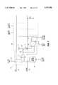
- FIG. 5is a block diagram illustrating one embodiment of the column driver units of FIG. 4. As seen in FIG. 5, each column driver unit 34 may include a charge control unit 36 and a charge time measurement and comparison unit (CMCU) 38.
- CMCUcharge time measurement and comparison unit
- the charge control unit 36is operative for sourcing or sinking current until a specific voltage is attained on a corresponding column line 37 in response to a voltage select signal from a display control unit (not shown). Once on the column line 37, the charge control unit acts upon whichever display element 10 in that column is electrically connected to the column line 37 through the corresponding electronically controlled switch 24 (i.e., the selected display element).
- the display control unit(not shown) controls which display element is connected to the column line 37 by delivering a voltage to the appropriate row line.
- the level of the voltage applied to the selected display element by the charge control unit 36depends upon the display state which the display control unit determines that the element should be displaying. If variable intensities are being used, the applied voltage can take any one of a number of different values.
- FIG. 6illustrates one embodiment of a charge control unit 36 which may be used in the present invention to supply current, reaching one of a number of voltages, to a selected display element 10.
- the unit 36receives Voltage Select A and Voltage Select B signals from the display control unit and delivers a corresponding current and voltage to the display element 10 based on a chosen voltage division of a reference voltage, v.
- the CMCU 38is operative for comparing the charge time of the selected display element to a reference value, Vref, and for creating an output signal indicative of the result of the comparison. It should be understood that many different methods of comparing charge times may be implemented in accordance with the present invention and the embodiment illustrated in FIG. 5 represents only a single way of accomplishing the comparison.
- each CMCU 38includes: a comparator 40, a switch 42, and a data latch 44.
- the comparator 40has a positive input terminal connected to a corresponding column line 37 and a negative input terminal connected to a reference voltage line 48. As illustrated in FIG. 5, a single reference voltage line 48 services all of the CMCUs 38 in the apparatus.
- the output of the comparator 40is connected to a switch control terminal 46 of switch 42 for controlling the electrical connection between a voltage source 47 and a strobe line 50.
- the strobe line 50is connected to the clock terminal of the data latch 44 in every CMCU 38 in the display driver section 32.
- the output of the comparator 40is also connected to the data input of data latch 44.
- Data latch 44has a latched output terminal 52 which may be connected to the display control device (not shown) and a reset input terminal which may receive commands from the display control device.
- the circuitry of FIG. 5operates as follows.
- Charge control unit 36supplies current to column line 37 which begins to charge up the selected display element in the corresponding column.
- the comparator 40monitors the voltage present on the column line 37 and outputs a logic high signal if and when this voltage exceeds the voltage on reference voltage line 48, i.e., Vref. It should be appreciated that the reference voltage, Vref, used in this embodiment, and all other embodiments of the present invention, may be adjustable.
- the logic high signal at the output of comparator 40turns on switch 42 which connects voltage source 47 to the strobe line 50.
- each intersection of a row line and a column linerepresents a single display element 10.
- the dark spots in the arrayrepresent display elements which have relative charge times longer than those of the other elements and thus indicate that the element has a higher capacitance, i.e., the element is probably being touched by a passive stylus.
- the first column line 37 to exceed the reference voltageis the one which causes a voltage to be applied to the strobe line. Because there is little delay between the time when the reference voltage is first exceeded and the time when the data latches 44 are clocked, only a few of the fastest charging display elements will normally reach the reference voltage by the time the data latches 44 are clocked and thus produce a logic one at the latched output terminal 52 of their respective CMCU 38. In general, it is desired that most of the display elements 10 reach the reference voltage by the time of latching so that an indication is made as to which of the data elements 10 in the selected row charge the slowest and thus represent elements which are probably being touched. Therefore, in a variation of the embodiment of FIG. 5, as illustrated in FIG.
- a delay element 53may be inserted between the switch 42 and the strobe line 50.
- This delay element 52delays the application of the voltage to the strobe line 50 after the switch 42 is turned on and, therefore, allows a larger number of column lines 37 to exceed the reference voltage before the data latches 44 are clocked.
- This delaywhich can be made variable, provides a means to compensate for inherent differences in charge time between data elements due to, among other things, manufacturing nonuniformities and also provides a means for tuning the display device based on such things as the type of passive stylus being used.
- the strobe line 50is incapable of clocking the data latches 44 until a predetermined number of CMCUs 38 are driving the line 50. This has substantially the same effect as the delay element 52 described above in that a larger number of column lines are allowed to reach the reference voltage before the data latches are clocked.
- an externally generated strobe signalis input onto strobe line 50 from an external source such as the display control device (not shown).
- the external strobe signalmay be created in a number of different ways.
- the strobe signalis created based on a predetermined delay with respect to the time when the charge control units 36 are enabled. In other words, a logic high signal is applied to the strobe line 50 a predetermined period of time after the charge control units 36 apply voltages to their corresponding column lines 37.
- the strobe line 50may be pulsed multiple times during the charging of the display elements. This approach allows a weighted charge time representation to be created, such as the one illustrated in FIG. 9.
- the weighting numbers shown in the figurecorrespond to the particular strobe pulse for which the labelled display element first exceeded the reference voltage.
- This approachallows multiple levels of capacitance change to be inferred from the weighting numbers.
- This approachalso provides for the accommodation of manufacturing variations in charge time by allowing the weighted charge time map to be compared with a previously created charge time map so that display elements which, for example, change from a "2" to a "3" can be identified as having increased loading, i.e., they are being touched.
- the external strobe signalis created using a reference display element which is substantially shielded from external capacitive influence.
- This reference display elementis used to determine when a "standard" display element should reach a predetermined voltage if it not currently being touched.
- a voltageis applied to the reference display element at the same time that the voltage is applied to the column lines by the charge control units 36.
- the strobe line 50is pulsed and, accordingly, all of the data latches 44 are clocked.
- the predetermined voltagemay be the same as the reference voltage, Vref.
- a delaymay be added to the external strobe signal before it reaches the strobe line 50 so that a larger number of display elements reach the reference voltage before the data latches 44 are clocked.
- a higher predetermined voltagemay be chosen.
- the data latch 44 in each of the CMCUs 38is replaced by a counter 54.
- a single clock line 56 carrying an externally generated clock signaldrives all of the counters 54 in the display driver section 32.
- the corresponding counteris enabled and begins to count the clock pulses.
- the count 58 contained in each of the countersrepresents the duration for which the associated display element 10 has surpassed the reference voltage. This data may then be used to create a weighted charge time representation such as the one illustrated in FIG. 9.
- the charge time comparison datamay be delivered to the display control device (not shown) for processing by controlling software.
- the followingare examples of processing which may be performed in conjunction with inking operations. If the comparison data shows an increased capacitance over a large area of the LCD screen, such as may be created by a user inadvertently placing the palm of his hand over the screen, the group of data resulting from this occurrence can be rejected by the controlling software. If only a few display elements show an increase in capacitance, the controlling software can elect to illuminate one or more pixels at the center of the group depending on line thickness settings. Controlling software may also accommodate errant pixel data that may result from changes in operating conditions or from manufacturing variation. Software may also be used to "fill in" missing pixels when the rate of movement of the stylus tip is such that more than one pixel position is traversed between position sensing periods.
- a blinking line approachis used.
- the display control devicecauses a blinking line to progress from the top of the screen to the bottom of the screen in a periodic fashion.
- the blinking linesimply represents the switching of all of the display elements in a given row between a fully charged display state and a fully discharged display state.
- the blinking lineWhen the blinking line reaches a certain row, the necessary comparisons are made and charge time comparison data is created. After the blinking line passes the row, the appropriate display voltages may be returned to the display elements in the row and the charge time comparison data may be delivered to the display control device for processing.
- a hot spot cursor approachis utilized.
- a blinking symbolsuch as a small dot
- a user wishes to point to something on the screenhe simply touches the blinking symbol and drags it to the desired location.
- the systemdetects the touch on the blinking dot and thereafter tracks the movement of the touch until the touch is removed.
- the hot spot cursor approachmay also be used to perform inking. In an inking application, a user first touches the blinking dot and drags it to the location where inking is to begin. The user then momentarily removes his finger from the blinking dot to indicate that drawing is to begin and then reapplies his finger to the dot and begins drawing.
- a specific touch sequencecan be used to emulate a common input parameter, such as the pressing of a mouse button.
- a common input parametersuch as the pressing of a mouse button.
- liquid crystal display elementsare relatively slow to orient in response to an applied voltage. Therefore, if the process for sensing increased capacitance requires that the LCD elements fully orient, a long sampling time will result.
- the LCD elementsare driven to a full "on" condition during sensing.
- sensingis accomplished without having to drive the LCD elements to a fully "on” condition. This embodiment allows sensing to be done much more quickly and, therefore, supports operation with variable intensity pixels without the need for a hot spot cursor.
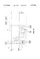
- FIG. 12illustrates a charge control unit 60 which may be used in connection with the present embodiment.
- the charge control unit 60includes a grounding switch 62 which provides a means for grounding the column line 37.
- the charge control units 60 of the present embodimentground all column lines for a discharge duration, T1, and then apply the same voltage to all column lines through equal resistances for a charge duration, T2.
- the charge durationis chosen to allow a number of the LCD elements to exceed the reference voltage, Vref, and may be controlled through the sensing of the voltage on one or more of the column lines.
- the discharge duration, charging resistance, and charge durationmay be controlled by programmable means.
- the discharging and charging of the LCD elements of the present embodimentmay be performed just prior to the refresh cycle of the LCD elements. Because the present embodiment allows sensing to occur in a relatively short time period, changes to the display caused by the sensing, which might otherwise be noticeable to a user, are greatly reduced.
- the grounding switch 62is replaced by a coupling switch which allows all of the column lines to be connected together for a duration long enough that all of the column lines reach a like voltage. This variation reduces the occurrence of surge currents through the ground terminal and also reduces total power consumption.
- the passive stylus of the present inventionmay include any object capable of changing the charge time of an LCD element.
- the stylusmay include a specialized unit which is capable of delivering additional data, such as tip switch or barrel switch condition or other data, to the host computer via an alternate method of transmission, such as an RF, ultrasonic, or infrared link.
- additional datamay then be used by the host computer, in conjunction with the touch input information, to perform applications.
- the angle of the pen with respect to horizontalmay be detected and transmitted as an infrared encoded signal, allowing the application to vary line type or width in drawing applications.
- CMCU circuitry of the present inventionmay be implemented on the glass substrate in proximity to the display elements rather than being located in the driver circuitry.
- described methods of sensing touching of elements through charge time sensingmay be implemented through sensing of discharge times for display elements.
- References to charge time sensing and measurement described hereinencompass both charging and discharging implementations.
- the term ⁇ applying a charge ⁇is defined to include both sourcing and sinking of current.
- the term ⁇ charge cycle ⁇also includes discharging cycles.
- references to ⁇ exceeding a reference voltage ⁇shall imply a more positive voltage is attained when a current is being sourced to the display element and shall imply a more negative voltage when current is being sunk from the display element.
Landscapes
- Engineering & Computer Science (AREA)
- Theoretical Computer Science (AREA)
- General Engineering & Computer Science (AREA)
- Physics & Mathematics (AREA)
- General Physics & Mathematics (AREA)
- Human Computer Interaction (AREA)
- Nonlinear Science (AREA)
- Chemical & Material Sciences (AREA)
- Crystallography & Structural Chemistry (AREA)
- Computer Hardware Design (AREA)
- Mathematical Physics (AREA)
- Optics & Photonics (AREA)
- Position Input By Displaying (AREA)
- Control Of Indicators Other Than Cathode Ray Tubes (AREA)
- Liquid Crystal Display Device Control (AREA)
- Liquid Crystal (AREA)
- Devices For Indicating Variable Information By Combining Individual Elements (AREA)
Abstract
Description
Claims (41)
Priority Applications (5)
| Application Number | Priority Date | Filing Date | Title |
|---|---|---|---|
| US08/556,689US5777596A (en) | 1995-11-13 | 1995-11-13 | Touch sensitive flat panel display |
| JP29626096AJPH09274537A (en) | 1995-11-13 | 1996-11-08 | Touch type liquid crystal display device |
| EP96308145AEP0773497B1 (en) | 1995-11-13 | 1996-11-11 | Electrically driven display and method |
| DE69614635TDE69614635T2 (en) | 1995-11-13 | 1996-11-11 | Electrically controlled display device and corresponding method |
| KR1019960053427AKR970028977A (en) | 1995-11-13 | 1996-11-12 | Touch sensitive flat panel display |
Applications Claiming Priority (1)
| Application Number | Priority Date | Filing Date | Title |
|---|---|---|---|
| US08/556,689US5777596A (en) | 1995-11-13 | 1995-11-13 | Touch sensitive flat panel display |
Publications (1)
| Publication Number | Publication Date |
|---|---|
| US5777596Atrue US5777596A (en) | 1998-07-07 |
Family
ID=24222442
Family Applications (1)
| Application Number | Title | Priority Date | Filing Date |
|---|---|---|---|
| US08/556,689Expired - LifetimeUS5777596A (en) | 1995-11-13 | 1995-11-13 | Touch sensitive flat panel display |
Country Status (5)
| Country | Link |
|---|---|
| US (1) | US5777596A (en) |
| EP (1) | EP0773497B1 (en) |
| JP (1) | JPH09274537A (en) |
| KR (1) | KR970028977A (en) |
| DE (1) | DE69614635T2 (en) |
Cited By (96)
| Publication number | Priority date | Publication date | Assignee | Title |
|---|---|---|---|---|
| US6459424B1 (en) | 1999-08-10 | 2002-10-01 | Hewlett-Packard Company | Touch-sensitive input screen having regional sensitivity and resolution properties |
| US6639587B2 (en)* | 2001-10-16 | 2003-10-28 | International Business Machines Corporation | Method and apparatus for a scaleable touch panel controller |
| US20030210235A1 (en)* | 2002-05-08 | 2003-11-13 | Roberts Jerry B. | Baselining techniques in force-based touch panel systems |
| US6661239B1 (en)* | 2001-01-02 | 2003-12-09 | Irobot Corporation | Capacitive sensor systems and methods with increased resolution and automatic calibration |
| WO2003079176A3 (en)* | 2002-03-15 | 2004-02-05 | Koninkl Philips Electronics Nv | Touch sensitive display device |
| WO2004027746A1 (en) | 2002-09-20 | 2004-04-01 | Koninklijke Philips Electronics N.V. | Luminescence and color variation compensation in a flexible display |
| WO2004053576A1 (en)* | 2002-12-12 | 2004-06-24 | Koninklijke Philips Electronics N.V. | Touch sensitive active matrix display and method for touch sensing |
| US20060125717A1 (en)* | 2002-11-28 | 2006-06-15 | Thales | Proximity detection-display device and method of using said device |
| US20060157567A1 (en)* | 2003-07-30 | 2006-07-20 | Acs Solutions Schweiz Ag | Terminal with a touch panel display and touch panel display |
| US20070152976A1 (en)* | 2005-12-30 | 2007-07-05 | Microsoft Corporation | Unintentional touch rejection |
| US20070176866A1 (en)* | 2006-01-31 | 2007-08-02 | Toppoly Optoelectronics Corp. | Display panel with image sticking elimination circuit and driving circuit with the same |
| US20070216657A1 (en)* | 2006-03-17 | 2007-09-20 | Konicek Jeffrey C | Flat panel display screen operable for touch position determination system and methods |
| US20070234492A1 (en)* | 2005-12-02 | 2007-10-11 | Irobot Corporation | Coverage robot mobility |
| US20070252005A1 (en)* | 2006-05-01 | 2007-11-01 | Konicek Jeffrey C | Active matrix emissive display and optical scanner system, methods and applications |
| US20070279332A1 (en)* | 2004-02-20 | 2007-12-06 | Fryer Christopher J N | Display Activated by the Presence of a User |
| US20080062147A1 (en)* | 2006-06-09 | 2008-03-13 | Hotelling Steve P | Touch screen liquid crystal display |
| US20080062140A1 (en)* | 2006-06-09 | 2008-03-13 | Apple Inc. | Touch screen liquid crystal display |
| US20080074375A1 (en)* | 2006-09-21 | 2008-03-27 | Samsung Electronics Co., Ltd. | Sequence control unit, driving method thereof, and liquid crystal display device having the same |
| US20080117181A1 (en)* | 2006-11-21 | 2008-05-22 | Jong-Woung Park | Display device and driving method thereof |
| US20080129898A1 (en)* | 2006-11-09 | 2008-06-05 | Samsung Electronics Co., Ltd. | LCDS with integrated touch panels |
| US20080143689A1 (en)* | 2006-12-18 | 2008-06-19 | Foo Ken K | Optical shuttered touchscreen and method therefor |
| US20080229885A1 (en)* | 2007-03-22 | 2008-09-25 | Mah Pat Y | Jar opener |
| US20080309627A1 (en)* | 2007-06-13 | 2008-12-18 | Apple Inc. | Integrated in-plane switching |
| US20090074255A1 (en)* | 2007-09-18 | 2009-03-19 | Motorola, Inc. | Apparatus and method for capturing skin texture biometric in electronic devices |
| US20090079707A1 (en)* | 2007-09-24 | 2009-03-26 | Motorola, Inc. | Integrated capacitive sensing devices and methods |
| US20090201259A1 (en)* | 2008-02-07 | 2009-08-13 | Nokia Corporation | Cursor creation for touch screen |
| US20090212642A1 (en)* | 2008-02-25 | 2009-08-27 | Apple Inc. | Charge recycling for multi-touch controllers |
| US20090318229A1 (en)* | 2008-06-20 | 2009-12-24 | James Zielinski | Capacitive touchpad and toy incorporating the same |
| US20100060600A1 (en)* | 2008-09-05 | 2010-03-11 | Zheng Wang | Array substrate, liquid crystal display comprising the same, and method for manufacturing the same |
| US20100214248A1 (en)* | 2009-02-25 | 2010-08-26 | Seiko Epson Corporation | Display apparatus with touch sensor function |
| US20100282525A1 (en)* | 2009-05-11 | 2010-11-11 | Stewart Bradley C | Capacitive Touchpad Method Using MCU GPIO and Signal Processing |
| US8239992B2 (en) | 2007-05-09 | 2012-08-14 | Irobot Corporation | Compact autonomous coverage robot |
| US8253368B2 (en) | 2004-01-28 | 2012-08-28 | Irobot Corporation | Debris sensor for cleaning apparatus |
| US8363033B2 (en) | 2010-03-08 | 2013-01-29 | Chunghwa Picture Tubes, Ltd. | Capacitance sensing circuit |
| US8368339B2 (en) | 2001-01-24 | 2013-02-05 | Irobot Corporation | Robot confinement |
| US8374721B2 (en) | 2005-12-02 | 2013-02-12 | Irobot Corporation | Robot system |
| US8380350B2 (en) | 2005-12-02 | 2013-02-19 | Irobot Corporation | Autonomous coverage robot navigation system |
| US8382906B2 (en) | 2005-02-18 | 2013-02-26 | Irobot Corporation | Autonomous surface cleaning robot for wet cleaning |
| US8386081B2 (en) | 2002-09-13 | 2013-02-26 | Irobot Corporation | Navigational control system for a robotic device |
| US8390251B2 (en) | 2004-01-21 | 2013-03-05 | Irobot Corporation | Autonomous robot auto-docking and energy management systems and methods |
| US8387193B2 (en) | 2005-02-18 | 2013-03-05 | Irobot Corporation | Autonomous surface cleaning robot for wet and dry cleaning |
| US8396592B2 (en) | 2001-06-12 | 2013-03-12 | Irobot Corporation | Method and system for multi-mode coverage for an autonomous robot |
| US8412377B2 (en) | 2000-01-24 | 2013-04-02 | Irobot Corporation | Obstacle following sensor scheme for a mobile robot |
| US8417383B2 (en) | 2006-05-31 | 2013-04-09 | Irobot Corporation | Detecting robot stasis |
| US8416209B2 (en) | 2004-05-06 | 2013-04-09 | Apple Inc. | Multipoint touchscreen |
| US8418303B2 (en) | 2006-05-19 | 2013-04-16 | Irobot Corporation | Cleaning robot roller processing |
| US8428778B2 (en) | 2002-09-13 | 2013-04-23 | Irobot Corporation | Navigational control system for a robotic device |
| US8432371B2 (en) | 2006-06-09 | 2013-04-30 | Apple Inc. | Touch screen liquid crystal display |
| US8463438B2 (en) | 2001-06-12 | 2013-06-11 | Irobot Corporation | Method and system for multi-mode coverage for an autonomous robot |
| US8474090B2 (en) | 2002-01-03 | 2013-07-02 | Irobot Corporation | Autonomous floor-cleaning robot |
| US8493330B2 (en) | 2007-01-03 | 2013-07-23 | Apple Inc. | Individual channel phase delay scheme |
| US8515578B2 (en) | 2002-09-13 | 2013-08-20 | Irobot Corporation | Navigational control system for a robotic device |
| US8584305B2 (en) | 2005-12-02 | 2013-11-19 | Irobot Corporation | Modular robot |
| US8594840B1 (en) | 2004-07-07 | 2013-11-26 | Irobot Corporation | Celestial navigation system for an autonomous robot |
| US8743300B2 (en) | 2010-12-22 | 2014-06-03 | Apple Inc. | Integrated touch screens |
| US8739355B2 (en) | 2005-02-18 | 2014-06-03 | Irobot Corporation | Autonomous surface cleaning robot for dry cleaning |
| US8780342B2 (en) | 2004-03-29 | 2014-07-15 | Irobot Corporation | Methods and apparatus for position estimation using reflected light sources |
| US8788092B2 (en) | 2000-01-24 | 2014-07-22 | Irobot Corporation | Obstacle following sensor scheme for a mobile robot |
| US8800107B2 (en) | 2010-02-16 | 2014-08-12 | Irobot Corporation | Vacuum brush |
| US8930023B2 (en) | 2009-11-06 | 2015-01-06 | Irobot Corporation | Localization by learning of wave-signal distributions |
| US8972052B2 (en) | 2004-07-07 | 2015-03-03 | Irobot Corporation | Celestial navigation system for an autonomous vehicle |
| US8970537B1 (en) | 2013-09-30 | 2015-03-03 | Synaptics Incorporated | Matrix sensor for image touch sensing |
| US9008835B2 (en) | 2004-06-24 | 2015-04-14 | Irobot Corporation | Remote control scheduler and method for autonomous robotic device |
| US9081457B2 (en) | 2013-10-30 | 2015-07-14 | Synaptics Incorporated | Single-layer muti-touch capacitive imaging sensor |
| US9081453B2 (en) | 2012-01-12 | 2015-07-14 | Synaptics Incorporated | Single layer capacitive imaging sensors |
| US9274662B2 (en) | 2013-10-18 | 2016-03-01 | Synaptics Incorporated | Sensor matrix pad for performing multiple capacitive sensing techniques |
| US9298325B2 (en) | 2013-09-30 | 2016-03-29 | Synaptics Incorporated | Processing system for a capacitive sensing device |
| US9310994B2 (en) | 2010-02-19 | 2016-04-12 | Microsoft Technology Licensing, Llc | Use of bezel as an input mechanism |
| US9320398B2 (en) | 2005-12-02 | 2016-04-26 | Irobot Corporation | Autonomous coverage robots |
| US9367205B2 (en) | 2010-02-19 | 2016-06-14 | Microsoft Technolgoy Licensing, Llc | Radial menus with bezel gestures |
| US9411498B2 (en) | 2010-01-28 | 2016-08-09 | Microsoft Technology Licensing, Llc | Brush, carbon-copy, and fill gestures |
| US9454304B2 (en) | 2010-02-25 | 2016-09-27 | Microsoft Technology Licensing, Llc | Multi-screen dual tap gesture |
| US9459367B2 (en) | 2013-10-02 | 2016-10-04 | Synaptics Incorporated | Capacitive sensor driving technique that enables hybrid sensing or equalization |
| US9477337B2 (en) | 2014-03-14 | 2016-10-25 | Microsoft Technology Licensing, Llc | Conductive trace routing for display and bezel sensors |
| US9519356B2 (en) | 2010-02-04 | 2016-12-13 | Microsoft Technology Licensing, Llc | Link gestures |
| US9542023B2 (en) | 2013-08-07 | 2017-01-10 | Synaptics Incorporated | Capacitive sensing using matrix electrodes driven by routing traces disposed in a source line layer |
| US9582122B2 (en) | 2012-11-12 | 2017-02-28 | Microsoft Technology Licensing, Llc | Touch-sensitive bezel techniques |
| CN103870088B (en)* | 2008-07-03 | 2017-05-03 | 苹果公司 | Display with dual-function capacitive elements |
| US9690397B2 (en) | 2014-05-20 | 2017-06-27 | Synaptics Incorporated | System and method for detecting an active pen with a matrix sensor |
| US9710095B2 (en) | 2007-01-05 | 2017-07-18 | Apple Inc. | Touch screen stack-ups |
| US9715304B2 (en) | 2015-06-30 | 2017-07-25 | Synaptics Incorporated | Regular via pattern for sensor-based input device |
| US9720541B2 (en) | 2015-06-30 | 2017-08-01 | Synaptics Incorporated | Arrangement of sensor pads and display driver pads for input device |
| US9778713B2 (en) | 2015-01-05 | 2017-10-03 | Synaptics Incorporated | Modulating a reference voltage to preform capacitive sensing |
| US9798429B2 (en) | 2014-02-28 | 2017-10-24 | Synaptics Incorporated | Guard electrodes in a sensing stack |
| US9857970B2 (en) | 2010-01-28 | 2018-01-02 | Microsoft Technology Licensing, Llc | Copy and staple gestures |
| US9927832B2 (en) | 2014-04-25 | 2018-03-27 | Synaptics Incorporated | Input device having a reduced border region |
| US9939972B2 (en) | 2015-04-06 | 2018-04-10 | Synaptics Incorporated | Matrix sensor with via routing |
| US9965165B2 (en) | 2010-02-19 | 2018-05-08 | Microsoft Technology Licensing, Llc | Multi-finger gestures |
| US10037112B2 (en) | 2015-09-30 | 2018-07-31 | Synaptics Incorporated | Sensing an active device'S transmission using timing interleaved with display updates |
| US10042489B2 (en) | 2013-09-30 | 2018-08-07 | Synaptics Incorporated | Matrix sensor for image touch sensing |
| US10067587B2 (en) | 2015-12-29 | 2018-09-04 | Synaptics Incorporated | Routing conductors in an integrated display device and sensing device |
| US10095948B2 (en) | 2015-06-30 | 2018-10-09 | Synaptics Incorporated | Modulation scheme for fingerprint sensing |
| US10126890B2 (en) | 2015-12-31 | 2018-11-13 | Synaptics Incorporated | Single layer sensor pattern and sensing method |
| US10133421B2 (en) | 2014-04-02 | 2018-11-20 | Synaptics Incorporated | Display stackups for matrix sensor |
| US10175827B2 (en) | 2014-12-23 | 2019-01-08 | Synaptics Incorporated | Detecting an active pen using a capacitive sensing device |
| US10488994B2 (en) | 2015-09-07 | 2019-11-26 | Synaptics Incorporated | Single layer capacitive sensor pattern |
Families Citing this family (27)
| Publication number | Priority date | Publication date | Assignee | Title |
|---|---|---|---|---|
| KR20020080160A (en)* | 2001-04-12 | 2002-10-23 | 에프디테크 주식회사 | A driving circuit of a resistive touch screen |
| US7053967B2 (en) | 2002-05-23 | 2006-05-30 | Planar Systems, Inc. | Light sensitive display |
| AU2002336341A1 (en) | 2002-02-20 | 2003-09-09 | Planar Systems, Inc. | Light sensitive display |
| US7009663B2 (en) | 2003-12-17 | 2006-03-07 | Planar Systems, Inc. | Integrated optical light sensitive active matrix liquid crystal display |
| CN1672121A (en) | 2002-08-01 | 2005-09-21 | 皇家飞利浦电子股份有限公司 | Touch sensitive display device |
| US7388571B2 (en) | 2002-11-21 | 2008-06-17 | Research In Motion Limited | System and method of integrating a touchscreen within an LCD |
| JP2006513501A (en)* | 2003-01-20 | 2006-04-20 | コーニンクレッカ フィリップス エレクトロニクス エヌ ヴィ | Touch sensitive display |
| US20080084374A1 (en) | 2003-02-20 | 2008-04-10 | Planar Systems, Inc. | Light sensitive display |
| KR101152136B1 (en)* | 2005-10-26 | 2012-06-15 | 삼성전자주식회사 | Touch sensible display device |
| KR101230309B1 (en) | 2006-01-27 | 2013-02-06 | 삼성디스플레이 주식회사 | Display device and processing apparatus of sensing signal |
| KR100601152B1 (en)* | 2006-03-21 | 2006-07-19 | (주) 넥스트칩 | Touch sensing device and method using charge sharing |
| JP4510049B2 (en)* | 2007-04-24 | 2010-07-21 | 三菱電機株式会社 | Pressure detection digitizer |
| KR100933037B1 (en)* | 2009-04-22 | 2009-12-21 | 에이디반도체(주) | Multi-Touch Resistive Touch Screen Recognizing Multi-Touch Coordinates Through Capacitor Charging Time |
| US9310923B2 (en) | 2010-12-03 | 2016-04-12 | Apple Inc. | Input device for touch sensitive devices |
| US8928635B2 (en) | 2011-06-22 | 2015-01-06 | Apple Inc. | Active stylus |
| US9329703B2 (en) | 2011-06-22 | 2016-05-03 | Apple Inc. | Intelligent stylus |
| US8988388B2 (en) | 2011-09-16 | 2015-03-24 | Htc Corporation | Electronic device and method for scanning a touch panel thereof |
| JP2013242699A (en)* | 2012-05-21 | 2013-12-05 | Renesas Electronics Corp | Semiconductor device |
| US9652090B2 (en) | 2012-07-27 | 2017-05-16 | Apple Inc. | Device for digital communication through capacitive coupling |
| US9557845B2 (en) | 2012-07-27 | 2017-01-31 | Apple Inc. | Input device for and method of communication with capacitive devices through frequency variation |
| US9176604B2 (en) | 2012-07-27 | 2015-11-03 | Apple Inc. | Stylus device |
| US10048775B2 (en) | 2013-03-14 | 2018-08-14 | Apple Inc. | Stylus detection and demodulation |
| US10067580B2 (en) | 2013-07-31 | 2018-09-04 | Apple Inc. | Active stylus for use with touch controller architecture |
| US10067618B2 (en) | 2014-12-04 | 2018-09-04 | Apple Inc. | Coarse scan and targeted active mode scan for touch |
| CN108351720B (en)* | 2015-11-25 | 2021-05-04 | 夏普株式会社 | Capacitance detection method, position detection method, touch panel controller, and electronic device |
| US10474277B2 (en) | 2016-05-31 | 2019-11-12 | Apple Inc. | Position-based stylus communication |
| US12153764B1 (en) | 2020-09-25 | 2024-11-26 | Apple Inc. | Stylus with receive architecture for position determination |
Citations (20)
| Publication number | Priority date | Publication date | Assignee | Title |
|---|---|---|---|---|
| US4224615A (en)* | 1978-09-14 | 1980-09-23 | Texas Instruments Incorporated | Method of using a liquid crystal display device as a data input device |
| US4363029A (en)* | 1980-11-17 | 1982-12-07 | Texas Instruments Incorporated | Switch for sensing proximity of an operator |
| US4529968A (en)* | 1981-11-16 | 1985-07-16 | The Secretary Of State For Defence In Her Britannic Majesty's Government Of The United Kingdom Of Great Britain And Northern Ireland | Touch sensitive liquid crystal switch |
| JPS61156107A (en)* | 1984-12-28 | 1986-07-15 | Canon Inc | Liquid crystal display device |
| US4736191A (en)* | 1985-08-02 | 1988-04-05 | Karl E. Matzke | Touch activated control method and apparatus |
| US5043710A (en)* | 1988-06-08 | 1991-08-27 | Jaeger | Key making use of the properties of a liquid crystal |
| FR2662528A1 (en)* | 1990-05-25 | 1991-11-29 | Sextant Avionique | Device for locating an object situated in proximity to a detection area and transparent keyboard using the said device |
| US5194862A (en)* | 1990-06-29 | 1993-03-16 | U.S. Philips Corporation | Touch sensor array systems and display systems incorporating such |
| EP0546704A2 (en)* | 1991-12-13 | 1993-06-16 | AT&T Corp. | Intelligent work surfaces |
| EP0568342A1 (en)* | 1992-04-30 | 1993-11-03 | Varintelligent(BVI)Limited | A touch sensitive device |
| US5267066A (en)* | 1991-03-27 | 1993-11-30 | Sharp Kabushiki Kaisha | Liquid crystal display device, method of correcting defective pixels, and defective-pixel correcting apparatus used therein |
| JPH0634940A (en)* | 1992-07-21 | 1994-02-10 | Rohm Co Ltd | Liquid crystal display device |
| EP0622754A1 (en)* | 1993-04-30 | 1994-11-02 | Sharp Kabushiki Kaisha | Display-integrated type tablet device with high co-ordinate detection accuracy and method for driving the same |
| US5451724A (en)* | 1992-08-05 | 1995-09-19 | Fujitsu Limited | Touch panel for detecting a coordinate of an arbitrary position where pressure is applied |
| US5457289A (en)* | 1994-03-16 | 1995-10-10 | Microtouch Systems, Inc. | Frontally shielded capacitive touch sensor system |
| US5459463A (en)* | 1990-05-25 | 1995-10-17 | Sextant Avionique | Device for locating an object situated close to a detection area and a transparent keyboard using said device |
| US5495077A (en)* | 1992-06-08 | 1996-02-27 | Synaptics, Inc. | Object position and proximity detector |
| US5500937A (en)* | 1993-09-08 | 1996-03-19 | Apple Computer, Inc. | Method and apparatus for editing an inked object while simultaneously displaying its recognized object |
| US5510813A (en)* | 1993-08-26 | 1996-04-23 | U.S. Philips Corporation | Data processing device comprising a touch screen and a force sensor |
| US5528266A (en)* | 1989-05-15 | 1996-06-18 | International Business Machines Corporation | Flat touch screen workpad for a data processing system |
- 1995
- 1995-11-13USUS08/556,689patent/US5777596A/ennot_activeExpired - Lifetime
- 1996
- 1996-11-08JPJP29626096Apatent/JPH09274537A/enactivePending
- 1996-11-11DEDE69614635Tpatent/DE69614635T2/ennot_activeExpired - Lifetime
- 1996-11-11EPEP96308145Apatent/EP0773497B1/ennot_activeExpired - Lifetime
- 1996-11-12KRKR1019960053427Apatent/KR970028977A/ennot_activeCeased
Patent Citations (20)
| Publication number | Priority date | Publication date | Assignee | Title |
|---|---|---|---|---|
| US4224615A (en)* | 1978-09-14 | 1980-09-23 | Texas Instruments Incorporated | Method of using a liquid crystal display device as a data input device |
| US4363029A (en)* | 1980-11-17 | 1982-12-07 | Texas Instruments Incorporated | Switch for sensing proximity of an operator |
| US4529968A (en)* | 1981-11-16 | 1985-07-16 | The Secretary Of State For Defence In Her Britannic Majesty's Government Of The United Kingdom Of Great Britain And Northern Ireland | Touch sensitive liquid crystal switch |
| JPS61156107A (en)* | 1984-12-28 | 1986-07-15 | Canon Inc | Liquid crystal display device |
| US4736191A (en)* | 1985-08-02 | 1988-04-05 | Karl E. Matzke | Touch activated control method and apparatus |
| US5043710A (en)* | 1988-06-08 | 1991-08-27 | Jaeger | Key making use of the properties of a liquid crystal |
| US5528266A (en)* | 1989-05-15 | 1996-06-18 | International Business Machines Corporation | Flat touch screen workpad for a data processing system |
| US5459463A (en)* | 1990-05-25 | 1995-10-17 | Sextant Avionique | Device for locating an object situated close to a detection area and a transparent keyboard using said device |
| FR2662528A1 (en)* | 1990-05-25 | 1991-11-29 | Sextant Avionique | Device for locating an object situated in proximity to a detection area and transparent keyboard using the said device |
| US5194862A (en)* | 1990-06-29 | 1993-03-16 | U.S. Philips Corporation | Touch sensor array systems and display systems incorporating such |
| US5267066A (en)* | 1991-03-27 | 1993-11-30 | Sharp Kabushiki Kaisha | Liquid crystal display device, method of correcting defective pixels, and defective-pixel correcting apparatus used therein |
| EP0546704A2 (en)* | 1991-12-13 | 1993-06-16 | AT&T Corp. | Intelligent work surfaces |
| EP0568342A1 (en)* | 1992-04-30 | 1993-11-03 | Varintelligent(BVI)Limited | A touch sensitive device |
| US5495077A (en)* | 1992-06-08 | 1996-02-27 | Synaptics, Inc. | Object position and proximity detector |
| JPH0634940A (en)* | 1992-07-21 | 1994-02-10 | Rohm Co Ltd | Liquid crystal display device |
| US5451724A (en)* | 1992-08-05 | 1995-09-19 | Fujitsu Limited | Touch panel for detecting a coordinate of an arbitrary position where pressure is applied |
| EP0622754A1 (en)* | 1993-04-30 | 1994-11-02 | Sharp Kabushiki Kaisha | Display-integrated type tablet device with high co-ordinate detection accuracy and method for driving the same |
| US5510813A (en)* | 1993-08-26 | 1996-04-23 | U.S. Philips Corporation | Data processing device comprising a touch screen and a force sensor |
| US5500937A (en)* | 1993-09-08 | 1996-03-19 | Apple Computer, Inc. | Method and apparatus for editing an inked object while simultaneously displaying its recognized object |
| US5457289A (en)* | 1994-03-16 | 1995-10-10 | Microtouch Systems, Inc. | Frontally shielded capacitive touch sensor system |
Cited By (245)
| Publication number | Priority date | Publication date | Assignee | Title |
|---|---|---|---|---|
| US6459424B1 (en) | 1999-08-10 | 2002-10-01 | Hewlett-Packard Company | Touch-sensitive input screen having regional sensitivity and resolution properties |
| US8565920B2 (en) | 2000-01-24 | 2013-10-22 | Irobot Corporation | Obstacle following sensor scheme for a mobile robot |
| US8788092B2 (en) | 2000-01-24 | 2014-07-22 | Irobot Corporation | Obstacle following sensor scheme for a mobile robot |
| US9446521B2 (en) | 2000-01-24 | 2016-09-20 | Irobot Corporation | Obstacle following sensor scheme for a mobile robot |
| US8412377B2 (en) | 2000-01-24 | 2013-04-02 | Irobot Corporation | Obstacle following sensor scheme for a mobile robot |
| US8761935B2 (en) | 2000-01-24 | 2014-06-24 | Irobot Corporation | Obstacle following sensor scheme for a mobile robot |
| US8478442B2 (en) | 2000-01-24 | 2013-07-02 | Irobot Corporation | Obstacle following sensor scheme for a mobile robot |
| US9144361B2 (en) | 2000-04-04 | 2015-09-29 | Irobot Corporation | Debris sensor for cleaning apparatus |
| US6661239B1 (en)* | 2001-01-02 | 2003-12-09 | Irobot Corporation | Capacitive sensor systems and methods with increased resolution and automatic calibration |
| US8368339B2 (en) | 2001-01-24 | 2013-02-05 | Irobot Corporation | Robot confinement |
| US9622635B2 (en) | 2001-01-24 | 2017-04-18 | Irobot Corporation | Autonomous floor-cleaning robot |
| US9582005B2 (en) | 2001-01-24 | 2017-02-28 | Irobot Corporation | Robot confinement |
| US8686679B2 (en) | 2001-01-24 | 2014-04-01 | Irobot Corporation | Robot confinement |
| US9038233B2 (en) | 2001-01-24 | 2015-05-26 | Irobot Corporation | Autonomous floor-cleaning robot |
| US9167946B2 (en) | 2001-01-24 | 2015-10-27 | Irobot Corporation | Autonomous floor cleaning robot |
| US9104204B2 (en) | 2001-06-12 | 2015-08-11 | Irobot Corporation | Method and system for multi-mode coverage for an autonomous robot |
| US8396592B2 (en) | 2001-06-12 | 2013-03-12 | Irobot Corporation | Method and system for multi-mode coverage for an autonomous robot |
| US8463438B2 (en) | 2001-06-12 | 2013-06-11 | Irobot Corporation | Method and system for multi-mode coverage for an autonomous robot |
| US6639587B2 (en)* | 2001-10-16 | 2003-10-28 | International Business Machines Corporation | Method and apparatus for a scaleable touch panel controller |
| US8516651B2 (en) | 2002-01-03 | 2013-08-27 | Irobot Corporation | Autonomous floor-cleaning robot |
| US8474090B2 (en) | 2002-01-03 | 2013-07-02 | Irobot Corporation | Autonomous floor-cleaning robot |
| US9128486B2 (en) | 2002-01-24 | 2015-09-08 | Irobot Corporation | Navigational control system for a robotic device |
| WO2003079176A3 (en)* | 2002-03-15 | 2004-02-05 | Koninkl Philips Electronics Nv | Touch sensitive display device |
| US7532202B2 (en)* | 2002-05-08 | 2009-05-12 | 3M Innovative Properties Company | Baselining techniques in force-based touch panel systems |
| US20030210235A1 (en)* | 2002-05-08 | 2003-11-13 | Roberts Jerry B. | Baselining techniques in force-based touch panel systems |
| US8386081B2 (en) | 2002-09-13 | 2013-02-26 | Irobot Corporation | Navigational control system for a robotic device |
| US8793020B2 (en) | 2002-09-13 | 2014-07-29 | Irobot Corporation | Navigational control system for a robotic device |
| US8781626B2 (en) | 2002-09-13 | 2014-07-15 | Irobot Corporation | Navigational control system for a robotic device |
| US9949608B2 (en) | 2002-09-13 | 2018-04-24 | Irobot Corporation | Navigational control system for a robotic device |
| US8515578B2 (en) | 2002-09-13 | 2013-08-20 | Irobot Corporation | Navigational control system for a robotic device |
| US8428778B2 (en) | 2002-09-13 | 2013-04-23 | Irobot Corporation | Navigational control system for a robotic device |
| WO2004027746A1 (en) | 2002-09-20 | 2004-04-01 | Koninklijke Philips Electronics N.V. | Luminescence and color variation compensation in a flexible display |
| CN100409300C (en)* | 2002-09-20 | 2008-08-06 | 皇家飞利浦电子股份有限公司 | Brightness and color variation compensation for flexible displays |
| KR100977942B1 (en)* | 2002-09-20 | 2010-08-24 | 코닌클리즈케 필립스 일렉트로닉스 엔.브이. | Compensation device and method, flexible display and portable device |
| US7663611B2 (en)* | 2002-11-28 | 2010-02-16 | Thales | Display device with proximity detection and method of using said device |
| US20060125717A1 (en)* | 2002-11-28 | 2006-06-15 | Thales | Proximity detection-display device and method of using said device |
| US20060012575A1 (en)* | 2002-12-12 | 2006-01-19 | Koninklijke Philips Electronics N.V. | Touch sensitive active matrix display and method for touch sensing |
| WO2004053576A1 (en)* | 2002-12-12 | 2004-06-24 | Koninklijke Philips Electronics N.V. | Touch sensitive active matrix display and method for touch sensing |
| US20060157567A1 (en)* | 2003-07-30 | 2006-07-20 | Acs Solutions Schweiz Ag | Terminal with a touch panel display and touch panel display |
| US8749196B2 (en) | 2004-01-21 | 2014-06-10 | Irobot Corporation | Autonomous robot auto-docking and energy management systems and methods |
| US8390251B2 (en) | 2004-01-21 | 2013-03-05 | Irobot Corporation | Autonomous robot auto-docking and energy management systems and methods |
| US8461803B2 (en) | 2004-01-21 | 2013-06-11 | Irobot Corporation | Autonomous robot auto-docking and energy management systems and methods |
| US8854001B2 (en) | 2004-01-21 | 2014-10-07 | Irobot Corporation | Autonomous robot auto-docking and energy management systems and methods |
| US9215957B2 (en) | 2004-01-21 | 2015-12-22 | Irobot Corporation | Autonomous robot auto-docking and energy management systems and methods |
| US8598829B2 (en) | 2004-01-28 | 2013-12-03 | Irobot Corporation | Debris sensor for cleaning apparatus |
| US8456125B2 (en) | 2004-01-28 | 2013-06-04 | Irobot Corporation | Debris sensor for cleaning apparatus |
| US8378613B2 (en) | 2004-01-28 | 2013-02-19 | Irobot Corporation | Debris sensor for cleaning apparatus |
| US8253368B2 (en) | 2004-01-28 | 2012-08-28 | Irobot Corporation | Debris sensor for cleaning apparatus |
| US20070279332A1 (en)* | 2004-02-20 | 2007-12-06 | Fryer Christopher J N | Display Activated by the Presence of a User |
| US8780342B2 (en) | 2004-03-29 | 2014-07-15 | Irobot Corporation | Methods and apparatus for position estimation using reflected light sources |
| US9360300B2 (en) | 2004-03-29 | 2016-06-07 | Irobot Corporation | Methods and apparatus for position estimation using reflected light sources |
| US8872785B2 (en) | 2004-05-06 | 2014-10-28 | Apple Inc. | Multipoint touchscreen |
| US10331259B2 (en) | 2004-05-06 | 2019-06-25 | Apple Inc. | Multipoint touchscreen |
| US8416209B2 (en) | 2004-05-06 | 2013-04-09 | Apple Inc. | Multipoint touchscreen |
| US11604547B2 (en) | 2004-05-06 | 2023-03-14 | Apple Inc. | Multipoint touchscreen |
| US10908729B2 (en) | 2004-05-06 | 2021-02-02 | Apple Inc. | Multipoint touchscreen |
| US8928618B2 (en) | 2004-05-06 | 2015-01-06 | Apple Inc. | Multipoint touchscreen |
| US8982087B2 (en) | 2004-05-06 | 2015-03-17 | Apple Inc. | Multipoint touchscreen |
| US9454277B2 (en) | 2004-05-06 | 2016-09-27 | Apple Inc. | Multipoint touchscreen |
| US9035907B2 (en) | 2004-05-06 | 2015-05-19 | Apple Inc. | Multipoint touchscreen |
| US8605051B2 (en) | 2004-05-06 | 2013-12-10 | Apple Inc. | Multipoint touchscreen |
| US9486924B2 (en) | 2004-06-24 | 2016-11-08 | Irobot Corporation | Remote control scheduler and method for autonomous robotic device |
| US9008835B2 (en) | 2004-06-24 | 2015-04-14 | Irobot Corporation | Remote control scheduler and method for autonomous robotic device |
| US8594840B1 (en) | 2004-07-07 | 2013-11-26 | Irobot Corporation | Celestial navigation system for an autonomous robot |
| US8634956B1 (en) | 2004-07-07 | 2014-01-21 | Irobot Corporation | Celestial navigation system for an autonomous robot |
| US9229454B1 (en) | 2004-07-07 | 2016-01-05 | Irobot Corporation | Autonomous mobile robot system |
| US8874264B1 (en) | 2004-07-07 | 2014-10-28 | Irobot Corporation | Celestial navigation system for an autonomous robot |
| US9223749B2 (en) | 2004-07-07 | 2015-12-29 | Irobot Corporation | Celestial navigation system for an autonomous vehicle |
| US8972052B2 (en) | 2004-07-07 | 2015-03-03 | Irobot Corporation | Celestial navigation system for an autonomous vehicle |
| US8382906B2 (en) | 2005-02-18 | 2013-02-26 | Irobot Corporation | Autonomous surface cleaning robot for wet cleaning |
| US8782848B2 (en) | 2005-02-18 | 2014-07-22 | Irobot Corporation | Autonomous surface cleaning robot for dry cleaning |
| US8774966B2 (en) | 2005-02-18 | 2014-07-08 | Irobot Corporation | Autonomous surface cleaning robot for wet and dry cleaning |
| US8985127B2 (en) | 2005-02-18 | 2015-03-24 | Irobot Corporation | Autonomous surface cleaning robot for wet cleaning |
| US8392021B2 (en) | 2005-02-18 | 2013-03-05 | Irobot Corporation | Autonomous surface cleaning robot for wet cleaning |
| US8739355B2 (en) | 2005-02-18 | 2014-06-03 | Irobot Corporation | Autonomous surface cleaning robot for dry cleaning |
| US8670866B2 (en) | 2005-02-18 | 2014-03-11 | Irobot Corporation | Autonomous surface cleaning robot for wet and dry cleaning |
| US8387193B2 (en) | 2005-02-18 | 2013-03-05 | Irobot Corporation | Autonomous surface cleaning robot for wet and dry cleaning |
| US10470629B2 (en) | 2005-02-18 | 2019-11-12 | Irobot Corporation | Autonomous surface cleaning robot for dry cleaning |
| US9445702B2 (en) | 2005-02-18 | 2016-09-20 | Irobot Corporation | Autonomous surface cleaning robot for wet and dry cleaning |
| US8855813B2 (en) | 2005-02-18 | 2014-10-07 | Irobot Corporation | Autonomous surface cleaning robot for wet and dry cleaning |
| US8966707B2 (en) | 2005-02-18 | 2015-03-03 | Irobot Corporation | Autonomous surface cleaning robot for dry cleaning |
| US8584307B2 (en) | 2005-12-02 | 2013-11-19 | Irobot Corporation | Modular robot |
| US9320398B2 (en) | 2005-12-02 | 2016-04-26 | Irobot Corporation | Autonomous coverage robots |
| US8950038B2 (en) | 2005-12-02 | 2015-02-10 | Irobot Corporation | Modular robot |
| US8374721B2 (en) | 2005-12-02 | 2013-02-12 | Irobot Corporation | Robot system |
| US8380350B2 (en) | 2005-12-02 | 2013-02-19 | Irobot Corporation | Autonomous coverage robot navigation system |
| US7441298B2 (en) | 2005-12-02 | 2008-10-28 | Irobot Corporation | Coverage robot mobility |
| US10524629B2 (en) | 2005-12-02 | 2020-01-07 | Irobot Corporation | Modular Robot |
| US20070234492A1 (en)* | 2005-12-02 | 2007-10-11 | Irobot Corporation | Coverage robot mobility |
| US8978196B2 (en) | 2005-12-02 | 2015-03-17 | Irobot Corporation | Coverage robot mobility |
| US8584305B2 (en) | 2005-12-02 | 2013-11-19 | Irobot Corporation | Modular robot |
| US8954192B2 (en) | 2005-12-02 | 2015-02-10 | Irobot Corporation | Navigating autonomous coverage robots |
| US9144360B2 (en) | 2005-12-02 | 2015-09-29 | Irobot Corporation | Autonomous coverage robot navigation system |
| US9599990B2 (en) | 2005-12-02 | 2017-03-21 | Irobot Corporation | Robot system |
| US8600553B2 (en) | 2005-12-02 | 2013-12-03 | Irobot Corporation | Coverage robot mobility |
| US9149170B2 (en) | 2005-12-02 | 2015-10-06 | Irobot Corporation | Navigating autonomous coverage robots |
| US8606401B2 (en) | 2005-12-02 | 2013-12-10 | Irobot Corporation | Autonomous coverage robot navigation system |
| US8761931B2 (en) | 2005-12-02 | 2014-06-24 | Irobot Corporation | Robot system |
| US8661605B2 (en) | 2005-12-02 | 2014-03-04 | Irobot Corporation | Coverage robot mobility |
| US9392920B2 (en) | 2005-12-02 | 2016-07-19 | Irobot Corporation | Robot system |
| US10019080B2 (en) | 2005-12-30 | 2018-07-10 | Microsoft Technology Licensing, Llc | Unintentional touch rejection |
| US9952718B2 (en) | 2005-12-30 | 2018-04-24 | Microsoft Technology Licensing, Llc | Unintentional touch rejection |
| US8018440B2 (en) | 2005-12-30 | 2011-09-13 | Microsoft Corporation | Unintentional touch rejection |
| US9594457B2 (en) | 2005-12-30 | 2017-03-14 | Microsoft Technology Licensing, Llc | Unintentional touch rejection |
| US8659570B2 (en) | 2005-12-30 | 2014-02-25 | Microsoft Corporation | Unintentional touch rejection |
| US8294686B2 (en) | 2005-12-30 | 2012-10-23 | Microsoft Corporation | Unintentional touch rejection |
| US9946370B2 (en) | 2005-12-30 | 2018-04-17 | Microsoft Technology Licensing, Llc | Unintentional touch rejection |
| US9261964B2 (en) | 2005-12-30 | 2016-02-16 | Microsoft Technology Licensing, Llc | Unintentional touch rejection |
| US20070152976A1 (en)* | 2005-12-30 | 2007-07-05 | Microsoft Corporation | Unintentional touch rejection |
| US8040309B2 (en)* | 2006-01-31 | 2011-10-18 | Chimei Innolux Corproation | Display panel with image sticking elimination circuit and driving circuit with the same |
| US20070176866A1 (en)* | 2006-01-31 | 2007-08-02 | Toppoly Optoelectronics Corp. | Display panel with image sticking elimination circuit and driving circuit with the same |
| US20140009439A1 (en)* | 2006-03-17 | 2014-01-09 | Jeffrey C. Konicek | Flat Panel Display Screen Operable For Touch Position Prediction Methods |
| US8519978B2 (en) | 2006-03-17 | 2013-08-27 | Jeffrey Konicek | Flat panel display screen operable for touch position determination system and methods |
| US9207797B2 (en)* | 2006-03-17 | 2015-12-08 | Jeffrey C. Konicek | Flat panel display screen operable for touch position prediction methods |
| US8144115B2 (en)* | 2006-03-17 | 2012-03-27 | Konicek Jeffrey C | Flat panel display screen operable for touch position determination system and methods |
| US20070216657A1 (en)* | 2006-03-17 | 2007-09-20 | Konicek Jeffrey C | Flat panel display screen operable for touch position determination system and methods |
| US20070252005A1 (en)* | 2006-05-01 | 2007-11-01 | Konicek Jeffrey C | Active matrix emissive display and optical scanner system, methods and applications |
| US7859526B2 (en) | 2006-05-01 | 2010-12-28 | Konicek Jeffrey C | Active matrix emissive display and optical scanner system, methods and applications |
| US20110057866A1 (en)* | 2006-05-01 | 2011-03-10 | Konicek Jeffrey C | Active Matrix Emissive Display and Optical Scanner System |
| US8248396B2 (en) | 2006-05-01 | 2012-08-21 | Konicek Jeffrey C | Active matrix emissive display and optical scanner system |
| US8528157B2 (en) | 2006-05-19 | 2013-09-10 | Irobot Corporation | Coverage robots and associated cleaning bins |
| US8572799B2 (en) | 2006-05-19 | 2013-11-05 | Irobot Corporation | Removing debris from cleaning robots |
| US10244915B2 (en) | 2006-05-19 | 2019-04-02 | Irobot Corporation | Coverage robots and associated cleaning bins |
| US8418303B2 (en) | 2006-05-19 | 2013-04-16 | Irobot Corporation | Cleaning robot roller processing |
| US9955841B2 (en) | 2006-05-19 | 2018-05-01 | Irobot Corporation | Removing debris from cleaning robots |
| US9492048B2 (en) | 2006-05-19 | 2016-11-15 | Irobot Corporation | Removing debris from cleaning robots |
| US8417383B2 (en) | 2006-05-31 | 2013-04-09 | Irobot Corporation | Detecting robot stasis |
| US9317038B2 (en) | 2006-05-31 | 2016-04-19 | Irobot Corporation | Detecting robot stasis |
| US20080062140A1 (en)* | 2006-06-09 | 2008-03-13 | Apple Inc. | Touch screen liquid crystal display |
| US8259078B2 (en) | 2006-06-09 | 2012-09-04 | Apple Inc. | Touch screen liquid crystal display |
| US8432371B2 (en) | 2006-06-09 | 2013-04-30 | Apple Inc. | Touch screen liquid crystal display |
| US11886651B2 (en) | 2006-06-09 | 2024-01-30 | Apple Inc. | Touch screen liquid crystal display |
| US8451244B2 (en) | 2006-06-09 | 2013-05-28 | Apple Inc. | Segmented Vcom |
| US8243027B2 (en) | 2006-06-09 | 2012-08-14 | Apple Inc. | Touch screen liquid crystal display |
| US10191576B2 (en) | 2006-06-09 | 2019-01-29 | Apple Inc. | Touch screen liquid crystal display |
| US10976846B2 (en) | 2006-06-09 | 2021-04-13 | Apple Inc. | Touch screen liquid crystal display |
| US9575610B2 (en) | 2006-06-09 | 2017-02-21 | Apple Inc. | Touch screen liquid crystal display |
| US11175762B2 (en) | 2006-06-09 | 2021-11-16 | Apple Inc. | Touch screen liquid crystal display |
| US8552989B2 (en)* | 2006-06-09 | 2013-10-08 | Apple Inc. | Integrated display and touch screen |
| US8654083B2 (en) | 2006-06-09 | 2014-02-18 | Apple Inc. | Touch screen liquid crystal display |
| US9268429B2 (en) | 2006-06-09 | 2016-02-23 | Apple Inc. | Integrated display and touch screen |
| US9244561B2 (en) | 2006-06-09 | 2016-01-26 | Apple Inc. | Touch screen liquid crystal display |
| US20080062147A1 (en)* | 2006-06-09 | 2008-03-13 | Hotelling Steve P | Touch screen liquid crystal display |
| US8013824B2 (en)* | 2006-09-21 | 2011-09-06 | Samsung Electronics Co., Ltd. | Sequence control unit, driving method thereof, and liquid crystal display device having the same |
| US20080074375A1 (en)* | 2006-09-21 | 2008-03-27 | Samsung Electronics Co., Ltd. | Sequence control unit, driving method thereof, and liquid crystal display device having the same |
| US8842228B2 (en) | 2006-11-09 | 2014-09-23 | Samsung Display Co., Ltd. | LCDs with integrated touch panels |
| US20080129898A1 (en)* | 2006-11-09 | 2008-06-05 | Samsung Electronics Co., Ltd. | LCDS with integrated touch panels |
| US8493518B2 (en)* | 2006-11-09 | 2013-07-23 | Samsung Display Co., Ltd. | LCDS with integrated touch panels |
| US8547338B2 (en)* | 2006-11-21 | 2013-10-01 | Samsung Display Co., Ltd. | Display device and driving method thereof |
| US20080117181A1 (en)* | 2006-11-21 | 2008-05-22 | Jong-Woung Park | Display device and driving method thereof |
| US20080143689A1 (en)* | 2006-12-18 | 2008-06-19 | Foo Ken K | Optical shuttered touchscreen and method therefor |
| US7755615B2 (en)* | 2006-12-18 | 2010-07-13 | Motorola, Inc. | Optical shuttered touchscreen and method therefor |
| US8493330B2 (en) | 2007-01-03 | 2013-07-23 | Apple Inc. | Individual channel phase delay scheme |
| US10521065B2 (en) | 2007-01-05 | 2019-12-31 | Apple Inc. | Touch screen stack-ups |
| US9710095B2 (en) | 2007-01-05 | 2017-07-18 | Apple Inc. | Touch screen stack-ups |
| US20080229885A1 (en)* | 2007-03-22 | 2008-09-25 | Mah Pat Y | Jar opener |
| US8839477B2 (en) | 2007-05-09 | 2014-09-23 | Irobot Corporation | Compact autonomous coverage robot |
| US11072250B2 (en) | 2007-05-09 | 2021-07-27 | Irobot Corporation | Autonomous coverage robot sensing |
| US11498438B2 (en) | 2007-05-09 | 2022-11-15 | Irobot Corporation | Autonomous coverage robot |
| US8239992B2 (en) | 2007-05-09 | 2012-08-14 | Irobot Corporation | Compact autonomous coverage robot |
| US9480381B2 (en) | 2007-05-09 | 2016-11-01 | Irobot Corporation | Compact autonomous coverage robot |
| US8438695B2 (en) | 2007-05-09 | 2013-05-14 | Irobot Corporation | Autonomous coverage robot sensing |
| US8726454B2 (en) | 2007-05-09 | 2014-05-20 | Irobot Corporation | Autonomous coverage robot |
| US10299652B2 (en) | 2007-05-09 | 2019-05-28 | Irobot Corporation | Autonomous coverage robot |
| US10070764B2 (en) | 2007-05-09 | 2018-09-11 | Irobot Corporation | Compact autonomous coverage robot |
| US9727191B2 (en) | 2007-06-13 | 2017-08-08 | Apple Inc. | Integrated in-plane switching |
| US20080309627A1 (en)* | 2007-06-13 | 2008-12-18 | Apple Inc. | Integrated in-plane switching |
| US9104258B2 (en) | 2007-06-13 | 2015-08-11 | Apple Inc. | Integrated in-plane switching |
| US8274492B2 (en) | 2007-06-13 | 2012-09-25 | Apple Inc. | Integrated in-plane switching |
| US9348475B2 (en) | 2007-06-13 | 2016-05-24 | Apple Inc. | Integrated in-plane switching |
| US8040326B2 (en)* | 2007-06-13 | 2011-10-18 | Apple Inc. | Integrated in-plane switching display and touch sensor |
| US20090074255A1 (en)* | 2007-09-18 | 2009-03-19 | Motorola, Inc. | Apparatus and method for capturing skin texture biometric in electronic devices |
| US20090079707A1 (en)* | 2007-09-24 | 2009-03-26 | Motorola, Inc. | Integrated capacitive sensing devices and methods |
| US20090201259A1 (en)* | 2008-02-07 | 2009-08-13 | Nokia Corporation | Cursor creation for touch screen |
| US8432364B2 (en)* | 2008-02-25 | 2013-04-30 | Apple Inc. | Charge recycling for multi-touch controllers |
| US20090212642A1 (en)* | 2008-02-25 | 2009-08-27 | Apple Inc. | Charge recycling for multi-touch controllers |
| US20090318229A1 (en)* | 2008-06-20 | 2009-12-24 | James Zielinski | Capacitive touchpad and toy incorporating the same |
| US8400426B2 (en) | 2008-06-20 | 2013-03-19 | Mattel, Inc. | Capacitive touchpad and toy incorporating the same |
| US8098240B2 (en) | 2008-06-20 | 2012-01-17 | Mattel, Inc. | Capacitive touchpad and toy incorporating the same |
| CN103870088B (en)* | 2008-07-03 | 2017-05-03 | 苹果公司 | Display with dual-function capacitive elements |
| US20100060600A1 (en)* | 2008-09-05 | 2010-03-11 | Zheng Wang | Array substrate, liquid crystal display comprising the same, and method for manufacturing the same |
| US8749511B2 (en)* | 2008-09-05 | 2014-06-10 | Beijing Boe Optoelectronics Technology Co., Ltd. | Integrated LCD touch screen to determine a touch position based on an induced voltage superimposed on both the scan signal of the gate line and a timing pulse of the signal line |
| US9557864B2 (en) | 2008-09-05 | 2017-01-31 | Boe Technology Group Co., Ltd. | Integrated LCD touch screen to determine a touch position based on an induced voltage superimposed on both the scan signal of the gate line and a timing pulse of the signal line |
| US20100214248A1 (en)* | 2009-02-25 | 2010-08-26 | Seiko Epson Corporation | Display apparatus with touch sensor function |
| US20100282525A1 (en)* | 2009-05-11 | 2010-11-11 | Stewart Bradley C | Capacitive Touchpad Method Using MCU GPIO and Signal Processing |
| US8212159B2 (en)* | 2009-05-11 | 2012-07-03 | Freescale Semiconductor, Inc. | Capacitive touchpad method using MCU GPIO and signal processing |
| US8930023B2 (en) | 2009-11-06 | 2015-01-06 | Irobot Corporation | Localization by learning of wave-signal distributions |
| US9411498B2 (en) | 2010-01-28 | 2016-08-09 | Microsoft Technology Licensing, Llc | Brush, carbon-copy, and fill gestures |
| US9857970B2 (en) | 2010-01-28 | 2018-01-02 | Microsoft Technology Licensing, Llc | Copy and staple gestures |
| US10282086B2 (en) | 2010-01-28 | 2019-05-07 | Microsoft Technology Licensing, Llc | Brush, carbon-copy, and fill gestures |
| US9519356B2 (en) | 2010-02-04 | 2016-12-13 | Microsoft Technology Licensing, Llc | Link gestures |
| US10314449B2 (en) | 2010-02-16 | 2019-06-11 | Irobot Corporation | Vacuum brush |
| US11058271B2 (en) | 2010-02-16 | 2021-07-13 | Irobot Corporation | Vacuum brush |
| US8800107B2 (en) | 2010-02-16 | 2014-08-12 | Irobot Corporation | Vacuum brush |
| US9310994B2 (en) | 2010-02-19 | 2016-04-12 | Microsoft Technology Licensing, Llc | Use of bezel as an input mechanism |
| US9965165B2 (en) | 2010-02-19 | 2018-05-08 | Microsoft Technology Licensing, Llc | Multi-finger gestures |
| US9367205B2 (en) | 2010-02-19 | 2016-06-14 | Microsoft Technolgoy Licensing, Llc | Radial menus with bezel gestures |
| US10268367B2 (en) | 2010-02-19 | 2019-04-23 | Microsoft Technology Licensing, Llc | Radial menus with bezel gestures |
| US11055050B2 (en) | 2010-02-25 | 2021-07-06 | Microsoft Technology Licensing, Llc | Multi-device pairing and combined display |
| US9454304B2 (en) | 2010-02-25 | 2016-09-27 | Microsoft Technology Licensing, Llc | Multi-screen dual tap gesture |
| US8363033B2 (en) | 2010-03-08 | 2013-01-29 | Chunghwa Picture Tubes, Ltd. | Capacitance sensing circuit |
| US10409434B2 (en)* | 2010-12-22 | 2019-09-10 | Apple Inc. | Integrated touch screens |
| US9025090B2 (en) | 2010-12-22 | 2015-05-05 | Apple Inc. | Integrated touch screens |
| US20150370378A1 (en)* | 2010-12-22 | 2015-12-24 | Apple Inc. | Integrated touch screens |
| US8743300B2 (en) | 2010-12-22 | 2014-06-03 | Apple Inc. | Integrated touch screens |
| US9146414B2 (en) | 2010-12-22 | 2015-09-29 | Apple Inc. | Integrated touch screens |
| US8804056B2 (en) | 2010-12-22 | 2014-08-12 | Apple Inc. | Integrated touch screens |
| US9727193B2 (en)* | 2010-12-22 | 2017-08-08 | Apple Inc. | Integrated touch screens |
| US9081453B2 (en) | 2012-01-12 | 2015-07-14 | Synaptics Incorporated | Single layer capacitive imaging sensors |
| US9182861B2 (en) | 2012-01-12 | 2015-11-10 | Synaptics Incoporated | Single layer capacitive imaging sensors |
| US9817533B2 (en) | 2012-01-12 | 2017-11-14 | Synaptics Incorporated | Single layer capacitive imaging sensors |
| US10656750B2 (en) | 2012-11-12 | 2020-05-19 | Microsoft Technology Licensing, Llc | Touch-sensitive bezel techniques |
| US9582122B2 (en) | 2012-11-12 | 2017-02-28 | Microsoft Technology Licensing, Llc | Touch-sensitive bezel techniques |
| US9542023B2 (en) | 2013-08-07 | 2017-01-10 | Synaptics Incorporated | Capacitive sensing using matrix electrodes driven by routing traces disposed in a source line layer |
| US9552089B2 (en) | 2013-08-07 | 2017-01-24 | Synaptics Incorporated | Capacitive sensing using a matrix electrode pattern |
| US9298325B2 (en) | 2013-09-30 | 2016-03-29 | Synaptics Incorporated | Processing system for a capacitive sensing device |
| US9760212B2 (en) | 2013-09-30 | 2017-09-12 | Synaptics Incorported | Matrix sensor for image touch sensing |
| US8970537B1 (en) | 2013-09-30 | 2015-03-03 | Synaptics Incorporated | Matrix sensor for image touch sensing |
| US10088951B2 (en) | 2013-09-30 | 2018-10-02 | Synaptics Incorporated | Matrix sensor for image touch sensing |
| US10042489B2 (en) | 2013-09-30 | 2018-08-07 | Synaptics Incorporated | Matrix sensor for image touch sensing |
| US9778790B2 (en) | 2013-09-30 | 2017-10-03 | Synaptics Incorporated | Matrix sensor for image touch sensing |
| US9459367B2 (en) | 2013-10-02 | 2016-10-04 | Synaptics Incorporated | Capacitive sensor driving technique that enables hybrid sensing or equalization |
| US9274662B2 (en) | 2013-10-18 | 2016-03-01 | Synaptics Incorporated | Sensor matrix pad for performing multiple capacitive sensing techniques |
| US9483151B2 (en) | 2013-10-30 | 2016-11-01 | Synaptics Incorporated | Single layer multi-touch capacitive imaging sensor |
| US9081457B2 (en) | 2013-10-30 | 2015-07-14 | Synaptics Incorporated | Single-layer muti-touch capacitive imaging sensor |
| US9798429B2 (en) | 2014-02-28 | 2017-10-24 | Synaptics Incorporated | Guard electrodes in a sensing stack |
| US9946383B2 (en) | 2014-03-14 | 2018-04-17 | Microsoft Technology Licensing, Llc | Conductive trace routing for display and bezel sensors |
| US9477337B2 (en) | 2014-03-14 | 2016-10-25 | Microsoft Technology Licensing, Llc | Conductive trace routing for display and bezel sensors |
| US10133421B2 (en) | 2014-04-02 | 2018-11-20 | Synaptics Incorporated | Display stackups for matrix sensor |
| US9927832B2 (en) | 2014-04-25 | 2018-03-27 | Synaptics Incorporated | Input device having a reduced border region |
| US9690397B2 (en) | 2014-05-20 | 2017-06-27 | Synaptics Incorporated | System and method for detecting an active pen with a matrix sensor |
| US10175827B2 (en) | 2014-12-23 | 2019-01-08 | Synaptics Incorporated | Detecting an active pen using a capacitive sensing device |
| US9778713B2 (en) | 2015-01-05 | 2017-10-03 | Synaptics Incorporated | Modulating a reference voltage to preform capacitive sensing |
| US10990148B2 (en) | 2015-01-05 | 2021-04-27 | Synaptics Incorporated | Central receiver for performing capacitive sensing |
| US10795471B2 (en) | 2015-01-05 | 2020-10-06 | Synaptics Incorporated | Modulating a reference voltage to perform capacitive sensing |
| US11693462B2 (en) | 2015-01-05 | 2023-07-04 | Synaptics Incorporated | Central receiver for performing capacitive sensing |
| US9939972B2 (en) | 2015-04-06 | 2018-04-10 | Synaptics Incorporated | Matrix sensor with via routing |
| US9720541B2 (en) | 2015-06-30 | 2017-08-01 | Synaptics Incorporated | Arrangement of sensor pads and display driver pads for input device |
| US9715304B2 (en) | 2015-06-30 | 2017-07-25 | Synaptics Incorporated | Regular via pattern for sensor-based input device |
| US10095948B2 (en) | 2015-06-30 | 2018-10-09 | Synaptics Incorporated | Modulation scheme for fingerprint sensing |
| US10488994B2 (en) | 2015-09-07 | 2019-11-26 | Synaptics Incorporated | Single layer capacitive sensor pattern |
| US10037112B2 (en) | 2015-09-30 | 2018-07-31 | Synaptics Incorporated | Sensing an active device'S transmission using timing interleaved with display updates |
| US10067587B2 (en) | 2015-12-29 | 2018-09-04 | Synaptics Incorporated | Routing conductors in an integrated display device and sensing device |
| US10126890B2 (en) | 2015-12-31 | 2018-11-13 | Synaptics Incorporated | Single layer sensor pattern and sensing method |
| US11093058B2 (en) | 2015-12-31 | 2021-08-17 | Synaptics Incorporated | Single layer sensor pattern and sensing method |
Also Published As
| Publication number | Publication date |
|---|---|
| EP0773497B1 (en) | 2001-08-22 |
| DE69614635T2 (en) | 2002-02-07 |
| JPH09274537A (en) | 1997-10-21 |
| EP0773497A1 (en) | 1997-05-14 |
| KR970028977A (en) | 1997-06-26 |
| DE69614635D1 (en) | 2001-09-27 |
Similar Documents
| Publication | Publication Date | Title |
|---|---|---|
| US5777596A (en) | Touch sensitive flat panel display | |
| EP0397244B1 (en) | Touch sensor array systems and display systems incorporating such | |
| EP0509589B1 (en) | Optical touch input device | |
| US9785283B2 (en) | Display device provided with sensor and method of driving the same | |
| US8994688B2 (en) | Flat panel display with integral touch screen | |
| US8599146B2 (en) | Liquid crystal device, electronic apparatus and position identification method for identifying a position of an object | |
| US8552995B2 (en) | Sensor and method of sensing | |
| CN101943977B (en) | Display screen system and methods of providing and using same | |
| US20050162410A1 (en) | Touch sensitive display device | |
| EP1573384A1 (en) | Touch-sensitive active matrix display and method for touch sensing | |
| US20160098126A1 (en) | Display Device with Integrated Touch Screen and Method for Driving the Same | |
| US20060262099A1 (en) | Touch-input active matrix display device | |
| JP2011523111A (en) | Display panel capable of sensing touch and approach, display device, and touch and approach sensing method using the panel | |
| US20060214918A1 (en) | Touch sensitive display | |
| GB2548273A (en) | Display panel having touch function, display device, and control method | |
| EP1527382A2 (en) | Touch sensitive display device | |
| US20110181532A1 (en) | Electronic paper device | |
| US20110181576A1 (en) | Electronic paper device | |
| WO2011043569A2 (en) | Apparatus and method for controlling a touch screen of an inversion-driven lcd display device | |
| CN114035353A (en) | Device for determining illumination area on TFT substrate | |
| CN114779511A (en) | Display panel, driving method thereof and display device | |
| US11429222B2 (en) | Control circuit and display apparatus utilizing the same | |
| KR100286763B1 (en) | Writable liquid crystal display | |
| KR20150085395A (en) | Control device of inversion LCD display with touch screen |
Legal Events
| Date | Code | Title | Description |
|---|---|---|---|
| AS | Assignment | Owner name:SYMBIOS LOGIC INC., COLORADO Free format text:ASSIGNMENT OF ASSIGNORS INTEREST;ASSIGNOR:HERBERT, BRIAN K.;REEL/FRAME:007792/0079 Effective date:19951110 | |
| AS | Assignment | Owner name:SYMBIOS, INC ., COLORADO Free format text:CHANGE OF NAME;ASSIGNOR:SYMBIOS LOGIC INC.;REEL/FRAME:009089/0936 Effective date:19971210 | |
| STCF | Information on status: patent grant | Free format text:PATENTED CASE | |
| AS | Assignment | Owner name:LSI LOGIC CORPORATION, CALIFORNIA Free format text:ASSIGNMENT OF ASSIGNORS INTEREST;ASSIGNOR:SYMBIOS, INC.;REEL/FRAME:009500/0554 Effective date:19980922 | |
| FPAY | Fee payment | Year of fee payment:4 | |
| FPAY | Fee payment | Year of fee payment:8 | |
| FEPP | Fee payment procedure | Free format text:PAYER NUMBER DE-ASSIGNED (ORIGINAL EVENT CODE: RMPN); ENTITY STATUS OF PATENT OWNER: LARGE ENTITY | |
| FPAY | Fee payment | Year of fee payment:12 | |
| AS | Assignment | Owner name:LSI CORPORATION,CALIFORNIA Free format text:CHANGE OF NAME;ASSIGNOR:LSI LOGIC CORPORATION;REEL/FRAME:024091/0780 Effective date:20070405 | |
| AS | Assignment | Owner name:DEUTSCHE BANK AG NEW YORK BRANCH, AS COLLATERAL AG Free format text:PATENT SECURITY AGREEMENT;ASSIGNORS:LSI CORPORATION;AGERE SYSTEMS LLC;REEL/FRAME:032856/0031 Effective date:20140506 | |
| AS | Assignment | Owner name:AVAGO TECHNOLOGIES GENERAL IP (SINGAPORE) PTE. LTD Free format text:ASSIGNMENT OF ASSIGNORS INTEREST;ASSIGNOR:LSI CORPORATION;REEL/FRAME:035058/0248 Effective date:20140804 | |
| AS | Assignment | Owner name:AGERE SYSTEMS LLC, PENNSYLVANIA Free format text:TERMINATION AND RELEASE OF SECURITY INTEREST IN PATENT RIGHTS (RELEASES RF 032856-0031);ASSIGNOR:DEUTSCHE BANK AG NEW YORK BRANCH, AS COLLATERAL AGENT;REEL/FRAME:037684/0039 Effective date:20160201 Owner name:LSI CORPORATION, CALIFORNIA Free format text:TERMINATION AND RELEASE OF SECURITY INTEREST IN PATENT RIGHTS (RELEASES RF 032856-0031);ASSIGNOR:DEUTSCHE BANK AG NEW YORK BRANCH, AS COLLATERAL AGENT;REEL/FRAME:037684/0039 Effective date:20160201 |