US5777489A - Field programmable gate array with integrated debugging facilities - Google Patents
Field programmable gate array with integrated debugging facilitiesDownload PDFInfo
- Publication number
- US5777489A US5777489AUS08/542,838US54283895AUS5777489AUS 5777489 AUS5777489 AUS 5777489AUS 54283895 AUS54283895 AUS 54283895AUS 5777489 AUS5777489 AUS 5777489A
- Authority
- US
- United States
- Prior art keywords
- les
- integrated circuit
- selector
- coupled
- master
- Prior art date
- Legal status (The legal status is an assumption and is not a legal conclusion. Google has not performed a legal analysis and makes no representation as to the accuracy of the status listed.)
- Expired - Lifetime
Links
- 239000000872bufferSubstances0.000claimsabstractdescription5
- 230000004044responseEffects0.000claimsdescription12
- 230000000295complement effectEffects0.000abstractdescription3
- 238000013507mappingMethods0.000description3
- 101150055297SET1 geneProteins0.000description2
- 230000004075alterationEffects0.000description1
- 230000008878couplingEffects0.000description1
- 238000010168coupling processMethods0.000description1
- 238000005859coupling reactionMethods0.000description1
- 238000010586diagramMethods0.000description1
- 230000008014freezingEffects0.000description1
- 238000007710freezingMethods0.000description1
- 239000000463materialSubstances0.000description1
- 238000000034methodMethods0.000description1
- 230000004048modificationEffects0.000description1
- 238000012986modificationMethods0.000description1
Images


Classifications
- G—PHYSICS
- G01—MEASURING; TESTING
- G01R—MEASURING ELECTRIC VARIABLES; MEASURING MAGNETIC VARIABLES
- G01R31/00—Arrangements for testing electric properties; Arrangements for locating electric faults; Arrangements for electrical testing characterised by what is being tested not provided for elsewhere
- G01R31/28—Testing of electronic circuits, e.g. by signal tracer
- G01R31/317—Testing of digital circuits
- G01R31/31705—Debugging aspects, e.g. using test circuits for debugging, using dedicated debugging test circuits
- G—PHYSICS
- G01—MEASURING; TESTING
- G01R—MEASURING ELECTRIC VARIABLES; MEASURING MAGNETIC VARIABLES
- G01R31/00—Arrangements for testing electric properties; Arrangements for locating electric faults; Arrangements for electrical testing characterised by what is being tested not provided for elsewhere
- G01R31/28—Testing of electronic circuits, e.g. by signal tracer
- G01R31/317—Testing of digital circuits
- G01R31/3181—Functional testing
- G01R31/3185—Reconfiguring for testing, e.g. LSSD, partitioning
- G01R31/318516—Test of programmable logic devices [PLDs]
- G01R31/318519—Test of field programmable gate arrays [FPGA]
- G—PHYSICS
- G01—MEASURING; TESTING
- G01R—MEASURING ELECTRIC VARIABLES; MEASURING MAGNETIC VARIABLES
- G01R31/00—Arrangements for testing electric properties; Arrangements for locating electric faults; Arrangements for electrical testing characterised by what is being tested not provided for elsewhere
- G01R31/28—Testing of electronic circuits, e.g. by signal tracer
- G01R31/317—Testing of digital circuits
- G01R31/3181—Functional testing
- G01R31/3185—Reconfiguring for testing, e.g. LSSD, partitioning
- G01R31/318533—Reconfiguring for testing, e.g. LSSD, partitioning using scanning techniques, e.g. LSSD, Boundary Scan, JTAG
- G01R31/318544—Scanning methods, algorithms and patterns
- H—ELECTRICITY
- H03—ELECTRONIC CIRCUITRY
- H03K—PULSE TECHNIQUE
- H03K19/00—Logic circuits, i.e. having at least two inputs acting on one output; Inverting circuits
- H03K19/02—Logic circuits, i.e. having at least two inputs acting on one output; Inverting circuits using specified components
- H03K19/173—Logic circuits, i.e. having at least two inputs acting on one output; Inverting circuits using specified components using elementary logic circuits as components
- H03K19/177—Logic circuits, i.e. having at least two inputs acting on one output; Inverting circuits using specified components using elementary logic circuits as components arranged in matrix form
- H03K19/17724—Structural details of logic blocks
- H03K19/17728—Reconfigurable logic blocks, e.g. lookup tables
- H—ELECTRICITY
- H03—ELECTRONIC CIRCUITRY
- H03K—PULSE TECHNIQUE
- H03K19/00—Logic circuits, i.e. having at least two inputs acting on one output; Inverting circuits
- H03K19/02—Logic circuits, i.e. having at least two inputs acting on one output; Inverting circuits using specified components
- H03K19/173—Logic circuits, i.e. having at least two inputs acting on one output; Inverting circuits using specified components using elementary logic circuits as components
- H03K19/177—Logic circuits, i.e. having at least two inputs acting on one output; Inverting circuits using specified components using elementary logic circuits as components arranged in matrix form
- H03K19/17736—Structural details of routing resources
- H03K19/1774—Structural details of routing resources for global signals, e.g. clock, reset
- H—ELECTRICITY
- H03—ELECTRONIC CIRCUITRY
- H03K—PULSE TECHNIQUE
- H03K19/00—Logic circuits, i.e. having at least two inputs acting on one output; Inverting circuits
- H03K19/02—Logic circuits, i.e. having at least two inputs acting on one output; Inverting circuits using specified components
- H03K19/173—Logic circuits, i.e. having at least two inputs acting on one output; Inverting circuits using specified components using elementary logic circuits as components
- H03K19/177—Logic circuits, i.e. having at least two inputs acting on one output; Inverting circuits using specified components using elementary logic circuits as components arranged in matrix form
- H03K19/17748—Structural details of configuration resources
- H03K19/17764—Structural details of configuration resources for reliability
- H—ELECTRICITY
- H03—ELECTRONIC CIRCUITRY
- H03K—PULSE TECHNIQUE
- H03K19/00—Logic circuits, i.e. having at least two inputs acting on one output; Inverting circuits
- H03K19/02—Logic circuits, i.e. having at least two inputs acting on one output; Inverting circuits using specified components
- H03K19/173—Logic circuits, i.e. having at least two inputs acting on one output; Inverting circuits using specified components using elementary logic circuits as components
- H03K19/177—Logic circuits, i.e. having at least two inputs acting on one output; Inverting circuits using specified components using elementary logic circuits as components arranged in matrix form
- H03K19/17748—Structural details of configuration resources
- H03K19/17772—Structural details of configuration resources for powering on or off
Definitions
- the present inventionrelates to the fields of field programmable gate array (FPGA) and emulation systems.
- FPGAfield programmable gate array
- Emulation systems for emulating circuit designare known in the art. Typically, prior art emulation systems are formed using general purpose FPGAs without integrated debugging facilities. A circuit design to be emulated is "realized” on the emulation system by compiling a “formal” description of the circuit design, and mapping the circuit design onto the logic elements (LEs) of the FPGAs.
- Lslogic elements
- the improved FPGAcomprises a number of enhanced logic elements (LEs) interconnected to each other, preferably, via a network of crossbars.
- Each enhanced LEcomprises a multiple input-single output truth table and a complementary pair of master-slave latches having a data, a set and a reset input, and control logic.
- the enhanced LEmay be used for "level sensitive” as well as "edge sensitive” circuit design emulations.
- Each enhanced LEfurther comprises a plurality of multiplexors and buffers, allowing each LE to be individually initialized, its state to be frozen momentarily, and the frozen state to be read or modified.
- the improved FPGAis further comprises a complementary context bus and read/write facilities for setting the enhanced LEs' initial values, and for reading of their frozen states.
- the improved FPGAalso comprises a scan register for outputting trace data for the enhanced LEs.
- the improved FPGAalso comprises a plurality of trigger circuitry for conditionally generating a plurality of trigger inputs.
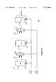
- FIG. 1illustrates the major functional blocks of the FPGA of the present invention
- FIG. 2illustrates one embodiment of the LE array of FIG. 1, and one embodiment of the enhanced LE;
- FIG. 3illustrates one embodiment each of the control logic and input selector for the master-slave latches of FIG. 1;
- FIGS. 4a-4billustrate one embodiment of the inter-LE crossbar network of FIG. 1
- FIG. 5illustrates one embodiment of the inter-FPGA crossbar network stage0 of FIG. 1;
- FIG. 6illustrates one embodiment of the associated read/write facilities of the context bus of FIG. 1;
- FIGS. 7a-7bare two exemplary timing diagrams illustrating the reading of a value from a LE and the writing of a value into a LE;
- FIG. 8illustrates one embodiment of the scan register of FIG. 1
- FIG. 9illustrates one embodiment of the trigger circuitry of FIG. 1.
- FPGA 100which is disposed on a single integrated circuit (or chip), comprises an array 102 of enhanced LEs incorporated with the teachings of the present invention.
- the enhanced LEsare used to "realize" various elements of circuit designs, however, as will be disclosed in more detail below, unlike the prior art, the enhanced LEs include new and innovative debugging features.
- FPGA 100further advantageously includes on-chip context bus 106, scan register 108 and trigger circuitry 110, coupled to the enhanced LEs as shown.
- context bus 106is used for inputting and outputting values to and from the LEs
- scan register 108 and trigger circuitry 110are used to output trace data and trigger inputs for FPGA 100 respectively.
- FPGA 100includes memory 112 to facilitate usage of FPGA 100 for emulating circuit designs with memory.
- memory 112is 16-bit wide.
- the pins 113 of FPGA 100can be used for either input or output.
- 64 I/O pins 113are provided to FPGA 100.
- FPGA 100also includes inter-LE crossbar (or x-bar) network 104 for interconnecting the LEs, memory 112, and I/O pins 113, as shown.
- FPGA 100it is also preferable for FPGA 100 to include "two copies" of the first stage of a crossbar network 114a-114b for inter-connecting FPGA 100 to other FPGAs and a "host system".
- Inter-LE crossbar network 104 and the first stage of inter-FPGA crossbar network 114a-114bare described in detail in copending application Ser. No. 08/542,519, now issued as U.S. Pat. No. 5,574,388, entitled "An emulation system employing a multi-level and multi-stage network topology for interconnecting reconfigurable logic devices", having common inventorship and assignee interest as the present invention, and filed contemporaneously with the present application, which is hereby fully incorporated by reference. Nevertheless, network 104 and network stages 114a-114b will be briefly described below. LEs, context bus 106, scan register 108, and trigger circuitry 110 will be described in further detail below with additional references to the remaining figures.
- FIG. 2illustrates one embodiment of the array of enhanced LEs of FIG. 1 and one embodiment of the LEs themselves in further detail.
- LE array 102comprises a plurality of enhanced LEs 200 of the present invention.
- LE array 102comprises 128 LEs 200.
- Each LE 200includes a multiple input--single output truth table 202, a pair of master-slave latches 204-206, output multiplexor 208, input multiplexor 212, and control logic 214, coupled to each other as shown.
- Truth table 202is used to generate a predetermined output in response to a set of inputs.
- truth-table 202has 4 inputs and 1 output. In other words, depending on the inputs, truth table 202 outputs 1 of 2 4 of predetermined outputs.
- Each of master-slave latches 204-206is used to store an input value synchronously with its clock input. Furthermore, each of master-slave latches 204-206 can be asynchronously forced to one or zero depending on the values of set and reset.
- the set and reset inputsare provided using the inputs 13 and 12 of truth table 202. In other words, if set/reset is used, the number of input variations that can be provided to truth-table 202 are reduced. Alternatively, additional dedicated pins may be provided to provide the set/reset signals to master-slave latches 204-206, however the real estate requirement of the FPGA will be increased.
- Output multiplexor 208, input multiplexor 210 and control logic 212are used to control the manner in which truth table 202 and master-slave latches 204-206 are used.
- Output multiplexor 208allows either the output of truth table 202 (by-passing master-slave latches 204-206) or the output of slave latch 206 (for level sensitive designs), or the output of master latch 204 (for edge sensitive designs) to be selected for output. The by-passed output is selected if truth table 202 is to be used standalone.
- input multiplexor 210allows either the output of truth table 202, the feedback from output multiplexor 208, or an input value on context bus 106 to be provided to master-slave latches 204-206.
- the feedback valueis selected to "freeze" LE 200, and the bus value is selected to initialize LE 200.
- Control logic 212controls input multiplexor 210 and the set and reset values provided to master-slave latches 204-206, in accordance to a set, a reset, a first and a second enable (ENAB and EN), a load (LDE) and a hold (HLD) value provided, to be described more fully below.
- Each LE 200also includes clock selection multiplexors 216a-216c for selectively providing a number of emulation clocks or a debug clock (LD) to master-slave latches 204-206.
- the emulation clocksinclude a "constructed" emulation clock using other LEs 200.
- this "constructed" emulation clockis made available through 10 of truth table 202.
- One of the emulation clocksis provided to master-slave latches 204-206 during normal operation, whereas the debug block (LD) is provided during debugging.
- the clock selectionis controlled by the CTX signal.
- LE 200also includes buffer 214a for outputting the selected output to inter-LE X-bar network 104 and the on-chip debugging facilities, and buffer 214b for outputting the selected output onto context bus 106 for direct observation outside FPGA 100.
- truth table 202may be used in a standalone manner, or in conjunction with the corresponding master-slave latches 204-206.
- Enhanced LE 200is suitable for "level sensitive” as well as “edge sensitive” circuit design emulations.
- each LE 200can be individually initialized.
- Each LE 200can also be caused to output the same output over and over again, as if it is frozen.
- LEs 200are individually and directly observable outside FPGA 100. In other words, there are no "hidden nodes”. The state of each "node” is directly observable outside the FPGA, without requiring the reconfiguration and time consuming re-compilation of circuit design mappings normally performed under the prior art.
- FIG. 3illustrates one embodiment each of input multiplexor 210 and control logic 212 in further detail.
- multiplexor 210comprises drivers 211a-211c for outputting the feedback output, the output of truth-table 202, and the input value on context bus 106 respectively, if enabled.
- One of drivers 211a-211cis selectively enabled by control signals from control logic 212.
- Control logic 212comprises AND gates 213a-213c, OR gate 215, NOR gate 217, and memory bits 219a-219c for generating the control signals for driver 211a-211c, as well as the set and reset values for master-slave latches 204-206.
- Memory bits 219a-219care used to store configuration information for enabling the provision of the set and reset values and the selection of the feedback output. If enabled, AND gates 213a-213b provides the set and reset values in accordance to the set and HLD inputs, and the reset and HLD inputs respectively. If enabled, OR gate 215 in conjunction with AND gate 213c provide the control signal for driver 211a in accordance to the ENAB, HLD and EN inputs. NOR gate 217 provide the control signal for driver 211b in accordance to the control signal being provided for driver 211a and a LDE input. Lastly, the LDE input is provided as the control signal for driver 211c.
- inter-LE crossbar network 104for interconnecting the LEs, the memory and the I/O pins is illustrated.
- inter-LE crossbar network 104comprises 4 subnetworks 220.
- the first two subnetworks, subnet0 and subnet1are used to route 72 signals, whereas the remaining two subnetworks, subnet2 and subnet3, are used to rout 64 signals.
- SubnetOis used to route the signals of LE0-LE39, LE119-LE127, I/O0-I/O15 and M0-M7.
- Subnet1is used to route the signals of LE24-LE71, I/O16-I/O31 and M8-M15.
- Subnet2is used to route the signals of LE56-LE103, and I/O32-I/O47.
- Subnet3is used to route the signals of LE0-LE7, LE88-LE127, and I/O48-I/O63. The overlapping coverage of the LEs provides increased flexibility of signal routing for mapping circuit designs.
- Each subnetwork 220is a three-stage Claus network comprising either 9 or 8 8-to-8 crossbars 222 in the first stage, 8 9-to-20 or 8-to-20 crossbars 224 or 226 in stage two, and 20 8-to-8 crossbars 228 in stage three.
- the stagesare coupled to each other in the well known "butterfly" manner.
- inter-LE crossbar network 104For further description of inter-LE crossbar network 104, refer to the incorporated by reference copending application Ser. No. 08/542,519 identified above.
- inter-FPGA crossbar network stage0 114a-114bfor interconnecting the FPGA to other FPGAs and a "host" computer is illustrated.
- inter-FPGA crossbar network stage0 114a-114bcomprises 4 pairs of 16-to-16 crossbars 230 for coupling 64 I/O signals of the FPGA to the next stage of a Claus network for interconnecting the FPGA to other FPGAs and a "host" computer.
- inter-FPGA crossbar network 114a-114balso refer to the incorporated by reference copending application Ser. No. 08/542,519 identified above.
- FIG. 6illustrates one embodiment of the read/write facilities associated with context bus 106 for reading from and writing into LEs 200 of FPGA 100.
- 128 LEs 200are organized in 16 columns, with each column having 8 LEs 200. Thus, all 128 LEs 200, or the current context, can be read or written with 16 8-bit words.
- Address register 232is provided for storing the read or write address.
- Decoder 234is provided for decoding the read or write address, which in conjunction with RAV control 236 provide the appropriate read control signals (RD0-RD15) and write control signals (LDE0-LDE15) for the 128 LEs 200.
- each LE 200receives the earlier described HLD signal for "freezing" the LEs 200, the CTX signal for selecting the debug (LD) clock, and the LD clock itself.
- FIGS. 7a-7billustrate exemplary signal timings for reading and writing.
- context readingis done by first loading a 4-bit address into address register 232.
- decoder 234causes RAN control 236 to drive the appropriate RD signals high to read out the contents of the addressed LEs 200. (HLD, CTX, LDEi and LD all remain low while a read operation is in progress.)
- context writingis done by first loading a 4-bit address into address register 232.
- HLDis first driven high to freeze all LEs 200.
- CTXis driven high to select debug clock LD for each LE 200.
- RNV control 236drives the appropriate LDE signals
- values on context bus 106are loaded into the addressed LEs 200. It is important to freeze all LEs 200 during a context writing, because partial context could induce temporary states, which could in turn put an emulation system into an unknown state. For example, the final context may drive a given RESET signal to the low state, but the partial context (during the writing operation) may induce a temporary high state on the RESET signal, thus unpredictably resetting all the latches connected to the signal.
- FIG. 8illustrates one embodiment of scan register 108 for outputting trace data.
- scan register 108comprises 16 sets of 8 flip-flops 242, and 15 sets of 8 multiplexors 244, disposed in between flip-flop sets 242.
- Flip-flop set0 242is coupled to a first group of 8 LEs 200.
- Multiplexor set0 244is coupled to flip-flop set0 242 and a second group of LEs 200.
- Flip-flop set1 242is coupled to multiplexor set0, and so forth.
- Flip-flop set0 242sequentially receives and propagates the outputs of the first group of 8 LEs 200.
- Multiplexor set0 242either serially provides the outputs of flip-flop set0 242 or the outputs of the second group of 8 LEs.
- Flip-flop set1 242in turn sequentially propagates the inputs it received from multiplexor set0 244.
- Flip-flop sets 242are controlled by a scan clock, whereas, multiplexor sets 244 are controlled by a scan control signal.
- a scan clock having the appropriate divided frequencyrelative to the operating emulation clock
- selectively applying the appropriate scan control signal to the multiplexor sets 244a snapshot of 128 LEs at a particular clock cycle can be sequentially scanned out of FPGA 100.
- FIG. 9illustrates one embodiment of trigger circuitry 110 for outputting trigger inputs.
- trigger circuitry 110comprises 4 comparator-register circuits 260 for generating 4 trigger inputs, one from each comparator-register circuit 260.
- Each comparator-register circuit 260includes a register 262 for storing a signal pattern, and an equality comparator 264 for comparing the outputs of the LEs to the stored content of pattern register 262.
- the signal patterncomprises 2-bits per LE 200, allowing the values of High, Low, or Don't Care to be encoded.
- An input to a trigger outside FPGA 100is generated whenever the stored pattern is detected.
- 4 LE internal state eventscan be monitored simultaneously.
Landscapes
- Physics & Mathematics (AREA)
- Mathematical Physics (AREA)
- Engineering & Computer Science (AREA)
- General Engineering & Computer Science (AREA)
- Computer Hardware Design (AREA)
- Computing Systems (AREA)
- General Physics & Mathematics (AREA)
- Computer Networks & Wireless Communication (AREA)
- Logic Circuits (AREA)
- Test And Diagnosis Of Digital Computers (AREA)
Abstract
Description
Claims (18)
Priority Applications (6)
| Application Number | Priority Date | Filing Date | Title |
|---|---|---|---|
| US08/542,838US5777489A (en) | 1995-10-13 | 1995-10-13 | Field programmable gate array with integrated debugging facilities |
| US08/985,372US6057706A (en) | 1995-10-13 | 1997-12-04 | Field programmable gate array with integrated debugging facilities |
| US09/404,925US6265894B1 (en) | 1995-10-13 | 1999-09-24 | Reconfigurable integrated circuit with integrated debugging facilities for use in an emulation system |
| US09/525,210US6388465B1 (en) | 1995-10-13 | 2000-03-14 | Reconfigurable integrated circuit with integrated debussing facilities and scalable programmable interconnect |
| US10/086,813US6717433B2 (en) | 1995-10-13 | 2002-02-28 | Reconfigurable integrated circuit with integrated debugging facilities and scalable programmable interconnect |
| US10/806,235US20040178820A1 (en) | 1995-10-13 | 2004-03-23 | Reconfigurable integrated circuit with integrated debugging facilities and scalable programmable interconnect |
Applications Claiming Priority (1)
| Application Number | Priority Date | Filing Date | Title |
|---|---|---|---|
| US08/542,838US5777489A (en) | 1995-10-13 | 1995-10-13 | Field programmable gate array with integrated debugging facilities |
Related Child Applications (1)
| Application Number | Title | Priority Date | Filing Date |
|---|---|---|---|
| US08/985,372ContinuationUS6057706A (en) | 1995-10-13 | 1997-12-04 | Field programmable gate array with integrated debugging facilities |
Publications (1)
| Publication Number | Publication Date |
|---|---|
| US5777489Atrue US5777489A (en) | 1998-07-07 |
Family
ID=24165499
Family Applications (5)
| Application Number | Title | Priority Date | Filing Date |
|---|---|---|---|
| US08/542,838Expired - LifetimeUS5777489A (en) | 1995-10-13 | 1995-10-13 | Field programmable gate array with integrated debugging facilities |
| US08/985,372Expired - LifetimeUS6057706A (en) | 1995-10-13 | 1997-12-04 | Field programmable gate array with integrated debugging facilities |
| US09/525,210Expired - LifetimeUS6388465B1 (en) | 1995-10-13 | 2000-03-14 | Reconfigurable integrated circuit with integrated debussing facilities and scalable programmable interconnect |
| US10/086,813Expired - LifetimeUS6717433B2 (en) | 1995-10-13 | 2002-02-28 | Reconfigurable integrated circuit with integrated debugging facilities and scalable programmable interconnect |
| US10/806,235AbandonedUS20040178820A1 (en) | 1995-10-13 | 2004-03-23 | Reconfigurable integrated circuit with integrated debugging facilities and scalable programmable interconnect |
Family Applications After (4)
| Application Number | Title | Priority Date | Filing Date |
|---|---|---|---|
| US08/985,372Expired - LifetimeUS6057706A (en) | 1995-10-13 | 1997-12-04 | Field programmable gate array with integrated debugging facilities |
| US09/525,210Expired - LifetimeUS6388465B1 (en) | 1995-10-13 | 2000-03-14 | Reconfigurable integrated circuit with integrated debussing facilities and scalable programmable interconnect |
| US10/086,813Expired - LifetimeUS6717433B2 (en) | 1995-10-13 | 2002-02-28 | Reconfigurable integrated circuit with integrated debugging facilities and scalable programmable interconnect |
| US10/806,235AbandonedUS20040178820A1 (en) | 1995-10-13 | 2004-03-23 | Reconfigurable integrated circuit with integrated debugging facilities and scalable programmable interconnect |
Country Status (1)
| Country | Link |
|---|---|
| US (5) | US5777489A (en) |
Cited By (57)
| Publication number | Priority date | Publication date | Assignee | Title |
|---|---|---|---|---|
| US5860008A (en)* | 1996-02-02 | 1999-01-12 | Apple Computer, Inc. | Method and apparatus for decompiling a compiled interpretive code |
| EP0898282A3 (en)* | 1997-07-23 | 1999-08-11 | Matsushita Electric Industrial Co., Ltd. | Semiconductor integrated circuit and method for designing the same |
| US6057706A (en)* | 1995-10-13 | 2000-05-02 | Mentor Graphics Corporation | Field programmable gate array with integrated debugging facilities |
| US6141636A (en)* | 1997-03-31 | 2000-10-31 | Quickturn Design Systems, Inc. | Logic analysis subsystem in a time-sliced emulator |
| WO2001024066A1 (en)* | 1999-09-24 | 2001-04-05 | Mentor Graphics Corporation | A regionally time multiplexed emulation system |
| US6242946B1 (en) | 1996-04-15 | 2001-06-05 | Altera Corporation | Embedded memory block with FIFO mode for programmable logic device |
| US6262933B1 (en) | 1999-01-29 | 2001-07-17 | Altera Corporation | High speed programmable address decoder |
| US6265894B1 (en)* | 1995-10-13 | 2001-07-24 | Frederic Reblewski | Reconfigurable integrated circuit with integrated debugging facilities for use in an emulation system |
| US6289494B1 (en) | 1997-11-12 | 2001-09-11 | Quickturn Design Systems, Inc. | Optimized emulation and prototyping architecture |
| US6294928B1 (en)* | 1996-04-05 | 2001-09-25 | Altera Corporation | Programmable logic device with highly routable interconnect |
| US20010047253A1 (en)* | 2000-03-02 | 2001-11-29 | Swoboda Gary L. | Data processing condition detector with table lookup |
| US6412104B1 (en)* | 1999-02-01 | 2002-06-25 | Taiwan Semiconductor Manufacturing Co., Ltd. | Integrated circuit debugging system |
| US6446249B1 (en) | 2000-05-11 | 2002-09-03 | Quickturn Design Systems, Inc. | Emulation circuit with a hold time algorithm, logic and analyzer and shadow memory |
| US20020144201A1 (en)* | 1999-08-30 | 2002-10-03 | Albrecht Mayer | Program-controlled unit and method for identifying and/or analyzing errors in program-controlled units |
| US6486702B1 (en) | 1999-07-02 | 2002-11-26 | Altera Corporation | Embedded memory blocks for programmable logic |
| US20020177990A1 (en)* | 1997-05-30 | 2002-11-28 | Sample Stephen P. | Distributed logic analyzer for use in a hardware logic emulation system |
| US6492834B1 (en) | 1996-04-05 | 2002-12-10 | Altera Corporation | Programmable logic device with highly routable interconnect |
| US6539535B2 (en) | 2000-05-11 | 2003-03-25 | Quickturn Design Systems, Inc. | Programmable logic device having integrated probing structures |
| US6570404B1 (en)* | 1996-03-29 | 2003-05-27 | Altera Corporation | High-performance programmable logic architecture |
| US6581191B1 (en) | 1999-11-30 | 2003-06-17 | Synplicity, Inc. | Hardware debugging in a hardware description language |
| US6604230B1 (en) | 1999-02-09 | 2003-08-05 | The Governing Counsel Of The University Of Toronto | Multi-logic device systems having partial crossbar and direct interconnection architectures |
| US20040025122A1 (en)* | 2000-11-28 | 2004-02-05 | Schubert Nils Endric | Hardware-based HDL code coverage and design analysis |
| US20040034841A1 (en)* | 2001-10-30 | 2004-02-19 | Frederic Reblewski | Emulation components and system including distributed event monitoring, and testing of an IC design under emulation |
| US6720796B1 (en) | 2001-05-06 | 2004-04-13 | Altera Corporation | Multiple size memories in a programmable logic device |
| US6762638B2 (en)* | 2002-10-16 | 2004-07-13 | International Business Machines Corporation | Circuit for preserving data in a flip-flop and a method of use |
| US20040148153A1 (en)* | 2003-01-23 | 2004-07-29 | Quickturn Design Systems, Inc. | Memory rewind and reconstruction for hardware emulator |
| US6823497B2 (en) | 1999-11-30 | 2004-11-23 | Synplicity, Inc. | Method and user interface for debugging an electronic system |
| US20040254778A1 (en)* | 2003-06-12 | 2004-12-16 | Mentor Graphics Corporation | Reconfigurable logic element with input swapping |
| US20040260530A1 (en)* | 2001-10-30 | 2004-12-23 | Frederic Josso | Distributed configuration of integrated circuits in an emulation system |
| US20040267489A1 (en)* | 2003-06-24 | 2004-12-30 | Frederic Reblewski | Data compaction and pin assignment |
| US20050010880A1 (en)* | 1999-11-30 | 2005-01-13 | Bridges2Silicon, Inc. | Method and user interface for debugging an electronic system |
| US20050027505A1 (en)* | 2003-08-01 | 2005-02-03 | Xavier Montagne | Configuration of reconfigurable interconnect portions |
| US20050071716A1 (en)* | 2003-09-30 | 2005-03-31 | Xavier Montagne | Testing of reconfigurable logic and interconnect sources |
| US20050068949A1 (en)* | 2003-09-30 | 2005-03-31 | Philippe Diehl | Message-based low latency circuit emulation signal transfer |
| US20050267732A1 (en)* | 2004-06-01 | 2005-12-01 | Quickturn Design Systems, Inc. | Method of visualization in processor based emulation system |
| US20050267728A1 (en)* | 2004-06-01 | 2005-12-01 | Quickturn Design Systems, Inc. | System and method for reliably supporting multiple signaling technologies |
| US20050267727A1 (en)* | 2004-06-01 | 2005-12-01 | Quickturn Design Systems, Inc. | System and method for providing flexible signal routing and timing |
| US20050267729A1 (en)* | 2004-06-01 | 2005-12-01 | Quickturn Design Systems, Inc. | Extensible memory architecture and communication protocol for supporting multiple devices in low-bandwidth, asynchronous applications |
| US20050271078A1 (en)* | 2004-06-01 | 2005-12-08 | Quayle Barton L | System and method for configuring communication systems |
| US20050278163A1 (en)* | 2004-06-01 | 2005-12-15 | Quickturn Design Systems, Inc. | System and method for resolving artifacts in differential signals |
| US7035787B2 (en) | 2001-10-30 | 2006-04-25 | Mentor Graphics Corporation | Emulation components and system including distributed routing and configuration of emulation resources |
| US7065481B2 (en) | 1999-11-30 | 2006-06-20 | Synplicity, Inc. | Method and system for debugging an electronic system using instrumentation circuitry and a logic analyzer |
| US7072818B1 (en) | 1999-11-30 | 2006-07-04 | Synplicity, Inc. | Method and system for debugging an electronic system |
| US7286976B2 (en) | 2003-06-10 | 2007-10-23 | Mentor Graphics (Holding) Ltd. | Emulation of circuits with in-circuit memory |
| US20070260951A1 (en)* | 2006-05-03 | 2007-11-08 | Texas Instruments Incorporated | Uncompromised standard input set-up time with improved enable input set-up time characteristics in a storage circuit |
| US20080082885A1 (en)* | 2006-09-28 | 2008-04-03 | Hynix Semiconductor Inc. | Test circuit for testing command signal at package level in semiconductor device |
| US7555424B2 (en) | 2006-03-16 | 2009-06-30 | Quickturn Design Systems, Inc. | Method and apparatus for rewinding emulated memory circuits |
| US20100057426A1 (en)* | 2004-04-15 | 2010-03-04 | Mentor Graphics Corporation | Logic Design Modeling and Interconnection |
| US8098181B2 (en) | 2010-04-28 | 2012-01-17 | Teradyne, Inc. | Attenuator circuit |
| US8099271B2 (en) | 1999-11-30 | 2012-01-17 | Synopsys, Inc. | Design instrumentation circuitry |
| US20120110525A1 (en)* | 2010-11-02 | 2012-05-03 | Global Unichip Corporation | Hybrid electronic design system and reconfigurable connection matrix thereof |
| US8502522B2 (en) | 2010-04-28 | 2013-08-06 | Teradyne, Inc. | Multi-level triggering circuit |
| US8531176B2 (en) | 2010-04-28 | 2013-09-10 | Teradyne, Inc. | Driving an electronic instrument |
| US8542005B2 (en) | 2010-04-28 | 2013-09-24 | Teradyne, Inc. | Connecting digital storage oscilloscopes |
| US8595683B1 (en) | 2012-04-12 | 2013-11-26 | Cadence Design Systems, Inc. | Generating user clocks for a prototyping environment |
| US20140372426A1 (en)* | 2013-06-12 | 2014-12-18 | International Business Machines Corporation | Filtering event log entries |
| US10303149B2 (en) | 2015-01-28 | 2019-05-28 | Mitsubishi Electric Corporation | Intelligent function unit and programmable logic controller system |
Families Citing this family (41)
| Publication number | Priority date | Publication date | Assignee | Title |
|---|---|---|---|---|
| US6370487B1 (en)* | 1998-04-23 | 2002-04-09 | Micron Technology, Inc. | Remote semiconductor microscopy |
| US20060117274A1 (en)* | 1998-08-31 | 2006-06-01 | Tseng Ping-Sheng | Behavior processor system and method |
| US6545549B2 (en)* | 2000-03-02 | 2003-04-08 | Texas Instruments Incorporated | Remotely controllable phase locked loop clock circuit |
| US6659504B2 (en)* | 2001-05-18 | 2003-12-09 | Delphi Technologies, Inc. | Steering column for a vehicle |
| WO2003038613A1 (en)* | 2001-10-30 | 2003-05-08 | Mentor Graphics Corporation | Emulating components and system including distributed emulation methods |
| US6703862B1 (en)* | 2002-09-24 | 2004-03-09 | Xilinx, Inc. | Efficient loadable registers in programmable logic devices |
| US7167025B1 (en) | 2004-02-14 | 2007-01-23 | Herman Schmit | Non-sequentially configurable IC |
| US7379861B2 (en)* | 2004-05-28 | 2008-05-27 | Quickturn Design Systems, Inc. | Dynamic programming of trigger conditions in hardware emulation systems |
| JP4555968B2 (en)* | 2005-01-19 | 2010-10-06 | 国立大学法人 千葉大学 | Semiconductor integrated circuit |
| US8000954B2 (en) | 2005-03-16 | 2011-08-16 | Gaterocket, Inc. | FPGA emulation system |
| US7375550B1 (en)* | 2005-07-15 | 2008-05-20 | Tabula, Inc. | Configurable IC with packet switch configuration network |
| US7443196B2 (en)* | 2005-07-15 | 2008-10-28 | Tabula, Inc. | Configuration network for a configurable IC |
| US7679401B1 (en) | 2005-12-01 | 2010-03-16 | Tabula, Inc. | User registers implemented with routing circuits in a configurable IC |
| US7538574B1 (en)* | 2005-12-05 | 2009-05-26 | Lattice Semiconductor Corporation | Transparent field reconfiguration for programmable logic devices |
| US20070139074A1 (en)* | 2005-12-19 | 2007-06-21 | M2000 | Configurable circuits with microcontrollers |
| US7263456B2 (en)* | 2006-01-10 | 2007-08-28 | M2000 | On circuit finalization of configuration data in a reconfigurable circuit |
| US7768301B2 (en)* | 2006-01-17 | 2010-08-03 | Abound Logic, S.A.S. | Reconfigurable integrated circuits with scalable architecture including a plurality of special function elements |
| US7475164B2 (en)* | 2006-02-28 | 2009-01-06 | International Business Machines Corporation | Apparatus, system, and method for automated device configuration and testing |
| JP2008123106A (en)* | 2006-11-09 | 2008-05-29 | Nec Electronics Corp | Microcomputer and debug method for microcomputer |
| CN101191819B (en)* | 2006-11-21 | 2012-05-23 | 国际商业机器公司 | FPGA, FPGA configuration, debugging system and method |
| US7514957B2 (en) | 2007-03-20 | 2009-04-07 | Tabula, Inc | Configurable IC having a routing fabric with storage elements |
| US7595655B2 (en) | 2007-06-27 | 2009-09-29 | Tabula, Inc. | Retrieving data from a configurable IC |
| US7579867B2 (en)* | 2007-06-27 | 2009-08-25 | Tabula Inc. | Restructuring data from a trace buffer of a configurable IC |
| US8069425B2 (en) | 2007-06-27 | 2011-11-29 | Tabula, Inc. | Translating a user design in a configurable IC for debugging the user design |
| US8412990B2 (en)* | 2007-06-27 | 2013-04-02 | Tabula, Inc. | Dynamically tracking data values in a configurable IC |
| US7839162B2 (en)* | 2007-06-27 | 2010-11-23 | Tabula, Inc. | Configurable IC with deskewing circuits |
| US7652498B2 (en) | 2007-06-27 | 2010-01-26 | Tabula, Inc. | Integrated circuit with delay selecting input selection circuitry |
| US7501855B2 (en) | 2007-06-27 | 2009-03-10 | Tabula, Inc | Transport network for a configurable IC |
| US8990651B2 (en)* | 2007-09-19 | 2015-03-24 | Tabula, Inc. | Integrated circuit (IC) with primary and secondary networks and device containing such an IC |
| WO2010016857A1 (en) | 2008-08-04 | 2010-02-11 | Tabula, Inc. | Trigger circuits and event counters for an ic |
| WO2010033263A1 (en) | 2008-09-17 | 2010-03-25 | Tabula, Inc. | Controllable storage elements for an ic |
| US8072234B2 (en) | 2009-09-21 | 2011-12-06 | Tabula, Inc. | Micro-granular delay testing of configurable ICs |
| US8269524B2 (en)* | 2010-04-27 | 2012-09-18 | Atmel Corporation | General purpose input/output pin mapping |
| US8650514B2 (en) | 2010-06-23 | 2014-02-11 | Tabula, Inc. | Rescaling |
| US8788987B2 (en) | 2010-06-23 | 2014-07-22 | Tabula, Inc. | Rescaling |
| US8941409B2 (en) | 2011-07-01 | 2015-01-27 | Tabula, Inc. | Configurable storage elements |
| US9148151B2 (en) | 2011-07-13 | 2015-09-29 | Altera Corporation | Configurable storage elements |
| US9203397B1 (en) | 2011-12-16 | 2015-12-01 | Altera Corporation | Delaying start of user design execution |
| US9000801B1 (en) | 2013-02-27 | 2015-04-07 | Tabula, Inc. | Implementation of related clocks |
| US9154137B2 (en) | 2013-07-04 | 2015-10-06 | Altera Corporation | Non-intrusive monitoring and control of integrated circuits |
| CN111352025B (en)* | 2020-03-13 | 2020-12-11 | 京微齐力(深圳)科技有限公司 | Method, system and equipment for verifying configuration controller in FPGA (field programmable Gate array) |
Citations (28)
| Publication number | Priority date | Publication date | Assignee | Title |
|---|---|---|---|---|
| US3106698A (en)* | 1958-04-25 | 1963-10-08 | Bell Telephone Labor Inc | Parallel data processing apparatus |
| US3287702A (en)* | 1962-12-04 | 1966-11-22 | Westinghouse Electric Corp | Computer control |
| US3287703A (en)* | 1962-12-04 | 1966-11-22 | Westinghouse Electric Corp | Computer |
| US3473160A (en)* | 1966-10-10 | 1969-10-14 | Stanford Research Inst | Electronically controlled microelectronic cellular logic array |
| US4020469A (en)* | 1975-04-09 | 1977-04-26 | Frank Manning | Programmable arrays |
| US4541071A (en)* | 1982-07-16 | 1985-09-10 | Nec Corporation | Dynamic gate array whereby an assembly of gates is simulated by logic operations on variables selected according to the gates |
| US4642487A (en)* | 1984-09-26 | 1987-02-10 | Xilinx, Inc. | Special interconnect for configurable logic array |
| US4669061A (en)* | 1984-12-21 | 1987-05-26 | Digital Equipment Corporation | Scannable flip-flop |
| US4700187A (en)* | 1985-12-02 | 1987-10-13 | Concurrent Logic, Inc. | Programmable, asynchronous logic cell and array |
| US4706216A (en)* | 1985-02-27 | 1987-11-10 | Xilinx, Inc. | Configurable logic element |
| US4722084A (en)* | 1985-10-02 | 1988-01-26 | Itt Corporation | Array reconfiguration apparatus and methods particularly adapted for use with very large scale integrated circuits |
| US4740919A (en)* | 1985-06-04 | 1988-04-26 | Texas Instruments Incorporated | Electrically programmable logic array |
| US4768196A (en)* | 1986-10-28 | 1988-08-30 | Silc Technologies, Inc. | Programmable logic array |
| US4786904A (en)* | 1986-12-15 | 1988-11-22 | Zoran Corporation | Electronically programmable gate array having programmable interconnect lines |
| US4791602A (en)* | 1983-04-14 | 1988-12-13 | Control Data Corporation | Soft programmable logic array |
| US4835705A (en)* | 1986-02-17 | 1989-05-30 | Mitsubishi Denki Kabushiki Kaisha | Interconnection area decision processor |
| US4849928A (en)* | 1987-01-28 | 1989-07-18 | Hauck Lane T | Logic array programmer |
| US4870302A (en)* | 1984-03-12 | 1989-09-26 | Xilinx, Inc. | Configurable electrical circuit having configurable logic elements and configurable interconnects |
| US4876466A (en)* | 1987-11-20 | 1989-10-24 | Mitsubishi Denki Kabushiki Kaisha | Programmable logic array having a changeable logic structure |
| US4918440A (en)* | 1986-11-07 | 1990-04-17 | Furtek Frederick C | Programmable logic cell and array |
| US4935734A (en)* | 1985-09-11 | 1990-06-19 | Pilkington Micro-Electronics Limited | Semi-conductor integrated circuits/systems |
| US4942577A (en)* | 1987-04-21 | 1990-07-17 | Nec Corporation | Logic circuit system with latch circuits for reliable scan-path testing |
| US4974226A (en)* | 1987-09-25 | 1990-11-27 | Mitsubishi Denki Kabushiki Kaisha | Circuit for testing integrated circuits |
| US5023775A (en)* | 1985-02-14 | 1991-06-11 | Intel Corporation | Software programmable logic array utilizing "and" and "or" gates |
| US5084874A (en)* | 1988-09-07 | 1992-01-28 | Texas Instruments Incorporated | Enhanced test circuit |
| US5450415A (en)* | 1992-11-25 | 1995-09-12 | Matsushita Electric Industrial Co., Ltd. | Boundary scan cell circuit and boundary scan test circuit |
| US5530706A (en)* | 1993-10-15 | 1996-06-25 | Hewlett-Packard Company | Non-destructive sampling of internal states while operating at normal frequency |
| US5553082A (en)* | 1995-05-01 | 1996-09-03 | International Business Machines Corporation | Built-in self-test for logic circuitry at memory array output |
Family Cites Families (23)
| Publication number | Priority date | Publication date | Assignee | Title |
|---|---|---|---|---|
| US3761695A (en) | 1972-10-16 | 1973-09-25 | Ibm | Method of level sensitive testing a functional logic system |
| USRE34363E (en) | 1984-03-12 | 1993-08-31 | Xilinx, Inc. | Configurable electrical circuit having configurable logic elements and configurable interconnects |
| US4602210A (en) | 1984-12-28 | 1986-07-22 | General Electric Company | Multiplexed-access scan testable integrated circuit |
| US4700178A (en)* | 1985-06-18 | 1987-10-13 | Kobishi Electric Co., Ltd. | A.C. alarm buzzer |
| US4635261A (en) | 1985-06-26 | 1987-01-06 | Motorola, Inc. | On chip test system for configurable gate arrays |
| US4758745B1 (en) | 1986-09-19 | 1994-11-15 | Actel Corp | User programmable integrated circuit interconnect architecture and test method |
| US5329471A (en) | 1987-06-02 | 1994-07-12 | Texas Instruments Incorporated | Emulation devices, systems and methods utilizing state machines |
| US4860290A (en) | 1987-06-02 | 1989-08-22 | Texas Instruments Incorporated | Logic circuit having individually testable logic modules |
| US4855669A (en)* | 1987-10-07 | 1989-08-08 | Xilinx, Inc. | System for scan testing of logic circuit networks |
| US5068603A (en) | 1987-10-07 | 1991-11-26 | Xilinx, Inc. | Structure and method for producing mask-programmed integrated circuits which are pin compatible substitutes for memory-configured logic arrays |
| EP0651343B1 (en) | 1988-10-05 | 2004-04-28 | Quickturn Design Systems, Inc. | Method of using electronically reconfigurable gate array logic and apparatus formed thereby |
| US5132974A (en) | 1989-10-24 | 1992-07-21 | Silc Technologies, Inc. | Method and apparatus for designing integrated circuits for testability |
| FR2660510A1 (en) | 1990-03-27 | 1991-10-04 | Dune Technologies | Method and device for programmable interconnection between two electronic circuit assemblies and application to a programmable logic circuit |
| US5321828A (en)* | 1991-06-07 | 1994-06-14 | Step Engineering | High speed microcomputer in-circuit emulator |
| US5425036A (en)* | 1992-09-18 | 1995-06-13 | Quickturn Design Systems, Inc. | Method and apparatus for debugging reconfigurable emulation systems |
| TW253942B (en) | 1994-01-31 | 1995-08-11 | At & T Corp | |
| US5680583A (en)* | 1994-02-16 | 1997-10-21 | Arkos Design, Inc. | Method and apparatus for a trace buffer in an emulation system |
| US5550843A (en) | 1994-04-01 | 1996-08-27 | Xilinx, Inc. | Programmable scan chain testing structure and method |
| US5633813A (en) | 1994-05-04 | 1997-05-27 | Srinivasan; Seshan R. | Apparatus and method for automatic test generation and fault simulation of electronic circuits, based on programmable logic circuits |
| US5574388A (en)* | 1995-10-13 | 1996-11-12 | Mentor Graphics Corporation | Emulation system having a scalable multi-level multi-stage programmable interconnect network |
| US5777489A (en)* | 1995-10-13 | 1998-07-07 | Mentor Graphics Corporation | Field programmable gate array with integrated debugging facilities |
| US5663813A (en)* | 1996-05-29 | 1997-09-02 | Primax Electronics, Ltd. | Image scanning device mounted to computer case |
| AUPP702498A0 (en)* | 1998-11-09 | 1998-12-03 | Silverbrook Research Pty Ltd | Image creation method and apparatus (ART77) |
- 1995
- 1995-10-13USUS08/542,838patent/US5777489A/ennot_activeExpired - Lifetime
- 1997
- 1997-12-04USUS08/985,372patent/US6057706A/ennot_activeExpired - Lifetime
- 2000
- 2000-03-14USUS09/525,210patent/US6388465B1/ennot_activeExpired - Lifetime
- 2002
- 2002-02-28USUS10/086,813patent/US6717433B2/ennot_activeExpired - Lifetime
- 2004
- 2004-03-23USUS10/806,235patent/US20040178820A1/ennot_activeAbandoned
Patent Citations (29)
| Publication number | Priority date | Publication date | Assignee | Title |
|---|---|---|---|---|
| US3106698A (en)* | 1958-04-25 | 1963-10-08 | Bell Telephone Labor Inc | Parallel data processing apparatus |
| US3287702A (en)* | 1962-12-04 | 1966-11-22 | Westinghouse Electric Corp | Computer control |
| US3287703A (en)* | 1962-12-04 | 1966-11-22 | Westinghouse Electric Corp | Computer |
| US3473160A (en)* | 1966-10-10 | 1969-10-14 | Stanford Research Inst | Electronically controlled microelectronic cellular logic array |
| US4020469A (en)* | 1975-04-09 | 1977-04-26 | Frank Manning | Programmable arrays |
| US4541071A (en)* | 1982-07-16 | 1985-09-10 | Nec Corporation | Dynamic gate array whereby an assembly of gates is simulated by logic operations on variables selected according to the gates |
| US4791602A (en)* | 1983-04-14 | 1988-12-13 | Control Data Corporation | Soft programmable logic array |
| US4870302A (en)* | 1984-03-12 | 1989-09-26 | Xilinx, Inc. | Configurable electrical circuit having configurable logic elements and configurable interconnects |
| US4642487A (en)* | 1984-09-26 | 1987-02-10 | Xilinx, Inc. | Special interconnect for configurable logic array |
| US4669061A (en)* | 1984-12-21 | 1987-05-26 | Digital Equipment Corporation | Scannable flip-flop |
| US5023775A (en)* | 1985-02-14 | 1991-06-11 | Intel Corporation | Software programmable logic array utilizing "and" and "or" gates |
| US4706216A (en)* | 1985-02-27 | 1987-11-10 | Xilinx, Inc. | Configurable logic element |
| US4758985A (en)* | 1985-02-27 | 1988-07-19 | Xilinx, Inc. | Microprocessor oriented configurable logic element |
| US4740919A (en)* | 1985-06-04 | 1988-04-26 | Texas Instruments Incorporated | Electrically programmable logic array |
| US4935734A (en)* | 1985-09-11 | 1990-06-19 | Pilkington Micro-Electronics Limited | Semi-conductor integrated circuits/systems |
| US4722084A (en)* | 1985-10-02 | 1988-01-26 | Itt Corporation | Array reconfiguration apparatus and methods particularly adapted for use with very large scale integrated circuits |
| US4700187A (en)* | 1985-12-02 | 1987-10-13 | Concurrent Logic, Inc. | Programmable, asynchronous logic cell and array |
| US4835705A (en)* | 1986-02-17 | 1989-05-30 | Mitsubishi Denki Kabushiki Kaisha | Interconnection area decision processor |
| US4768196A (en)* | 1986-10-28 | 1988-08-30 | Silc Technologies, Inc. | Programmable logic array |
| US4918440A (en)* | 1986-11-07 | 1990-04-17 | Furtek Frederick C | Programmable logic cell and array |
| US4786904A (en)* | 1986-12-15 | 1988-11-22 | Zoran Corporation | Electronically programmable gate array having programmable interconnect lines |
| US4849928A (en)* | 1987-01-28 | 1989-07-18 | Hauck Lane T | Logic array programmer |
| US4942577A (en)* | 1987-04-21 | 1990-07-17 | Nec Corporation | Logic circuit system with latch circuits for reliable scan-path testing |
| US4974226A (en)* | 1987-09-25 | 1990-11-27 | Mitsubishi Denki Kabushiki Kaisha | Circuit for testing integrated circuits |
| US4876466A (en)* | 1987-11-20 | 1989-10-24 | Mitsubishi Denki Kabushiki Kaisha | Programmable logic array having a changeable logic structure |
| US5084874A (en)* | 1988-09-07 | 1992-01-28 | Texas Instruments Incorporated | Enhanced test circuit |
| US5450415A (en)* | 1992-11-25 | 1995-09-12 | Matsushita Electric Industrial Co., Ltd. | Boundary scan cell circuit and boundary scan test circuit |
| US5530706A (en)* | 1993-10-15 | 1996-06-25 | Hewlett-Packard Company | Non-destructive sampling of internal states while operating at normal frequency |
| US5553082A (en)* | 1995-05-01 | 1996-09-03 | International Business Machines Corporation | Built-in self-test for logic circuitry at memory array output |
Non-Patent Citations (28)
| Title |
|---|
| "The Programmable Gate Array Design Handbook," First Edition, Xilinx, 1986, pp. 1-1 to 4-33. |
| Anderson, "Restructurable VLSI Program" Report No. ESD-TR-80-192 (DARPA Contract No. F19628-80-C-002), Mar. 31,1980. |
| Anderson, Restructurable VLSI Program Report No. ESD TR 80 192 (DARPA Contract No. F19628 80 C 002), Mar. 31,1980.* |
| Gentile et al, "Design of Switches for Self-Reconfiguring VLSI Array Structures," Microprocessing and Microprogramming, North-Holland, 1984, pp. 99-108. |
| Gentile et al, Design of Switches for Self Reconfiguring VLSI Array Structures, Microprocessing and Microprogramming , North Holland, 1984, pp. 99 108.* |
| Jump et al, "Microprogrammed Arrays," IEEE Transactions on Computers, vol. C-21, No. 9, Sep. 1972, pp. 974-984. |
| Jump et al, Microprogrammed Arrays, IEEE Transactions on Computers, vol. C 21, No. 9, Sep. 1972, pp. 974 984.* |
| Kautz et al, "Cellular Interconnection Arrays," IEEE Transactions On Computers, vol. C-17, No. 5, May 1968, pp. 443-451. |
| Kautz et al, Cellular Interconnection Arrays, IEEE Transactions On Computers, vol. C 17, No. 5, May 1968, pp. 443 451.* |
| Kautz, "Cellular Logic-in-Memory Arrays," IEEE Transactions On Computers, vol. C-18, No. 8, Aug. 1969, pp. 719-727. |
| Kautz, Cellular Logic in Memory Arrays, IEEE Transactions On Computers, vol. C 18, No. 8, Aug. 1969, pp. 719 727.* |
| Manning, "An Approach to Highly Integrated, Computer-Maintained Cellular Arrays", IEEE Transactions on Computers, vol. C-26, No. 6, Jun. 1977, pp. 536-552. |
| Manning, An Approach to Highly Integrated, Computer Maintained Cellular Arrays , IEEE Transactions on Computers, vol. C 26, No. 6, Jun. 1977, pp. 536 552.* |
| Manning, Automatic Test, Configuration, And Repair of Cellular Arrays, Doctoral Thesis MAC TR 151 (MIT), Jun. 1975.* |
| Manning, Automatic Test, Configuration, And Repair of Cellular Arrays, Doctoral Thesis MAC TR-151 (MIT), Jun. 1975. |
| Minnick, "Cutpoint Cellular Logic," IEEE Transactions On Electronic Computers, Dec. 1964, pp. 685-698. |
| Minnick, "Survey of MIcrocellular Research," Stanford Research Institute Project 5876 (Contract AF 19(628)-5828), Jul. 1966. |
| Minnick, Cutpoint Cellular Logic, IEEE Transactions On Electronic Computers, Dec. 1964, pp. 685 698.* |
| Minnick, Survey of MIcrocellular Research, Stanford Research Institute Project 5876 (Contract AF 19(628) 5828), Jul. 1966.* |
| Sami et al, "Reconfigurable Architectures for VLSI Processing Arrays," AFIPS Conference Proceedings, 1983 National Computer Conference, May 16-19, 1983, pp. 565-577. |
| Sami et al, Reconfigurable Architectures for VLSI Processing Arrays, AFIPS Conference Proceedings, 1983 National Computer Conference, May 16 19, 1983, pp. 565 577.* |
| Shoup, "Programmable Cellular Logic Arrays," Doctoral Thesis (Carnegie-Mellon University; DARPA Contract No. F44620-67-C-0058), Mar. 1970. |
| Shoup, Programmable Cellular Logic Arrays, Doctoral Thesis (Carnegie Mellon University; DARPA Contract No. F44620 67 C 0058), Mar. 1970.* |
| The Programmable Gate Array Design Handbook, First Edition, Xilinx, 1986, pp. 1 1 to 4 33.* |
| Wynn, "Designing With Logic Cell Arrays," ELECTRO/87 and Mini-Micro Northeast Conference Record, 1987. |
| Wynn, "In-Circuit Emulation for ASIC-Based Designs," VLSI Systems Design, Oct. 1986, pp. 38-45. |
| Wynn, Designing With Logic Cell Arrays, ELECTRO/87 and Mini Micro Northeast Conference Record, 1987.* |
| Wynn, In Circuit Emulation for ASIC Based Designs, VLSI Systems Design, Oct. 1986, pp. 38 45.* |
Cited By (103)
| Publication number | Priority date | Publication date | Assignee | Title |
|---|---|---|---|---|
| US6388465B1 (en)* | 1995-10-13 | 2002-05-14 | Jean Barbier | Reconfigurable integrated circuit with integrated debussing facilities and scalable programmable interconnect |
| US6265894B1 (en)* | 1995-10-13 | 2001-07-24 | Frederic Reblewski | Reconfigurable integrated circuit with integrated debugging facilities for use in an emulation system |
| US6057706A (en)* | 1995-10-13 | 2000-05-02 | Mentor Graphics Corporation | Field programmable gate array with integrated debugging facilities |
| US6717433B2 (en) | 1995-10-13 | 2004-04-06 | Jean Barbier | Reconfigurable integrated circuit with integrated debugging facilities and scalable programmable interconnect |
| US20040178820A1 (en)* | 1995-10-13 | 2004-09-16 | Jean Barbier | Reconfigurable integrated circuit with integrated debugging facilities and scalable programmable interconnect |
| US5860008A (en)* | 1996-02-02 | 1999-01-12 | Apple Computer, Inc. | Method and apparatus for decompiling a compiled interpretive code |
| US6570404B1 (en)* | 1996-03-29 | 2003-05-27 | Altera Corporation | High-performance programmable logic architecture |
| US6882176B1 (en)* | 1996-03-29 | 2005-04-19 | Altera Corporation | High-performance programmable logic architecture |
| US6294928B1 (en)* | 1996-04-05 | 2001-09-25 | Altera Corporation | Programmable logic device with highly routable interconnect |
| US6492834B1 (en) | 1996-04-05 | 2002-12-10 | Altera Corporation | Programmable logic device with highly routable interconnect |
| US6242946B1 (en) | 1996-04-15 | 2001-06-05 | Altera Corporation | Embedded memory block with FIFO mode for programmable logic device |
| US6141636A (en)* | 1997-03-31 | 2000-10-31 | Quickturn Design Systems, Inc. | Logic analysis subsystem in a time-sliced emulator |
| US20020177990A1 (en)* | 1997-05-30 | 2002-11-28 | Sample Stephen P. | Distributed logic analyzer for use in a hardware logic emulation system |
| US6205566B1 (en) | 1997-07-23 | 2001-03-20 | Matsushita Electric Industrial Co., Ltd. | Semiconductor integrated circuit, method for designing the same, and storage medium where design program for semiconductor integrated circuit is stored |
| EP0898282A3 (en)* | 1997-07-23 | 1999-08-11 | Matsushita Electric Industrial Co., Ltd. | Semiconductor integrated circuit and method for designing the same |
| US6289494B1 (en) | 1997-11-12 | 2001-09-11 | Quickturn Design Systems, Inc. | Optimized emulation and prototyping architecture |
| US6625793B2 (en) | 1997-11-12 | 2003-09-23 | Quickturn Design Systems, Inc. | Optimized emulation and prototyping architecture |
| US6262933B1 (en) | 1999-01-29 | 2001-07-17 | Altera Corporation | High speed programmable address decoder |
| US6459303B1 (en) | 1999-01-29 | 2002-10-01 | Altera Corporation | High speed programmable address decoder |
| US6412104B1 (en)* | 1999-02-01 | 2002-06-25 | Taiwan Semiconductor Manufacturing Co., Ltd. | Integrated circuit debugging system |
| US6604230B1 (en) | 1999-02-09 | 2003-08-05 | The Governing Counsel Of The University Of Toronto | Multi-logic device systems having partial crossbar and direct interconnection architectures |
| US6486702B1 (en) | 1999-07-02 | 2002-11-26 | Altera Corporation | Embedded memory blocks for programmable logic |
| US6593772B2 (en) | 1999-07-02 | 2003-07-15 | Altera Corporation | Embedded memory blocks for programmable logic |
| US20020144201A1 (en)* | 1999-08-30 | 2002-10-03 | Albrecht Mayer | Program-controlled unit and method for identifying and/or analyzing errors in program-controlled units |
| US7089468B2 (en)* | 1999-08-30 | 2006-08-08 | Infineon Technologies Ag | Program-controlled unit and method for identifying and/or analyzing errors in program-controlled units |
| US7098688B2 (en) | 1999-09-24 | 2006-08-29 | Mentor Graphics Corporation | Regionally time multiplexed emulation system |
| US6947882B1 (en) | 1999-09-24 | 2005-09-20 | Mentor Graphics Corporation | Regionally time multiplexed emulation system |
| CN1399724B (en)* | 1999-09-24 | 2010-04-28 | 明导公司 | Reconfigurable integrated circuit with integrated debugging function for use in emulation system |
| WO2001024066A1 (en)* | 1999-09-24 | 2001-04-05 | Mentor Graphics Corporation | A regionally time multiplexed emulation system |
| US20040075469A1 (en)* | 1999-09-24 | 2004-04-22 | Mentor Graphics Corp. | Regionally time multiplexed emulation system |
| US7069526B2 (en) | 1999-11-30 | 2006-06-27 | Synplicity, Inc. | Hardware debugging in a hardware description language |
| US7072818B1 (en) | 1999-11-30 | 2006-07-04 | Synplicity, Inc. | Method and system for debugging an electronic system |
| US8099271B2 (en) | 1999-11-30 | 2012-01-17 | Synopsys, Inc. | Design instrumentation circuitry |
| US7506286B2 (en) | 1999-11-30 | 2009-03-17 | Synopsys, Inc. | Method and system for debugging an electronic system |
| US7065481B2 (en) | 1999-11-30 | 2006-06-20 | Synplicity, Inc. | Method and system for debugging an electronic system using instrumentation circuitry and a logic analyzer |
| US7356786B2 (en) | 1999-11-30 | 2008-04-08 | Synplicity, Inc. | Method and user interface for debugging an electronic system |
| US6823497B2 (en) | 1999-11-30 | 2004-11-23 | Synplicity, Inc. | Method and user interface for debugging an electronic system |
| US20030182642A1 (en)* | 1999-11-30 | 2003-09-25 | Schubert Nils Endric | Hardware debugging in a hardware description language |
| US20050125754A1 (en)* | 1999-11-30 | 2005-06-09 | Schubert Nils E. | Hardware debugging in a hardware description language |
| US6581191B1 (en) | 1999-11-30 | 2003-06-17 | Synplicity, Inc. | Hardware debugging in a hardware description language |
| US20050010880A1 (en)* | 1999-11-30 | 2005-01-13 | Bridges2Silicon, Inc. | Method and user interface for debugging an electronic system |
| US20060195822A1 (en)* | 1999-11-30 | 2006-08-31 | Beardslee John M | Method and system for debugging an electronic system |
| US6904577B2 (en) | 1999-11-30 | 2005-06-07 | Synplicity, Inc. | Hardware debugging in a hardware description language |
| US7113902B2 (en)* | 2000-03-02 | 2006-09-26 | Texas Instruments Incorporated | Data processing condition detector with table lookup |
| US20060248396A1 (en)* | 2000-03-02 | 2006-11-02 | Swoboda Gary L | Data Processing Condition Detector With Table Lookup |
| US7761285B2 (en)* | 2000-03-02 | 2010-07-20 | Texas Instruments Incorporated | Data processing condition detector with table lookup |
| US20010047253A1 (en)* | 2000-03-02 | 2001-11-29 | Swoboda Gary L. | Data processing condition detector with table lookup |
| US6539535B2 (en) | 2000-05-11 | 2003-03-25 | Quickturn Design Systems, Inc. | Programmable logic device having integrated probing structures |
| US6446249B1 (en) | 2000-05-11 | 2002-09-03 | Quickturn Design Systems, Inc. | Emulation circuit with a hold time algorithm, logic and analyzer and shadow memory |
| US6697957B1 (en) | 2000-05-11 | 2004-02-24 | Quickturn Design Systems, Inc. | Emulation circuit with a hold time algorithm, logic analyzer and shadow memory |
| US7222315B2 (en) | 2000-11-28 | 2007-05-22 | Synplicity, Inc. | Hardware-based HDL code coverage and design analysis |
| US20040025122A1 (en)* | 2000-11-28 | 2004-02-05 | Schubert Nils Endric | Hardware-based HDL code coverage and design analysis |
| US20070198959A1 (en)* | 2000-11-28 | 2007-08-23 | Schubert Nils E | Hardware-based HDL code coverage and design analysis |
| US7836416B2 (en) | 2000-11-28 | 2010-11-16 | Synopsys, Inc. | Hardware-based HDL code coverage and design analysis |
| US6720796B1 (en) | 2001-05-06 | 2004-04-13 | Altera Corporation | Multiple size memories in a programmable logic device |
| US20040260530A1 (en)* | 2001-10-30 | 2004-12-23 | Frederic Josso | Distributed configuration of integrated circuits in an emulation system |
| US7035787B2 (en) | 2001-10-30 | 2006-04-25 | Mentor Graphics Corporation | Emulation components and system including distributed routing and configuration of emulation resources |
| US20040034841A1 (en)* | 2001-10-30 | 2004-02-19 | Frederic Reblewski | Emulation components and system including distributed event monitoring, and testing of an IC design under emulation |
| US7305633B2 (en)* | 2001-10-30 | 2007-12-04 | Mentor Graphics Corporation | Distributed configuration of integrated circuits in an emulation system |
| US7130788B2 (en)* | 2001-10-30 | 2006-10-31 | Mentor Graphics Corporation | Emulation components and system including distributed event monitoring, and testing of an IC design under emulation |
| US6762638B2 (en)* | 2002-10-16 | 2004-07-13 | International Business Machines Corporation | Circuit for preserving data in a flip-flop and a method of use |
| US7440884B2 (en) | 2003-01-23 | 2008-10-21 | Quickturn Design Systems, Inc. | Memory rewind and reconstruction for hardware emulator |
| US20040148153A1 (en)* | 2003-01-23 | 2004-07-29 | Quickturn Design Systems, Inc. | Memory rewind and reconstruction for hardware emulator |
| US7286976B2 (en) | 2003-06-10 | 2007-10-23 | Mentor Graphics (Holding) Ltd. | Emulation of circuits with in-circuit memory |
| US20040254778A1 (en)* | 2003-06-12 | 2004-12-16 | Mentor Graphics Corporation | Reconfigurable logic element with input swapping |
| US20040267489A1 (en)* | 2003-06-24 | 2004-12-30 | Frederic Reblewski | Data compaction and pin assignment |
| US8024170B2 (en)* | 2003-08-01 | 2011-09-20 | Mentor Graphics Corporation | Configuration of reconfigurable interconnect portions |
| US20100141297A1 (en)* | 2003-08-01 | 2010-06-10 | Mentor Graphics Corporation | Configuration of Reconfigurable Interconnect Portions |
| US20050027505A1 (en)* | 2003-08-01 | 2005-02-03 | Xavier Montagne | Configuration of reconfigurable interconnect portions |
| US7693703B2 (en) | 2003-08-01 | 2010-04-06 | Mentor Graphics Corporation | Configuration of reconfigurable interconnect portions |
| US7924845B2 (en) | 2003-09-30 | 2011-04-12 | Mentor Graphics Corporation | Message-based low latency circuit emulation signal transfer |
| US20050071716A1 (en)* | 2003-09-30 | 2005-03-31 | Xavier Montagne | Testing of reconfigurable logic and interconnect sources |
| US20050068949A1 (en)* | 2003-09-30 | 2005-03-31 | Philippe Diehl | Message-based low latency circuit emulation signal transfer |
| US7587649B2 (en) | 2003-09-30 | 2009-09-08 | Mentor Graphics Corporation | Testing of reconfigurable logic and interconnect sources |
| US20100057426A1 (en)* | 2004-04-15 | 2010-03-04 | Mentor Graphics Corporation | Logic Design Modeling and Interconnection |
| US8346530B2 (en)* | 2004-04-15 | 2013-01-01 | Mentor Graphics Corporation | Logic design modeling and interconnection |
| US20050267727A1 (en)* | 2004-06-01 | 2005-12-01 | Quickturn Design Systems, Inc. | System and method for providing flexible signal routing and timing |
| US20050271078A1 (en)* | 2004-06-01 | 2005-12-08 | Quayle Barton L | System and method for configuring communication systems |
| US7606697B2 (en) | 2004-06-01 | 2009-10-20 | Quickturn Design Systems, Inc. | System and method for resolving artifacts in differential signals |
| US20050267732A1 (en)* | 2004-06-01 | 2005-12-01 | Quickturn Design Systems, Inc. | Method of visualization in processor based emulation system |
| US20050267728A1 (en)* | 2004-06-01 | 2005-12-01 | Quickturn Design Systems, Inc. | System and method for reliably supporting multiple signaling technologies |
| US7440866B2 (en) | 2004-06-01 | 2008-10-21 | Quickturn Design Systems Inc. | System and method for validating an input/output voltage of a target system |
| US7721036B2 (en) | 2004-06-01 | 2010-05-18 | Quickturn Design Systems Inc. | System and method for providing flexible signal routing and timing |
| US7640155B2 (en) | 2004-06-01 | 2009-12-29 | Quickturn Design Systems, Inc. | Extensible memory architecture and communication protocol for supporting multiple devices in low-bandwidth, asynchronous applications |
| US7739093B2 (en) | 2004-06-01 | 2010-06-15 | Quickturn Design System, Inc. | Method of visualization in processor based emulation system |
| US7738398B2 (en) | 2004-06-01 | 2010-06-15 | Quickturn Design Systems, Inc. | System and method for configuring communication systems |
| US20050267729A1 (en)* | 2004-06-01 | 2005-12-01 | Quickturn Design Systems, Inc. | Extensible memory architecture and communication protocol for supporting multiple devices in low-bandwidth, asynchronous applications |
| US20050278163A1 (en)* | 2004-06-01 | 2005-12-15 | Quickturn Design Systems, Inc. | System and method for resolving artifacts in differential signals |
| US7555424B2 (en) | 2006-03-16 | 2009-06-30 | Quickturn Design Systems, Inc. | Method and apparatus for rewinding emulated memory circuits |
| US20070260951A1 (en)* | 2006-05-03 | 2007-11-08 | Texas Instruments Incorporated | Uncompromised standard input set-up time with improved enable input set-up time characteristics in a storage circuit |
| US20080082885A1 (en)* | 2006-09-28 | 2008-04-03 | Hynix Semiconductor Inc. | Test circuit for testing command signal at package level in semiconductor device |
| US7676711B2 (en)* | 2006-09-28 | 2010-03-09 | Hynix Semiconductor, Inc. | Test circuit for testing command signal at package level in semiconductor device |
| US8098181B2 (en) | 2010-04-28 | 2012-01-17 | Teradyne, Inc. | Attenuator circuit |
| US8502522B2 (en) | 2010-04-28 | 2013-08-06 | Teradyne, Inc. | Multi-level triggering circuit |
| US8531176B2 (en) | 2010-04-28 | 2013-09-10 | Teradyne, Inc. | Driving an electronic instrument |
| US8542005B2 (en) | 2010-04-28 | 2013-09-24 | Teradyne, Inc. | Connecting digital storage oscilloscopes |
| US20120110525A1 (en)* | 2010-11-02 | 2012-05-03 | Global Unichip Corporation | Hybrid electronic design system and reconfigurable connection matrix thereof |
| US8744832B2 (en)* | 2010-11-02 | 2014-06-03 | Global Unichip Corporation | Hybrid electronic design system and reconfigurable connection matrix thereof |
| US8595683B1 (en) | 2012-04-12 | 2013-11-26 | Cadence Design Systems, Inc. | Generating user clocks for a prototyping environment |
| US20140372426A1 (en)* | 2013-06-12 | 2014-12-18 | International Business Machines Corporation | Filtering event log entries |
| US9231595B2 (en)* | 2013-06-12 | 2016-01-05 | International Business Machines Corporation | Filtering event log entries |
| US9904608B2 (en) | 2013-06-12 | 2018-02-27 | International Business Machines Corporation | Filtering event log entries |
| US10303149B2 (en) | 2015-01-28 | 2019-05-28 | Mitsubishi Electric Corporation | Intelligent function unit and programmable logic controller system |
Also Published As
| Publication number | Publication date |
|---|---|
| US20040178820A1 (en) | 2004-09-16 |
| US6388465B1 (en) | 2002-05-14 |
| US6717433B2 (en) | 2004-04-06 |
| US20020089349A1 (en) | 2002-07-11 |
| US6057706A (en) | 2000-05-02 |
Similar Documents
| Publication | Publication Date | Title |
|---|---|---|
| US5777489A (en) | Field programmable gate array with integrated debugging facilities | |
| EP1133702B1 (en) | A reconfigurable integrated circuit with integrated debugging facilities for use in an emulation system | |
| US5352940A (en) | Ram convertible look-up table based macrocell for PLDs | |
| US6014334A (en) | Sample and load scheme for observability of internal nodes in a PLD | |
| US4860290A (en) | Logic circuit having individually testable logic modules | |
| KR100234649B1 (en) | Field programmable gate array and its test method | |
| US4669061A (en) | Scannable flip-flop | |
| US5173904A (en) | Logic circuits systems, and methods having individually testable logic modules | |
| KR100214239B1 (en) | Integrated logic circuit with partial scan pass circuit and partial scan path design method | |
| JP4361681B2 (en) | ASIC test circuit | |
| US5077740A (en) | Logic circuit having normal input/output data paths disabled when test data is transferred during macrocell testing | |
| US5023485A (en) | Method and circuitry for testing a programmable logic device | |
| US4720672A (en) | Testability system | |
| EP1118938B1 (en) | A field programmable gate array with integrated debugging facilities | |
| EP0347908B1 (en) | Test facilitating circuit of logic circuit | |
| US4802133A (en) | Logic circuit | |
| US4894800A (en) | Reconfigurable register bit-slice for self-test | |
| EP0776481A1 (en) | Addressable serial test system | |
| JPH0776782B2 (en) | Signature compression circuit | |
| KR960016139B1 (en) | Device for inputting 3 test data input (3TDI) with boundary scan structure to integrated circuit | |
| JPS63108747A (en) | Gate array integrated circuit | |
| KR910009084B1 (en) | Logic circuit | |
| KR960015560B1 (en) | Device for inputting 2TDI (2 test data input) of boundary scan structure into integrated circuit | |
| JPH03174634A (en) | semiconductor integrated circuit | |
| JPH026772A (en) | Integrated circuit |
Legal Events
| Date | Code | Title | Description |
|---|---|---|---|
| AS | Assignment | Owner name:MENTOR GRAPHICS CORPORATION, CALIFORNIA Free format text:ASSIGNMENT OF ASSIGNORS INTEREST;ASSIGNORS:BARBIER, JEAN;LEPAPE, OLIVIER;REBLEWSKI, FREDERIC;REEL/FRAME:008044/0014 Effective date:19960522 | |
| STCF | Information on status: patent grant | Free format text:PATENTED CASE | |
| CC | Certificate of correction | ||
| AS | Assignment | Owner name:MENTOR GRAPHICS CORPORATION, OREGON Free format text:ASSIGNMENT OF ASSIGNORS INTEREST;ASSIGNOR:META SYSTEMS, INC.;REEL/FRAME:010639/0975 Effective date:20000213 | |
| FPAY | Fee payment | Year of fee payment:4 | |
| REMI | Maintenance fee reminder mailed | ||
| AS | Assignment | Owner name:MENTOR GRAPHICS CORPORATION,OREGON Free format text:RETROACTIVE ASSIGNMENT AND QUITCLAIM;ASSIGNORS:META SYSTEMS SARL;BARBIER, JEAN;LEPAPE, OLIVIER;AND OTHERS;REEL/FRAME:016547/0979 Effective date:20050826 Owner name:MENTOR GRAPHICS (HOLDING) LTD.,OREGON Free format text:RETROACTIVE ASSIGNMENT AND QUITCLAIM;ASSIGNORS:META SYSTEMS SARL;BARBIER, JEAN;LEPAPE, OLIVIER;AND OTHERS;REEL/FRAME:016547/0979 Effective date:20050826 Owner name:MENTOR GRAPHICS (HOLDING) LTD., OREGON Free format text:RETROACTIVE ASSIGNMENT AND QUITCLAIM;ASSIGNORS:META SYSTEMS SARL;BARBIER, JEAN;LEPAPE, OLIVIER;AND OTHERS;REEL/FRAME:016547/0979 Effective date:20050826 Owner name:MENTOR GRAPHICS CORPORATION, OREGON Free format text:RETROACTIVE ASSIGNMENT AND QUITCLAIM;ASSIGNORS:META SYSTEMS SARL;BARBIER, JEAN;LEPAPE, OLIVIER;AND OTHERS;REEL/FRAME:016547/0979 Effective date:20050826 | |
| REMI | Maintenance fee reminder mailed | ||
| FPAY | Fee payment | Year of fee payment:8 | |
| SULP | Surcharge for late payment | Year of fee payment:7 | |
| FPAY | Fee payment | Year of fee payment:12 | |
| FEPP | Fee payment procedure | Free format text:PAYOR NUMBER ASSIGNED (ORIGINAL EVENT CODE: ASPN); ENTITY STATUS OF PATENT OWNER: LARGE ENTITY Free format text:PAYER NUMBER DE-ASSIGNED (ORIGINAL EVENT CODE: RMPN); ENTITY STATUS OF PATENT OWNER: LARGE ENTITY |