US5776540A - Process for manufacturing a praseodymium oxide- and manganese oxide-containing baseplate for use in field emission displays - Google Patents
Process for manufacturing a praseodymium oxide- and manganese oxide-containing baseplate for use in field emission displaysDownload PDFInfo
- Publication number
- US5776540A US5776540AUS08/777,797US77779796AUS5776540AUS 5776540 AUS5776540 AUS 5776540AUS 77779796 AUS77779796 AUS 77779796AUS 5776540 AUS5776540 AUS 5776540A
- Authority
- US
- United States
- Prior art keywords
- layer
- baseplate
- praseodymium
- manganese
- manganese oxide
- Prior art date
- Legal status (The legal status is an assumption and is not a legal conclusion. Google has not performed a legal analysis and makes no representation as to the accuracy of the status listed.)
- Expired - Lifetime
Links
Images
Classifications
- H—ELECTRICITY
- H01—ELECTRIC ELEMENTS
- H01J—ELECTRIC DISCHARGE TUBES OR DISCHARGE LAMPS
- H01J31/00—Cathode ray tubes; Electron beam tubes
- H01J31/08—Cathode ray tubes; Electron beam tubes having a screen on or from which an image or pattern is formed, picked up, converted, or stored
- H01J31/10—Image or pattern display tubes, i.e. having electrical input and optical output; Flying-spot tubes for scanning purposes
- H01J31/12—Image or pattern display tubes, i.e. having electrical input and optical output; Flying-spot tubes for scanning purposes with luminescent screen
- H01J31/15—Image or pattern display tubes, i.e. having electrical input and optical output; Flying-spot tubes for scanning purposes with luminescent screen with ray or beam selectively directed to luminescent anode segments
- H—ELECTRICITY
- H01—ELECTRIC ELEMENTS
- H01J—ELECTRIC DISCHARGE TUBES OR DISCHARGE LAMPS
- H01J3/00—Details of electron-optical or ion-optical arrangements or of ion traps common to two or more basic types of discharge tubes or lamps
- H01J3/02—Electron guns
- H01J3/021—Electron guns using a field emission, photo emission, or secondary emission electron source
- H01J3/022—Electron guns using a field emission, photo emission, or secondary emission electron source with microengineered cathode, e.g. Spindt-type
- H—ELECTRICITY
- H01—ELECTRIC ELEMENTS
- H01J—ELECTRIC DISCHARGE TUBES OR DISCHARGE LAMPS
- H01J29/00—Details of cathode-ray tubes or of electron-beam tubes of the types covered by group H01J31/00
- H01J29/86—Vessels; Containers; Vacuum locks
- H01J29/863—Vessels or containers characterised by the material thereof
- H—ELECTRICITY
- H01—ELECTRIC ELEMENTS
- H01J—ELECTRIC DISCHARGE TUBES OR DISCHARGE LAMPS
- H01J2329/00—Electron emission display panels, e.g. field emission display panels
Definitions
- This inventionrelates generally to field emission displays and, more particularly, to a conductive, light-absorbing praseodymium-manganese oxide layer deposited on the surface of a baseplate within a field emission display to bleed off surface charge and absorb stray electrons.
- the cathode ray tubehas been used to perform this function.
- the CRTconsists of a scanning electron gun directed toward a phosphor-coated screen.
- the electron gunemits a stream of electrons that impinge upon individual phosphor picture elements or pixels on the screen.
- the electron gunemits a stream of electrons that impinge upon individual phosphor picture elements or pixels on the screen.
- the electronsstrike the pixels, they cause the energy level of the phosphor to increase.
- the pixelsemit photons. These photons pass through the screen to be seen by a viewer as a point of light.
- the CRThowever, has a number of disadvantages. In order to scan the entire width of the screen, the CRT screen must be relatively distant from the electron gun. This makes the entire unit large and bulky.
- the CRTalso requires a significant amount of power to operate.
- the field emission displayutilizes a baseplate of cold cathode emitter tips as a source of electrons in place of the scanning electron gun used in the CRT. When placed in an electric field, these emitter tips emit a stream of electrons in the direction of a faceplate to which phosphor pixels are adhered. Instead of a single gun firing electrons at the pixels, the FED has an array of emitter tips. Each of the emitter tips are individually addressable, and one or more of the emitter tips correspond to a single phosphor pixel on the faceplate.
- One of the problems associated with an FEDis that not all of the photons that are released from the pixels pass through the faceplate to be seen by the viewer as points of light. Rather, nearly half of the photons will proceed in the general direction of the baseplate, and may impinge upon the emitter tips and/or circuitry within the FED. This may cause an undesirable photoelectric effect, and any reflected light from the baseplate reduces the contrast of the FED.
- a further problemis that not all of the electrons released by the emitter tips actually excite their targeted pixel. Instead, some of these electrons are reflected internally, and may excite a non-targeted pixel.
- this inventionis generally directed to a conductive, light absorbing praseodymium-manganese oxide layer coated on the interior surface of an FED baseplate.
- the praseodymium-manganese oxide layerreduces the photoelectric effect and damage associated by reflected electrons from the faceplate, and improves display image and contrast due to absorption of any ambient light reaching the baseplate and/or by absorption of any photons emitted in the direction of the baseplate.
- a conductive and light-absorbing baseplatefor use in a field emission display. At least a portion of the interior surface of the baseplate (i.e., the surface opposite the faceplate) is coated with a praseodymium-manganese oxide layer having a resistivity which does not exceed 1 ⁇ 10 5 ⁇ ⁇ cm, preferably does not exceed 1 ⁇ 10 4 ⁇ ⁇ cm, and more preferably does not exceed 1 ⁇ 10 3 ⁇ ⁇ cm.
- the praseodymium-manganese oxide layeris coated on the baseplate at a thickness ranging from 1,000 ⁇ to 15,000 ⁇ , and has a light absorption coefficient of at least 1 ⁇ 10 5 cm -1 at a wavelength of 500 nm.
- an FEDwhich contains the conductive and light-absorbing baseplate of this invention.
- Such displaysare particularly suited for use in products which are employed under high ambient light conditions, including, but not limited to, the screen of a laptop computer.
- a process for manufacturing a conductive and light-absorbing baseplateincludes coating the interior surface of the baseplate with a layer of praseodymium-manganese oxide having a resistivity which does not exceed 1 ⁇ 10 5 ⁇ ⁇ cm.
- Suitable coating techniquesinclude (but are not limited to) deposition by RF sputtering.
- a process for manufacturing a conductive and light-absorbing praseodymium-manganese oxide materialincludes heating a mixture of a praseodymium compound and a manganese compound at a temperature ranging from 1200°-1500° C. for a period of time sufficient to yield the praseodymium-manganese oxide material.
- the praseodymium compoundis Pr 6 O 11 and the manganese compound is selected from MnO 2 and Mn(CO 3 ) 2 .
- the ratio of praseodymium to manganese within the praseodymium-manganese oxide materialis such that the material has a resistivity, after coating a layer of the same on the baseplate, that does not exceed 1 ⁇ 10 5 ⁇ ⁇ cm.
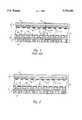
- FIG. 1is a cross-sectional view of a prior art field emission display screen, and illustrates both emitted and back-emitted photons, as well as internally-reflected electrons.
- FIG. 2is a cross-sectional view of a representative field emission display of this invention.
- the present inventionis directed to a conductive, light absorbing praseodymium-manganese oxide layer for use within an FED.
- This layerserves to bleed off surface charge associated with stray electrons within the FED, and must have a resistivity no greater than 1 ⁇ 10 5 ⁇ ⁇ cm, preferably no greater than 1 ⁇ 10 4 ⁇ ⁇ cm, and more preferably no greater than 1 ⁇ 10 3 ⁇ ⁇ cm.
- the praseodymium-manganese oxide layeralso serves to absorb back-emitted photons (i.e., photons emitted from the faceplate in the direction of the baseplate).
- the praseodymium-manganese oxide layerreadily absorbs light (i.e., the light absorption coefficient of praseodymium-manganese oxide is on the order of 1 ⁇ 10 5 cm -1 ), which provides a number of benefits to the FED.
- One of these benefitsis that it minimizes the photoelectric effect in the underlying circuitry due to stray photons striking the baseplate of the FED.
- a further beneficial propertyis that it provides better contrast between the emitted light and the ambient background reflection from the cathode surface.
- FIG. 1is a cross-sectional view of an FED screen 2 which is comprised of baseplate 3 and faceplate 4.
- Faceplate 4includes an array of pixels 6 in contact with conductive layer 9, which in turn is in contact with a transparent material 5.
- Baseplate 3includes an array of emitter tips 10 which protrude from a silicon substrate 12.
- a conductive layer 14contacts the emitter tips to an addressing scheme (not shown) that selectively connects each of the emitter tips to a power supply (not shown).
- An insulating layer 16surrounds each of the emitter tips 10.
- a conductive gate 18also surrounds the emitter tips and is separated from conductive layer 14 and substrate 12 by insulating layer 16.
- Conductive grid 18is connected to the positive terminal of a power supply through a similar addressing scheme (not shown) as that of the emitter tips.
- a similar addressing scheme(not shown) as that of the emitter tips.
- an electric fieldis placed between the appropriate conductive gate and emitter tip. This electric field causes emitter tip 11 to release a stream of electrons, represented by arrows 17 and 19, toward pixel 7 located on faceplate 4.
- FIG. 1depicts a single pixel corresponding to each emitter tip. However, it should be recognized that more than one emitter tip may be associated with a single pixel. Furthermore, the distance between faceplate 4 and baseplate 3 may be fixed by use of suitable supporting elements (not shown), and faceplate 4 and baseplate 3 are sealed along their edges and a high vacuum, for example, 1 ⁇ 10 -5 to 1 ⁇ 10 -8 torr, is maintained therein.
- photon 8is seen by the viewer as a point of light. However, it is equally likely that the photon will be released back toward baseplate 3, as represented by photon 15. In this instance, photon 15 may create a photoelectric effect which leads to undesirable electrons and holes in the components of baseplate 3.
- FIG. 1also illustrates a further problem associated with existing FED screens. Rather than exciting the phosphor pixel causing release of photons, electrons directed to a targeted pixel may be reflected, scattered or absorbed by the pixel. Some of these reflected electrons (as depicted by arrow 13 of FIG. 1) and/or those produced by secondary emissions may travel back in the direction of baseplate 3, again resulting in unwanted electrons and producing holes in baseplate 3.
- an FED screen 20 of this inventioncontains faceplate 4 and baseplate 3.
- a praseodymium-manganese oxide layer 22is in contact with conducting gate 18 which, in turn, is in contact with insulating layer 16 on conductive layer 14 and substrate 12.
- Emitter tips 10 and faceplate 4are the same as described above for FIG. 1.
- the praseodymium-manganese oxide layer 22is electrically isolated from the conductivity gate 18, for example, by an intermediate insulative layer (not shown), the praseodymium-manganese oxide layer 22 could be grounded. In any event, the praseodymium-manganese oxide layer sharply reduces the number of electrons that impinge on components of baseplate 3, thus eliminating undesirable electron holes therein.
- a praseodymium-manganese oxide materialwhich is suitable for depositing upon the interior surface of a baseplate of an FED.
- the praseodymium-manganese oxide materialmay be represented by the formula Pr:Mn:O 3 , wherein the molar ratio of praseodymium to manganese (Pr:Mn) may generally range from 0.1:1 to 1:0.1, and preferably from 0.5:1 to 1:0.5. This molar ratio has been found to yield suitable conductivity for the resulting praseodymium-manganese oxide layer. Furthermore, by increasing the amount of manganese in relation to praseodymium, conductivity is increased (i.e., resistivity is decreased).
- the praseodymium-manganese oxide materialmay be made by combining Pr 6 O 11 with MnO 2 or MnCO 3 in a mill jar, and milling the same to a powder containing particles having an average diameter of approximately 2 ⁇ m. This powder is then heated at a temperature ranging from 1200°-1500° C., preferably from 1250°-1430° C., for about 4 hours. After heating, the resulting material is very dark colored, essentially matte black. The heated material may then be re-crushed and milled to again yield a powder having an average particle diameter of about 2 ⁇ m.
- the ratio of Pr to Mninfluences the conductivity of the resulting praseodymium-manganese oxide layer.
- Such a ratiomay be controlled by the relative amounts of the components Pr 6 O 11 and MnO 2 or MnCO 3 .
- these componentsare mixed in amounts sufficient to yield the Pr:Mn ratio disclosed above.
- the praseodymium-manganese oxide materialmay be deposited on the interior surface of the baseplate by any number of techniques to a thickness ranging from 1,000 ⁇ to 15,000 ⁇ .
- deposition techniquesinclude, but are not limited to, radio frequency (RF) sputtering, laser ablation, plasma deposition, chemical vapor deposition (CVD) and electron beam evaporation.
- RFradio frequency
- CVDchemical vapor deposition
- electron beam evaporationelectron beam evaporation.
- the praseodymium-manganese oxide materialis compressed to make a planar target, which is then mounted within a suitable backing plate for RF sputtering.
- Sputteringmay then be carried out in an RF sputterer using argon or argon and oxygen gas, with a substrate temperature of 200°-350° C. and a sputtering pressure of about 6 ⁇ 10 -3 to about 3 ⁇ 10 -2 torr.
- organometallic precursors for Pr and Mnwould be employed, such as Pr acetate, Pr oxalate or Pr(Thd) 3 , as well as Mn acetate, Mn carbonyl, Mn methoxide and Mn oxalate.
- the resistivity of the praseodymium-manganese oxide materialmay also be controlled by, for example, firing the material (after deposited as a layer on the interior surface of the baseplate, in a reducing atmosphere, such as hydrogen and/or carbon monoxide. Such treatment serves to increase conductivity, or in other words, reduce resistivity to levels suitable for use in the practice of this invention.
- a reducing atmospheresuch as hydrogen and/or carbon monoxide.
- additional componentsmay be added to the material, such as conductive ions and/or metals, to further enhance conductivity.
- the resulting praseodymium-manganese oxide layer on the interior surface of the baseplateshields the underlying circuitry from photons and stray electrons as discussed above. Since the praseodymium-manganese oxide layer is very dark colored, it also yields high contrast to the FED. Furthermore, an FED which employs the present invention possess high legibility under ambient lighting conditions, and are particularly suited for use as screens for televisions, portable computers and as displays for outdoor use, such as avionics and automobiles.
- Pr 6 O 11 and MnO 2were purchase from a commercial source (Cerac, La Puente, Calif.) and used without further purification. Both components were placed in a mill jar (510.72 grams Pr 6 O 11 and 86.94 grams MnO 2 ), 500 ml of isopropyl alcohol was added, and the resulting slurry milled for 24 hours at 100 rpm. The slurry was dried in an oven under a nitrogen atmosphere. The dried material was fired at 1350° C. for 4 hours, and then cooled. The cooled material was ground to small particles (average diameter of about 2 ⁇ m) using a suitable grinding technique.
- the resulting powdered material of Example 1may be deposited on the baseplate by any of a variety of acceptable techniques.
- the powdered materialmay be sintered to form a planar sputter target.
- Sputteringmay then be carried out in an RF sputterer using argon or argon and oxygen gas, with a substrate temperature of 200°-350° C., and a pressure of about 6 ⁇ 10 -3 to 3 ⁇ 10 -2 torr.
- the baseplate of Example 2may used in the manufacture an FED screen using known techniques.
- the resulting FEDhas a number of advantages over existing products, including: reduced photoelectric effect; reduced damage by reflected electrons from the faceplate to the baseplate components; and improved display image and contrast due to absorption of any ambient light reaching the baseplate and/or by absorption of any photons emitted by the faceplate in the direction of the baseplate.
Landscapes
- Cathode-Ray Tubes And Fluorescent Screens For Display (AREA)
- Vessels, Lead-In Wires, Accessory Apparatuses For Cathode-Ray Tubes (AREA)
Abstract
Description
Claims (23)
Priority Applications (9)
| Application Number | Priority Date | Filing Date | Title |
|---|---|---|---|
| US08/777,797US5776540A (en) | 1996-05-14 | 1996-12-31 | Process for manufacturing a praseodymium oxide- and manganese oxide-containing baseplate for use in field emission displays |
| EP97926529AEP0898782B1 (en) | 1996-05-14 | 1997-05-14 | Field emission displays with praseodymium-manganese oxide layer |
| KR10-1998-0709298AKR100439455B1 (en) | 1996-05-14 | 1997-05-14 | Conductive, light-absorbing base plate and its manufacturing method, field emission display and conductive, light-absorbing praseodymium-manganese oxide layer manufacturing method |
| JP54112497AJP3799482B2 (en) | 1996-05-14 | 1997-05-14 | Rare earth metal-manganese oxide layers for field emission displays |
| DE69723433TDE69723433T2 (en) | 1996-05-14 | 1997-05-14 | FIELD EMISSION DISPLAY DEVICES WITH PRASEODYM MANGANE OXIDE LAYER |
| AU31273/97AAU3127397A (en) | 1996-05-14 | 1997-05-14 | Praseodymium-manganese oxide layer for use in field emission displays |
| PCT/US1997/008257WO1997043781A2 (en) | 1996-05-14 | 1997-05-14 | Praseodymium-manganese oxide layer for use in field emission displays |
| AT97926529TATE244928T1 (en) | 1996-05-14 | 1997-05-14 | FIELD EMISSION DEVICES WITH PRASEODYMUM MANGANEOUS OXIDE LAYER |
| US08/899,844US6413577B1 (en) | 1996-05-14 | 1997-07-24 | Process for operating a field emission display with a layer of praseodymium-manganese oxide material |
Applications Claiming Priority (2)
| Application Number | Priority Date | Filing Date | Title |
|---|---|---|---|
| US08/645,615US5668437A (en) | 1996-05-14 | 1996-05-14 | Praseodymium-manganese oxide layer for use in field emission displays |
| US08/777,797US5776540A (en) | 1996-05-14 | 1996-12-31 | Process for manufacturing a praseodymium oxide- and manganese oxide-containing baseplate for use in field emission displays |
Related Parent Applications (1)
| Application Number | Title | Priority Date | Filing Date |
|---|---|---|---|
| US08/645,615DivisionUS5668437A (en) | 1996-05-14 | 1996-05-14 | Praseodymium-manganese oxide layer for use in field emission displays |
Related Child Applications (1)
| Application Number | Title | Priority Date | Filing Date |
|---|---|---|---|
| US08/899,844DivisionUS6413577B1 (en) | 1996-05-14 | 1997-07-24 | Process for operating a field emission display with a layer of praseodymium-manganese oxide material |
Publications (1)
| Publication Number | Publication Date |
|---|---|
| US5776540Atrue US5776540A (en) | 1998-07-07 |
Family
ID=24589743
Family Applications (4)
| Application Number | Title | Priority Date | Filing Date |
|---|---|---|---|
| US08/645,615Expired - LifetimeUS5668437A (en) | 1996-05-14 | 1996-05-14 | Praseodymium-manganese oxide layer for use in field emission displays |
| US08/777,797Expired - LifetimeUS5776540A (en) | 1996-05-14 | 1996-12-31 | Process for manufacturing a praseodymium oxide- and manganese oxide-containing baseplate for use in field emission displays |
| US08/840,084Expired - LifetimeUS5759446A (en) | 1996-05-14 | 1997-04-09 | Process for preparing a praseodymium-manganese oxide material for use in field emission displays |
| US08/899,844Expired - Fee RelatedUS6413577B1 (en) | 1996-05-14 | 1997-07-24 | Process for operating a field emission display with a layer of praseodymium-manganese oxide material |
Family Applications Before (1)
| Application Number | Title | Priority Date | Filing Date |
|---|---|---|---|
| US08/645,615Expired - LifetimeUS5668437A (en) | 1996-05-14 | 1996-05-14 | Praseodymium-manganese oxide layer for use in field emission displays |
Family Applications After (2)
| Application Number | Title | Priority Date | Filing Date |
|---|---|---|---|
| US08/840,084Expired - LifetimeUS5759446A (en) | 1996-05-14 | 1997-04-09 | Process for preparing a praseodymium-manganese oxide material for use in field emission displays |
| US08/899,844Expired - Fee RelatedUS6413577B1 (en) | 1996-05-14 | 1997-07-24 | Process for operating a field emission display with a layer of praseodymium-manganese oxide material |
Country Status (2)
| Country | Link |
|---|---|
| US (4) | US5668437A (en) |
| KR (1) | KR100439455B1 (en) |
Cited By (5)
| Publication number | Priority date | Publication date | Assignee | Title |
|---|---|---|---|---|
| US6236157B1 (en) | 1999-02-26 | 2001-05-22 | Candescent Technologies Corporation | Tailored spacer structure coating |
| US6373174B1 (en) | 1999-12-10 | 2002-04-16 | Motorola, Inc. | Field emission device having a surface passivation layer |
| US20040027050A1 (en)* | 1999-06-25 | 2004-02-12 | Micron Display Technology, Inc. | Black matrix for flat panel field emission displays |
| US20050253059A1 (en)* | 2004-05-13 | 2005-11-17 | Goeringer Douglas E | Tandem-in-time and-in-space mass spectrometer and associated method for tandem mass spectrometry |
| US20070216306A1 (en)* | 2006-03-20 | 2007-09-20 | Chul-Hong Kim | Plasma display panel |
Families Citing this family (6)
| Publication number | Priority date | Publication date | Assignee | Title |
|---|---|---|---|---|
| US20010045794A1 (en)* | 1996-01-19 | 2001-11-29 | Alwan James J. | Cap layer on glass panels for improving tip uniformity in cold cathode field emission technology |
| US5719406A (en)* | 1996-10-08 | 1998-02-17 | Motorola, Inc. | Field emission device having a charge bleed-off barrier |
| US6144351A (en)* | 1997-02-19 | 2000-11-07 | Micron Technology, Inc. | Field emitter display baseplate and method of fabricating same |
| US5903100A (en)* | 1997-03-07 | 1999-05-11 | Industrial Technology Research Institute | Reduction of smearing in cold cathode displays |
| US20040170761A1 (en)* | 2003-02-27 | 2004-09-02 | Sharp Laboratories Of America, Inc. | Precursor solution and method for controlling the composition of MOCVD deposited PCMO |
| JP4843259B2 (en)* | 2005-06-10 | 2011-12-21 | シャープ株式会社 | Method for manufacturing variable resistance element |
Citations (10)
| Publication number | Priority date | Publication date | Assignee | Title |
|---|---|---|---|---|
| US3935119A (en)* | 1971-11-30 | 1976-01-27 | Owens-Illinois, Inc. | Luminescent device, process, composition, and article |
| US5129850A (en)* | 1991-08-20 | 1992-07-14 | Motorola, Inc. | Method of making a molded field emission electron emitter employing a diamond coating |
| US5201992A (en)* | 1990-07-12 | 1993-04-13 | Bell Communications Research, Inc. | Method for making tapered microminiature silicon structures |
| US5319279A (en)* | 1991-03-13 | 1994-06-07 | Sony Corporation | Array of field emission cathodes |
| US5455489A (en)* | 1994-04-11 | 1995-10-03 | Bhargava; Rameshwar N. | Displays comprising doped nanocrystal phosphors |
| US5528102A (en)* | 1994-05-24 | 1996-06-18 | Texas Instruments Incorporated | Anode plate with opaque insulating material for use in a field emission display |
| US5534749A (en)* | 1993-07-21 | 1996-07-09 | Sony Corporation | Field-emission display with black insulating layer between transparent electrode and conductive layer |
| US5585301A (en)* | 1995-07-14 | 1996-12-17 | Micron Display Technology, Inc. | Method for forming high resistance resistors for limiting cathode current in field emission displays |
| US5601751A (en)* | 1995-06-08 | 1997-02-11 | Micron Display Technology, Inc. | Manufacturing process for high-purity phosphors having utility in field emission displays |
| US5616061A (en)* | 1995-07-05 | 1997-04-01 | Advanced Vision Technologies, Inc. | Fabrication process for direct electron injection field-emission display device |
Family Cites Families (11)
| Publication number | Priority date | Publication date | Assignee | Title |
|---|---|---|---|---|
| US4231254A (en)* | 1979-03-12 | 1980-11-04 | Ford Motor Company | Rare earth or yttrium, transition metal oxide thermistors |
| US4472296A (en)* | 1982-06-21 | 1984-09-18 | Iowa State University Research Foundation, Inc. | Bulk, polycrystalline switching materials for threshold and/or memory switching |
| DE3561435D1 (en)* | 1984-03-23 | 1988-02-18 | Matsushita Electric Industrial Co Ltd | Thin film el panel |
| JPH0833539B2 (en) | 1988-03-25 | 1996-03-29 | 松下電器産業株式会社 | Reflective liquid crystal display device |
| JPH0752266B2 (en) | 1989-03-02 | 1995-06-05 | 松下電器産業株式会社 | Reflective liquid crystal display device |
| JPH0752268B2 (en)* | 1990-06-21 | 1995-06-05 | シャープ株式会社 | Optical writing type liquid crystal element |
| JPH04322219A (en) | 1991-04-22 | 1992-11-12 | Matsushita Electric Ind Co Ltd | Black matrix and its manufacturing method |
| US5445898A (en)* | 1992-12-16 | 1995-08-29 | Westinghouse Norden Systems | Sunlight viewable thin film electroluminescent display |
| TW289864B (en) | 1994-09-16 | 1996-11-01 | Micron Display Tech Inc | |
| US6040613A (en)* | 1996-01-19 | 2000-03-21 | Micron Technology, Inc. | Antireflective coating and wiring line stack |
| US5762773A (en)* | 1996-01-19 | 1998-06-09 | Micron Display Technology, Inc. | Method and system for manufacture of field emission display |
- 1996
- 1996-05-14USUS08/645,615patent/US5668437A/ennot_activeExpired - Lifetime
- 1996-12-31USUS08/777,797patent/US5776540A/ennot_activeExpired - Lifetime
- 1997
- 1997-04-09USUS08/840,084patent/US5759446A/ennot_activeExpired - Lifetime
- 1997-05-14KRKR10-1998-0709298Apatent/KR100439455B1/ennot_activeExpired - Fee Related
- 1997-07-24USUS08/899,844patent/US6413577B1/ennot_activeExpired - Fee Related
Patent Citations (10)
| Publication number | Priority date | Publication date | Assignee | Title |
|---|---|---|---|---|
| US3935119A (en)* | 1971-11-30 | 1976-01-27 | Owens-Illinois, Inc. | Luminescent device, process, composition, and article |
| US5201992A (en)* | 1990-07-12 | 1993-04-13 | Bell Communications Research, Inc. | Method for making tapered microminiature silicon structures |
| US5319279A (en)* | 1991-03-13 | 1994-06-07 | Sony Corporation | Array of field emission cathodes |
| US5129850A (en)* | 1991-08-20 | 1992-07-14 | Motorola, Inc. | Method of making a molded field emission electron emitter employing a diamond coating |
| US5534749A (en)* | 1993-07-21 | 1996-07-09 | Sony Corporation | Field-emission display with black insulating layer between transparent electrode and conductive layer |
| US5455489A (en)* | 1994-04-11 | 1995-10-03 | Bhargava; Rameshwar N. | Displays comprising doped nanocrystal phosphors |
| US5528102A (en)* | 1994-05-24 | 1996-06-18 | Texas Instruments Incorporated | Anode plate with opaque insulating material for use in a field emission display |
| US5601751A (en)* | 1995-06-08 | 1997-02-11 | Micron Display Technology, Inc. | Manufacturing process for high-purity phosphors having utility in field emission displays |
| US5616061A (en)* | 1995-07-05 | 1997-04-01 | Advanced Vision Technologies, Inc. | Fabrication process for direct electron injection field-emission display device |
| US5585301A (en)* | 1995-07-14 | 1996-12-17 | Micron Display Technology, Inc. | Method for forming high resistance resistors for limiting cathode current in field emission displays |
Non-Patent Citations (2)
| Title |
|---|
| Matsuoka et al., "Black Pr-Mn Oxide Dielectric Material for AC Thin-Film Electroluminescent Display," J. Electrochem Soc. 135(7):1836-1839, 1988. |
| Matsuoka et al., Black Pr Mn Oxide Dielectric Material for AC Thin Film Electroluminescent Display, J. Electrochem Soc. 135 ( 7 ):1836 1839, 1988.* |
Cited By (10)
| Publication number | Priority date | Publication date | Assignee | Title |
|---|---|---|---|---|
| US6236157B1 (en) | 1999-02-26 | 2001-05-22 | Candescent Technologies Corporation | Tailored spacer structure coating |
| US20040027050A1 (en)* | 1999-06-25 | 2004-02-12 | Micron Display Technology, Inc. | Black matrix for flat panel field emission displays |
| US6843697B2 (en) | 1999-06-25 | 2005-01-18 | Micron Display Technology, Inc. | Black matrix for flat panel field emission displays |
| US20050023959A1 (en)* | 1999-06-25 | 2005-02-03 | Micron Display Technology, Inc. | Black matrix for flat panel field emission displays |
| US7129631B2 (en) | 1999-06-25 | 2006-10-31 | Micron Technology, Inc. | Black matrix for flat panel field emission displays |
| US20070222394A1 (en)* | 1999-06-25 | 2007-09-27 | Rasmussen Robert T | Black matrix for flat panel field emission displays |
| US6373174B1 (en) | 1999-12-10 | 2002-04-16 | Motorola, Inc. | Field emission device having a surface passivation layer |
| US20050253059A1 (en)* | 2004-05-13 | 2005-11-17 | Goeringer Douglas E | Tandem-in-time and-in-space mass spectrometer and associated method for tandem mass spectrometry |
| US20070216306A1 (en)* | 2006-03-20 | 2007-09-20 | Chul-Hong Kim | Plasma display panel |
| US7576490B2 (en)* | 2006-03-20 | 2009-08-18 | Samsung Sdi Co., Ltd. | Plasma display panel |
Also Published As
| Publication number | Publication date |
|---|---|
| KR100439455B1 (en) | 2004-11-06 |
| US5759446A (en) | 1998-06-02 |
| US5668437A (en) | 1997-09-16 |
| US6413577B1 (en) | 2002-07-02 |
| KR20000011138A (en) | 2000-02-25 |
Similar Documents
| Publication | Publication Date | Title |
|---|---|---|
| US6414442B1 (en) | Field emission display device with conductive layer disposed between light emitting layer and cathode | |
| US5776540A (en) | Process for manufacturing a praseodymium oxide- and manganese oxide-containing baseplate for use in field emission displays | |
| US6011356A (en) | Flat surface emitter for use in field emission display devices | |
| US20070222394A1 (en) | Black matrix for flat panel field emission displays | |
| US5955833A (en) | Field emission display devices | |
| US6215243B1 (en) | Radioactive cathode emitter for use in field emission display devices | |
| US5945777A (en) | Surface conduction emitters for use in field emission display devices | |
| US6323594B1 (en) | Electron amplification channel structure for use in field emission display devices | |
| US5489817A (en) | Electron-optical terminal image device based on a cold cathode | |
| US5949185A (en) | Field emission display devices | |
| EP0898782B1 (en) | Field emission displays with praseodymium-manganese oxide layer | |
| US6171464B1 (en) | Suspensions and methods for deposition of luminescent materials and articles produced thereby | |
| JP3619006B2 (en) | Image forming apparatus | |
| JPH0935670A (en) | Field emission display device and manufacturing method thereof | |
| US6302757B1 (en) | Low-voltage cathode for scrubbing cathodoluminescent layers for field emission displays and method | |
| US3603830A (en) | Penetration-type color tube with phosphors separated by conductive barrier layer | |
| KR20070112010A (en) | Blue phosphor and display panel using the same | |
| US6215242B1 (en) | Field emission display device having a photon-generated electron emitter | |
| US5853795A (en) | Luminant for field emission display fabricated through physical vapor deposition and method for fabricating the same | |
| CN1996544A (en) | Plate type image display device and its production method | |
| US5886461A (en) | Transparent conductor for field emission displays | |
| US7508123B2 (en) | Electron emission device with black layer and method of preparing the same | |
| US20080129186A1 (en) | Image display device and spacer | |
| JPH0740513B2 (en) | Method for manufacturing electroluminescent display device | |
| JPH0836976A (en) | Display device |
Legal Events
| Date | Code | Title | Description |
|---|---|---|---|
| FEPP | Fee payment procedure | Free format text:PAYOR NUMBER ASSIGNED (ORIGINAL EVENT CODE: ASPN); ENTITY STATUS OF PATENT OWNER: LARGE ENTITY | |
| AS | Assignment | Owner name:MICRON TECHNOLOGY, INC., IDAHO Free format text:MERGER;ASSIGNOR:MICRON DISPLAY TECHNOLOGY, INC.;REEL/FRAME:009132/0660 Effective date:19970916 | |
| STCF | Information on status: patent grant | Free format text:PATENTED CASE | |
| FPAY | Fee payment | Year of fee payment:4 | |
| FPAY | Fee payment | Year of fee payment:8 | |
| FPAY | Fee payment | Year of fee payment:12 | |
| AS | Assignment | Owner name:U.S. BANK NATIONAL ASSOCIATION, AS COLLATERAL AGENT, CALIFORNIA Free format text:SECURITY INTEREST;ASSIGNOR:MICRON TECHNOLOGY, INC.;REEL/FRAME:038669/0001 Effective date:20160426 Owner name:U.S. BANK NATIONAL ASSOCIATION, AS COLLATERAL AGEN Free format text:SECURITY INTEREST;ASSIGNOR:MICRON TECHNOLOGY, INC.;REEL/FRAME:038669/0001 Effective date:20160426 | |
| AS | Assignment | Owner name:MORGAN STANLEY SENIOR FUNDING, INC., AS COLLATERAL AGENT, MARYLAND Free format text:PATENT SECURITY AGREEMENT;ASSIGNOR:MICRON TECHNOLOGY, INC.;REEL/FRAME:038954/0001 Effective date:20160426 Owner name:MORGAN STANLEY SENIOR FUNDING, INC., AS COLLATERAL Free format text:PATENT SECURITY AGREEMENT;ASSIGNOR:MICRON TECHNOLOGY, INC.;REEL/FRAME:038954/0001 Effective date:20160426 | |
| AS | Assignment | Owner name:U.S. BANK NATIONAL ASSOCIATION, AS COLLATERAL AGENT, CALIFORNIA Free format text:CORRECTIVE ASSIGNMENT TO CORRECT THE REPLACE ERRONEOUSLY FILED PATENT #7358718 WITH THE CORRECT PATENT #7358178 PREVIOUSLY RECORDED ON REEL 038669 FRAME 0001. ASSIGNOR(S) HEREBY CONFIRMS THE SECURITY INTEREST;ASSIGNOR:MICRON TECHNOLOGY, INC.;REEL/FRAME:043079/0001 Effective date:20160426 Owner name:U.S. BANK NATIONAL ASSOCIATION, AS COLLATERAL AGEN Free format text:CORRECTIVE ASSIGNMENT TO CORRECT THE REPLACE ERRONEOUSLY FILED PATENT #7358718 WITH THE CORRECT PATENT #7358178 PREVIOUSLY RECORDED ON REEL 038669 FRAME 0001. ASSIGNOR(S) HEREBY CONFIRMS THE SECURITY INTEREST;ASSIGNOR:MICRON TECHNOLOGY, INC.;REEL/FRAME:043079/0001 Effective date:20160426 | |
| AS | Assignment | Owner name:MICRON TECHNOLOGY, INC., IDAHO Free format text:RELEASE BY SECURED PARTY;ASSIGNOR:U.S. BANK NATIONAL ASSOCIATION, AS COLLATERAL AGENT;REEL/FRAME:047243/0001 Effective date:20180629 | |
| AS | Assignment | Owner name:MICRON TECHNOLOGY, INC., IDAHO Free format text:RELEASE BY SECURED PARTY;ASSIGNOR:MORGAN STANLEY SENIOR FUNDING, INC., AS COLLATERAL AGENT;REEL/FRAME:050937/0001 Effective date:20190731 |