US5775889A - Heat treatment process for preventing slips in semiconductor wafers - Google Patents
Heat treatment process for preventing slips in semiconductor wafersDownload PDFInfo
- Publication number
- US5775889A US5775889AUS08/549,163US54916395AUS5775889AUS 5775889 AUS5775889 AUS 5775889AUS 54916395 AUS54916395 AUS 54916395AUS 5775889 AUS5775889 AUS 5775889A
- Authority
- US
- United States
- Prior art keywords
- wafers
- temperature
- heat treatment
- boat
- slips
- Prior art date
- Legal status (The legal status is an assumption and is not a legal conclusion. Google has not performed a legal analysis and makes no representation as to the accuracy of the status listed.)
- Expired - Lifetime
Links
- 235000012431wafersNutrition0.000titleclaimsabstractdescription131
- 238000010438heat treatmentMethods0.000titleclaimsabstractdescription90
- 239000004065semiconductorSubstances0.000titleclaimsabstractdescription13
- 238000000034methodMethods0.000titleclaimsdescription20
- 238000006243chemical reactionMethods0.000claimsabstractdescription61
- 230000007423decreaseEffects0.000claimsdescription5
- 238000001816coolingMethods0.000claimsdescription4
- 230000003647oxidationEffects0.000abstractdescription5
- 238000007254oxidation reactionMethods0.000abstractdescription5
- 238000011282treatmentMethods0.000abstractdescription4
- 238000009792diffusion processMethods0.000abstractdescription2
- 239000011295pitchSubstances0.000description28
- 239000007789gasSubstances0.000description25
- 238000012545processingMethods0.000description21
- 238000012360testing methodMethods0.000description16
- VYPSYNLAJGMNEJ-UHFFFAOYSA-Nsilicon dioxideInorganic materialsO=[Si]=OVYPSYNLAJGMNEJ-UHFFFAOYSA-N0.000description10
- 239000010703siliconSubstances0.000description9
- 229910052710siliconInorganic materials0.000description9
- XUIMIQQOPSSXEZ-UHFFFAOYSA-NSiliconChemical compound[Si]XUIMIQQOPSSXEZ-UHFFFAOYSA-N0.000description8
- 230000003247decreasing effectEffects0.000description8
- 239000000463materialSubstances0.000description6
- 230000002093peripheral effectEffects0.000description6
- 239000010453quartzSubstances0.000description5
- 238000010008shearingMethods0.000description5
- 238000002474experimental methodMethods0.000description4
- 238000002844meltingMethods0.000description4
- 230000008018meltingEffects0.000description4
- 229910052814silicon oxideInorganic materials0.000description4
- 238000009826distributionMethods0.000description3
- 238000009413insulationMethods0.000description3
- 229910052751metalInorganic materials0.000description3
- 239000002184metalSubstances0.000description3
- 230000005855radiationEffects0.000description3
- 238000012546transferMethods0.000description3
- 239000013078crystalSubstances0.000description2
- 239000012212insulatorSubstances0.000description2
- 230000002265preventionEffects0.000description2
- MYMOFIZGZYHOMD-UHFFFAOYSA-NDioxygenChemical compoundO=OMYMOFIZGZYHOMD-UHFFFAOYSA-N0.000description1
- MHPGUDLSTATOHA-UHFFFAOYSA-N[Si]([O-])([O-])([O-])O[Si]([O-])([O-])[O-].[Mo+6]Chemical compound[Si]([O-])([O-])([O-])O[Si]([O-])([O-])[O-].[Mo+6]MHPGUDLSTATOHA-UHFFFAOYSA-N0.000description1
- QVGXLLKOCUKJST-UHFFFAOYSA-Natomic oxygenChemical compound[O]QVGXLLKOCUKJST-UHFFFAOYSA-N0.000description1
- 230000015572biosynthetic processEffects0.000description1
- YXTPWUNVHCYOSP-UHFFFAOYSA-Nbis($l^{2}-silanylidene)molybdenumChemical compound[Si]=[Mo]=[Si]YXTPWUNVHCYOSP-UHFFFAOYSA-N0.000description1
- 238000007664blowingMethods0.000description1
- 230000007797corrosionEffects0.000description1
- 238000005260corrosionMethods0.000description1
- 230000007547defectEffects0.000description1
- 229910001882dioxygenInorganic materials0.000description1
- 239000002019doping agentSubstances0.000description1
- 238000005530etchingMethods0.000description1
- 229910052732germaniumInorganic materials0.000description1
- GNPVGFCGXDBREM-UHFFFAOYSA-Ngermanium atomChemical compound[Ge]GNPVGFCGXDBREM-UHFFFAOYSA-N0.000description1
- 239000011521glassSubstances0.000description1
- 239000011261inert gasSubstances0.000description1
- 239000011810insulating materialSubstances0.000description1
- 230000010354integrationEffects0.000description1
- 238000004518low pressure chemical vapour depositionMethods0.000description1
- 238000003754machiningMethods0.000description1
- 238000004519manufacturing processMethods0.000description1
- 229910021343molybdenum disilicideInorganic materials0.000description1
- 239000001301oxygenSubstances0.000description1
- 229910052760oxygenInorganic materials0.000description1
- 230000035945sensitivityEffects0.000description1
- 150000003376siliconChemical class0.000description1
- 238000004088simulationMethods0.000description1
- 229910001220stainless steelInorganic materials0.000description1
- 239000010935stainless steelSubstances0.000description1
- 238000004381surface treatmentMethods0.000description1
Images


Classifications
- C—CHEMISTRY; METALLURGY
- C30—CRYSTAL GROWTH
- C30B—SINGLE-CRYSTAL GROWTH; UNIDIRECTIONAL SOLIDIFICATION OF EUTECTIC MATERIAL OR UNIDIRECTIONAL DEMIXING OF EUTECTOID MATERIAL; REFINING BY ZONE-MELTING OF MATERIAL; PRODUCTION OF A HOMOGENEOUS POLYCRYSTALLINE MATERIAL WITH DEFINED STRUCTURE; SINGLE CRYSTALS OR HOMOGENEOUS POLYCRYSTALLINE MATERIAL WITH DEFINED STRUCTURE; AFTER-TREATMENT OF SINGLE CRYSTALS OR A HOMOGENEOUS POLYCRYSTALLINE MATERIAL WITH DEFINED STRUCTURE; APPARATUS THEREFOR
- C30B31/00—Diffusion or doping processes for single crystals or homogeneous polycrystalline material with defined structure; Apparatus therefor
- C30B31/06—Diffusion or doping processes for single crystals or homogeneous polycrystalline material with defined structure; Apparatus therefor by contacting with diffusion material in the gaseous state
- C30B31/14—Substrate holders or susceptors
- C—CHEMISTRY; METALLURGY
- C23—COATING METALLIC MATERIAL; COATING MATERIAL WITH METALLIC MATERIAL; CHEMICAL SURFACE TREATMENT; DIFFUSION TREATMENT OF METALLIC MATERIAL; COATING BY VACUUM EVAPORATION, BY SPUTTERING, BY ION IMPLANTATION OR BY CHEMICAL VAPOUR DEPOSITION, IN GENERAL; INHIBITING CORROSION OF METALLIC MATERIAL OR INCRUSTATION IN GENERAL
- C23C—COATING METALLIC MATERIAL; COATING MATERIAL WITH METALLIC MATERIAL; SURFACE TREATMENT OF METALLIC MATERIAL BY DIFFUSION INTO THE SURFACE, BY CHEMICAL CONVERSION OR SUBSTITUTION; COATING BY VACUUM EVAPORATION, BY SPUTTERING, BY ION IMPLANTATION OR BY CHEMICAL VAPOUR DEPOSITION, IN GENERAL
- C23C16/00—Chemical coating by decomposition of gaseous compounds, without leaving reaction products of surface material in the coating, i.e. chemical vapour deposition [CVD] processes
- C23C16/44—Chemical coating by decomposition of gaseous compounds, without leaving reaction products of surface material in the coating, i.e. chemical vapour deposition [CVD] processes characterised by the method of coating
- C23C16/46—Chemical coating by decomposition of gaseous compounds, without leaving reaction products of surface material in the coating, i.e. chemical vapour deposition [CVD] processes characterised by the method of coating characterised by the method used for heating the substrate
- C—CHEMISTRY; METALLURGY
- C30—CRYSTAL GROWTH
- C30B—SINGLE-CRYSTAL GROWTH; UNIDIRECTIONAL SOLIDIFICATION OF EUTECTIC MATERIAL OR UNIDIRECTIONAL DEMIXING OF EUTECTOID MATERIAL; REFINING BY ZONE-MELTING OF MATERIAL; PRODUCTION OF A HOMOGENEOUS POLYCRYSTALLINE MATERIAL WITH DEFINED STRUCTURE; SINGLE CRYSTALS OR HOMOGENEOUS POLYCRYSTALLINE MATERIAL WITH DEFINED STRUCTURE; AFTER-TREATMENT OF SINGLE CRYSTALS OR A HOMOGENEOUS POLYCRYSTALLINE MATERIAL WITH DEFINED STRUCTURE; APPARATUS THEREFOR
- C30B31/00—Diffusion or doping processes for single crystals or homogeneous polycrystalline material with defined structure; Apparatus therefor
- C30B31/06—Diffusion or doping processes for single crystals or homogeneous polycrystalline material with defined structure; Apparatus therefor by contacting with diffusion material in the gaseous state
- C30B31/12—Heating of the reaction chamber
Definitions
- the present inventionis directed to apparatus for conducting batch heat treatments on a plurality of objects.
- wafersProcessing of, e.g., semiconductor wafers (hereinafter called “wafers”) includes heat treatments at high temperatures. This processing forms oxide films on the wafers, diffusing dopants, and others. Horizontal heat treatment furnaces have conventionally been dominant for conducting heat treatments. But recently, vertical heat treatment furnaces are increasingly used because of their homogeneous wafer intra-surface treatment, easy loading and unloading of the wafers, little entrainment of outside air into the furnaces, etc.
- a vertical heat treatment apparatus using such a vertical heat treatment furnaceincludes a ladder boat;
- a ladder boatis one kind of a vertical wafer boat which holds a number of wafers vertically spaced from each other. The wafers the can be loaded and unloaded and out of the heat treatment furnace.
- the ladder boatcomprises a top plate and a bottom plate vertically opposing each other, four support rods of, e.g., quartz provided between the top and the bottom plates. Grooves are formed in the respective support rods into which the peripheral edges of wafers are inserted in a set direction (for example, in a horizontal direction).
- causes for the occurrence of the slipsare: 1) internal stresses due to tare weights of the wafers; and 2) thermal strain stresses due to intra-surface temperature disuniformity of the wafers. That is, although a mechanism for the occurrence is not clear, it is considered in connection with cause 1) that because the wafers are supported by the ladder boat at the peripheral edges, supported partially at four positions, large internal stresses take place due to tare weights of the wafers being heat-treated in vicinities of the supported parts. When the internal stresses exceed a certain magnitude, the slips occur. Furthermore, even wafers having specification values have "sori", and get additional sori due to temperature distributions when heated. In addition, the grooves in the support rods have machining errors.
- the waferIf one of the supported parts of a wafer should come out of the associated groove, the wafer is supported at three parts, and loads born by the respective supported parts are unbalanced. Consequently it often takes place that large stresses exceeding a threshold for the occurrence of the slips are generated at, e.g., one of the supported parts.
- the furnacehas a disadvantage that intra-furnace temperature differences are increased upon temperature increase and decrease, and larger thermal strain stresses take place in the wafers, and the slips take place especially when the wafers are heat-treated at high temperatures approximate to the melting point of the base material of the wafers.
- various discussionhave been made on the structure of the wafer boat.
- a wafer boattypically a called "ring boat" is often used.
- wafersare not supported by grooves formed in the support rods of the boat. Rings instead are supported in the grooves, and wafers are held directly on the rings. The peripheral edges of the wafers surface-contact with the rings, and internal stresses of the wafers are mitigated, whereby the occurrence of the slips can be.
- the ring boatis difficult to fabricate and.
- the ring boatis difficult to fabricate and expensive. Furthermore, a robot carrier arm cannot enter between the support rods when wafers are transferred, as can in the ladder boat. Thus a mechanism for pushing up the wafers from below to load the wafers is necessary, which makes the structure of the wafer carrier system complicated. This is also a problem. In addition, it is much required to preclude the slips without changing the structure of the wafer boat.
- An object of the present inventionis to provide a heat treatment process which can preclude occurrence of slips in a heat treatment.
- the present inventionrelates to a heat treatment apparatus for holding a number of objects to be treated by a holding means at a vertical interval and loading the holding means into a heat treatment furnace.
- the objects-to-be-treatedthen being heat-treated while temperatures in the heat treatment furnace are controlled.
- the controlled temperature increasing patternhas a smaller temperature increasing rate gradient than a threshold temperature increasing rate pattern for preset heat treating temperatures, which is able to prevent occurrence of slips in the objects-to-be-treated.
- slips taking place when wafers are heat-treatedoccur when thermal strain stresses become large when the wafers are heated to some extent.
- slipswere observed in a range of temperatures above a heating temperature of 900° C. unless wafers were considerably gradually heated.
- the range of high temperaturesincludes different threshold temperature increasing rate patterns for a range of, e.g., 900°-980° C. and a range of temperatures above the former.
- Such threshold temperature increasing rate patternsdepend on vertical arrangement pitches of the wafers.
- a heat treatmentis conducted with the arrangement pitch set at a required value and a substantial threshold temperature increasing rate pattern given for the high temperature ranges. Temperatures can be effectively raised and lowered, high throughputs can be obtained, and in addition occurrence of slips can be prevented. Threshold temperature increasing and decreasing rates for prevention of slips become lower as temperatures rise. In a high temperature range of above 900° C., for example, the temperature is raised in two steps of, e.g., 13° C. and 5° C., whereby a heat treatment can be conducted effectively without occurrence of slips.
- FIG. 1is a vertical sectional view of one example of the vertical heat treatment apparatus used for the heat treatment process according to a first embodiment of the present invention.
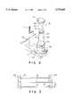
- FIG. 2is a perspective view of one example of a ladder boat used in the heat treatment process according to the first embodiment of the present invention.
- FIG. 3is a vertical sectional view of grooves of the ladder boat of FIG. 2, and the state of wafers supported in the grooves.
- FIG. 4is a characteristic curve of a pattern of temperature raising rates in the vertical heat treatment furnace according to the first embodiment of the present invention.
- FIG. 5is a graph of relationships between wafer temperature and silicon yield shearing stresses.
- FIG. 6is a diagrammatic view of the heat treatment apparatus according to a second embodiment of the present invention.
- FIG. 7is a vertical sectional view of the heat treatment apparatus as illustrated in FIG. 6.
- FIG. 8is an enlarged vertical sectional view of the wafer support portion of the ladder boat of the heat treatment apparatus as shown in FIG. 6.
- FIG. 9is a plan view showing parts of a wafer where slips occur according to the conventional heat treatment process.
- FIG. 1is a vertical sectional view of the vertical heat treatment apparatus for practicing the process according to a first embodiment of the present invention, which explains the general structure of the apparatus.
- a vertical heat treatment furnace 20comprises a heating unit 3 enclosing a reaction tube 2.
- the reaction tube 2comprises a tube of a heat resistant, corrosion resistant material (e.g., quartz) having, for example, the upper end closed and the lower end opened.
- a liner tube 21 of, e.g., quartzencloses the reaction tube 21.
- the heating unit 3comprises a plurality of stages of heating blocks provided on the inside surface of a heat insulator 31 in such a manner as to enclose the liner tube 21.
- Each heating blockis made of a resistance heating wire 32 vertically wound along the inside circumferential surface of the heat insulator 31.
- a material of the resistance heating wire 32can be, e.g., molybdenum disilicate (MoSi 2 ) to enable hig-speed temperature rise and fall.
- the heating wires 32can raise an internal temperature of the reaction tube 2 at a high temperature increasing rate of 50°-100° C.
- a thermocouple TCis provided on each heating wire 32 for measuring temperatures of the heating wire 32.
- a processing gas feed pipe 41which is connected to gas supply sources not shown is inserted in the reaction tube 2.
- the forward end 41a of the gas feed pipe 41is extended up to a position where the forward end 41a is opposed to the ceiling of the reaction tube 2.
- An exhaust pipe 43 connected to a vacuum pump 42is provided in the reaction tube 2.
- a boat elevator 51which is moved up and down on a screw rod 51a (see FIG. 2).
- a cap 52is mounted on the boat elevator 51.
- the cap 52air-tightly closes the open bottom of the reaction tube 2 when the cap 52 is at its uppermost position.
- a ladder boat 6which is a holder is provided on the cap 52 with a heat insulating cylinder 53 provided therebetween.
- four support rods of, e.g., quartzare provided between an upper plate 61 and a bottom plate 62 vertically opposed to each other with a required interval therebetween.
- the four support rods 63-66are so arranged that two 63, 64 of the four support rods 63-66 support the upper and the bottom plates 61, 62 at the left and the right of the forward side in the direction of advance of a wafer transfer fork 60 into the ladder boat 6, and the rest two support rods 65, 66 support the upper and the bottom plates at the left and the right of the backward side in the direction of advance of the wafer transfer fork 60 into the ladder boat 6.
- grooves 67having a little larger vertical length than a thickness of wafers W so that the wafers W can be inserted in the grooves with the undersides of the peripheral edges supported therein are formed in the respective support rods 63-66.
- the wafers Ware placed into the grooves 67 and taken out of the grooves 67 by the transfer fork 60 through the two forward support rods 63, 64.
- the grooves 67are provided at a pitch (d) of 3/16 inches.
- An arrangement pitch (p) of the wafers W inserted in the grooves 67(a distance between the underside of each wafer W and that of a next below one W) is 3/16 inches.
- Air inlets 71, and air outlets 72are provided respectively in the upper end and in the bottom of the vertical heat treatment furnace 20 between the heating unit 3 and the reaction tube 2.
- the air inlets 71 and the air outlets 72are provided in the reaction tube 2 circumferentially at four positions. Blower fans and exhaust fans not shown are provided respectively in the air inlets 71 and in the air outlets 72. Forced cooling means is thus constituted for forcedly cooling the interior of the reaction tube 2.
- the interior of the reaction tube 20is set at 400° C.
- Sixty sheets, for example, of wafers W held on the ladder boat 6are loaded into the reaction tube 2 by the boat elevator 51 through the opened bottom thereof.
- a vertical pitch of the grooves 67 (FIG. 3) formed in the ladder boat 6is, e.g., 3/16 inches.
- the wafers W held in the grooves 67 of this pitchhave an arrangement pitch of 3/16 inches.
- the heat treatment region in the reaction tube 2being about 900° C. means that because the region where those of objects-to-be-treated, wafers W held on the ladder boat except the top and the bottom dummy wafers are arranged does not have a perfectly uniform temperature distribution, the heat treatment region has a temperature range of, e.g., 900° C. plus or minus a temperature difference of the temperature distribution.
- the 34° C. temperature increasing rateis not a set value for the control unit but a temperature increasing rate actually measured in the heat treatment region in the reaction tube 2 by TCs.
- the temperature increasing rateis decreased in steps or continuously between 900° C. and 980° C.
- the temperature in the reaction tube 2is raised at, e.g., above 9° C./minute, a low temperature increasing rate of, e.g., about 10° C./minute, and between 980° C. and 1100° C. the temperature in the reaction tube 2 is raised at about a 5° C./minute temperature increasing rate.
- required oxidation gasese.g., O 2 gas and HCl gas are fed into the reaction tube 2 through the gas feed pipe 41 while the interior of the reaction tube 2 is exhausted through the air outlets 43 to maintain a required pressure, e.g., the normal pressure in the reaction tube 2. In this state the wafers are oxidized.
- a preparatory step for a next processis conducted.
- the interior of the reaction tube 2is purged with an inert gas (e.g., N 2 gas) while as shown in FIG. 4, the temperature of the interior of the reaction tube is lowered down to 980° C. at a set temperature decreasing rate (e.g., 8° C./minute) and subsequently down to 900° C. at an about 15° C./minute temperature decreasing rate.
- airis forcedly blown between the reaction tube 2 and the heating unit 3 through the air inlets 71 while exhausted through the air outlets 72, whereby the interior of the reaction tube 2 is forcedly cooled down to, e.g., 400° C. at an about 30° C./minute temperature decreasing rate, and then the cap 52 is opened to unload the ladder boat out of the reaction tube 2.
- Temperature increasing ratesare averages of temperatures of a wafer in the tenth grooves (indicated by “10” on the left in TABLE 1) of the ladder boat from the bottom and of a wafer in the thirteenth grooves (indicated by "31” on the left in TABLE 1) from the bottom by thermocouples at totally 4 positions, i.e., the quarters of the circumference which is 10 mm inner of the circumferential edge, and the center.
- a temperature increasing ratewas as high as 14° C./minute from 900° to 980° C., no slip took place. Thus it is found that no slip occurs with a temperature increasing rate of below 14° C./minute or below 6° C./minute from 900° to 980° C. and from 980° to 1100° C. Accordingly, a temperature increasing rate is lowered in steps (two steps in the above-described embodiment) in the ranges of temperatures above 900° C. A threshold temperature increasing rate pattern which causes no slip is determined in advance, and based on the determined temperature raising rate pattern, temperature increasing rates are set, whereby slips in the wafers can be precluded, and high throughputs can be obtained.
- the temperature decreasing processis considered to be the same as the temperature increasing process. It is difficult to control the temperature decreasing process. It is preferred that blowing rates of the forced cooling means are adjusted to give a threshold temperature decreasing rate pattern.
- a reason for thisis considered to be that a larger spacing between each of the wafers and its adjacent one permits radiation from the surrounding heating unit 3 to directly reach the central part of the wafers with a result that intra-surface temperature uniformity of the wafers transiently becomes higher.
- occurrence of slipscan be prevented by raising the temperatures at lower temperature increasing rates lower than the above-described respective threshold temperature increasing rate.
- threshold temperature increasing ratesthus change depending on wafer arrangement pitches
- threshold temperature increasing ratesare found by changing a temperature increasing rate pattern for a wafer arrangement pitch, and a temperature increasing pattern is set, based on the threshold temperature increasing rate pattern.
- a temperature increasing rate patternis set for operation of the heat treatment apparatus.
- the ladder boat as shown in FIG. 2which is easy for wafers to be transferred to and from, and which is inexpensive, is used, and occurrence of slips can be prevented while a treatment is conducted at high throughputs.
- An industrial advantageous heat treatment processcan be provided.
- the threshold temperature increasing rateis low especially above 900° C. and becomes lower for higher heating temperature ranges.
- the temperatureis raised at a high temperature increasing rate up to 900° C., and thereafter the rate is lowered in steps.
- the heat treatment apparatusis expected to be more improved and allow higher temperature increasing rates.
- the heat treatment process according to the present inventionis effective to use such improved heat treatment apparatus.
- the present inventionis applied to the ladder boat but is applicable to the ring boat.
- slipscan be prevented in loading a number of wafers into a heat treatment furnace and heat-treating the same.
- FIG. 5is a graph of relationships between wafer temperatures and silicon yield shearing stresses based on "Macroscopic plastic properties of dislocation-free germanium and other semiconductor crystals. 1. Yield behavior" which is a study of silicon yield stress referred to in IEEE “TRANSACTION ON SEMICONDUCTOR MANUFACTURING", Vol. 1, No. 3 (March 1988).
- the yield shearing stress(kgf/mm 2 ) abruptly lowers at around 500° C., somewhat slowly lowers at 600°-800° C. and thereafter smoothly lowers. Based on this silicon characteristic, it is found that because the yield stress value decreases are larger at higher treatment temperatures, allowable intra-surface temperature differences which cause no slips in wafers are accordingly smaller.
- the intra-surface temperature differencescan be smaller at larger pitches of wafers arranged one above another. As described above, the intra-surface temperature difference is larger at higher temperature increasing rates. In connection with productivity, the batch processing has no merit unless wafers can be processed more efficiently than the sheet processing.
- wafer mounting pitcheswhich can restrict intra-surface temperature differences to allowed temperature differences which cause no slip are given in accordance with treatment temperatures.
- the mounting pitch in the present inventionis a distance between the middle of a thickness of a wafer and that of a thickness of a lower next wafer, i.e., a distance between the upper end surface of one of wafers mounted parallel with each other one above another on a ladder boat.
- FIG. 6is a diagrammatic view of a heat treatment apparatus 101 according to the second embodiment of the present invention.
- FIG. 7is a vertical sectional view of the heat treatment apparatus 101.
- a set number, for example 25 sheets, of silicon semiconductor wafers (hereinafter called "wafer"), objects to be treated, having a large diameter of above 250 mm, e.g., 300 mmare mounted, spaced one above another, on a ladder boat 110 as mounting jig disposed below the heat treatment apparatus 101 and are loaded into a reaction vessel 103 in a vertical furnace of the heat treatment apparatus on the lifted ladder boat 110 to be subjected to a required heat treatment, e.g., formation of, e.g., a silicon oxide film.
- the ladder boat 10comprises a disc-shaped top plate 111 and a disc-shaped bottom plate 112, and three support rods 113, 114, 115 provided between the top plate 111 and the bottom plate 112, whereby a mounting portion is defined.
- Wafers carried in by carrying means 124, e.g., a carrier arm or othersare placed in grooves 116 formed in the insides of the support rods 113, 114, 115 to be mounted on the ladder boat 110 in a horizontal direction
- a plurality of the groovesare formed in each support rod 113, 114, 115 in the direction of length. As shown in FIG. 8, a pitch of the grooves is so set that a pitch of the mounted wafers W is within a range of 10-160 mm, e.g., 40 mm.
- the ladder boat 110 having such structureis removably mounted at a support member 122 thereof on a quartz heat insulation cylinder 121 with a flange 120 of, e.g., stainless steel.
- the heat insulation cylinder 121is mounted on a boat elevator 123 which is movable up and down.
- the boat elevator 123is lifted to load the wafers W on the ladder boat 110 at a set position in a reaction tube 103 in a vertical furnace 102.
- a casing 104 of the vertical furnace 102has the lower end secured to the top surface of a base plate 105.
- the casing 104has a substantially cylindrical shape the top surface of which is flat and has the inside surface covered with a heat insulating material 106.
- a heater 107On the inside circumferential surface of the casing 104 there is provided a heater 107 in, e.g., a helix (coil) which is formed of a resistance heater, as of molybdenum disilicide.
- a liner tube 108 of, e.g., SiCis provided between the heater 107 and the reaction vessel 103, surrounding the reaction vessel 103.
- the heater 107by suitable temperature control means (not shown), heats the interior of the reaction vessel 103 uniformly up to an arbitrary temperature, e.g., 600°-1000° C. in a 300°-1100° C. temperature range and maintains the arbitrary temperature.
- the reaction vessel 103which has a processing region therein, has, as described above, a substantially tubular shape having the flat top surface and is vertically erected by means of the flange on the lower end thereof on a base plate (not shown) which is other than the base plate 105.
- a gas discharge plate 133is provided upper inside the reaction vessel 103 in parallelism with a ceiling 132 of the reaction vessel 103.
- a number of gas discharge holes 134are formed in the gas discharge plate 133.
- a space S defined by the gas discharge plate 133, the top plate 132, etc.forms the so-called processing gas preparatory chamber.
- a processing gas supplied into the space Sis discharged uniformly through the gas discharge holes 134 onto the wafers loaded in the reaction vessel 103.
- a processing gas for forming silicon oxide filme.g., O 2 (oxygen gas) is led through a processing gas feed pipe 141 provided along an outside of the reaction vessel 103 to be introduced into the space S defined upper inside the reaction vessel 103 through processing gas discharge holes 141A, and then discharged into the reaction vessel 103 through the processing gas discharge holes 134.
- the processing gas which has reacted for processingis discharged outside through a discharge pipe 142 provided in a lower part of the reaction vessel 103.
- the heater 107is heated to raise an internal temperature of the reaction vessel 103 up to, e.g., about 600° C. while N 2 gas is introduced into the reaction vessel 103 through the processing gas feed pipe 141 to place the interior of the reaction vessel 103 in an N 2 gas atmosphere. Then, wafers W, objects to be treated, are mounted on the ladder boat 110, then the boat elevator 132 is lifted to raise the ladder boat to a position where, as shown in FIG.
- the flange 120 of the heat insulation cylinder 121is brought into close contact with the flange 131 of the lower part of the reaction vessel 103 to thereby load the wafers W in the reaction vessel 103, and air-tightly close the reaction vessel 103.
- the interior of the reaction vessel 103is heated to a required processing temperature, e.g., 1000° C., and O 2 (oxygen) gas is supplied into the reaction vessel 103 through the processing gas feed pipe 141 while the interior of the reaction vessel 103 is exhausted through the discharge pipe 142 to maintain the interior of the reaction vessel 103 under the atmospheric pressure.
- a required processing temperaturee.g. 1000° C.
- O 2 (oxygen) gasis supplied into the reaction vessel 103 through the processing gas feed pipe 141 while the interior of the reaction vessel 103 is exhausted through the discharge pipe 142 to maintain the interior of the reaction vessel 103 under the atmospheric pressure.
- the heat treatmentis conducted for a required period of time.
- a silicon oxide film (SiO 2 ) film of a required thicknessis formed on the surfaces of the wafers W.
- the above-described temperature increase from the pre-heating temperature 600° C. to the processing temperature 1000° C.must be conducted at high rates so as to improve throughputs, take advantage of the batch processing, and lower thermal budget in terms of processing.
- the wafers Wwhich are objects to be treated by the heat treatment apparatus according to the second embodiment, are 300 mm-diameter wafers, which are considerably larger than the conventional 200 mm-diameter wafers.
- the wafers W mounted at the conventional mounting pitchwill have large differences in heat radiation amount from the heater 107 between the peripheral parts thereof and the central parts thereof. As a result, the wafers W have large intra-surface temperature differences, which cause slips in the wafers W.
- the ladder boat 110 used in the second embodimenthas a 40 mm pitch as described above, which decreases intra-surface temperature differences in the wafers to thereby preclude occurrences of slips.
- the inventors of the present inventionhad simulations to prove the advantage.
- the internal temperature increase of the reaction vessel 103 from 600° C. to 1000° C.was raised at a high rate of 100° C./min, and the intra-surface temperature difference of the wafers W could be suppressed to 10° C. This intra-surface temperature difference will generate no slip.
- wafersare mounted at a 10 mm mounting pitch, and the internal temperature of the reaction vessel 103 was raised at the same rate.
- the intra-surface temperature difference of the waferswas even 130° C. when the temperature passed 900° C.
- the heat treatment apparatus according to the second embodimentcan suppress intra-surface temperature differences smaller than the conventional heat treatment apparatus which uses the high-rate temperature increasing process in a heat treatment.
- the oxidationtakes a longer period of time, throughput differences are larger, and the second embodiment has much higher productivity than the sheet heat treatment apparatus. Accordingly large-diameter wafers of a 300 mm diameter can be heat treated with higher productivity than the sheet heat treatment apparatus and even without occurrence of slips.
- the second embodimentis applied to an atmospheric pressure-heat treatment apparatus for oxidation and diffusion, but is also applicable to low-pressure heat treatment apparatuses, e.g., low-pressure CVD apparatuses.
- the heat treatment apparatusin a case that large-diameter wafers of an above 250 mm diameter are heat treated, can use the batch processing, using a mounting jig for mounting a plurality of wafers without occurrence of slips. No slip occurs in the wafers even with a process of a temperature increase of 20° C./min. Good throughputs can be accordingly obtained, and higher productivity can be attained than sheet heat treatment apparatuses.
Landscapes
- Chemical & Material Sciences (AREA)
- Engineering & Computer Science (AREA)
- Materials Engineering (AREA)
- Metallurgy (AREA)
- Organic Chemistry (AREA)
- Crystallography & Structural Chemistry (AREA)
- General Chemical & Material Sciences (AREA)
- Chemical Kinetics & Catalysis (AREA)
- Mechanical Engineering (AREA)
Abstract
Description
This application is a continuation-in-part of application Ser. No. 08/441,048; filed on May 15, 1995 now U.S. Pat. No. 5,688,116.
The present invention is directed to apparatus for conducting batch heat treatments on a plurality of objects.
Processing of, e.g., semiconductor wafers (hereinafter called "wafers") includes heat treatments at high temperatures. This processing forms oxide films on the wafers, diffusing dopants, and others. Horizontal heat treatment furnaces have conventionally been dominant for conducting heat treatments. But recently, vertical heat treatment furnaces are increasingly used because of their homogeneous wafer intra-surface treatment, easy loading and unloading of the wafers, little entrainment of outside air into the furnaces, etc.
A vertical heat treatment apparatus using such a vertical heat treatment furnace includes a ladder boat; A ladder boat is one kind of a vertical wafer boat which holds a number of wafers vertically spaced from each other. The wafers the can be loaded and unloaded and out of the heat treatment furnace. The ladder boat comprises a top plate and a bottom plate vertically opposing each other, four support rods of, e.g., quartz provided between the top and the bottom plates. Grooves are formed in the respective support rods into which the peripheral edges of wafers are inserted in a set direction (for example, in a horizontal direction).
When a set number (e.g., 50 sheets) of wafers W have been mounted on the ladder boat, an elevator is used to load the ladder boat into the heat treatment furnace, then a required batch heat treatment on the wafers can be performed. Especially recently, higher speed heat treatments and higher throughputs are required in accordance with higher integration (e.g., above 60 M) and larger sizes (12 inches) of wafers.
Because silicon which is a base material of the wafers has a melting point of 1410° C., crystal defects called slip (the parts indicated by S in FIG. 9) tend to take place in vicinities of parts of the wafers supported by thesupport rods
Causes for the occurrence of the slips are: 1) internal stresses due to tare weights of the wafers; and 2) thermal strain stresses due to intra-surface temperature disuniformity of the wafers. That is, although a mechanism for the occurrence is not clear, it is considered in connection with cause 1) that because the wafers are supported by the ladder boat at the peripheral edges, supported partially at four positions, large internal stresses take place due to tare weights of the wafers being heat-treated in vicinities of the supported parts. When the internal stresses exceed a certain magnitude, the slips occur. Furthermore, even wafers having specification values have "sori", and get additional sori due to temperature distributions when heated. In addition, the grooves in the support rods have machining errors. If one of the supported parts of a wafer should come out of the associated groove, the wafer is supported at three parts, and loads born by the respective supported parts are unbalanced. Consequently it often takes place that large stresses exceeding a threshold for the occurrence of the slips are generated at, e.g., one of the supported parts.
In connection with the cause 2), heat is conducted to and from the wafers via the support rods of the heat treatment boat when the wafers are heated, and temperature differences take place between the central parts of the wafers and the peripheral edges thereof and cause thermal strain stresses. It is considered that the slips occur when the thermal strain stresses exceed a certain magnitude. On the other hand, recently the structure of the heat treatment furnace itself, and the heater have been improved, and heat treatment furnaces whose low internal temperatures can be raised at a rate as high as, e.g., 100° C./minute are fabricated. Such a high-speed furnace can decrease thermal budget and can improve throughputs. On the other hand, the furnace has a disadvantage that intra-furnace temperature differences are increased upon temperature increase and decrease, and larger thermal strain stresses take place in the wafers, and the slips take place especially when the wafers are heat-treated at high temperatures approximate to the melting point of the base material of the wafers. To solve this problem, various discussion have been made on the structure of the wafer boat. For example, a wafer boat typically a called "ring boat" is often used. In the ring boat, wafers are not supported by grooves formed in the support rods of the boat. Rings instead are supported in the grooves, and wafers are held directly on the rings. The peripheral edges of the wafers surface-contact with the rings, and internal stresses of the wafers are mitigated, whereby the occurrence of the slips can be. The ring boat, however, is difficult to fabricate and.
But the ring boat is difficult to fabricate and expensive. Furthermore, a robot carrier arm cannot enter between the support rods when wafers are transferred, as can in the ladder boat. Thus a mechanism for pushing up the wafers from below to load the wafers is necessary, which makes the structure of the wafer carrier system complicated. This is also a problem. In addition, it is much required to preclude the slips without changing the structure of the wafer boat.
The present invention was made in view of these problems. An object of the present invention is to provide a heat treatment process which can preclude occurrence of slips in a heat treatment.
The present invention relates to a heat treatment apparatus for holding a number of objects to be treated by a holding means at a vertical interval and loading the holding means into a heat treatment furnace. The objects-to-be-treated then being heat-treated while temperatures in the heat treatment furnace are controlled. The controlled temperature increasing pattern has a smaller temperature increasing rate gradient than a threshold temperature increasing rate pattern for preset heat treating temperatures, which is able to prevent occurrence of slips in the objects-to-be-treated.
It is considered that slips taking place when wafers are heat-treated occur when thermal strain stresses become large when the wafers are heated to some extent. According to the applicant's experiments, slips were observed in a range of temperatures above a heating temperature of 900° C. unless wafers were considerably gradually heated. Here the range of high temperatures includes different threshold temperature increasing rate patterns for a range of, e.g., 900°-980° C. and a range of temperatures above the former. Such threshold temperature increasing rate patterns depend on vertical arrangement pitches of the wafers.
In accordance with the present invention, a heat treatment is conducted with the arrangement pitch set at a required value and a substantial threshold temperature increasing rate pattern given for the high temperature ranges. Temperatures can be effectively raised and lowered, high throughputs can be obtained, and in addition occurrence of slips can be prevented. Threshold temperature increasing and decreasing rates for prevention of slips become lower as temperatures rise. In a high temperature range of above 900° C., for example, the temperature is raised in two steps of, e.g., 13° C. and 5° C., whereby a heat treatment can be conducted effectively without occurrence of slips.
FIG. 1 is a vertical sectional view of one example of the vertical heat treatment apparatus used for the heat treatment process according to a first embodiment of the present invention.
FIG. 2 is a perspective view of one example of a ladder boat used in the heat treatment process according to the first embodiment of the present invention.
FIG. 3 is a vertical sectional view of grooves of the ladder boat of FIG. 2, and the state of wafers supported in the grooves.
FIG. 4 is a characteristic curve of a pattern of temperature raising rates in the vertical heat treatment furnace according to the first embodiment of the present invention.
FIG. 5 is a graph of relationships between wafer temperature and silicon yield shearing stresses.
FIG. 6 is a diagrammatic view of the heat treatment apparatus according to a second embodiment of the present invention.
FIG. 7 is a vertical sectional view of the heat treatment apparatus as illustrated in FIG. 6.
FIG. 8 is an enlarged vertical sectional view of the wafer support portion of the ladder boat of the heat treatment apparatus as shown in FIG. 6.
FIG. 9 is a plan view showing parts of a wafer where slips occur according to the conventional heat treatment process.
FIG. 1 is a vertical sectional view of the vertical heat treatment apparatus for practicing the process according to a first embodiment of the present invention, which explains the general structure of the apparatus. A verticalheat treatment furnace 20 comprises aheating unit 3 enclosing a reaction tube 2. The reaction tube 2 comprises a tube of a heat resistant, corrosion resistant material (e.g., quartz) having, for example, the upper end closed and the lower end opened. Aliner tube 21 of, e.g., quartz encloses thereaction tube 21. Theheating unit 3 comprises a plurality of stages of heating blocks provided on the inside surface of aheat insulator 31 in such a manner as to enclose theliner tube 21. Each heating block is made of aresistance heating wire 32 vertically wound along the inside circumferential surface of theheat insulator 31. A material of theresistance heating wire 32 can be, e.g., molybdenum disilicate (MoSi2) to enable hig-speed temperature rise and fall. Theheating wires 32 can raise an internal temperature of the reaction tube 2 at a high temperature increasing rate of 50°-100° C. A thermocouple TC is provided on eachheating wire 32 for measuring temperatures of theheating wire 32.
A processinggas feed pipe 41 which is connected to gas supply sources not shown is inserted in the reaction tube 2. Theforward end 41a of thegas feed pipe 41 is extended up to a position where theforward end 41a is opposed to the ceiling of the reaction tube 2. Anexhaust pipe 43 connected to avacuum pump 42 is provided in the reaction tube 2.
Below the reaction tube 2 there is provided aboat elevator 51 which is moved up and down on a screw rod 51a (see FIG. 2). Acap 52 is mounted on theboat elevator 51. Thecap 52 air-tightly closes the open bottom of the reaction tube 2 when thecap 52 is at its uppermost position. Aladder boat 6 which is a holder is provided on thecap 52 with aheat insulating cylinder 53 provided therebetween. As shown in FIG. 2, four support rods of, e.g., quartz are provided between anupper plate 61 and abottom plate 62 vertically opposed to each other with a required interval therebetween. The four support rods 63-66 are so arranged that two 63, 64 of the four support rods 63-66 support the upper and thebottom plates wafer transfer fork 60 into theladder boat 6, and the rest twosupport rods wafer transfer fork 60 into theladder boat 6.
As enlarged in FIG. 3,grooves 67 having a little larger vertical length than a thickness of wafers W so that the wafers W can be inserted in the grooves with the undersides of the peripheral edges supported therein are formed in the respective support rods 63-66. The wafers W are placed into thegrooves 67 and taken out of thegrooves 67 by thetransfer fork 60 through the twoforward support rods grooves 67 are provided at a pitch (d) of 3/16 inches. An arrangement pitch (p) of the wafers W inserted in the grooves 67 (a distance between the underside of each wafer W and that of a next below one W) is 3/16 inches.
Next, the first embodiment of the heat treatment process conducted by the above-described vertical heat treatment apparatus will be explained. First, the interior of thereaction tube 20 is set at 400° C. Sixty sheets, for example, of wafers W held on theladder boat 6 are loaded into the reaction tube 2 by theboat elevator 51 through the opened bottom thereof. A vertical pitch of the grooves 67 (FIG. 3) formed in theladder boat 6 is, e.g., 3/16 inches. The wafers W held in thegrooves 67 of this pitch have an arrangement pitch of 3/16 inches.
Then, electric power is supplied to theresistance heating wires 32 from the outside. The power supply is so controlled that, as shown in FIG. 4, the interior of the reaction tube 2 is heated at a high temperature increasing rate of above 100° C., e.g., 34° C./minute until the heat treatment region in the reaction tube 2 has a temperature of about 900° C. Here, the heat treatment region in the reaction tube 2 being about 900° C. means that because the region where those of objects-to-be-treated, wafers W held on the ladder boat except the top and the bottom dummy wafers are arranged does not have a perfectly uniform temperature distribution, the heat treatment region has a temperature range of, e.g., 900° C. plus or minus a temperature difference of the temperature distribution. Hereinafter this is the same with a temperature of the interior of the reaction tube 2. The 34° C. temperature increasing rate is not a set value for the control unit but a temperature increasing rate actually measured in the heat treatment region in the reaction tube 2 by TCs.
When a temperature of the heat treatment region in the reaction tube 2 has reached 900° C., as shown in FIG. 4, the temperature increasing rate is decreased in steps or continuously between 900° C. and 980° C. For example, the temperature in the reaction tube 2 is raised at, e.g., above 9° C./minute, a low temperature increasing rate of, e.g., about 10° C./minute, and between 980° C. and 1100° C. the temperature in the reaction tube 2 is raised at about a 5° C./minute temperature increasing rate. When the temperature in the reaction tube has reached, e.g., about 1,100° C., required oxidation gases, e.g., O2 gas and HCl gas are fed into the reaction tube 2 through thegas feed pipe 41 while the interior of the reaction tube 2 is exhausted through theair outlets 43 to maintain a required pressure, e.g., the normal pressure in the reaction tube 2. In this state the wafers are oxidized.
Following a preset time of the oxidation, a preparatory step for a next process is conducted. For example, the interior of the reaction tube 2 is purged with an inert gas (e.g., N2 gas) while as shown in FIG. 4, the temperature of the interior of the reaction tube is lowered down to 980° C. at a set temperature decreasing rate (e.g., 8° C./minute) and subsequently down to 900° C. at an about 15° C./minute temperature decreasing rate. Then, air is forcedly blown between the reaction tube 2 and theheating unit 3 through theair inlets 71 while exhausted through theair outlets 72, whereby the interior of the reaction tube 2 is forcedly cooled down to, e.g., 400° C. at an about 30° C./minute temperature decreasing rate, and then thecap 52 is opened to unload the ladder boat out of the reaction tube 2.
As evident from the following experimental results, by the heat treatment process according to the present invention, no slips occur in the wafers W, and high throughputs can be obtained. That is, presence of slips was checked in 6-inch wafers W held on the ladder boat at a vertical wafer arrangement pitch of 3/16 inches and at various temperature increasing rates. In the temperature increasing rate pattern, the temperature (400° C. ) at which the wafers W were loaded was raised to 900° C. at a high rate (e.g., 30° C./minute) and raised at the low rate in the temperature range of above 900° C. TABLE 1 shows the temperature ranges, temperature increasing rates and presence of slips. Temperature increasing rates are averages of temperatures of a wafer in the tenth grooves (indicated by "10" on the left in TABLE 1) of the ladder boat from the bottom and of a wafer in the thirteenth grooves (indicated by "31" on the left in TABLE 1) from the bottom by thermocouples at totally 4 positions, i.e., the quarters of the circumference which is 10 mm inner of the circumferential edge, and the center.
TABLE 1 ______________________________________ (Wafer arrangement pitch: 3/16 inches) Groove Temperature Range °C. Pres-Ordinal 400˜ 900˜ 980˜ 1100˜ 980˜ 900˜ence Number 900 980 1100 980 900 400 of Slip ______________________________________ °C./Min TEST 10 34 11 11 7 14 30 present RUN 1 31 31 13 13 7 24 29TEST 10 34 11 7 7 14 30 present RUN 2 31 31 13 7 7 14 29TEST 10 34 11 6 7 14 30absent RUN 3 31 31 13 6 7 14 29TEST 10 43 12 5 7 14 30 absent RUN 4 31 43 14 5 7 14 29TEST 10 43 17 5 7 14 30 present RUN 5 31 43 19 5 7 14 29TEST 10 43 12 5 10 16 30present RUN 6 31 43 14 5 16 16 29 ______________________________________
By checking presence of slips in various temperature increasing rate patterns (for example, visually confirming presence of slips and reconfirm by a 100-magnification metal microscope or etching), suitable temperature increasing rates can be found. That is, as shown in TABLE 1, in Test Run 1, in which a temperature increasing rate was 13° C./minute from 900° to 1100° C. (the higher one of the temperature increasing rates of the tenth and the thirteenth wafers from the bottom of theladder boat 6 was taken), slips occurred. But no slip took place as inTest Run 3, in which a temperature increasing rate was as low as 6° C./minute in the range of temperatures above 980° C.In Test Runs 3 and 4, a temperature increasing rate was as high as 14° C./minute from 900° to 980° C., no slip took place. Thus it is found that no slip occurs with a temperature increasing rate of below 14° C./minute or below 6° C./minute from 900° to 980° C. and from 980° to 1100° C. Accordingly, a temperature increasing rate is lowered in steps (two steps in the above-described embodiment) in the ranges of temperatures above 900° C. A threshold temperature increasing rate pattern which causes no slip is determined in advance, and based on the determined temperature raising rate pattern, temperature increasing rates are set, whereby slips in the wafers can be precluded, and high throughputs can be obtained.
As in Test Run 4, no slip took place even at a high temperature increasing rate of, e.g., 43° C./minute in the range of temperatures below 900° C. This agrees with the inventors'finding in their preparatory experiments that temperature increasing rates become very influential at temperatures above about 900° C. Therefore, it is necessary that the interior of the reaction tube 2 is heated at a high temperature increasing rate up to 900° C. after the ladder boat has been loaded into the reaction tube 2, and the temperature is raised in steps at low temperature increasing rates in the ranges of temperatures above 900° C. so as to ensure high throughputs without slips.
The temperature decreasing process is considered to be the same as the temperature increasing process. It is difficult to control the temperature decreasing process. It is preferred that blowing rates of the forced cooling means are adjusted to give a threshold temperature decreasing rate pattern.
The reason the temperature increasing rate has to be lowered in the ranges of temperatures above 900° C., as described above, is that the base material, silicon, whose melting point is 1,410° C., becomes sensitive to internal stresses when a heating temperature is above about 900° C., The sensitivity increases with increases of the heating temperature. It is considered that unless the temperature increasing rate is low, slips occur.
Six-inch wafers, as wafers W, as used in the above-described experiment, were arranged on the ladder boat at a 3/8 inch arrangement pitch. The presence of slips was then checked for the respective temperature increasing rates of various temperature increasing rate patterns by the use of the same apparatus (FIG. 1) as in the above-described experiment. The result is shown in TABLE 2.
TABLE 2 ______________________________________ (Wafer arrangement pitch: 3/8 inches) Groove Temperature Range °C. Pres-Ordinal 400˜ 900˜ 980˜ 1100˜ 980˜ 900˜ence Number 900 980 1100 980 900 400 of Slip ______________________________________ °C./Min TEST 10 62 17 12 13 14 34 present RUN 1 31 54 18 12 13 14 34TEST 10 62 17 9 13 14 34 present RUN 2 31 54 18 9 13 14 34TEST 10 62 17 8 13 14 34absent RUN 3 31 54 18 8 13 14 34TEST 10 62 18 7 13 14 34 absent RUN 4 31 54 19 7 13 14 34TEST 10 62 23 7 13 14 34 present RUN 5 31 54 23 7 13 14 34TEST 10 62 23 7 7 22 34present RUN 6 31 54 23 7 7 22 34 ______________________________________
As evident from the results of RUN 2 andRUN 3 in TABLE 2, no slip occurs in the wafers in the temperature range of 980°-1,100° C. at a temperature increasing rate of below 8° C./minute. As evident from the result ofRUN 3 and RUN 4 in TABLE 2, no slip takes place in the temperature range of 900°-980° C. at a temperature increasing rate of 18° C./minute. Here the case of 3/16 inch arrangement pitch of wafers on the ladder boat, and that of 3/8 inch arrangement pitch will be compared with each other. Setting the wafers at the 3/8 inch arrangement pitch resulted in the higher threshold temperature increasing rate for the absence of slips. Accordingly it is found that wider wafer arrangement pitch is effective for ensuring prevention of occurrence of slips. A reason for this is considered to be that a larger spacing between each of the wafers and its adjacent one permits radiation from the surroundingheating unit 3 to directly reach the central part of the wafers with a result that intra-surface temperature uniformity of the wafers transiently becomes higher. Based on the above-described experimental results, in cases of wafer arrangement pitches above the 3/16 inch arrangement pitch, and cases of wafer arrangement pitches above the 3/8 inches, occurrence of slips can be prevented by raising the temperatures at lower temperature increasing rates lower than the above-described respective threshold temperature increasing rate.
Because threshold temperature increasing rates thus change depending on wafer arrangement pitches, threshold temperature increasing rates are found by changing a temperature increasing rate pattern for a wafer arrangement pitch, and a temperature increasing pattern is set, based on the threshold temperature increasing rate pattern. Thus a temperature increasing rate pattern is set for operation of the heat treatment apparatus. As a result, without using the ring boat, which is difficult for wafers to be transferred to and from, and which is expensive, the ladder boat as shown in FIG. 2, which is easy for wafers to be transferred to and from, and which is inexpensive, is used, and occurrence of slips can be prevented while a treatment is conducted at high throughputs. An industrial advantageous heat treatment process can be provided. The threshold temperature increasing rate is low especially above 900° C. and becomes lower for higher heating temperature ranges. Accordingly it is preferred to prevent occurrence of slips and obtain high throughputs that the temperature is raised at a high temperature increasing rate up to 900° C., and thereafter the rate is lowered in steps. In future the heat treatment apparatus is expected to be more improved and allow higher temperature increasing rates. The heat treatment process according to the present invention is effective to use such improved heat treatment apparatus. The present invention is applied to the ladder boat but is applicable to the ring boat.
As described above, according to the present invention, slips can be prevented in loading a number of wafers into a heat treatment furnace and heat-treating the same.
Next, the heat treatment apparatus according to a second embodiment of the present invention will be explained.
According to a finding of the inventors of the present invention, occurrence of slips in wafers much depend on yield values of the shearing stress of silicon which is a material of the wafers. It is also generally known that the yield shearing stress much depends on silicon temperatures.
FIG. 5 is a graph of relationships between wafer temperatures and silicon yield shearing stresses based on "Macroscopic plastic properties of dislocation-free germanium and other semiconductor crystals. 1. Yield behavior" which is a study of silicon yield stress referred to in IEEE "TRANSACTION ON SEMICONDUCTOR MANUFACTURING", Vol. 1, No. 3 (August 1988).
In FIG. 5, the yield shearing stress (kgf/mm2) abruptly lowers at around 500° C., somewhat slowly lowers at 600°-800° C. and thereafter smoothly lowers. Based on this silicon characteristic, it is found that because the yield stress value decreases are larger at higher treatment temperatures, allowable intra-surface temperature differences which cause no slips in wafers are accordingly smaller.
In the system in which wafers are heated by radiation heat from a tubular furnace, it is considered that the intra-surface temperature differences can be smaller at larger pitches of wafers arranged one above another. As described above, the intra-surface temperature difference is larger at higher temperature increasing rates. In connection with productivity, the batch processing has no merit unless wafers can be processed more efficiently than the sheet processing.
According to the heat treatment apparatus of the second embodiment of the present invention wherein the inventors have made in the above-described background, wafer mounting pitches which can restrict intra-surface temperature differences to allowed temperature differences which cause no slip are given in accordance with treatment temperatures. The mounting pitch in the present invention is a distance between the middle of a thickness of a wafer and that of a thickness of a lower next wafer, i.e., a distance between the upper end surface of one of wafers mounted parallel with each other one above another on a ladder boat.
The heat treatment apparatus according to the second embodiment of the present invention will be explained with reference to the drawings attached hereto. FIG. 6 is a diagrammatic view of aheat treatment apparatus 101 according to the second embodiment of the present invention. FIG. 7 is a vertical sectional view of theheat treatment apparatus 101. A set number, for example 25 sheets, of silicon semiconductor wafers (hereinafter called "wafer"), objects to be treated, having a large diameter of above 250 mm, e.g., 300 mm are mounted, spaced one above another, on aladder boat 110 as mounting jig disposed below theheat treatment apparatus 101 and are loaded into areaction vessel 103 in a vertical furnace of the heat treatment apparatus on the liftedladder boat 110 to be subjected to a required heat treatment, e.g., formation of, e.g., a silicon oxide film.
As shown in FIG. 6, theladder boat 10 comprises a disc-shaped top plate 111 and a disc-shapedbottom plate 112, and threesupport rods bottom plate 112, whereby a mounting portion is defined. Wafers carried in by carryingmeans 124, e.g., a carrier arm or others are placed ingrooves 116 formed in the insides of thesupport rods ladder boat 110 in a horizontal direction
A plurality of the grooves are formed in eachsupport rod
As shown in FIG. 6, theladder boat 110 having such structure is removably mounted at asupport member 122 thereof on a quartzheat insulation cylinder 121 with aflange 120 of, e.g., stainless steel. Theheat insulation cylinder 121 is mounted on aboat elevator 123 which is movable up and down. Theboat elevator 123 is lifted to load the wafers W on theladder boat 110 at a set position in areaction tube 103 in avertical furnace 102.
Next, with reference to FIG. 7, the general structure of thevertical furnace 102 which forms a required silicon oxide film on the wafers W will be explained. Acasing 104 of thevertical furnace 102 has the lower end secured to the top surface of abase plate 105. Thecasing 104 has a substantially cylindrical shape the top surface of which is flat and has the inside surface covered with a heat insulating material 106. On the inside circumferential surface of thecasing 104 there is provided aheater 107 in, e.g., a helix (coil) which is formed of a resistance heater, as of molybdenum disilicide.
Aliner tube 108 of, e.g., SiC is provided between theheater 107 and thereaction vessel 103, surrounding thereaction vessel 103. Theheater 107, by suitable temperature control means (not shown), heats the interior of thereaction vessel 103 uniformly up to an arbitrary temperature, e.g., 600°-1000° C. in a 300°-1100° C. temperature range and maintains the arbitrary temperature.
Thereaction vessel 103, which has a processing region therein, has, as described above, a substantially tubular shape having the flat top surface and is vertically erected by means of the flange on the lower end thereof on a base plate (not shown) which is other than thebase plate 105. A gas discharge plate 133 is provided upper inside thereaction vessel 103 in parallelism with a ceiling 132 of thereaction vessel 103. A number of gas discharge holes 134 are formed in the gas discharge plate 133.
A space S defined by the gas discharge plate 133, the top plate 132, etc. forms the so-called processing gas preparatory chamber. A processing gas supplied into the space S is discharged uniformly through the gas discharge holes 134 onto the wafers loaded in thereaction vessel 103.
A processing gas for forming silicon oxide film, e.g., O2 (oxygen gas) is led through a processinggas feed pipe 141 provided along an outside of thereaction vessel 103 to be introduced into the space S defined upper inside thereaction vessel 103 through processing gas discharge holes 141A, and then discharged into thereaction vessel 103 through the processing gas discharge holes 134. The processing gas which has reacted for processing is discharged outside through adischarge pipe 142 provided in a lower part of thereaction vessel 103.
Then, the operation, etc. of the heat treatment apparatus 1 according to the second embodiment will be explained. First theheater 107 is heated to raise an internal temperature of thereaction vessel 103 up to, e.g., about 600° C. while N2 gas is introduced into thereaction vessel 103 through the processinggas feed pipe 141 to place the interior of thereaction vessel 103 in an N2 gas atmosphere. Then, wafers W, objects to be treated, are mounted on theladder boat 110, then the boat elevator 132 is lifted to raise the ladder boat to a position where, as shown in FIG. 7, theflange 120 of theheat insulation cylinder 121 is brought into close contact with theflange 131 of the lower part of thereaction vessel 103 to thereby load the wafers W in thereaction vessel 103, and air-tightly close thereaction vessel 103.
Then, the interior of thereaction vessel 103 is heated to a required processing temperature, e.g., 1000° C., and O2 (oxygen) gas is supplied into thereaction vessel 103 through the processinggas feed pipe 141 while the interior of thereaction vessel 103 is exhausted through thedischarge pipe 142 to maintain the interior of thereaction vessel 103 under the atmospheric pressure. In this condition the heat treatment is conducted for a required period of time. A silicon oxide film (SiO2) film of a required thickness is formed on the surfaces of the wafers W.
The above-described temperature increase from thepre-heating temperature 600° C. to theprocessing temperature 1000° C. must be conducted at high rates so as to improve throughputs, take advantage of the batch processing, and lower thermal budget in terms of processing. The wafers W, which are objects to be treated by the heat treatment apparatus according to the second embodiment, are 300 mm-diameter wafers, which are considerably larger than the conventional 200 mm-diameter wafers. The wafers W mounted at the conventional mounting pitch will have large differences in heat radiation amount from theheater 107 between the peripheral parts thereof and the central parts thereof. As a result, the wafers W have large intra-surface temperature differences, which cause slips in the wafers W.
Theladder boat 110 used in the second embodiment has a 40 mm pitch as described above, which decreases intra-surface temperature differences in the wafers to thereby preclude occurrences of slips.
The inventors of the present invention had simulations to prove the advantage. The internal temperature increase of thereaction vessel 103 from 600° C. to 1000° C. was raised at a high rate of 100° C./min, and the intra-surface temperature difference of the wafers W could be suppressed to 10° C. This intra-surface temperature difference will generate no slip. For comparison this result with the conventional heat treatment apparatus, wafers are mounted at a 10 mm mounting pitch, and the internal temperature of thereaction vessel 103 was raised at the same rate. The intra-surface temperature difference of the wafers was even 130° C. when the temperature passed 900° C. Thus, it was confirmed that the heat treatment apparatus according to the second embodiment can suppress intra-surface temperature differences smaller than the conventional heat treatment apparatus which uses the high-rate temperature increasing process in a heat treatment. In a case that the oxidation takes a longer period of time, throughput differences are larger, and the second embodiment has much higher productivity than the sheet heat treatment apparatus. Accordingly large-diameter wafers of a 300 mm diameter can be heat treated with higher productivity than the sheet heat treatment apparatus and even without occurrence of slips.
The second embodiment is applied to an atmospheric pressure-heat treatment apparatus for oxidation and diffusion, but is also applicable to low-pressure heat treatment apparatuses, e.g., low-pressure CVD apparatuses.
The heat treatment apparatus according to the second embodiment, in a case that large-diameter wafers of an above 250 mm diameter are heat treated, can use the batch processing, using a mounting jig for mounting a plurality of wafers without occurrence of slips. No slip occurs in the wafers even with a process of a temperature increase of 20° C./min. Good throughputs can be accordingly obtained, and higher productivity can be attained than sheet heat treatment apparatuses.
Claims (3)
1. A process for heat treating a plurality of semiconductor wafers in a substantially tubular reaction vessel located in a tubular furnace, each of said semiconductor wafers having a diameter of about 300 mm, said process comprising the steps of:
mounting said semiconductor wafers in parallel one above another in a mounting jig at a vertical mounting pitch of 18-20 mm;
loading said mounting jig having said semiconductor wafers mounted therein into said reaction vessel;
heating said semiconductor wafers to a temperature above 600° C. and below 950° C. at a rate in which the temperature increases by up to 10° C./minute, a temperature above 950° C. and below 1000° C. at a rate in which the temperature increases by up to 40° C./minute, a temperature above 1000° C. and below 1025° C. in which the temperature increases by up to 3° C./minute, and a temperature above 1025° C. and below 1050° C. at a rate in which the temperature increases by up to 2° C./minute, and cooling said semiconductor wafers from a temperature of 1050° C. to 600° C. at a rate in which the temperature decreases by up to 3° C./minute.
2. The process defined by claim 1, wherein:
said mounting jig is a ladder boat having a vertical mounting pitch of about 18 mm.
3. The process defined by claim 1, wherein:
said mounting jig is a ring boat having a vertical mounting pitch of about 20 mm.
Priority Applications (1)
| Application Number | Priority Date | Filing Date | Title |
|---|---|---|---|
| US08/549,163US5775889A (en) | 1994-05-17 | 1995-10-27 | Heat treatment process for preventing slips in semiconductor wafers |
Applications Claiming Priority (6)
| Application Number | Priority Date | Filing Date | Title |
|---|---|---|---|
| JP12812794AJP3474261B2 (en) | 1994-05-17 | 1994-05-17 | Heat treatment method |
| JP6-128127 | 1994-05-17 | ||
| JP6-290582 | 1994-10-31 | ||
| JP29058294AJPH08130192A (en) | 1994-10-31 | 1994-10-31 | Thermal treatment equipment |
| US08/441,048US5688116A (en) | 1994-05-17 | 1995-05-15 | Heat treatment process |
| US08/549,163US5775889A (en) | 1994-05-17 | 1995-10-27 | Heat treatment process for preventing slips in semiconductor wafers |
Related Parent Applications (1)
| Application Number | Title | Priority Date | Filing Date |
|---|---|---|---|
| US08/441,048Continuation-In-PartUS5688116A (en) | 1994-05-17 | 1995-05-15 | Heat treatment process |
Publications (1)
| Publication Number | Publication Date |
|---|---|
| US5775889Atrue US5775889A (en) | 1998-07-07 |
Family
ID=27315691
Family Applications (1)
| Application Number | Title | Priority Date | Filing Date |
|---|---|---|---|
| US08/549,163Expired - LifetimeUS5775889A (en) | 1994-05-17 | 1995-10-27 | Heat treatment process for preventing slips in semiconductor wafers |
Country Status (1)
| Country | Link |
|---|---|
| US (1) | US5775889A (en) |
Cited By (310)
| Publication number | Priority date | Publication date | Assignee | Title |
|---|---|---|---|---|
| US6414277B1 (en)* | 2000-01-21 | 2002-07-02 | Shinku Giken Co., Ltd. | Ultra-high-temperature heat treatment apparatus |
| US6461947B1 (en)* | 1999-09-07 | 2002-10-08 | Hitachi, Ltd. | Photovoltaic device and making of the same |
| WO2002084711A1 (en)* | 2001-04-12 | 2002-10-24 | Infineon Technologies Sc300 Gmbh & Co. Kg | Heating system and method for heating an atmospheric reactor |
| US20030148621A1 (en)* | 2000-03-29 | 2003-08-07 | Mikio Takagi | Method of surface treatment of semiconductor |
| WO2003078704A1 (en)* | 2002-03-14 | 2003-09-25 | Axt, Inc. | Apparatus for growing monocrystalline group ii-vi and iii-v compounds |
| US20040040510A1 (en)* | 2002-09-04 | 2004-03-04 | Anthony Dip | Semiconductor wafer susceptor |
| US6799940B2 (en) | 2002-12-05 | 2004-10-05 | Tokyo Electron Limited | Removable semiconductor wafer susceptor |
| US20080185308A1 (en)* | 2007-02-01 | 2008-08-07 | Tokyo Electron Limited | Semiconductor wafer boat for batch processing |
| US20160021707A1 (en)* | 2014-07-18 | 2016-01-21 | Asm Ip Holding B.V. | Local temperature control of susceptor heater for increase of temperature uniformity |
| US9431281B2 (en) | 2009-12-25 | 2016-08-30 | Canon Anelva Corporation | Temperature control method for substrate heat treatment apparatus, semiconductor device manufacturing method, temperature control program for substrate heat treatment apparatus, and recording medium |
| US20160363373A1 (en)* | 2015-06-10 | 2016-12-15 | Tokyo Electron Limited | Heat treatment apparatus, regulation method of heat treatment apparatus, and program |
| US10720331B2 (en) | 2016-11-01 | 2020-07-21 | ASM IP Holdings, B.V. | Methods for forming a transition metal nitride film on a substrate by atomic layer deposition and related semiconductor device structures |
| US10767789B2 (en) | 2018-07-16 | 2020-09-08 | Asm Ip Holding B.V. | Diaphragm valves, valve components, and methods for forming valve components |
| US10784102B2 (en) | 2016-12-22 | 2020-09-22 | Asm Ip Holding B.V. | Method of forming a structure on a substrate |
| US10787741B2 (en) | 2014-08-21 | 2020-09-29 | Asm Ip Holding B.V. | Method and system for in situ formation of gas-phase compounds |
| US10797133B2 (en) | 2018-06-21 | 2020-10-06 | Asm Ip Holding B.V. | Method for depositing a phosphorus doped silicon arsenide film and related semiconductor device structures |
| US10804098B2 (en) | 2009-08-14 | 2020-10-13 | Asm Ip Holding B.V. | Systems and methods for thin-film deposition of metal oxides using excited nitrogen-oxygen species |
| US10818758B2 (en) | 2018-11-16 | 2020-10-27 | Asm Ip Holding B.V. | Methods for forming a metal silicate film on a substrate in a reaction chamber and related semiconductor device structures |
| US10832903B2 (en) | 2011-10-28 | 2020-11-10 | Asm Ip Holding B.V. | Process feed management for semiconductor substrate processing |
| US10829852B2 (en) | 2018-08-16 | 2020-11-10 | Asm Ip Holding B.V. | Gas distribution device for a wafer processing apparatus |
| US10847366B2 (en) | 2018-11-16 | 2020-11-24 | Asm Ip Holding B.V. | Methods for depositing a transition metal chalcogenide film on a substrate by a cyclical deposition process |
| US10847371B2 (en) | 2018-03-27 | 2020-11-24 | Asm Ip Holding B.V. | Method of forming an electrode on a substrate and a semiconductor device structure including an electrode |
| US10844484B2 (en) | 2017-09-22 | 2020-11-24 | Asm Ip Holding B.V. | Apparatus for dispensing a vapor phase reactant to a reaction chamber and related methods |
| US10844486B2 (en) | 2009-04-06 | 2020-11-24 | Asm Ip Holding B.V. | Semiconductor processing reactor and components thereof |
| US10851456B2 (en) | 2016-04-21 | 2020-12-01 | Asm Ip Holding B.V. | Deposition of metal borides |
| US10858737B2 (en) | 2014-07-28 | 2020-12-08 | Asm Ip Holding B.V. | Showerhead assembly and components thereof |
| US10867788B2 (en) | 2016-12-28 | 2020-12-15 | Asm Ip Holding B.V. | Method of forming a structure on a substrate |
| US10865475B2 (en) | 2016-04-21 | 2020-12-15 | Asm Ip Holding B.V. | Deposition of metal borides and silicides |
| US10867786B2 (en) | 2018-03-30 | 2020-12-15 | Asm Ip Holding B.V. | Substrate processing method |
| US10872771B2 (en) | 2018-01-16 | 2020-12-22 | Asm Ip Holding B. V. | Method for depositing a material film on a substrate within a reaction chamber by a cyclical deposition process and related device structures |
| US10886123B2 (en) | 2017-06-02 | 2021-01-05 | Asm Ip Holding B.V. | Methods for forming low temperature semiconductor layers and related semiconductor device structures |
| US10883175B2 (en) | 2018-08-09 | 2021-01-05 | Asm Ip Holding B.V. | Vertical furnace for processing substrates and a liner for use therein |
| US10892156B2 (en) | 2017-05-08 | 2021-01-12 | Asm Ip Holding B.V. | Methods for forming a silicon nitride film on a substrate and related semiconductor device structures |
| US10896820B2 (en) | 2018-02-14 | 2021-01-19 | Asm Ip Holding B.V. | Method for depositing a ruthenium-containing film on a substrate by a cyclical deposition process |
| US10910262B2 (en) | 2017-11-16 | 2021-02-02 | Asm Ip Holding B.V. | Method of selectively depositing a capping layer structure on a semiconductor device structure |
| US10914004B2 (en) | 2018-06-29 | 2021-02-09 | Asm Ip Holding B.V. | Thin-film deposition method and manufacturing method of semiconductor device |
| US10923344B2 (en) | 2017-10-30 | 2021-02-16 | Asm Ip Holding B.V. | Methods for forming a semiconductor structure and related semiconductor structures |
| US10928731B2 (en) | 2017-09-21 | 2021-02-23 | Asm Ip Holding B.V. | Method of sequential infiltration synthesis treatment of infiltrateable material and structures and devices formed using same |
| US10934619B2 (en) | 2016-11-15 | 2021-03-02 | Asm Ip Holding B.V. | Gas supply unit and substrate processing apparatus including the gas supply unit |
| US10943771B2 (en) | 2016-10-26 | 2021-03-09 | Asm Ip Holding B.V. | Methods for thermally calibrating reaction chambers |
| US10941490B2 (en) | 2014-10-07 | 2021-03-09 | Asm Ip Holding B.V. | Multiple temperature range susceptor, assembly, reactor and system including the susceptor, and methods of using the same |
| US10950432B2 (en) | 2017-04-25 | 2021-03-16 | Asm Ip Holding B.V. | Method of depositing thin film and method of manufacturing semiconductor device |
| USD913980S1 (en) | 2018-02-01 | 2021-03-23 | Asm Ip Holding B.V. | Gas supply plate for semiconductor manufacturing apparatus |
| US10975470B2 (en) | 2018-02-23 | 2021-04-13 | Asm Ip Holding B.V. | Apparatus for detecting or monitoring for a chemical precursor in a high temperature environment |
| US11001925B2 (en) | 2016-12-19 | 2021-05-11 | Asm Ip Holding B.V. | Substrate processing apparatus |
| US11004977B2 (en) | 2017-07-19 | 2021-05-11 | Asm Ip Holding B.V. | Method for depositing a group IV semiconductor and related semiconductor device structures |
| US11018002B2 (en) | 2017-07-19 | 2021-05-25 | Asm Ip Holding B.V. | Method for selectively depositing a Group IV semiconductor and related semiconductor device structures |
| US11015245B2 (en) | 2014-03-19 | 2021-05-25 | Asm Ip Holding B.V. | Gas-phase reactor and system having exhaust plenum and components thereof |
| US11018047B2 (en) | 2018-01-25 | 2021-05-25 | Asm Ip Holding B.V. | Hybrid lift pin |
| US11022879B2 (en) | 2017-11-24 | 2021-06-01 | Asm Ip Holding B.V. | Method of forming an enhanced unexposed photoresist layer |
| US11024523B2 (en) | 2018-09-11 | 2021-06-01 | Asm Ip Holding B.V. | Substrate processing apparatus and method |
| US11031242B2 (en) | 2018-11-07 | 2021-06-08 | Asm Ip Holding B.V. | Methods for depositing a boron doped silicon germanium film |
| USD922229S1 (en) | 2019-06-05 | 2021-06-15 | Asm Ip Holding B.V. | Device for controlling a temperature of a gas supply unit |
| US11049751B2 (en) | 2018-09-14 | 2021-06-29 | Asm Ip Holding B.V. | Cassette supply system to store and handle cassettes and processing apparatus equipped therewith |
| US11053591B2 (en) | 2018-08-06 | 2021-07-06 | Asm Ip Holding B.V. | Multi-port gas injection system and reactor system including same |
| US11056344B2 (en) | 2017-08-30 | 2021-07-06 | Asm Ip Holding B.V. | Layer forming method |
| US11056567B2 (en) | 2018-05-11 | 2021-07-06 | Asm Ip Holding B.V. | Method of forming a doped metal carbide film on a substrate and related semiconductor device structures |
| US11069510B2 (en) | 2017-08-30 | 2021-07-20 | Asm Ip Holding B.V. | Substrate processing apparatus |
| US11081345B2 (en) | 2018-02-06 | 2021-08-03 | Asm Ip Holding B.V. | Method of post-deposition treatment for silicon oxide film |
| US11087997B2 (en) | 2018-10-31 | 2021-08-10 | Asm Ip Holding B.V. | Substrate processing apparatus for processing substrates |
| US11088002B2 (en) | 2018-03-29 | 2021-08-10 | Asm Ip Holding B.V. | Substrate rack and a substrate processing system and method |
| US11094546B2 (en) | 2017-10-05 | 2021-08-17 | Asm Ip Holding B.V. | Method for selectively depositing a metallic film on a substrate |
| US11094582B2 (en) | 2016-07-08 | 2021-08-17 | Asm Ip Holding B.V. | Selective deposition method to form air gaps |
| US11101370B2 (en) | 2016-05-02 | 2021-08-24 | Asm Ip Holding B.V. | Method of forming a germanium oxynitride film |
| US11107676B2 (en) | 2016-07-28 | 2021-08-31 | Asm Ip Holding B.V. | Method and apparatus for filling a gap |
| US11114294B2 (en) | 2019-03-08 | 2021-09-07 | Asm Ip Holding B.V. | Structure including SiOC layer and method of forming same |
| US11114283B2 (en) | 2018-03-16 | 2021-09-07 | Asm Ip Holding B.V. | Reactor, system including the reactor, and methods of manufacturing and using same |
| USD930782S1 (en) | 2019-08-22 | 2021-09-14 | Asm Ip Holding B.V. | Gas distributor |
| US11127589B2 (en) | 2019-02-01 | 2021-09-21 | Asm Ip Holding B.V. | Method of topology-selective film formation of silicon oxide |
| US11127617B2 (en) | 2017-11-27 | 2021-09-21 | Asm Ip Holding B.V. | Storage device for storing wafer cassettes for use with a batch furnace |
| USD931978S1 (en) | 2019-06-27 | 2021-09-28 | Asm Ip Holding B.V. | Showerhead vacuum transport |
| US11139308B2 (en) | 2015-12-29 | 2021-10-05 | Asm Ip Holding B.V. | Atomic layer deposition of III-V compounds to form V-NAND devices |
| US11139191B2 (en) | 2017-08-09 | 2021-10-05 | Asm Ip Holding B.V. | Storage apparatus for storing cassettes for substrates and processing apparatus equipped therewith |
| US11158513B2 (en) | 2018-12-13 | 2021-10-26 | Asm Ip Holding B.V. | Methods for forming a rhenium-containing film on a substrate by a cyclical deposition process and related semiconductor device structures |
| US11164955B2 (en) | 2017-07-18 | 2021-11-02 | Asm Ip Holding B.V. | Methods for forming a semiconductor device structure and related semiconductor device structures |
| USD935572S1 (en) | 2019-05-24 | 2021-11-09 | Asm Ip Holding B.V. | Gas channel plate |
| US11171025B2 (en) | 2019-01-22 | 2021-11-09 | Asm Ip Holding B.V. | Substrate processing device |
| US11168395B2 (en) | 2018-06-29 | 2021-11-09 | Asm Ip Holding B.V. | Temperature-controlled flange and reactor system including same |
| US11205585B2 (en) | 2016-07-28 | 2021-12-21 | Asm Ip Holding B.V. | Substrate processing apparatus and method of operating the same |
| US11217444B2 (en) | 2018-11-30 | 2022-01-04 | Asm Ip Holding B.V. | Method for forming an ultraviolet radiation responsive metal oxide-containing film |
| US11222772B2 (en) | 2016-12-14 | 2022-01-11 | Asm Ip Holding B.V. | Substrate processing apparatus |
| USD940837S1 (en) | 2019-08-22 | 2022-01-11 | Asm Ip Holding B.V. | Electrode |
| US11227789B2 (en) | 2019-02-20 | 2022-01-18 | Asm Ip Holding B.V. | Method and apparatus for filling a recess formed within a substrate surface |
| US11227782B2 (en) | 2019-07-31 | 2022-01-18 | Asm Ip Holding B.V. | Vertical batch furnace assembly |
| US11233133B2 (en) | 2015-10-21 | 2022-01-25 | Asm Ip Holding B.V. | NbMC layers |
| US11232963B2 (en) | 2018-10-03 | 2022-01-25 | Asm Ip Holding B.V. | Substrate processing apparatus and method |
| US11230766B2 (en) | 2018-03-29 | 2022-01-25 | Asm Ip Holding B.V. | Substrate processing apparatus and method |
| US11242598B2 (en) | 2015-06-26 | 2022-02-08 | Asm Ip Holding B.V. | Structures including metal carbide material, devices including the structures, and methods of forming same |
| US11251040B2 (en) | 2019-02-20 | 2022-02-15 | Asm Ip Holding B.V. | Cyclical deposition method including treatment step and apparatus for same |
| US11251068B2 (en) | 2018-10-19 | 2022-02-15 | Asm Ip Holding B.V. | Substrate processing apparatus and substrate processing method |
| USD944946S1 (en) | 2019-06-14 | 2022-03-01 | Asm Ip Holding B.V. | Shower plate |
| US11270899B2 (en) | 2018-06-04 | 2022-03-08 | Asm Ip Holding B.V. | Wafer handling chamber with moisture reduction |
| US11274369B2 (en) | 2018-09-11 | 2022-03-15 | Asm Ip Holding B.V. | Thin film deposition method |
| US11282698B2 (en) | 2019-07-19 | 2022-03-22 | Asm Ip Holding B.V. | Method of forming topology-controlled amorphous carbon polymer film |
| US11289326B2 (en) | 2019-05-07 | 2022-03-29 | Asm Ip Holding B.V. | Method for reforming amorphous carbon polymer film |
| US11286562B2 (en) | 2018-06-08 | 2022-03-29 | Asm Ip Holding B.V. | Gas-phase chemical reactor and method of using same |
| US11286558B2 (en) | 2019-08-23 | 2022-03-29 | Asm Ip Holding B.V. | Methods for depositing a molybdenum nitride film on a surface of a substrate by a cyclical deposition process and related semiconductor device structures including a molybdenum nitride film |
| USD947913S1 (en) | 2019-05-17 | 2022-04-05 | Asm Ip Holding B.V. | Susceptor shaft |
| US11295980B2 (en) | 2017-08-30 | 2022-04-05 | Asm Ip Holding B.V. | Methods for depositing a molybdenum metal film over a dielectric surface of a substrate by a cyclical deposition process and related semiconductor device structures |
| USD948463S1 (en) | 2018-10-24 | 2022-04-12 | Asm Ip Holding B.V. | Susceptor for semiconductor substrate supporting apparatus |
| USD949319S1 (en) | 2019-08-22 | 2022-04-19 | Asm Ip Holding B.V. | Exhaust duct |
| US11306395B2 (en) | 2017-06-28 | 2022-04-19 | Asm Ip Holding B.V. | Methods for depositing a transition metal nitride film on a substrate by atomic layer deposition and related deposition apparatus |
| US11315794B2 (en) | 2019-10-21 | 2022-04-26 | Asm Ip Holding B.V. | Apparatus and methods for selectively etching films |
| US11342216B2 (en) | 2019-02-20 | 2022-05-24 | Asm Ip Holding B.V. | Cyclical deposition method and apparatus for filling a recess formed within a substrate surface |
| US11339476B2 (en) | 2019-10-08 | 2022-05-24 | Asm Ip Holding B.V. | Substrate processing device having connection plates, substrate processing method |
| US11345999B2 (en) | 2019-06-06 | 2022-05-31 | Asm Ip Holding B.V. | Method of using a gas-phase reactor system including analyzing exhausted gas |
| US11355338B2 (en) | 2019-05-10 | 2022-06-07 | Asm Ip Holding B.V. | Method of depositing material onto a surface and structure formed according to the method |
| US11361990B2 (en) | 2018-05-28 | 2022-06-14 | Asm Ip Holding B.V. | Substrate processing method and device manufactured by using the same |
| US11374112B2 (en) | 2017-07-19 | 2022-06-28 | Asm Ip Holding B.V. | Method for depositing a group IV semiconductor and related semiconductor device structures |
| US11378337B2 (en) | 2019-03-28 | 2022-07-05 | Asm Ip Holding B.V. | Door opener and substrate processing apparatus provided therewith |
| US11387120B2 (en) | 2017-09-28 | 2022-07-12 | Asm Ip Holding B.V. | Chemical dispensing apparatus and methods for dispensing a chemical to a reaction chamber |
| US11393690B2 (en) | 2018-01-19 | 2022-07-19 | Asm Ip Holding B.V. | Deposition method |
| US11390950B2 (en) | 2017-01-10 | 2022-07-19 | Asm Ip Holding B.V. | Reactor system and method to reduce residue buildup during a film deposition process |
| US11390945B2 (en) | 2019-07-03 | 2022-07-19 | Asm Ip Holding B.V. | Temperature control assembly for substrate processing apparatus and method of using same |
| US11390946B2 (en) | 2019-01-17 | 2022-07-19 | Asm Ip Holding B.V. | Methods of forming a transition metal containing film on a substrate by a cyclical deposition process |
| US11401605B2 (en) | 2019-11-26 | 2022-08-02 | Asm Ip Holding B.V. | Substrate processing apparatus |
| US11410851B2 (en) | 2017-02-15 | 2022-08-09 | Asm Ip Holding B.V. | Methods for forming a metallic film on a substrate by cyclical deposition and related semiconductor device structures |
| US11417545B2 (en) | 2017-08-08 | 2022-08-16 | Asm Ip Holding B.V. | Radiation shield |
| US11414760B2 (en) | 2018-10-08 | 2022-08-16 | Asm Ip Holding B.V. | Substrate support unit, thin film deposition apparatus including the same, and substrate processing apparatus including the same |
| US11424119B2 (en) | 2019-03-08 | 2022-08-23 | Asm Ip Holding B.V. | Method for selective deposition of silicon nitride layer and structure including selectively-deposited silicon nitride layer |
| US11430640B2 (en) | 2019-07-30 | 2022-08-30 | Asm Ip Holding B.V. | Substrate processing apparatus |
| US11430674B2 (en) | 2018-08-22 | 2022-08-30 | Asm Ip Holding B.V. | Sensor array, apparatus for dispensing a vapor phase reactant to a reaction chamber and related methods |
| US11437241B2 (en) | 2020-04-08 | 2022-09-06 | Asm Ip Holding B.V. | Apparatus and methods for selectively etching silicon oxide films |
| US11443926B2 (en) | 2019-07-30 | 2022-09-13 | Asm Ip Holding B.V. | Substrate processing apparatus |
| US11447861B2 (en) | 2016-12-15 | 2022-09-20 | Asm Ip Holding B.V. | Sequential infiltration synthesis apparatus and a method of forming a patterned structure |
| US11447864B2 (en) | 2019-04-19 | 2022-09-20 | Asm Ip Holding B.V. | Layer forming method and apparatus |
| USD965044S1 (en) | 2019-08-19 | 2022-09-27 | Asm Ip Holding B.V. | Susceptor shaft |
| US11453943B2 (en) | 2016-05-25 | 2022-09-27 | Asm Ip Holding B.V. | Method for forming carbon-containing silicon/metal oxide or nitride film by ALD using silicon precursor and hydrocarbon precursor |
| USD965524S1 (en) | 2019-08-19 | 2022-10-04 | Asm Ip Holding B.V. | Susceptor support |
| US11469098B2 (en) | 2018-05-08 | 2022-10-11 | Asm Ip Holding B.V. | Methods for depositing an oxide film on a substrate by a cyclical deposition process and related device structures |
| US11473195B2 (en) | 2018-03-01 | 2022-10-18 | Asm Ip Holding B.V. | Semiconductor processing apparatus and a method for processing a substrate |
| US11476109B2 (en) | 2019-06-11 | 2022-10-18 | Asm Ip Holding B.V. | Method of forming an electronic structure using reforming gas, system for performing the method, and structure formed using the method |
| US11482418B2 (en) | 2018-02-20 | 2022-10-25 | Asm Ip Holding B.V. | Substrate processing method and apparatus |
| US11482412B2 (en) | 2018-01-19 | 2022-10-25 | Asm Ip Holding B.V. | Method for depositing a gap-fill layer by plasma-assisted deposition |
| US11482533B2 (en) | 2019-02-20 | 2022-10-25 | Asm Ip Holding B.V. | Apparatus and methods for plug fill deposition in 3-D NAND applications |
| US11488854B2 (en) | 2020-03-11 | 2022-11-01 | Asm Ip Holding B.V. | Substrate handling device with adjustable joints |
| US11488819B2 (en) | 2018-12-04 | 2022-11-01 | Asm Ip Holding B.V. | Method of cleaning substrate processing apparatus |
| US11492703B2 (en) | 2018-06-27 | 2022-11-08 | Asm Ip Holding B.V. | Cyclic deposition methods for forming metal-containing material and films and structures including the metal-containing material |
| US11495459B2 (en) | 2019-09-04 | 2022-11-08 | Asm Ip Holding B.V. | Methods for selective deposition using a sacrificial capping layer |
| US11499226B2 (en) | 2018-11-02 | 2022-11-15 | Asm Ip Holding B.V. | Substrate supporting unit and a substrate processing device including the same |
| US11501956B2 (en) | 2012-10-12 | 2022-11-15 | Asm Ip Holding B.V. | Semiconductor reaction chamber showerhead |
| US11499222B2 (en) | 2018-06-27 | 2022-11-15 | Asm Ip Holding B.V. | Cyclic deposition methods for forming metal-containing material and films and structures including the metal-containing material |
| US11501968B2 (en) | 2019-11-15 | 2022-11-15 | Asm Ip Holding B.V. | Method for providing a semiconductor device with silicon filled gaps |
| US11515188B2 (en) | 2019-05-16 | 2022-11-29 | Asm Ip Holding B.V. | Wafer boat handling device, vertical batch furnace and method |
| US11515187B2 (en) | 2020-05-01 | 2022-11-29 | Asm Ip Holding B.V. | Fast FOUP swapping with a FOUP handler |
| US11521851B2 (en) | 2020-02-03 | 2022-12-06 | Asm Ip Holding B.V. | Method of forming structures including a vanadium or indium layer |
| US11527400B2 (en) | 2019-08-23 | 2022-12-13 | Asm Ip Holding B.V. | Method for depositing silicon oxide film having improved quality by peald using bis(diethylamino)silane |
| US11527403B2 (en) | 2019-12-19 | 2022-12-13 | Asm Ip Holding B.V. | Methods for filling a gap feature on a substrate surface and related semiconductor structures |
| US11530876B2 (en) | 2020-04-24 | 2022-12-20 | Asm Ip Holding B.V. | Vertical batch furnace assembly comprising a cooling gas supply |
| US11532757B2 (en) | 2016-10-27 | 2022-12-20 | Asm Ip Holding B.V. | Deposition of charge trapping layers |
| US11530483B2 (en) | 2018-06-21 | 2022-12-20 | Asm Ip Holding B.V. | Substrate processing system |
| US11551912B2 (en) | 2020-01-20 | 2023-01-10 | Asm Ip Holding B.V. | Method of forming thin film and method of modifying surface of thin film |
| US11551925B2 (en) | 2019-04-01 | 2023-01-10 | Asm Ip Holding B.V. | Method for manufacturing a semiconductor device |
| US11557474B2 (en) | 2019-07-29 | 2023-01-17 | Asm Ip Holding B.V. | Methods for selective deposition utilizing n-type dopants and/or alternative dopants to achieve high dopant incorporation |
| USD975665S1 (en) | 2019-05-17 | 2023-01-17 | Asm Ip Holding B.V. | Susceptor shaft |
| US11562901B2 (en) | 2019-09-25 | 2023-01-24 | Asm Ip Holding B.V. | Substrate processing method |
| US11572620B2 (en) | 2018-11-06 | 2023-02-07 | Asm Ip Holding B.V. | Methods for selectively depositing an amorphous silicon film on a substrate |
| US11581186B2 (en) | 2016-12-15 | 2023-02-14 | Asm Ip Holding B.V. | Sequential infiltration synthesis apparatus |
| US11587814B2 (en) | 2019-07-31 | 2023-02-21 | Asm Ip Holding B.V. | Vertical batch furnace assembly |
| US11587821B2 (en) | 2017-08-08 | 2023-02-21 | Asm Ip Holding B.V. | Substrate lift mechanism and reactor including same |
| US11587815B2 (en) | 2019-07-31 | 2023-02-21 | Asm Ip Holding B.V. | Vertical batch furnace assembly |
| US11594600B2 (en) | 2019-11-05 | 2023-02-28 | Asm Ip Holding B.V. | Structures with doped semiconductor layers and methods and systems for forming same |
| USD979506S1 (en) | 2019-08-22 | 2023-02-28 | Asm Ip Holding B.V. | Insulator |
| US11594450B2 (en) | 2019-08-22 | 2023-02-28 | Asm Ip Holding B.V. | Method for forming a structure with a hole |
| USD980813S1 (en) | 2021-05-11 | 2023-03-14 | Asm Ip Holding B.V. | Gas flow control plate for substrate processing apparatus |
| US11605528B2 (en) | 2019-07-09 | 2023-03-14 | Asm Ip Holding B.V. | Plasma device using coaxial waveguide, and substrate treatment method |
| USD980814S1 (en) | 2021-05-11 | 2023-03-14 | Asm Ip Holding B.V. | Gas distributor for substrate processing apparatus |
| US11610774B2 (en) | 2019-10-02 | 2023-03-21 | Asm Ip Holding B.V. | Methods for forming a topographically selective silicon oxide film by a cyclical plasma-enhanced deposition process |
| US11610775B2 (en) | 2016-07-28 | 2023-03-21 | Asm Ip Holding B.V. | Method and apparatus for filling a gap |
| US11615970B2 (en) | 2019-07-17 | 2023-03-28 | Asm Ip Holding B.V. | Radical assist ignition plasma system and method |
| USD981973S1 (en) | 2021-05-11 | 2023-03-28 | Asm Ip Holding B.V. | Reactor wall for substrate processing apparatus |
| US11626316B2 (en) | 2019-11-20 | 2023-04-11 | Asm Ip Holding B.V. | Method of depositing carbon-containing material on a surface of a substrate, structure formed using the method, and system for forming the structure |
| US11626308B2 (en) | 2020-05-13 | 2023-04-11 | Asm Ip Holding B.V. | Laser alignment fixture for a reactor system |
| US11629407B2 (en) | 2019-02-22 | 2023-04-18 | Asm Ip Holding B.V. | Substrate processing apparatus and method for processing substrates |
| US11629406B2 (en) | 2018-03-09 | 2023-04-18 | Asm Ip Holding B.V. | Semiconductor processing apparatus comprising one or more pyrometers for measuring a temperature of a substrate during transfer of the substrate |
| US11637011B2 (en) | 2019-10-16 | 2023-04-25 | Asm Ip Holding B.V. | Method of topology-selective film formation of silicon oxide |
| US11637014B2 (en) | 2019-10-17 | 2023-04-25 | Asm Ip Holding B.V. | Methods for selective deposition of doped semiconductor material |
| US11639548B2 (en) | 2019-08-21 | 2023-05-02 | Asm Ip Holding B.V. | Film-forming material mixed-gas forming device and film forming device |
| US11639811B2 (en) | 2017-11-27 | 2023-05-02 | Asm Ip Holding B.V. | Apparatus including a clean mini environment |
| US11643724B2 (en) | 2019-07-18 | 2023-05-09 | Asm Ip Holding B.V. | Method of forming structures using a neutral beam |
| US11644758B2 (en) | 2020-07-17 | 2023-05-09 | Asm Ip Holding B.V. | Structures and methods for use in photolithography |
| US11646205B2 (en) | 2019-10-29 | 2023-05-09 | Asm Ip Holding B.V. | Methods of selectively forming n-type doped material on a surface, systems for selectively forming n-type doped material, and structures formed using same |
| US11646204B2 (en) | 2020-06-24 | 2023-05-09 | Asm Ip Holding B.V. | Method for forming a layer provided with silicon |
| US11646184B2 (en) | 2019-11-29 | 2023-05-09 | Asm Ip Holding B.V. | Substrate processing apparatus |
| US11646197B2 (en) | 2018-07-03 | 2023-05-09 | Asm Ip Holding B.V. | Method for depositing silicon-free carbon-containing film as gap-fill layer by pulse plasma-assisted deposition |
| US11649546B2 (en) | 2016-07-08 | 2023-05-16 | Asm Ip Holding B.V. | Organic reactants for atomic layer deposition |
| US11658030B2 (en) | 2017-03-29 | 2023-05-23 | Asm Ip Holding B.V. | Method for forming doped metal oxide films on a substrate by cyclical deposition and related semiconductor device structures |
| US11658029B2 (en) | 2018-12-14 | 2023-05-23 | Asm Ip Holding B.V. | Method of forming a device structure using selective deposition of gallium nitride and system for same |
| US11658035B2 (en) | 2020-06-30 | 2023-05-23 | Asm Ip Holding B.V. | Substrate processing method |
| US11664199B2 (en) | 2018-10-19 | 2023-05-30 | Asm Ip Holding B.V. | Substrate processing apparatus and substrate processing method |
| US11664245B2 (en) | 2019-07-16 | 2023-05-30 | Asm Ip Holding B.V. | Substrate processing device |
| US11664267B2 (en) | 2019-07-10 | 2023-05-30 | Asm Ip Holding B.V. | Substrate support assembly and substrate processing device including the same |
| US11676812B2 (en) | 2016-02-19 | 2023-06-13 | Asm Ip Holding B.V. | Method for forming silicon nitride film selectively on top/bottom portions |
| US11674220B2 (en) | 2020-07-20 | 2023-06-13 | Asm Ip Holding B.V. | Method for depositing molybdenum layers using an underlayer |
| US11680839B2 (en) | 2019-08-05 | 2023-06-20 | Asm Ip Holding B.V. | Liquid level sensor for a chemical source vessel |
| US11688603B2 (en) | 2019-07-17 | 2023-06-27 | Asm Ip Holding B.V. | Methods of forming silicon germanium structures |
| USD990534S1 (en) | 2020-09-11 | 2023-06-27 | Asm Ip Holding B.V. | Weighted lift pin |
| USD990441S1 (en) | 2021-09-07 | 2023-06-27 | Asm Ip Holding B.V. | Gas flow control plate |
| US11685991B2 (en) | 2018-02-14 | 2023-06-27 | Asm Ip Holding B.V. | Method for depositing a ruthenium-containing film on a substrate by a cyclical deposition process |
| US11705333B2 (en) | 2020-05-21 | 2023-07-18 | Asm Ip Holding B.V. | Structures including multiple carbon layers and methods of forming and using same |
| US11718913B2 (en) | 2018-06-04 | 2023-08-08 | Asm Ip Holding B.V. | Gas distribution system and reactor system including same |
| US11725280B2 (en) | 2020-08-26 | 2023-08-15 | Asm Ip Holding B.V. | Method for forming metal silicon oxide and metal silicon oxynitride layers |
| US11725277B2 (en) | 2011-07-20 | 2023-08-15 | Asm Ip Holding B.V. | Pressure transmitter for a semiconductor processing environment |
| US11735422B2 (en) | 2019-10-10 | 2023-08-22 | Asm Ip Holding B.V. | Method of forming a photoresist underlayer and structure including same |
| US11742189B2 (en) | 2015-03-12 | 2023-08-29 | Asm Ip Holding B.V. | Multi-zone reactor, system including the reactor, and method of using the same |
| US11742198B2 (en) | 2019-03-08 | 2023-08-29 | Asm Ip Holding B.V. | Structure including SiOCN layer and method of forming same |
| US11769682B2 (en) | 2017-08-09 | 2023-09-26 | Asm Ip Holding B.V. | Storage apparatus for storing cassettes for substrates and processing apparatus equipped therewith |
| US11767589B2 (en) | 2020-05-29 | 2023-09-26 | Asm Ip Holding B.V. | Substrate processing device |
| US11776846B2 (en) | 2020-02-07 | 2023-10-03 | Asm Ip Holding B.V. | Methods for depositing gap filling fluids and related systems and devices |
| US11781243B2 (en) | 2020-02-17 | 2023-10-10 | Asm Ip Holding B.V. | Method for depositing low temperature phosphorous-doped silicon |
| US11781221B2 (en) | 2019-05-07 | 2023-10-10 | Asm Ip Holding B.V. | Chemical source vessel with dip tube |
| US11802338B2 (en) | 2017-07-26 | 2023-10-31 | Asm Ip Holding B.V. | Chemical treatment, deposition and/or infiltration apparatus and method for using the same |
| US11804364B2 (en) | 2020-05-19 | 2023-10-31 | Asm Ip Holding B.V. | Substrate processing apparatus |
| US11810788B2 (en) | 2016-11-01 | 2023-11-07 | Asm Ip Holding B.V. | Methods for forming a transition metal niobium nitride film on a substrate by atomic layer deposition and related semiconductor device structures |
| US11814747B2 (en) | 2019-04-24 | 2023-11-14 | Asm Ip Holding B.V. | Gas-phase reactor system-with a reaction chamber, a solid precursor source vessel, a gas distribution system, and a flange assembly |
| US11823876B2 (en) | 2019-09-05 | 2023-11-21 | Asm Ip Holding B.V. | Substrate processing apparatus |
| US11821078B2 (en) | 2020-04-15 | 2023-11-21 | Asm Ip Holding B.V. | Method for forming precoat film and method for forming silicon-containing film |
| US11823866B2 (en) | 2020-04-02 | 2023-11-21 | Asm Ip Holding B.V. | Thin film forming method |
| US11827981B2 (en) | 2020-10-14 | 2023-11-28 | Asm Ip Holding B.V. | Method of depositing material on stepped structure |
| US11828707B2 (en) | 2020-02-04 | 2023-11-28 | Asm Ip Holding B.V. | Method and apparatus for transmittance measurements of large articles |
| US11830730B2 (en) | 2017-08-29 | 2023-11-28 | Asm Ip Holding B.V. | Layer forming method and apparatus |
| US11830738B2 (en) | 2020-04-03 | 2023-11-28 | Asm Ip Holding B.V. | Method for forming barrier layer and method for manufacturing semiconductor device |
| US11840761B2 (en) | 2019-12-04 | 2023-12-12 | Asm Ip Holding B.V. | Substrate processing apparatus |
| US11848200B2 (en) | 2017-05-08 | 2023-12-19 | Asm Ip Holding B.V. | Methods for selectively forming a silicon nitride film on a substrate and related semiconductor device structures |
| US11876356B2 (en) | 2020-03-11 | 2024-01-16 | Asm Ip Holding B.V. | Lockout tagout assembly and system and method of using same |
| US11873557B2 (en) | 2020-10-22 | 2024-01-16 | Asm Ip Holding B.V. | Method of depositing vanadium metal |
| USD1012873S1 (en) | 2020-09-24 | 2024-01-30 | Asm Ip Holding B.V. | Electrode for semiconductor processing apparatus |
| US11887857B2 (en) | 2020-04-24 | 2024-01-30 | Asm Ip Holding B.V. | Methods and systems for depositing a layer comprising vanadium, nitrogen, and a further element |
| US11885020B2 (en) | 2020-12-22 | 2024-01-30 | Asm Ip Holding B.V. | Transition metal deposition method |
| US11885013B2 (en) | 2019-12-17 | 2024-01-30 | Asm Ip Holding B.V. | Method of forming vanadium nitride layer and structure including the vanadium nitride layer |
| US11885023B2 (en) | 2018-10-01 | 2024-01-30 | Asm Ip Holding B.V. | Substrate retaining apparatus, system including the apparatus, and method of using same |
| US11891696B2 (en) | 2020-11-30 | 2024-02-06 | Asm Ip Holding B.V. | Injector configured for arrangement within a reaction chamber of a substrate processing apparatus |
| US11898243B2 (en) | 2020-04-24 | 2024-02-13 | Asm Ip Holding B.V. | Method of forming vanadium nitride-containing layer |
| US11901179B2 (en) | 2020-10-28 | 2024-02-13 | Asm Ip Holding B.V. | Method and device for depositing silicon onto substrates |
| US11915929B2 (en) | 2019-11-26 | 2024-02-27 | Asm Ip Holding B.V. | Methods for selectively forming a target film on a substrate comprising a first dielectric surface and a second metallic surface |
| US11923190B2 (en) | 2018-07-03 | 2024-03-05 | Asm Ip Holding B.V. | Method for depositing silicon-free carbon-containing film as gap-fill layer by pulse plasma-assisted deposition |
| US11923181B2 (en) | 2019-11-29 | 2024-03-05 | Asm Ip Holding B.V. | Substrate processing apparatus for minimizing the effect of a filling gas during substrate processing |
| US11929251B2 (en) | 2019-12-02 | 2024-03-12 | Asm Ip Holding B.V. | Substrate processing apparatus having electrostatic chuck and substrate processing method |
| US11946137B2 (en) | 2020-12-16 | 2024-04-02 | Asm Ip Holding B.V. | Runout and wobble measurement fixtures |
| US11961741B2 (en) | 2020-03-12 | 2024-04-16 | Asm Ip Holding B.V. | Method for fabricating layer structure having target topological profile |
| US11959168B2 (en) | 2020-04-29 | 2024-04-16 | Asm Ip Holding B.V. | Solid source precursor vessel |
| US11967488B2 (en) | 2013-02-01 | 2024-04-23 | Asm Ip Holding B.V. | Method for treatment of deposition reactor |
| USD1023959S1 (en) | 2021-05-11 | 2024-04-23 | Asm Ip Holding B.V. | Electrode for substrate processing apparatus |
| US11976359B2 (en) | 2020-01-06 | 2024-05-07 | Asm Ip Holding B.V. | Gas supply assembly, components thereof, and reactor system including same |
| US11987881B2 (en) | 2020-05-22 | 2024-05-21 | Asm Ip Holding B.V. | Apparatus for depositing thin films using hydrogen peroxide |
| US11986868B2 (en) | 2020-02-28 | 2024-05-21 | Asm Ip Holding B.V. | System dedicated for parts cleaning |
| US11996292B2 (en) | 2019-10-25 | 2024-05-28 | Asm Ip Holding B.V. | Methods for filling a gap feature on a substrate surface and related semiconductor structures |
| US11993843B2 (en) | 2017-08-31 | 2024-05-28 | Asm Ip Holding B.V. | Substrate processing apparatus |
| US11996309B2 (en) | 2019-05-16 | 2024-05-28 | Asm Ip Holding B.V. | Wafer boat handling device, vertical batch furnace and method |
| US11993847B2 (en) | 2020-01-08 | 2024-05-28 | Asm Ip Holding B.V. | Injector |
| US11996289B2 (en) | 2020-04-16 | 2024-05-28 | Asm Ip Holding B.V. | Methods of forming structures including silicon germanium and silicon layers, devices formed using the methods, and systems for performing the methods |
| US12009224B2 (en) | 2020-09-29 | 2024-06-11 | Asm Ip Holding B.V. | Apparatus and method for etching metal nitrides |
| US12006572B2 (en) | 2019-10-08 | 2024-06-11 | Asm Ip Holding B.V. | Reactor system including a gas distribution assembly for use with activated species and method of using same |
| US12009241B2 (en) | 2019-10-14 | 2024-06-11 | Asm Ip Holding B.V. | Vertical batch furnace assembly with detector to detect cassette |
| US12020934B2 (en) | 2020-07-08 | 2024-06-25 | Asm Ip Holding B.V. | Substrate processing method |
| US12027365B2 (en) | 2020-11-24 | 2024-07-02 | Asm Ip Holding B.V. | Methods for filling a gap and related systems and devices |
| US12025484B2 (en) | 2018-05-08 | 2024-07-02 | Asm Ip Holding B.V. | Thin film forming method |
| US12033885B2 (en) | 2020-01-06 | 2024-07-09 | Asm Ip Holding B.V. | Channeled lift pin |
| US12040199B2 (en) | 2018-11-28 | 2024-07-16 | Asm Ip Holding B.V. | Substrate processing apparatus for processing substrates |
| US12040177B2 (en) | 2020-08-18 | 2024-07-16 | Asm Ip Holding B.V. | Methods for forming a laminate film by cyclical plasma-enhanced deposition processes |
| US12040200B2 (en) | 2017-06-20 | 2024-07-16 | Asm Ip Holding B.V. | Semiconductor processing apparatus and methods for calibrating a semiconductor processing apparatus |
| US12051602B2 (en) | 2020-05-04 | 2024-07-30 | Asm Ip Holding B.V. | Substrate processing system for processing substrates with an electronics module located behind a door in a front wall of the substrate processing system |
| US12051567B2 (en) | 2020-10-07 | 2024-07-30 | Asm Ip Holding B.V. | Gas supply unit and substrate processing apparatus including gas supply unit |
| US12057314B2 (en) | 2020-05-15 | 2024-08-06 | Asm Ip Holding B.V. | Methods for silicon germanium uniformity control using multiple precursors |
| US12074022B2 (en) | 2020-08-27 | 2024-08-27 | Asm Ip Holding B.V. | Method and system for forming patterned structures using multiple patterning process |
| US12087586B2 (en) | 2020-04-15 | 2024-09-10 | Asm Ip Holding B.V. | Method of forming chromium nitride layer and structure including the chromium nitride layer |
| US12107005B2 (en) | 2020-10-06 | 2024-10-01 | Asm Ip Holding B.V. | Deposition method and an apparatus for depositing a silicon-containing material |
| US12106944B2 (en) | 2020-06-02 | 2024-10-01 | Asm Ip Holding B.V. | Rotating substrate support |
| US12112940B2 (en) | 2019-07-19 | 2024-10-08 | Asm Ip Holding B.V. | Method of forming topology-controlled amorphous carbon polymer film |
| US12125700B2 (en) | 2020-01-16 | 2024-10-22 | Asm Ip Holding B.V. | Method of forming high aspect ratio features |
| US12129545B2 (en) | 2020-12-22 | 2024-10-29 | Asm Ip Holding B.V. | Precursor capsule, a vessel and a method |
| US12131885B2 (en) | 2020-12-22 | 2024-10-29 | Asm Ip Holding B.V. | Plasma treatment device having matching box |
| US12148609B2 (en) | 2020-09-16 | 2024-11-19 | Asm Ip Holding B.V. | Silicon oxide deposition method |
| US12154824B2 (en) | 2020-08-14 | 2024-11-26 | Asm Ip Holding B.V. | Substrate processing method |
| US12159788B2 (en) | 2020-12-14 | 2024-12-03 | Asm Ip Holding B.V. | Method of forming structures for threshold voltage control |
| US12169361B2 (en) | 2019-07-30 | 2024-12-17 | Asm Ip Holding B.V. | Substrate processing apparatus and method |
| US12173402B2 (en) | 2018-02-15 | 2024-12-24 | Asm Ip Holding B.V. | Method of forming a transition metal containing film on a substrate by a cyclical deposition process, a method for supplying a transition metal halide compound to a reaction chamber, and related vapor deposition apparatus |
| US12173404B2 (en) | 2020-03-17 | 2024-12-24 | Asm Ip Holding B.V. | Method of depositing epitaxial material, structure formed using the method, and system for performing the method |
| US12195852B2 (en) | 2020-11-23 | 2025-01-14 | Asm Ip Holding B.V. | Substrate processing apparatus with an injector |
| US12203166B2 (en) | 2020-05-07 | 2025-01-21 | Asm Ip Holding B.V. | Apparatus and methods for performing an in-situ etch of reaction chambers with fluorine-based radicals |
| US12209308B2 (en) | 2020-11-12 | 2025-01-28 | Asm Ip Holding B.V. | Reactor and related methods |
| US12211742B2 (en) | 2020-09-10 | 2025-01-28 | Asm Ip Holding B.V. | Methods for depositing gap filling fluid |
| US12217954B2 (en) | 2020-08-25 | 2025-02-04 | Asm Ip Holding B.V. | Method of cleaning a surface |
| US12218269B2 (en) | 2020-02-13 | 2025-02-04 | Asm Ip Holding B.V. | Substrate processing apparatus including light receiving device and calibration method of light receiving device |
| USD1060598S1 (en) | 2021-12-03 | 2025-02-04 | Asm Ip Holding B.V. | Split showerhead cover |
| US12218000B2 (en) | 2020-09-25 | 2025-02-04 | Asm Ip Holding B.V. | Semiconductor processing method |
| US12217946B2 (en) | 2020-10-15 | 2025-02-04 | Asm Ip Holding B.V. | Method of manufacturing semiconductor device, and substrate treatment apparatus using ether-CAT |
| US12221357B2 (en) | 2020-04-24 | 2025-02-11 | Asm Ip Holding B.V. | Methods and apparatus for stabilizing vanadium compounds |
| US12230531B2 (en) | 2018-04-09 | 2025-02-18 | Asm Ip Holding B.V. | Substrate supporting apparatus, substrate processing apparatus including the same, and substrate processing method |
| US12240760B2 (en) | 2016-03-18 | 2025-03-04 | Asm Ip Holding B.V. | Aligned carbon nanotubes |
| US12243747B2 (en) | 2020-04-24 | 2025-03-04 | Asm Ip Holding B.V. | Methods of forming structures including vanadium boride and vanadium phosphide layers |
| US12243757B2 (en) | 2020-05-21 | 2025-03-04 | Asm Ip Holding B.V. | Flange and apparatus for processing substrates |
| US12241158B2 (en) | 2020-07-20 | 2025-03-04 | Asm Ip Holding B.V. | Method for forming structures including transition metal layers |
| US12243742B2 (en) | 2020-04-21 | 2025-03-04 | Asm Ip Holding B.V. | Method for processing a substrate |
| US12247286B2 (en) | 2019-08-09 | 2025-03-11 | Asm Ip Holding B.V. | Heater assembly including cooling apparatus and method of using same |
| US12252785B2 (en) | 2019-06-10 | 2025-03-18 | Asm Ip Holding B.V. | Method for cleaning quartz epitaxial chambers |
| US12255053B2 (en) | 2020-12-10 | 2025-03-18 | Asm Ip Holding B.V. | Methods and systems for depositing a layer |
| US12266524B2 (en) | 2020-06-16 | 2025-04-01 | Asm Ip Holding B.V. | Method for depositing boron containing silicon germanium layers |
| US12272527B2 (en) | 2018-05-09 | 2025-04-08 | Asm Ip Holding B.V. | Apparatus for use with hydrogen radicals and method of using same |
| US12278129B2 (en) | 2020-03-04 | 2025-04-15 | Asm Ip Holding B.V. | Alignment fixture for a reactor system |
| US12276023B2 (en) | 2017-08-04 | 2025-04-15 | Asm Ip Holding B.V. | Showerhead assembly for distributing a gas within a reaction chamber |
| US12288710B2 (en) | 2020-12-18 | 2025-04-29 | Asm Ip Holding B.V. | Wafer processing apparatus with a rotatable table |
| US12322591B2 (en) | 2020-07-27 | 2025-06-03 | Asm Ip Holding B.V. | Thin film deposition process |
| US12378665B2 (en) | 2018-10-26 | 2025-08-05 | Asm Ip Holding B.V. | High temperature coatings for a preclean and etch apparatus and related methods |
| US12406846B2 (en) | 2020-05-26 | 2025-09-02 | Asm Ip Holding B.V. | Method for depositing boron and gallium containing silicon germanium layers |
| US12410515B2 (en) | 2020-01-29 | 2025-09-09 | Asm Ip Holding B.V. | Contaminant trap system for a reactor system |
| US12431354B2 (en) | 2020-07-01 | 2025-09-30 | Asm Ip Holding B.V. | Silicon nitride and silicon oxide deposition methods using fluorine inhibitor |
| US12428726B2 (en) | 2019-10-08 | 2025-09-30 | Asm Ip Holding B.V. | Gas injection system and reactor system including same |
| US12431334B2 (en) | 2020-02-13 | 2025-09-30 | Asm Ip Holding B.V. | Gas distribution assembly |
| US12444599B2 (en) | 2021-12-08 | 2025-10-14 | Asm Ip Holding B.V. | Method for forming an ultraviolet radiation responsive metal oxide-containing film |
Citations (1)
| Publication number | Priority date | Publication date | Assignee | Title |
|---|---|---|---|---|
| JPH056894A (en)* | 1990-11-30 | 1993-01-14 | Toshiba Corp | Heat treatment method and heat treatment apparatus |
- 1995
- 1995-10-27USUS08/549,163patent/US5775889A/ennot_activeExpired - Lifetime
Patent Citations (2)
| Publication number | Priority date | Publication date | Assignee | Title |
|---|---|---|---|---|
| JPH056894A (en)* | 1990-11-30 | 1993-01-14 | Toshiba Corp | Heat treatment method and heat treatment apparatus |
| US5297956A (en)* | 1990-11-30 | 1994-03-29 | Kabushiki Kaisha Toshiba | Method and apparatus for heat treating |
Cited By (383)
| Publication number | Priority date | Publication date | Assignee | Title |
|---|---|---|---|---|
| US6461947B1 (en)* | 1999-09-07 | 2002-10-08 | Hitachi, Ltd. | Photovoltaic device and making of the same |
| US6414277B1 (en)* | 2000-01-21 | 2002-07-02 | Shinku Giken Co., Ltd. | Ultra-high-temperature heat treatment apparatus |
| US20030148621A1 (en)* | 2000-03-29 | 2003-08-07 | Mikio Takagi | Method of surface treatment of semiconductor |
| US6867147B2 (en)* | 2000-03-29 | 2005-03-15 | F.T.L. Co., Ltd | Method of surface treatment of semiconductor |
| US6802712B2 (en) | 2001-04-12 | 2004-10-12 | Infineon Technologies Sc300 Gmbh & Co. Kg | Heating system, method for heating a deposition or oxidation reactor, and reactor including the heating system |
| WO2002084711A1 (en)* | 2001-04-12 | 2002-10-24 | Infineon Technologies Sc300 Gmbh & Co. Kg | Heating system and method for heating an atmospheric reactor |
| EP1256973A1 (en)* | 2001-04-12 | 2002-11-13 | Infineon Technologies SC300 GmbH & Co. KG | Heating system and method for heating an atmospheric reactor |
| US20040157183A1 (en)* | 2001-04-12 | 2004-08-12 | Henry Bernhardt | Heating system, method for heating a deposition or oxidation reactor, and reactor including the heating system |
| WO2003078704A1 (en)* | 2002-03-14 | 2003-09-25 | Axt, Inc. | Apparatus for growing monocrystalline group ii-vi and iii-v compounds |
| US20040040510A1 (en)* | 2002-09-04 | 2004-03-04 | Anthony Dip | Semiconductor wafer susceptor |
| US7022192B2 (en) | 2002-09-04 | 2006-04-04 | Tokyo Electron Limited | Semiconductor wafer susceptor |
| US6799940B2 (en) | 2002-12-05 | 2004-10-05 | Tokyo Electron Limited | Removable semiconductor wafer susceptor |
| US20080185308A1 (en)* | 2007-02-01 | 2008-08-07 | Tokyo Electron Limited | Semiconductor wafer boat for batch processing |
| US7661544B2 (en) | 2007-02-01 | 2010-02-16 | Tokyo Electron Limited | Semiconductor wafer boat for batch processing |
| US10844486B2 (en) | 2009-04-06 | 2020-11-24 | Asm Ip Holding B.V. | Semiconductor processing reactor and components thereof |
| US10804098B2 (en) | 2009-08-14 | 2020-10-13 | Asm Ip Holding B.V. | Systems and methods for thin-film deposition of metal oxides using excited nitrogen-oxygen species |
| US9431281B2 (en) | 2009-12-25 | 2016-08-30 | Canon Anelva Corporation | Temperature control method for substrate heat treatment apparatus, semiconductor device manufacturing method, temperature control program for substrate heat treatment apparatus, and recording medium |
| US11725277B2 (en) | 2011-07-20 | 2023-08-15 | Asm Ip Holding B.V. | Pressure transmitter for a semiconductor processing environment |
| US10832903B2 (en) | 2011-10-28 | 2020-11-10 | Asm Ip Holding B.V. | Process feed management for semiconductor substrate processing |
| US11501956B2 (en) | 2012-10-12 | 2022-11-15 | Asm Ip Holding B.V. | Semiconductor reaction chamber showerhead |
| US11967488B2 (en) | 2013-02-01 | 2024-04-23 | Asm Ip Holding B.V. | Method for treatment of deposition reactor |
| US11015245B2 (en) | 2014-03-19 | 2021-05-25 | Asm Ip Holding B.V. | Gas-phase reactor and system having exhaust plenum and components thereof |
| TWI658529B (en)* | 2014-07-18 | 2019-05-01 | Asm智慧財產控股公司 | Local temperature control of susceptor heater for increase of temperature uniformity |
| US10009961B2 (en)* | 2014-07-18 | 2018-06-26 | Asm Ip Holding B.V. | Local temperature control of susceptor heater for increase of temperature uniformity |
| US20160021707A1 (en)* | 2014-07-18 | 2016-01-21 | Asm Ip Holding B.V. | Local temperature control of susceptor heater for increase of temperature uniformity |
| US10858737B2 (en) | 2014-07-28 | 2020-12-08 | Asm Ip Holding B.V. | Showerhead assembly and components thereof |
| US10787741B2 (en) | 2014-08-21 | 2020-09-29 | Asm Ip Holding B.V. | Method and system for in situ formation of gas-phase compounds |
| US11795545B2 (en) | 2014-10-07 | 2023-10-24 | Asm Ip Holding B.V. | Multiple temperature range susceptor, assembly, reactor and system including the susceptor, and methods of using the same |
| US10941490B2 (en) | 2014-10-07 | 2021-03-09 | Asm Ip Holding B.V. | Multiple temperature range susceptor, assembly, reactor and system including the susceptor, and methods of using the same |
| US11742189B2 (en) | 2015-03-12 | 2023-08-29 | Asm Ip Holding B.V. | Multi-zone reactor, system including the reactor, and method of using the same |
| US10641553B2 (en)* | 2015-06-10 | 2020-05-05 | Tokyo Electron Limited | Heat treatment apparatus, regulation method of heat treatment apparatus, and program |
| US20160363373A1 (en)* | 2015-06-10 | 2016-12-15 | Tokyo Electron Limited | Heat treatment apparatus, regulation method of heat treatment apparatus, and program |
| US11242598B2 (en) | 2015-06-26 | 2022-02-08 | Asm Ip Holding B.V. | Structures including metal carbide material, devices including the structures, and methods of forming same |
| US11233133B2 (en) | 2015-10-21 | 2022-01-25 | Asm Ip Holding B.V. | NbMC layers |
| US11139308B2 (en) | 2015-12-29 | 2021-10-05 | Asm Ip Holding B.V. | Atomic layer deposition of III-V compounds to form V-NAND devices |
| US11956977B2 (en) | 2015-12-29 | 2024-04-09 | Asm Ip Holding B.V. | Atomic layer deposition of III-V compounds to form V-NAND devices |
| US11676812B2 (en) | 2016-02-19 | 2023-06-13 | Asm Ip Holding B.V. | Method for forming silicon nitride film selectively on top/bottom portions |
| US12240760B2 (en) | 2016-03-18 | 2025-03-04 | Asm Ip Holding B.V. | Aligned carbon nanotubes |
| US10865475B2 (en) | 2016-04-21 | 2020-12-15 | Asm Ip Holding B.V. | Deposition of metal borides and silicides |
| US10851456B2 (en) | 2016-04-21 | 2020-12-01 | Asm Ip Holding B.V. | Deposition of metal borides |
| US11101370B2 (en) | 2016-05-02 | 2021-08-24 | Asm Ip Holding B.V. | Method of forming a germanium oxynitride film |
| US11453943B2 (en) | 2016-05-25 | 2022-09-27 | Asm Ip Holding B.V. | Method for forming carbon-containing silicon/metal oxide or nitride film by ALD using silicon precursor and hydrocarbon precursor |
| US11749562B2 (en) | 2016-07-08 | 2023-09-05 | Asm Ip Holding B.V. | Selective deposition method to form air gaps |
| US11094582B2 (en) | 2016-07-08 | 2021-08-17 | Asm Ip Holding B.V. | Selective deposition method to form air gaps |
| US11649546B2 (en) | 2016-07-08 | 2023-05-16 | Asm Ip Holding B.V. | Organic reactants for atomic layer deposition |
| US11107676B2 (en) | 2016-07-28 | 2021-08-31 | Asm Ip Holding B.V. | Method and apparatus for filling a gap |
| US11205585B2 (en) | 2016-07-28 | 2021-12-21 | Asm Ip Holding B.V. | Substrate processing apparatus and method of operating the same |
| US11694892B2 (en) | 2016-07-28 | 2023-07-04 | Asm Ip Holding B.V. | Method and apparatus for filling a gap |
| US11610775B2 (en) | 2016-07-28 | 2023-03-21 | Asm Ip Holding B.V. | Method and apparatus for filling a gap |
| US10943771B2 (en) | 2016-10-26 | 2021-03-09 | Asm Ip Holding B.V. | Methods for thermally calibrating reaction chambers |
| US11532757B2 (en) | 2016-10-27 | 2022-12-20 | Asm Ip Holding B.V. | Deposition of charge trapping layers |
| US10720331B2 (en) | 2016-11-01 | 2020-07-21 | ASM IP Holdings, B.V. | Methods for forming a transition metal nitride film on a substrate by atomic layer deposition and related semiconductor device structures |
| US11810788B2 (en) | 2016-11-01 | 2023-11-07 | Asm Ip Holding B.V. | Methods for forming a transition metal niobium nitride film on a substrate by atomic layer deposition and related semiconductor device structures |
| US10934619B2 (en) | 2016-11-15 | 2021-03-02 | Asm Ip Holding B.V. | Gas supply unit and substrate processing apparatus including the gas supply unit |
| US11396702B2 (en) | 2016-11-15 | 2022-07-26 | Asm Ip Holding B.V. | Gas supply unit and substrate processing apparatus including the gas supply unit |
| US11222772B2 (en) | 2016-12-14 | 2022-01-11 | Asm Ip Holding B.V. | Substrate processing apparatus |
| US11970766B2 (en) | 2016-12-15 | 2024-04-30 | Asm Ip Holding B.V. | Sequential infiltration synthesis apparatus |
| US11851755B2 (en) | 2016-12-15 | 2023-12-26 | Asm Ip Holding B.V. | Sequential infiltration synthesis apparatus and a method of forming a patterned structure |
| US11581186B2 (en) | 2016-12-15 | 2023-02-14 | Asm Ip Holding B.V. | Sequential infiltration synthesis apparatus |
| US12000042B2 (en) | 2016-12-15 | 2024-06-04 | Asm Ip Holding B.V. | Sequential infiltration synthesis apparatus and a method of forming a patterned structure |
| US11447861B2 (en) | 2016-12-15 | 2022-09-20 | Asm Ip Holding B.V. | Sequential infiltration synthesis apparatus and a method of forming a patterned structure |
| US11001925B2 (en) | 2016-12-19 | 2021-05-11 | Asm Ip Holding B.V. | Substrate processing apparatus |
| US10784102B2 (en) | 2016-12-22 | 2020-09-22 | Asm Ip Holding B.V. | Method of forming a structure on a substrate |
| US11251035B2 (en) | 2016-12-22 | 2022-02-15 | Asm Ip Holding B.V. | Method of forming a structure on a substrate |
| US10867788B2 (en) | 2016-12-28 | 2020-12-15 | Asm Ip Holding B.V. | Method of forming a structure on a substrate |
| US12043899B2 (en) | 2017-01-10 | 2024-07-23 | Asm Ip Holding B.V. | Reactor system and method to reduce residue buildup during a film deposition process |
| US11390950B2 (en) | 2017-01-10 | 2022-07-19 | Asm Ip Holding B.V. | Reactor system and method to reduce residue buildup during a film deposition process |
| US12106965B2 (en) | 2017-02-15 | 2024-10-01 | Asm Ip Holding B.V. | Methods for forming a metallic film on a substrate by cyclical deposition and related semiconductor device structures |
| US11410851B2 (en) | 2017-02-15 | 2022-08-09 | Asm Ip Holding B.V. | Methods for forming a metallic film on a substrate by cyclical deposition and related semiconductor device structures |
| US11658030B2 (en) | 2017-03-29 | 2023-05-23 | Asm Ip Holding B.V. | Method for forming doped metal oxide films on a substrate by cyclical deposition and related semiconductor device structures |
| US10950432B2 (en) | 2017-04-25 | 2021-03-16 | Asm Ip Holding B.V. | Method of depositing thin film and method of manufacturing semiconductor device |
| US10892156B2 (en) | 2017-05-08 | 2021-01-12 | Asm Ip Holding B.V. | Methods for forming a silicon nitride film on a substrate and related semiconductor device structures |
| US11848200B2 (en) | 2017-05-08 | 2023-12-19 | Asm Ip Holding B.V. | Methods for selectively forming a silicon nitride film on a substrate and related semiconductor device structures |
| US10886123B2 (en) | 2017-06-02 | 2021-01-05 | Asm Ip Holding B.V. | Methods for forming low temperature semiconductor layers and related semiconductor device structures |
| US12040200B2 (en) | 2017-06-20 | 2024-07-16 | Asm Ip Holding B.V. | Semiconductor processing apparatus and methods for calibrating a semiconductor processing apparatus |
| US11976361B2 (en) | 2017-06-28 | 2024-05-07 | Asm Ip Holding B.V. | Methods for depositing a transition metal nitride film on a substrate by atomic layer deposition and related deposition apparatus |
| US11306395B2 (en) | 2017-06-28 | 2022-04-19 | Asm Ip Holding B.V. | Methods for depositing a transition metal nitride film on a substrate by atomic layer deposition and related deposition apparatus |
| US11164955B2 (en) | 2017-07-18 | 2021-11-02 | Asm Ip Holding B.V. | Methods for forming a semiconductor device structure and related semiconductor device structures |
| US11695054B2 (en) | 2017-07-18 | 2023-07-04 | Asm Ip Holding B.V. | Methods for forming a semiconductor device structure and related semiconductor device structures |
| US12363960B2 (en) | 2017-07-19 | 2025-07-15 | Asm Ip Holding B.V. | Method for depositing a Group IV semiconductor and related semiconductor device structures |
| US11018002B2 (en) | 2017-07-19 | 2021-05-25 | Asm Ip Holding B.V. | Method for selectively depositing a Group IV semiconductor and related semiconductor device structures |
| US11374112B2 (en) | 2017-07-19 | 2022-06-28 | Asm Ip Holding B.V. | Method for depositing a group IV semiconductor and related semiconductor device structures |
| US11004977B2 (en) | 2017-07-19 | 2021-05-11 | Asm Ip Holding B.V. | Method for depositing a group IV semiconductor and related semiconductor device structures |
| US11802338B2 (en) | 2017-07-26 | 2023-10-31 | Asm Ip Holding B.V. | Chemical treatment, deposition and/or infiltration apparatus and method for using the same |
| US12276023B2 (en) | 2017-08-04 | 2025-04-15 | Asm Ip Holding B.V. | Showerhead assembly for distributing a gas within a reaction chamber |
| US11587821B2 (en) | 2017-08-08 | 2023-02-21 | Asm Ip Holding B.V. | Substrate lift mechanism and reactor including same |
| US11417545B2 (en) | 2017-08-08 | 2022-08-16 | Asm Ip Holding B.V. | Radiation shield |
| US11139191B2 (en) | 2017-08-09 | 2021-10-05 | Asm Ip Holding B.V. | Storage apparatus for storing cassettes for substrates and processing apparatus equipped therewith |
| US11769682B2 (en) | 2017-08-09 | 2023-09-26 | Asm Ip Holding B.V. | Storage apparatus for storing cassettes for substrates and processing apparatus equipped therewith |
| US11830730B2 (en) | 2017-08-29 | 2023-11-28 | Asm Ip Holding B.V. | Layer forming method and apparatus |
| US11069510B2 (en) | 2017-08-30 | 2021-07-20 | Asm Ip Holding B.V. | Substrate processing apparatus |
| US11581220B2 (en) | 2017-08-30 | 2023-02-14 | Asm Ip Holding B.V. | Methods for depositing a molybdenum metal film over a dielectric surface of a substrate by a cyclical deposition process and related semiconductor device structures |
| US11056344B2 (en) | 2017-08-30 | 2021-07-06 | Asm Ip Holding B.V. | Layer forming method |
| US11295980B2 (en) | 2017-08-30 | 2022-04-05 | Asm Ip Holding B.V. | Methods for depositing a molybdenum metal film over a dielectric surface of a substrate by a cyclical deposition process and related semiconductor device structures |
| US11993843B2 (en) | 2017-08-31 | 2024-05-28 | Asm Ip Holding B.V. | Substrate processing apparatus |
| US10928731B2 (en) | 2017-09-21 | 2021-02-23 | Asm Ip Holding B.V. | Method of sequential infiltration synthesis treatment of infiltrateable material and structures and devices formed using same |
| US10844484B2 (en) | 2017-09-22 | 2020-11-24 | Asm Ip Holding B.V. | Apparatus for dispensing a vapor phase reactant to a reaction chamber and related methods |
| US11387120B2 (en) | 2017-09-28 | 2022-07-12 | Asm Ip Holding B.V. | Chemical dispensing apparatus and methods for dispensing a chemical to a reaction chamber |
| US12033861B2 (en) | 2017-10-05 | 2024-07-09 | Asm Ip Holding B.V. | Method for selectively depositing a metallic film on a substrate |
| US11094546B2 (en) | 2017-10-05 | 2021-08-17 | Asm Ip Holding B.V. | Method for selectively depositing a metallic film on a substrate |
| US12040184B2 (en) | 2017-10-30 | 2024-07-16 | Asm Ip Holding B.V. | Methods for forming a semiconductor structure and related semiconductor structures |
| US10923344B2 (en) | 2017-10-30 | 2021-02-16 | Asm Ip Holding B.V. | Methods for forming a semiconductor structure and related semiconductor structures |
| US10910262B2 (en) | 2017-11-16 | 2021-02-02 | Asm Ip Holding B.V. | Method of selectively depositing a capping layer structure on a semiconductor device structure |
| US11022879B2 (en) | 2017-11-24 | 2021-06-01 | Asm Ip Holding B.V. | Method of forming an enhanced unexposed photoresist layer |
| US11639811B2 (en) | 2017-11-27 | 2023-05-02 | Asm Ip Holding B.V. | Apparatus including a clean mini environment |
| US11682572B2 (en) | 2017-11-27 | 2023-06-20 | Asm Ip Holdings B.V. | Storage device for storing wafer cassettes for use with a batch furnace |
| US11127617B2 (en) | 2017-11-27 | 2021-09-21 | Asm Ip Holding B.V. | Storage device for storing wafer cassettes for use with a batch furnace |
| US10872771B2 (en) | 2018-01-16 | 2020-12-22 | Asm Ip Holding B. V. | Method for depositing a material film on a substrate within a reaction chamber by a cyclical deposition process and related device structures |
| US11501973B2 (en) | 2018-01-16 | 2022-11-15 | Asm Ip Holding B.V. | Method for depositing a material film on a substrate within a reaction chamber by a cyclical deposition process and related device structures |
| US11393690B2 (en) | 2018-01-19 | 2022-07-19 | Asm Ip Holding B.V. | Deposition method |
| US11972944B2 (en) | 2018-01-19 | 2024-04-30 | Asm Ip Holding B.V. | Method for depositing a gap-fill layer by plasma-assisted deposition |
| US11482412B2 (en) | 2018-01-19 | 2022-10-25 | Asm Ip Holding B.V. | Method for depositing a gap-fill layer by plasma-assisted deposition |
| US12119228B2 (en) | 2018-01-19 | 2024-10-15 | Asm Ip Holding B.V. | Deposition method |
| US11018047B2 (en) | 2018-01-25 | 2021-05-25 | Asm Ip Holding B.V. | Hybrid lift pin |
| USD913980S1 (en) | 2018-02-01 | 2021-03-23 | Asm Ip Holding B.V. | Gas supply plate for semiconductor manufacturing apparatus |
| US11735414B2 (en) | 2018-02-06 | 2023-08-22 | Asm Ip Holding B.V. | Method of post-deposition treatment for silicon oxide film |
| US11081345B2 (en) | 2018-02-06 | 2021-08-03 | Asm Ip Holding B.V. | Method of post-deposition treatment for silicon oxide film |
| US11387106B2 (en) | 2018-02-14 | 2022-07-12 | Asm Ip Holding B.V. | Method for depositing a ruthenium-containing film on a substrate by a cyclical deposition process |
| US11685991B2 (en) | 2018-02-14 | 2023-06-27 | Asm Ip Holding B.V. | Method for depositing a ruthenium-containing film on a substrate by a cyclical deposition process |
| US10896820B2 (en) | 2018-02-14 | 2021-01-19 | Asm Ip Holding B.V. | Method for depositing a ruthenium-containing film on a substrate by a cyclical deposition process |
| US12173402B2 (en) | 2018-02-15 | 2024-12-24 | Asm Ip Holding B.V. | Method of forming a transition metal containing film on a substrate by a cyclical deposition process, a method for supplying a transition metal halide compound to a reaction chamber, and related vapor deposition apparatus |
| US11482418B2 (en) | 2018-02-20 | 2022-10-25 | Asm Ip Holding B.V. | Substrate processing method and apparatus |
| US10975470B2 (en) | 2018-02-23 | 2021-04-13 | Asm Ip Holding B.V. | Apparatus for detecting or monitoring for a chemical precursor in a high temperature environment |
| US11939673B2 (en) | 2018-02-23 | 2024-03-26 | Asm Ip Holding B.V. | Apparatus for detecting or monitoring for a chemical precursor in a high temperature environment |
| US11473195B2 (en) | 2018-03-01 | 2022-10-18 | Asm Ip Holding B.V. | Semiconductor processing apparatus and a method for processing a substrate |
| US11629406B2 (en) | 2018-03-09 | 2023-04-18 | Asm Ip Holding B.V. | Semiconductor processing apparatus comprising one or more pyrometers for measuring a temperature of a substrate during transfer of the substrate |
| US11114283B2 (en) | 2018-03-16 | 2021-09-07 | Asm Ip Holding B.V. | Reactor, system including the reactor, and methods of manufacturing and using same |
| US10847371B2 (en) | 2018-03-27 | 2020-11-24 | Asm Ip Holding B.V. | Method of forming an electrode on a substrate and a semiconductor device structure including an electrode |
| US11398382B2 (en) | 2018-03-27 | 2022-07-26 | Asm Ip Holding B.V. | Method of forming an electrode on a substrate and a semiconductor device structure including an electrode |
| US12020938B2 (en) | 2018-03-27 | 2024-06-25 | Asm Ip Holding B.V. | Method of forming an electrode on a substrate and a semiconductor device structure including an electrode |
| US11088002B2 (en) | 2018-03-29 | 2021-08-10 | Asm Ip Holding B.V. | Substrate rack and a substrate processing system and method |
| US11230766B2 (en) | 2018-03-29 | 2022-01-25 | Asm Ip Holding B.V. | Substrate processing apparatus and method |
| US10867786B2 (en) | 2018-03-30 | 2020-12-15 | Asm Ip Holding B.V. | Substrate processing method |
| US12230531B2 (en) | 2018-04-09 | 2025-02-18 | Asm Ip Holding B.V. | Substrate supporting apparatus, substrate processing apparatus including the same, and substrate processing method |
| US11469098B2 (en) | 2018-05-08 | 2022-10-11 | Asm Ip Holding B.V. | Methods for depositing an oxide film on a substrate by a cyclical deposition process and related device structures |
| US12025484B2 (en) | 2018-05-08 | 2024-07-02 | Asm Ip Holding B.V. | Thin film forming method |
| US12272527B2 (en) | 2018-05-09 | 2025-04-08 | Asm Ip Holding B.V. | Apparatus for use with hydrogen radicals and method of using same |
| US11056567B2 (en) | 2018-05-11 | 2021-07-06 | Asm Ip Holding B.V. | Method of forming a doped metal carbide film on a substrate and related semiconductor device structures |
| US11908733B2 (en) | 2018-05-28 | 2024-02-20 | Asm Ip Holding B.V. | Substrate processing method and device manufactured by using the same |
| US11361990B2 (en) | 2018-05-28 | 2022-06-14 | Asm Ip Holding B.V. | Substrate processing method and device manufactured by using the same |
| US11718913B2 (en) | 2018-06-04 | 2023-08-08 | Asm Ip Holding B.V. | Gas distribution system and reactor system including same |
| US11837483B2 (en) | 2018-06-04 | 2023-12-05 | Asm Ip Holding B.V. | Wafer handling chamber with moisture reduction |
| US11270899B2 (en) | 2018-06-04 | 2022-03-08 | Asm Ip Holding B.V. | Wafer handling chamber with moisture reduction |
| US11286562B2 (en) | 2018-06-08 | 2022-03-29 | Asm Ip Holding B.V. | Gas-phase chemical reactor and method of using same |
| US10797133B2 (en) | 2018-06-21 | 2020-10-06 | Asm Ip Holding B.V. | Method for depositing a phosphorus doped silicon arsenide film and related semiconductor device structures |
| US11530483B2 (en) | 2018-06-21 | 2022-12-20 | Asm Ip Holding B.V. | Substrate processing system |
| US11296189B2 (en) | 2018-06-21 | 2022-04-05 | Asm Ip Holding B.V. | Method for depositing a phosphorus doped silicon arsenide film and related semiconductor device structures |
| US11499222B2 (en) | 2018-06-27 | 2022-11-15 | Asm Ip Holding B.V. | Cyclic deposition methods for forming metal-containing material and films and structures including the metal-containing material |
| US11492703B2 (en) | 2018-06-27 | 2022-11-08 | Asm Ip Holding B.V. | Cyclic deposition methods for forming metal-containing material and films and structures including the metal-containing material |
| US11952658B2 (en) | 2018-06-27 | 2024-04-09 | Asm Ip Holding B.V. | Cyclic deposition methods for forming metal-containing material and films and structures including the metal-containing material |
| US11814715B2 (en) | 2018-06-27 | 2023-11-14 | Asm Ip Holding B.V. | Cyclic deposition methods for forming metal-containing material and films and structures including the metal-containing material |
| US11168395B2 (en) | 2018-06-29 | 2021-11-09 | Asm Ip Holding B.V. | Temperature-controlled flange and reactor system including same |
| US10914004B2 (en) | 2018-06-29 | 2021-02-09 | Asm Ip Holding B.V. | Thin-film deposition method and manufacturing method of semiconductor device |
| US11923190B2 (en) | 2018-07-03 | 2024-03-05 | Asm Ip Holding B.V. | Method for depositing silicon-free carbon-containing film as gap-fill layer by pulse plasma-assisted deposition |
| US11646197B2 (en) | 2018-07-03 | 2023-05-09 | Asm Ip Holding B.V. | Method for depositing silicon-free carbon-containing film as gap-fill layer by pulse plasma-assisted deposition |
| US10767789B2 (en) | 2018-07-16 | 2020-09-08 | Asm Ip Holding B.V. | Diaphragm valves, valve components, and methods for forming valve components |
| US11053591B2 (en) | 2018-08-06 | 2021-07-06 | Asm Ip Holding B.V. | Multi-port gas injection system and reactor system including same |
| US10883175B2 (en) | 2018-08-09 | 2021-01-05 | Asm Ip Holding B.V. | Vertical furnace for processing substrates and a liner for use therein |
| US10829852B2 (en) | 2018-08-16 | 2020-11-10 | Asm Ip Holding B.V. | Gas distribution device for a wafer processing apparatus |
| US11430674B2 (en) | 2018-08-22 | 2022-08-30 | Asm Ip Holding B.V. | Sensor array, apparatus for dispensing a vapor phase reactant to a reaction chamber and related methods |
| US11804388B2 (en) | 2018-09-11 | 2023-10-31 | Asm Ip Holding B.V. | Substrate processing apparatus and method |
| US11024523B2 (en) | 2018-09-11 | 2021-06-01 | Asm Ip Holding B.V. | Substrate processing apparatus and method |
| US11274369B2 (en) | 2018-09-11 | 2022-03-15 | Asm Ip Holding B.V. | Thin film deposition method |
| US11049751B2 (en) | 2018-09-14 | 2021-06-29 | Asm Ip Holding B.V. | Cassette supply system to store and handle cassettes and processing apparatus equipped therewith |
| US11885023B2 (en) | 2018-10-01 | 2024-01-30 | Asm Ip Holding B.V. | Substrate retaining apparatus, system including the apparatus, and method of using same |
| US11232963B2 (en) | 2018-10-03 | 2022-01-25 | Asm Ip Holding B.V. | Substrate processing apparatus and method |
| US11414760B2 (en) | 2018-10-08 | 2022-08-16 | Asm Ip Holding B.V. | Substrate support unit, thin film deposition apparatus including the same, and substrate processing apparatus including the same |
| US11664199B2 (en) | 2018-10-19 | 2023-05-30 | Asm Ip Holding B.V. | Substrate processing apparatus and substrate processing method |
| US11251068B2 (en) | 2018-10-19 | 2022-02-15 | Asm Ip Holding B.V. | Substrate processing apparatus and substrate processing method |
| USD948463S1 (en) | 2018-10-24 | 2022-04-12 | Asm Ip Holding B.V. | Susceptor for semiconductor substrate supporting apparatus |
| US12378665B2 (en) | 2018-10-26 | 2025-08-05 | Asm Ip Holding B.V. | High temperature coatings for a preclean and etch apparatus and related methods |
| US11735445B2 (en) | 2018-10-31 | 2023-08-22 | Asm Ip Holding B.V. | Substrate processing apparatus for processing substrates |
| US11087997B2 (en) | 2018-10-31 | 2021-08-10 | Asm Ip Holding B.V. | Substrate processing apparatus for processing substrates |
| US11866823B2 (en) | 2018-11-02 | 2024-01-09 | Asm Ip Holding B.V. | Substrate supporting unit and a substrate processing device including the same |
| US11499226B2 (en) | 2018-11-02 | 2022-11-15 | Asm Ip Holding B.V. | Substrate supporting unit and a substrate processing device including the same |
| US11572620B2 (en) | 2018-11-06 | 2023-02-07 | Asm Ip Holding B.V. | Methods for selectively depositing an amorphous silicon film on a substrate |
| US11031242B2 (en) | 2018-11-07 | 2021-06-08 | Asm Ip Holding B.V. | Methods for depositing a boron doped silicon germanium film |
| US11244825B2 (en) | 2018-11-16 | 2022-02-08 | Asm Ip Holding B.V. | Methods for depositing a transition metal chalcogenide film on a substrate by a cyclical deposition process |
| US10818758B2 (en) | 2018-11-16 | 2020-10-27 | Asm Ip Holding B.V. | Methods for forming a metal silicate film on a substrate in a reaction chamber and related semiconductor device structures |
| US11798999B2 (en) | 2018-11-16 | 2023-10-24 | Asm Ip Holding B.V. | Methods for forming a metal silicate film on a substrate in a reaction chamber and related semiconductor device structures |
| US10847366B2 (en) | 2018-11-16 | 2020-11-24 | Asm Ip Holding B.V. | Methods for depositing a transition metal chalcogenide film on a substrate by a cyclical deposition process |
| US11411088B2 (en) | 2018-11-16 | 2022-08-09 | Asm Ip Holding B.V. | Methods for forming a metal silicate film on a substrate in a reaction chamber and related semiconductor device structures |
| US12040199B2 (en) | 2018-11-28 | 2024-07-16 | Asm Ip Holding B.V. | Substrate processing apparatus for processing substrates |
| US11217444B2 (en) | 2018-11-30 | 2022-01-04 | Asm Ip Holding B.V. | Method for forming an ultraviolet radiation responsive metal oxide-containing film |
| US11488819B2 (en) | 2018-12-04 | 2022-11-01 | Asm Ip Holding B.V. | Method of cleaning substrate processing apparatus |
| US11769670B2 (en) | 2018-12-13 | 2023-09-26 | Asm Ip Holding B.V. | Methods for forming a rhenium-containing film on a substrate by a cyclical deposition process and related semiconductor device structures |
| US11158513B2 (en) | 2018-12-13 | 2021-10-26 | Asm Ip Holding B.V. | Methods for forming a rhenium-containing film on a substrate by a cyclical deposition process and related semiconductor device structures |
| US11658029B2 (en) | 2018-12-14 | 2023-05-23 | Asm Ip Holding B.V. | Method of forming a device structure using selective deposition of gallium nitride and system for same |
| US11390946B2 (en) | 2019-01-17 | 2022-07-19 | Asm Ip Holding B.V. | Methods of forming a transition metal containing film on a substrate by a cyclical deposition process |
| US11959171B2 (en) | 2019-01-17 | 2024-04-16 | Asm Ip Holding B.V. | Methods of forming a transition metal containing film on a substrate by a cyclical deposition process |
| US11171025B2 (en) | 2019-01-22 | 2021-11-09 | Asm Ip Holding B.V. | Substrate processing device |
| US11127589B2 (en) | 2019-02-01 | 2021-09-21 | Asm Ip Holding B.V. | Method of topology-selective film formation of silicon oxide |
| US11798834B2 (en) | 2019-02-20 | 2023-10-24 | Asm Ip Holding B.V. | Cyclical deposition method and apparatus for filling a recess formed within a substrate surface |
| US11251040B2 (en) | 2019-02-20 | 2022-02-15 | Asm Ip Holding B.V. | Cyclical deposition method including treatment step and apparatus for same |
| US11342216B2 (en) | 2019-02-20 | 2022-05-24 | Asm Ip Holding B.V. | Cyclical deposition method and apparatus for filling a recess formed within a substrate surface |
| US11227789B2 (en) | 2019-02-20 | 2022-01-18 | Asm Ip Holding B.V. | Method and apparatus for filling a recess formed within a substrate surface |
| US11482533B2 (en) | 2019-02-20 | 2022-10-25 | Asm Ip Holding B.V. | Apparatus and methods for plug fill deposition in 3-D NAND applications |
| US11615980B2 (en) | 2019-02-20 | 2023-03-28 | Asm Ip Holding B.V. | Method and apparatus for filling a recess formed within a substrate surface |
| US12176243B2 (en) | 2019-02-20 | 2024-12-24 | Asm Ip Holding B.V. | Method and apparatus for filling a recess formed within a substrate surface |
| US11629407B2 (en) | 2019-02-22 | 2023-04-18 | Asm Ip Holding B.V. | Substrate processing apparatus and method for processing substrates |
| US12410522B2 (en) | 2019-02-22 | 2025-09-09 | Asm Ip Holding B.V. | Substrate processing apparatus and method for processing substrates |
| US11114294B2 (en) | 2019-03-08 | 2021-09-07 | Asm Ip Holding B.V. | Structure including SiOC layer and method of forming same |
| US11742198B2 (en) | 2019-03-08 | 2023-08-29 | Asm Ip Holding B.V. | Structure including SiOCN layer and method of forming same |
| US11424119B2 (en) | 2019-03-08 | 2022-08-23 | Asm Ip Holding B.V. | Method for selective deposition of silicon nitride layer and structure including selectively-deposited silicon nitride layer |
| US11901175B2 (en) | 2019-03-08 | 2024-02-13 | Asm Ip Holding B.V. | Method for selective deposition of silicon nitride layer and structure including selectively-deposited silicon nitride layer |
| US11378337B2 (en) | 2019-03-28 | 2022-07-05 | Asm Ip Holding B.V. | Door opener and substrate processing apparatus provided therewith |
| US11551925B2 (en) | 2019-04-01 | 2023-01-10 | Asm Ip Holding B.V. | Method for manufacturing a semiconductor device |
| US11447864B2 (en) | 2019-04-19 | 2022-09-20 | Asm Ip Holding B.V. | Layer forming method and apparatus |
| US11814747B2 (en) | 2019-04-24 | 2023-11-14 | Asm Ip Holding B.V. | Gas-phase reactor system-with a reaction chamber, a solid precursor source vessel, a gas distribution system, and a flange assembly |
| US11781221B2 (en) | 2019-05-07 | 2023-10-10 | Asm Ip Holding B.V. | Chemical source vessel with dip tube |
| US11289326B2 (en) | 2019-05-07 | 2022-03-29 | Asm Ip Holding B.V. | Method for reforming amorphous carbon polymer film |
| US11355338B2 (en) | 2019-05-10 | 2022-06-07 | Asm Ip Holding B.V. | Method of depositing material onto a surface and structure formed according to the method |
| US11996309B2 (en) | 2019-05-16 | 2024-05-28 | Asm Ip Holding B.V. | Wafer boat handling device, vertical batch furnace and method |
| US11515188B2 (en) | 2019-05-16 | 2022-11-29 | Asm Ip Holding B.V. | Wafer boat handling device, vertical batch furnace and method |
| USD947913S1 (en) | 2019-05-17 | 2022-04-05 | Asm Ip Holding B.V. | Susceptor shaft |
| USD975665S1 (en) | 2019-05-17 | 2023-01-17 | Asm Ip Holding B.V. | Susceptor shaft |
| USD935572S1 (en) | 2019-05-24 | 2021-11-09 | Asm Ip Holding B.V. | Gas channel plate |
| USD922229S1 (en) | 2019-06-05 | 2021-06-15 | Asm Ip Holding B.V. | Device for controlling a temperature of a gas supply unit |
| US12195855B2 (en) | 2019-06-06 | 2025-01-14 | Asm Ip Holding B.V. | Gas-phase reactor system including a gas detector |
| US11453946B2 (en) | 2019-06-06 | 2022-09-27 | Asm Ip Holding B.V. | Gas-phase reactor system including a gas detector |
| US11345999B2 (en) | 2019-06-06 | 2022-05-31 | Asm Ip Holding B.V. | Method of using a gas-phase reactor system including analyzing exhausted gas |
| US12252785B2 (en) | 2019-06-10 | 2025-03-18 | Asm Ip Holding B.V. | Method for cleaning quartz epitaxial chambers |
| US11908684B2 (en) | 2019-06-11 | 2024-02-20 | Asm Ip Holding B.V. | Method of forming an electronic structure using reforming gas, system for performing the method, and structure formed using the method |
| US11476109B2 (en) | 2019-06-11 | 2022-10-18 | Asm Ip Holding B.V. | Method of forming an electronic structure using reforming gas, system for performing the method, and structure formed using the method |
| USD944946S1 (en) | 2019-06-14 | 2022-03-01 | Asm Ip Holding B.V. | Shower plate |
| USD931978S1 (en) | 2019-06-27 | 2021-09-28 | Asm Ip Holding B.V. | Showerhead vacuum transport |
| US11390945B2 (en) | 2019-07-03 | 2022-07-19 | Asm Ip Holding B.V. | Temperature control assembly for substrate processing apparatus and method of using same |
| US11746414B2 (en) | 2019-07-03 | 2023-09-05 | Asm Ip Holding B.V. | Temperature control assembly for substrate processing apparatus and method of using same |
| US11605528B2 (en) | 2019-07-09 | 2023-03-14 | Asm Ip Holding B.V. | Plasma device using coaxial waveguide, and substrate treatment method |
| US12107000B2 (en) | 2019-07-10 | 2024-10-01 | Asm Ip Holding B.V. | Substrate support assembly and substrate processing device including the same |
| US11664267B2 (en) | 2019-07-10 | 2023-05-30 | Asm Ip Holding B.V. | Substrate support assembly and substrate processing device including the same |
| US11996304B2 (en) | 2019-07-16 | 2024-05-28 | Asm Ip Holding B.V. | Substrate processing device |
| US11664245B2 (en) | 2019-07-16 | 2023-05-30 | Asm Ip Holding B.V. | Substrate processing device |
| US11688603B2 (en) | 2019-07-17 | 2023-06-27 | Asm Ip Holding B.V. | Methods of forming silicon germanium structures |
| US11615970B2 (en) | 2019-07-17 | 2023-03-28 | Asm Ip Holding B.V. | Radical assist ignition plasma system and method |
| US12129548B2 (en) | 2019-07-18 | 2024-10-29 | Asm Ip Holding B.V. | Method of forming structures using a neutral beam |
| US11643724B2 (en) | 2019-07-18 | 2023-05-09 | Asm Ip Holding B.V. | Method of forming structures using a neutral beam |
| US12112940B2 (en) | 2019-07-19 | 2024-10-08 | Asm Ip Holding B.V. | Method of forming topology-controlled amorphous carbon polymer film |
| US11282698B2 (en) | 2019-07-19 | 2022-03-22 | Asm Ip Holding B.V. | Method of forming topology-controlled amorphous carbon polymer film |
| US11557474B2 (en) | 2019-07-29 | 2023-01-17 | Asm Ip Holding B.V. | Methods for selective deposition utilizing n-type dopants and/or alternative dopants to achieve high dopant incorporation |
| US12169361B2 (en) | 2019-07-30 | 2024-12-17 | Asm Ip Holding B.V. | Substrate processing apparatus and method |
| US11443926B2 (en) | 2019-07-30 | 2022-09-13 | Asm Ip Holding B.V. | Substrate processing apparatus |
| US11430640B2 (en) | 2019-07-30 | 2022-08-30 | Asm Ip Holding B.V. | Substrate processing apparatus |
| US11587814B2 (en) | 2019-07-31 | 2023-02-21 | Asm Ip Holding B.V. | Vertical batch furnace assembly |
| US11587815B2 (en) | 2019-07-31 | 2023-02-21 | Asm Ip Holding B.V. | Vertical batch furnace assembly |
| US11227782B2 (en) | 2019-07-31 | 2022-01-18 | Asm Ip Holding B.V. | Vertical batch furnace assembly |
| US11876008B2 (en) | 2019-07-31 | 2024-01-16 | Asm Ip Holding B.V. | Vertical batch furnace assembly |
| US11680839B2 (en) | 2019-08-05 | 2023-06-20 | Asm Ip Holding B.V. | Liquid level sensor for a chemical source vessel |
| US12247286B2 (en) | 2019-08-09 | 2025-03-11 | Asm Ip Holding B.V. | Heater assembly including cooling apparatus and method of using same |
| USD965044S1 (en) | 2019-08-19 | 2022-09-27 | Asm Ip Holding B.V. | Susceptor shaft |
| USD965524S1 (en) | 2019-08-19 | 2022-10-04 | Asm Ip Holding B.V. | Susceptor support |
| US11639548B2 (en) | 2019-08-21 | 2023-05-02 | Asm Ip Holding B.V. | Film-forming material mixed-gas forming device and film forming device |
| USD949319S1 (en) | 2019-08-22 | 2022-04-19 | Asm Ip Holding B.V. | Exhaust duct |
| USD930782S1 (en) | 2019-08-22 | 2021-09-14 | Asm Ip Holding B.V. | Gas distributor |
| USD940837S1 (en) | 2019-08-22 | 2022-01-11 | Asm Ip Holding B.V. | Electrode |
| USD979506S1 (en) | 2019-08-22 | 2023-02-28 | Asm Ip Holding B.V. | Insulator |
| US12040229B2 (en) | 2019-08-22 | 2024-07-16 | Asm Ip Holding B.V. | Method for forming a structure with a hole |
| US11594450B2 (en) | 2019-08-22 | 2023-02-28 | Asm Ip Holding B.V. | Method for forming a structure with a hole |
| US11827978B2 (en) | 2019-08-23 | 2023-11-28 | Asm Ip Holding B.V. | Methods for depositing a molybdenum nitride film on a surface of a substrate by a cyclical deposition process and related semiconductor device structures including a molybdenum nitride film |
| US11898242B2 (en) | 2019-08-23 | 2024-02-13 | Asm Ip Holding B.V. | Methods for forming a polycrystalline molybdenum film over a surface of a substrate and related structures including a polycrystalline molybdenum film |
| US11286558B2 (en) | 2019-08-23 | 2022-03-29 | Asm Ip Holding B.V. | Methods for depositing a molybdenum nitride film on a surface of a substrate by a cyclical deposition process and related semiconductor device structures including a molybdenum nitride film |
| US12033849B2 (en) | 2019-08-23 | 2024-07-09 | Asm Ip Holding B.V. | Method for depositing silicon oxide film having improved quality by PEALD using bis(diethylamino)silane |
| US11527400B2 (en) | 2019-08-23 | 2022-12-13 | Asm Ip Holding B.V. | Method for depositing silicon oxide film having improved quality by peald using bis(diethylamino)silane |
| US11495459B2 (en) | 2019-09-04 | 2022-11-08 | Asm Ip Holding B.V. | Methods for selective deposition using a sacrificial capping layer |
| US11823876B2 (en) | 2019-09-05 | 2023-11-21 | Asm Ip Holding B.V. | Substrate processing apparatus |
| US11562901B2 (en) | 2019-09-25 | 2023-01-24 | Asm Ip Holding B.V. | Substrate processing method |
| US11610774B2 (en) | 2019-10-02 | 2023-03-21 | Asm Ip Holding B.V. | Methods for forming a topographically selective silicon oxide film by a cyclical plasma-enhanced deposition process |
| US12230497B2 (en) | 2019-10-02 | 2025-02-18 | Asm Ip Holding B.V. | Methods for forming a topographically selective silicon oxide film by a cyclical plasma-enhanced deposition process |
| US12006572B2 (en) | 2019-10-08 | 2024-06-11 | Asm Ip Holding B.V. | Reactor system including a gas distribution assembly for use with activated species and method of using same |
| US12428726B2 (en) | 2019-10-08 | 2025-09-30 | Asm Ip Holding B.V. | Gas injection system and reactor system including same |
| US11339476B2 (en) | 2019-10-08 | 2022-05-24 | Asm Ip Holding B.V. | Substrate processing device having connection plates, substrate processing method |
| US11735422B2 (en) | 2019-10-10 | 2023-08-22 | Asm Ip Holding B.V. | Method of forming a photoresist underlayer and structure including same |
| US12009241B2 (en) | 2019-10-14 | 2024-06-11 | Asm Ip Holding B.V. | Vertical batch furnace assembly with detector to detect cassette |
| US11637011B2 (en) | 2019-10-16 | 2023-04-25 | Asm Ip Holding B.V. | Method of topology-selective film formation of silicon oxide |
| US11637014B2 (en) | 2019-10-17 | 2023-04-25 | Asm Ip Holding B.V. | Methods for selective deposition of doped semiconductor material |
| US11315794B2 (en) | 2019-10-21 | 2022-04-26 | Asm Ip Holding B.V. | Apparatus and methods for selectively etching films |
| US11996292B2 (en) | 2019-10-25 | 2024-05-28 | Asm Ip Holding B.V. | Methods for filling a gap feature on a substrate surface and related semiconductor structures |
| US11646205B2 (en) | 2019-10-29 | 2023-05-09 | Asm Ip Holding B.V. | Methods of selectively forming n-type doped material on a surface, systems for selectively forming n-type doped material, and structures formed using same |
| US12266695B2 (en) | 2019-11-05 | 2025-04-01 | Asm Ip Holding B.V. | Structures with doped semiconductor layers and methods and systems for forming same |
| US11594600B2 (en) | 2019-11-05 | 2023-02-28 | Asm Ip Holding B.V. | Structures with doped semiconductor layers and methods and systems for forming same |
| US11501968B2 (en) | 2019-11-15 | 2022-11-15 | Asm Ip Holding B.V. | Method for providing a semiconductor device with silicon filled gaps |
| US11626316B2 (en) | 2019-11-20 | 2023-04-11 | Asm Ip Holding B.V. | Method of depositing carbon-containing material on a surface of a substrate, structure formed using the method, and system for forming the structure |
| US11401605B2 (en) | 2019-11-26 | 2022-08-02 | Asm Ip Holding B.V. | Substrate processing apparatus |
| US11915929B2 (en) | 2019-11-26 | 2024-02-27 | Asm Ip Holding B.V. | Methods for selectively forming a target film on a substrate comprising a first dielectric surface and a second metallic surface |
| US11646184B2 (en) | 2019-11-29 | 2023-05-09 | Asm Ip Holding B.V. | Substrate processing apparatus |
| US11923181B2 (en) | 2019-11-29 | 2024-03-05 | Asm Ip Holding B.V. | Substrate processing apparatus for minimizing the effect of a filling gas during substrate processing |
| US11929251B2 (en) | 2019-12-02 | 2024-03-12 | Asm Ip Holding B.V. | Substrate processing apparatus having electrostatic chuck and substrate processing method |
| US11840761B2 (en) | 2019-12-04 | 2023-12-12 | Asm Ip Holding B.V. | Substrate processing apparatus |
| US11885013B2 (en) | 2019-12-17 | 2024-01-30 | Asm Ip Holding B.V. | Method of forming vanadium nitride layer and structure including the vanadium nitride layer |
| US12119220B2 (en) | 2019-12-19 | 2024-10-15 | Asm Ip Holding B.V. | Methods for filling a gap feature on a substrate surface and related semiconductor structures |
| US11527403B2 (en) | 2019-12-19 | 2022-12-13 | Asm Ip Holding B.V. | Methods for filling a gap feature on a substrate surface and related semiconductor structures |
| US12033885B2 (en) | 2020-01-06 | 2024-07-09 | Asm Ip Holding B.V. | Channeled lift pin |
| US11976359B2 (en) | 2020-01-06 | 2024-05-07 | Asm Ip Holding B.V. | Gas supply assembly, components thereof, and reactor system including same |
| US11993847B2 (en) | 2020-01-08 | 2024-05-28 | Asm Ip Holding B.V. | Injector |
| US12125700B2 (en) | 2020-01-16 | 2024-10-22 | Asm Ip Holding B.V. | Method of forming high aspect ratio features |
| US11551912B2 (en) | 2020-01-20 | 2023-01-10 | Asm Ip Holding B.V. | Method of forming thin film and method of modifying surface of thin film |
| US12410515B2 (en) | 2020-01-29 | 2025-09-09 | Asm Ip Holding B.V. | Contaminant trap system for a reactor system |
| US11521851B2 (en) | 2020-02-03 | 2022-12-06 | Asm Ip Holding B.V. | Method of forming structures including a vanadium or indium layer |
| US11828707B2 (en) | 2020-02-04 | 2023-11-28 | Asm Ip Holding B.V. | Method and apparatus for transmittance measurements of large articles |
| US11776846B2 (en) | 2020-02-07 | 2023-10-03 | Asm Ip Holding B.V. | Methods for depositing gap filling fluids and related systems and devices |
| US12431334B2 (en) | 2020-02-13 | 2025-09-30 | Asm Ip Holding B.V. | Gas distribution assembly |
| US12218269B2 (en) | 2020-02-13 | 2025-02-04 | Asm Ip Holding B.V. | Substrate processing apparatus including light receiving device and calibration method of light receiving device |
| US11781243B2 (en) | 2020-02-17 | 2023-10-10 | Asm Ip Holding B.V. | Method for depositing low temperature phosphorous-doped silicon |
| US11986868B2 (en) | 2020-02-28 | 2024-05-21 | Asm Ip Holding B.V. | System dedicated for parts cleaning |
| US12278129B2 (en) | 2020-03-04 | 2025-04-15 | Asm Ip Holding B.V. | Alignment fixture for a reactor system |
| US11488854B2 (en) | 2020-03-11 | 2022-11-01 | Asm Ip Holding B.V. | Substrate handling device with adjustable joints |
| US11876356B2 (en) | 2020-03-11 | 2024-01-16 | Asm Ip Holding B.V. | Lockout tagout assembly and system and method of using same |
| US11837494B2 (en) | 2020-03-11 | 2023-12-05 | Asm Ip Holding B.V. | Substrate handling device with adjustable joints |
| US11961741B2 (en) | 2020-03-12 | 2024-04-16 | Asm Ip Holding B.V. | Method for fabricating layer structure having target topological profile |
| US12173404B2 (en) | 2020-03-17 | 2024-12-24 | Asm Ip Holding B.V. | Method of depositing epitaxial material, structure formed using the method, and system for performing the method |
| US11823866B2 (en) | 2020-04-02 | 2023-11-21 | Asm Ip Holding B.V. | Thin film forming method |
| US11830738B2 (en) | 2020-04-03 | 2023-11-28 | Asm Ip Holding B.V. | Method for forming barrier layer and method for manufacturing semiconductor device |
| US11437241B2 (en) | 2020-04-08 | 2022-09-06 | Asm Ip Holding B.V. | Apparatus and methods for selectively etching silicon oxide films |
| US11821078B2 (en) | 2020-04-15 | 2023-11-21 | Asm Ip Holding B.V. | Method for forming precoat film and method for forming silicon-containing film |
| US12087586B2 (en) | 2020-04-15 | 2024-09-10 | Asm Ip Holding B.V. | Method of forming chromium nitride layer and structure including the chromium nitride layer |
| US11996289B2 (en) | 2020-04-16 | 2024-05-28 | Asm Ip Holding B.V. | Methods of forming structures including silicon germanium and silicon layers, devices formed using the methods, and systems for performing the methods |
| US12243742B2 (en) | 2020-04-21 | 2025-03-04 | Asm Ip Holding B.V. | Method for processing a substrate |
| US11898243B2 (en) | 2020-04-24 | 2024-02-13 | Asm Ip Holding B.V. | Method of forming vanadium nitride-containing layer |
| US11887857B2 (en) | 2020-04-24 | 2024-01-30 | Asm Ip Holding B.V. | Methods and systems for depositing a layer comprising vanadium, nitrogen, and a further element |
| US11530876B2 (en) | 2020-04-24 | 2022-12-20 | Asm Ip Holding B.V. | Vertical batch furnace assembly comprising a cooling gas supply |
| US12130084B2 (en) | 2020-04-24 | 2024-10-29 | Asm Ip Holding B.V. | Vertical batch furnace assembly comprising a cooling gas supply |
| US12221357B2 (en) | 2020-04-24 | 2025-02-11 | Asm Ip Holding B.V. | Methods and apparatus for stabilizing vanadium compounds |
| US12243747B2 (en) | 2020-04-24 | 2025-03-04 | Asm Ip Holding B.V. | Methods of forming structures including vanadium boride and vanadium phosphide layers |
| US11959168B2 (en) | 2020-04-29 | 2024-04-16 | Asm Ip Holding B.V. | Solid source precursor vessel |
| US11798830B2 (en) | 2020-05-01 | 2023-10-24 | Asm Ip Holding B.V. | Fast FOUP swapping with a FOUP handler |
| US11515187B2 (en) | 2020-05-01 | 2022-11-29 | Asm Ip Holding B.V. | Fast FOUP swapping with a FOUP handler |
| US12051602B2 (en) | 2020-05-04 | 2024-07-30 | Asm Ip Holding B.V. | Substrate processing system for processing substrates with an electronics module located behind a door in a front wall of the substrate processing system |
| US12203166B2 (en) | 2020-05-07 | 2025-01-21 | Asm Ip Holding B.V. | Apparatus and methods for performing an in-situ etch of reaction chambers with fluorine-based radicals |
| US11626308B2 (en) | 2020-05-13 | 2023-04-11 | Asm Ip Holding B.V. | Laser alignment fixture for a reactor system |
| US12057314B2 (en) | 2020-05-15 | 2024-08-06 | Asm Ip Holding B.V. | Methods for silicon germanium uniformity control using multiple precursors |
| US11804364B2 (en) | 2020-05-19 | 2023-10-31 | Asm Ip Holding B.V. | Substrate processing apparatus |
| US12243757B2 (en) | 2020-05-21 | 2025-03-04 | Asm Ip Holding B.V. | Flange and apparatus for processing substrates |
| US11705333B2 (en) | 2020-05-21 | 2023-07-18 | Asm Ip Holding B.V. | Structures including multiple carbon layers and methods of forming and using same |
| US11987881B2 (en) | 2020-05-22 | 2024-05-21 | Asm Ip Holding B.V. | Apparatus for depositing thin films using hydrogen peroxide |
| US12406846B2 (en) | 2020-05-26 | 2025-09-02 | Asm Ip Holding B.V. | Method for depositing boron and gallium containing silicon germanium layers |
| US11767589B2 (en) | 2020-05-29 | 2023-09-26 | Asm Ip Holding B.V. | Substrate processing device |
| US12106944B2 (en) | 2020-06-02 | 2024-10-01 | Asm Ip Holding B.V. | Rotating substrate support |
| US12266524B2 (en) | 2020-06-16 | 2025-04-01 | Asm Ip Holding B.V. | Method for depositing boron containing silicon germanium layers |
| US11646204B2 (en) | 2020-06-24 | 2023-05-09 | Asm Ip Holding B.V. | Method for forming a layer provided with silicon |
| US11658035B2 (en) | 2020-06-30 | 2023-05-23 | Asm Ip Holding B.V. | Substrate processing method |
| US12431354B2 (en) | 2020-07-01 | 2025-09-30 | Asm Ip Holding B.V. | Silicon nitride and silicon oxide deposition methods using fluorine inhibitor |
| US12020934B2 (en) | 2020-07-08 | 2024-06-25 | Asm Ip Holding B.V. | Substrate processing method |
| US12055863B2 (en) | 2020-07-17 | 2024-08-06 | Asm Ip Holding B.V. | Structures and methods for use in photolithography |
| US11644758B2 (en) | 2020-07-17 | 2023-05-09 | Asm Ip Holding B.V. | Structures and methods for use in photolithography |
| US11674220B2 (en) | 2020-07-20 | 2023-06-13 | Asm Ip Holding B.V. | Method for depositing molybdenum layers using an underlayer |
| US12241158B2 (en) | 2020-07-20 | 2025-03-04 | Asm Ip Holding B.V. | Method for forming structures including transition metal layers |
| US12322591B2 (en) | 2020-07-27 | 2025-06-03 | Asm Ip Holding B.V. | Thin film deposition process |
| US12154824B2 (en) | 2020-08-14 | 2024-11-26 | Asm Ip Holding B.V. | Substrate processing method |
| US12040177B2 (en) | 2020-08-18 | 2024-07-16 | Asm Ip Holding B.V. | Methods for forming a laminate film by cyclical plasma-enhanced deposition processes |
| US12217954B2 (en) | 2020-08-25 | 2025-02-04 | Asm Ip Holding B.V. | Method of cleaning a surface |
| US11725280B2 (en) | 2020-08-26 | 2023-08-15 | Asm Ip Holding B.V. | Method for forming metal silicon oxide and metal silicon oxynitride layers |
| US12074022B2 (en) | 2020-08-27 | 2024-08-27 | Asm Ip Holding B.V. | Method and system for forming patterned structures using multiple patterning process |
| US12211742B2 (en) | 2020-09-10 | 2025-01-28 | Asm Ip Holding B.V. | Methods for depositing gap filling fluid |
| USD990534S1 (en) | 2020-09-11 | 2023-06-27 | Asm Ip Holding B.V. | Weighted lift pin |
| US12148609B2 (en) | 2020-09-16 | 2024-11-19 | Asm Ip Holding B.V. | Silicon oxide deposition method |
| USD1012873S1 (en) | 2020-09-24 | 2024-01-30 | Asm Ip Holding B.V. | Electrode for semiconductor processing apparatus |
| US12218000B2 (en) | 2020-09-25 | 2025-02-04 | Asm Ip Holding B.V. | Semiconductor processing method |
| US12009224B2 (en) | 2020-09-29 | 2024-06-11 | Asm Ip Holding B.V. | Apparatus and method for etching metal nitrides |
| US12107005B2 (en) | 2020-10-06 | 2024-10-01 | Asm Ip Holding B.V. | Deposition method and an apparatus for depositing a silicon-containing material |
| US12051567B2 (en) | 2020-10-07 | 2024-07-30 | Asm Ip Holding B.V. | Gas supply unit and substrate processing apparatus including gas supply unit |
| US11827981B2 (en) | 2020-10-14 | 2023-11-28 | Asm Ip Holding B.V. | Method of depositing material on stepped structure |
| US12217946B2 (en) | 2020-10-15 | 2025-02-04 | Asm Ip Holding B.V. | Method of manufacturing semiconductor device, and substrate treatment apparatus using ether-CAT |
| US11873557B2 (en) | 2020-10-22 | 2024-01-16 | Asm Ip Holding B.V. | Method of depositing vanadium metal |
| US11901179B2 (en) | 2020-10-28 | 2024-02-13 | Asm Ip Holding B.V. | Method and device for depositing silicon onto substrates |
| US12209308B2 (en) | 2020-11-12 | 2025-01-28 | Asm Ip Holding B.V. | Reactor and related methods |
| US12195852B2 (en) | 2020-11-23 | 2025-01-14 | Asm Ip Holding B.V. | Substrate processing apparatus with an injector |
| US12027365B2 (en) | 2020-11-24 | 2024-07-02 | Asm Ip Holding B.V. | Methods for filling a gap and related systems and devices |
| US11891696B2 (en) | 2020-11-30 | 2024-02-06 | Asm Ip Holding B.V. | Injector configured for arrangement within a reaction chamber of a substrate processing apparatus |
| US12255053B2 (en) | 2020-12-10 | 2025-03-18 | Asm Ip Holding B.V. | Methods and systems for depositing a layer |
| US12159788B2 (en) | 2020-12-14 | 2024-12-03 | Asm Ip Holding B.V. | Method of forming structures for threshold voltage control |
| US11946137B2 (en) | 2020-12-16 | 2024-04-02 | Asm Ip Holding B.V. | Runout and wobble measurement fixtures |
| US12288710B2 (en) | 2020-12-18 | 2025-04-29 | Asm Ip Holding B.V. | Wafer processing apparatus with a rotatable table |
| US12129545B2 (en) | 2020-12-22 | 2024-10-29 | Asm Ip Holding B.V. | Precursor capsule, a vessel and a method |
| US12131885B2 (en) | 2020-12-22 | 2024-10-29 | Asm Ip Holding B.V. | Plasma treatment device having matching box |
| US11885020B2 (en) | 2020-12-22 | 2024-01-30 | Asm Ip Holding B.V. | Transition metal deposition method |
| US12442082B2 (en) | 2021-05-04 | 2025-10-14 | Asm Ip Holding B.V. | Reactor system comprising a tuning circuit |
| USD981973S1 (en) | 2021-05-11 | 2023-03-28 | Asm Ip Holding B.V. | Reactor wall for substrate processing apparatus |
| USD980814S1 (en) | 2021-05-11 | 2023-03-14 | Asm Ip Holding B.V. | Gas distributor for substrate processing apparatus |
| USD1023959S1 (en) | 2021-05-11 | 2024-04-23 | Asm Ip Holding B.V. | Electrode for substrate processing apparatus |
| USD980813S1 (en) | 2021-05-11 | 2023-03-14 | Asm Ip Holding B.V. | Gas flow control plate for substrate processing apparatus |
| USD990441S1 (en) | 2021-09-07 | 2023-06-27 | Asm Ip Holding B.V. | Gas flow control plate |
| USD1060598S1 (en) | 2021-12-03 | 2025-02-04 | Asm Ip Holding B.V. | Split showerhead cover |
| US12444599B2 (en) | 2021-12-08 | 2025-10-14 | Asm Ip Holding B.V. | Method for forming an ultraviolet radiation responsive metal oxide-containing film |
Similar Documents
| Publication | Publication Date | Title |
|---|---|---|
| US5775889A (en) | Heat treatment process for preventing slips in semiconductor wafers | |
| KR101374442B1 (en) | Placing table apparatus, processing apparatus, temperature control method and storage medium storing program | |
| US6774060B2 (en) | Methods and apparatus for thermally processing wafers | |
| KR950009940B1 (en) | Heat treatment method and heat treatment device | |
| JP3125199B2 (en) | Vertical heat treatment equipment | |
| US7479619B2 (en) | Thermal processing unit | |
| US5688116A (en) | Heat treatment process | |
| JPH0982655A (en) | Heat treatment | |
| US5679168A (en) | Thermal processing apparatus and process | |
| US20030221623A1 (en) | Fabricating a semiconductor device | |
| US5626680A (en) | Thermal processing apparatus and process | |
| US6407368B1 (en) | System for maintaining a flat zone temperature profile in LP vertical furnace | |
| JPH11243139A (en) | Semiconductor wafer support device and semiconductor wafer processing method using the same | |
| US6149728A (en) | Semiconductor manufacturing device | |
| JPH06132231A (en) | CVD equipment | |
| CN1177830A (en) | Semiconductor wafer heat treatment equipment | |
| JP2004228462A (en) | Method and device for thermally treating wafer | |
| JP3497317B2 (en) | Semiconductor heat treatment method and apparatus used therefor | |
| JP3084232B2 (en) | Vertical heat treatment equipment | |
| KR200365533Y1 (en) | Furnace of low temperature chemical vaper deposition equipment | |
| JPH08130192A (en) | Thermal treatment equipment | |
| JPH10223722A (en) | Semiconductor processing equipment | |
| JP2000124143A (en) | Heat treatment apparatus | |
| JPH1131662A (en) | Heat treatment apparatus and manufacture of semiconductor device using it | |
| JP2003017434A (en) | Method and device for heat treatment |
Legal Events
| Date | Code | Title | Description |
|---|---|---|---|
| AS | Assignment | Owner name:TOKYO ELECTRON LIMITED, JAPAN Free format text:ASSIGNMENT OF ASSIGNORS INTEREST;ASSIGNORS:KOBAYASHI, JUNICHI;TAKANABE, EIICHIRO;USHIKAWA, HARUNORI;AND OTHERS;REEL/FRAME:007843/0850 Effective date:19960206 | |
| STCF | Information on status: patent grant | Free format text:PATENTED CASE | |
| FEPP | Fee payment procedure | Free format text:PAYOR NUMBER ASSIGNED (ORIGINAL EVENT CODE: ASPN); ENTITY STATUS OF PATENT OWNER: LARGE ENTITY | |
| FPAY | Fee payment | Year of fee payment:4 | |
| FPAY | Fee payment | Year of fee payment:8 | |
| FPAY | Fee payment | Year of fee payment:12 |