US5774680A - Interfacing direct memory access devices to a non-ISA bus - Google Patents
Interfacing direct memory access devices to a non-ISA busDownload PDFInfo
- Publication number
- US5774680A US5774680AUS08/570,394US57039495AUS5774680AUS 5774680 AUS5774680 AUS 5774680AUS 57039495 AUS57039495 AUS 57039495AUS 5774680 AUS5774680 AUS 5774680A
- Authority
- US
- United States
- Prior art keywords
- dma
- cycle
- bus
- master
- slave
- Prior art date
- Legal status (The legal status is an assumption and is not a legal conclusion. Google has not performed a legal analysis and makes no representation as to the accuracy of the status listed.)
- Expired - Lifetime
Links
Images


Classifications
- G—PHYSICS
- G06—COMPUTING OR CALCULATING; COUNTING
- G06F—ELECTRIC DIGITAL DATA PROCESSING
- G06F13/00—Interconnection of, or transfer of information or other signals between, memories, input/output devices or central processing units
- G06F13/14—Handling requests for interconnection or transfer
- G06F13/20—Handling requests for interconnection or transfer for access to input/output bus
- G06F13/28—Handling requests for interconnection or transfer for access to input/output bus using burst mode transfer, e.g. direct memory access DMA, cycle steal
- G—PHYSICS
- G06—COMPUTING OR CALCULATING; COUNTING
- G06F—ELECTRIC DIGITAL DATA PROCESSING
- G06F13/00—Interconnection of, or transfer of information or other signals between, memories, input/output devices or central processing units
- G06F13/10—Program control for peripheral devices
- G06F13/12—Program control for peripheral devices using hardware independent of the central processor, e.g. channel or peripheral processor
- G06F13/124—Program control for peripheral devices using hardware independent of the central processor, e.g. channel or peripheral processor where hardware is a sequential transfer control unit, e.g. microprocessor, peripheral processor or state-machine
- G06F13/126—Program control for peripheral devices using hardware independent of the central processor, e.g. channel or peripheral processor where hardware is a sequential transfer control unit, e.g. microprocessor, peripheral processor or state-machine and has means for transferring I/O instructions and statuses between control unit and main processor
Definitions
- the inventionrelates to a method and apparatus of compatibly interfacing ISA DMA devices to a non-ISA bus and more particularly to a distributed DMA architecture on non-ISA buses, especially the PCI bus.
- I/O busesare available to the system designer including: ISA (Industry Standard Architecture); EISA (Extended Industry Standard Architecture); PCI (Peripheral Component Interface); and VESA (Video Electronics Standards Association) local bus sometimes called VL-bus or VLB.
- ISAIndustry Standard Architecture
- EISAExtended Industry Standard Architecture
- PCIPeripheral Component Interface
- VESAVideo Electronics Standards Association
- Today's computersare typically designed with a PCI bus in conjunction with either an ISA bus or EISA bus. Familiarity with the PCI Local Bus Specification, Production Version, Revision 2.1, dated Jun. 1, 1995, which is published by the PCI Special Interest Group of Hillsboro, Oreg., is assumed for the purposes of this application, and it is hereby incorporated by reference.
- ISA or EISA busWhen an ISA or EISA bus is present, standard I/O peripherals such as a floppy disk, are connected to the ISA or EISA bus. This is particularly relevant since the floppy disk is a peripheral which uses the direct memory access capability of the ISA architecture.
- Direct memory accessis a method of directly accessing memory without involving the processor.
- DMAis normally used to transfer blocks of data to or from an I/O device, such as the floppy disk controller or enhanced parallel ports.
- DMAreduces the amount of processor interactions with memory, thereby freeing the processor for other processing tasks.
- An IBM (International Business Machines) compatible computer systemincludes two Intel 8237 compatible DMA controllers.
- a complete description of the 8237 DMA controlleris found in the 8237A High Performance Programmable DMA Controller datasheet published by Intel Corporation, and hereby incorporated by reference.
- the 8237 DMA controlleris a peripheral interface circuit for allowing peripheral devices to directly transfer data to or from main memory. It includes four independent channels and may be expanded to any number of channels by cascading additional controller chips. In the IBM architecture, two DMA controllers are used. One DMA controller is used for byte transfers, and the second DMA controller is user for word (16-bit) transfers. All four channels (designated 0, 1, 2 and 3) of the byte-wide DMA controller are dedicated to performing byte DMA operations. Of the four channels (designated 4, 5, 6 and 7) of the word-wide DMA controller, channels 5, 6 and 7 are dedicated for word DMA operations. Channel 4 is used for cascading the two controllers together and, therefore, is not available for normal DMA.
- the ISA and EISA busesinclude signals for performing DMA operations.
- a peripheral connected to the ISA busmay request a DMA operation by providing a DMA request signal (DREQ#, where # is the channel number) over the ISA bus to the DMA controller.
- DREQ#DMA request signal
- DACK#DMA acknowledge
- the DMA controllerthen accesses the peripheral to move data over the ISA bus and between the peripheral and memory.
- PCI bus or the VL-butdo not incorporate the ISA DMA signals, ISA DMA devices cannot presently be placed on these buses.
- the limited space requirementsallow only one expansion bus to be supported. If only the PCI bus is provided and the ISA bus is not, then ISA DMA capability is not directly supported.
- One method of supporting the ISA DMA operationsis to include the DMA controllers in a single PCI device. However, all DMA devices must connect to this single device, so essentially the ISA bus must be present. Another alternative is to place the DMA controllers on the PCI bus. The special DMA signals can then be routed as sideband signals without interfering with PCI operations.
- the DMA signalscould be serialized to reduce pinouts, but then response time on the negative edge of the DREQ# signals might lead to late terminations. Therefore, this solution is not preferred.
- the performance of the PCI busis much greater than that of the ISA and EISA buses. Further, by not providing a PCI to ISA bridge chip costs can be reduced. As such, it is desirable to create a mechanism for incorporating ISA type DMA into devices that connect directly to the PCI bus or VL-bus so that a more flexible solution to ISA DMA can be provided for portable computers.
- a distributed direct memory access (DMA) architecture for a computer systemincludes a DMA master and at least one distributed DMA controller.
- the distributed DMA controllermay include up to four DMA slave channels.
- Each DMA slave channelis functionally compatible with one channel of the Intel 8237 DMA controller.
- the DMA slave channelsare independent with each having a set of 8237 compatible registers.
- a DMA mastertranslates compatible accesses into bus transactions to the individual DMA slave channels and provides the result back to the processor in the compatible format.
- Each DMA slave channelincludes a set of 8237 compatible registers and a configuration register.
- the register sets for each DMA slave channelare located at unique addresses in the I/O space of the computer system according to the configuration register.
- the DMA masterprovides backward compatibility with the legacy DMA controllers. As such, when distributed DMA is enabled, communications between the processor and the DMA subsystem are handled by the DMA master. The processor is not precluded from communicating directly with the DMA slave channels, but compatible accesses to the legacy DMA controllers are handled by the DMA master. After the DMA master receives a command, the DMA master interprets the processor command and routes the request to the appropriate DMA slave channels or distributed DMA controllers. By using bus retry operations the DMA master can receive the command; force the processor to retry the operation; complete the operation to the individual DMA slave channels at non-compatible addresses; and respond to the processor when it retries the operation as if the DMA master was the legacy DMA controllers of the prior art. This provides a compatible, yet channel separated DMA subsystem.
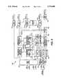
- FIG. 1Ais a block diagram illustrating a prior art computer system C incorporating DMA devices on the ISA bus;
- FIG. 1Bis a block diagram illustrating the prior art DMA controller of FIG. 1A.
- FIG. 2is a block diagram illustrating a computer system incorporating DMA devices on the PCI bus according the preferred embodiment
- FIG. 3is a more detailed block diagram illustrating the DMA master and the distributed DMA Slave controller of FIG. 2 according to the preferred embodiment.
- FIGS. 4A and 4Bare block diagrams of the distributed DMA Slave controllers of the cardbus I/F and MISC respectively.
- FIG. 5is a detailed block diagram of a distributed DMA Slave controller according to the preferred embodiment.
- FIGS. 6A and 6Bare a flow diagrams illustrating a PCI bus master read/write operation to a legacy DMA controller address as performed by the distributed DMA architecture of the present invention
- FIGS. 7A and 7Bare timing diagrams illustrating a PCI bus master write operation to a legacy DMA controller address as performed by the distributed DMA architecture of the present invention
- FIG. 8is a timing diagram illustrating a DMA operation between an I/O device and main memory according to the preferred embodiment.
- FIG. 1Athere is illustrated a computer system C of the prior art having conventional Direct Memory Access (DMA) support from an ISA bus 119.
- the computer system Cincludes a processor 100, such as a 486, Pentium® or 586 class processor coupled to a host bus 110. Also coupled to the host bus 110 are a high speed memory cache 102, a PCI/cache/memory controller 108, and a data buffer 104.
- DMADirect Memory Access
- the PCI/cache/memory controller 108is further coupled to a main memory 106 and a Peripheral Component Interface (PCI) bus 112 for controlling transfers between the processor 100/cache 102 and main memory 106; the processor 100 and the PCI bus 112; and between the PCI bus 112 and the main memory 106.
- the data buffer 104provides a data path between the processor 100/cache 102 and main memory 106; a data path between the processor 100 and the PCI bus 112; and a data path between the PCI bus 112 and the main memory 106.
- a number of PCI devicessuch as a PCI video graphics controller 114 may be coupled directly to the PCI bus 112.
- the PCI video graphics controller 114 shownprovides control and an interface to either a liquid crystal display (LCD) or cathode ray tube (CRT) monitor 120.
- a PCI/ISA bridge 117is coupled to the PCI bus 112 for providing an interface to the ISA bus 119.
- the PCI/ISA bridge 117includes conventional logic for allowing the PCI/ISA bridge 117 to perform as a PCI master or slave; a conventional ISA interface including master and slave logic and data buffers to isolate the PCI bus 112 from the ISA bus 119; and ISA support logic such as PCI and ISA arbitration logic, two 8259 compatible interrupt controllers, a 16-bit basic I/O services (BIOS) timer, three programmable timers/counters and non-maskable (NMI) control logic; and two cascaded 8237 compatible DMA controllers 202 and 204 (FIG. 1B), hereinafter referred to as a legacy DMA controller 200.
- BIOSbasic I/O services
- NMInon-maskable
- the functions provided by the PCI/ISA bridge 114are desirable in order to remain compatible with the early personal computer.
- the ISA bus 119also supports a number of standard PC peripherals, such as serial ports, parallel ports and hard disks, which are not shown here for simplicity.
- the legacy DMA controller 200provides certain ISA bus peripherals the ability to directly transfer data to or from main memory 106.
- One such peripheralis a floppy drive system, as illustrated by the floppy controller 120 coupled to a floppy drive 122.
- the floppy controller 120is coupled to a channel 2 of the DMA controllers 216 for performing the DMA transfers.
- the PCI/ISA bridge 117contains a conventional DMA controller 200, hereinafter referred to as a legacy DMA controller, which is comprised of two cascaded 8237 compatible DMA controllers 202 and 204. Each DMA controller 202 and 204 have four channels for performing DMA transfers.
- a first DMA controller (DMA1) 202handles byte-wide transfers on channels conventionally called channels 3-0.
- the first DMA controller 202is connected to a second DMA controller (DMA2) 204 in a cascaded fashion through one channel of DMA2, thereby rendering that channel unusable for DMA transfers.
- the second DMA controller 204handles wordwide transfer on channels conventionally called channels 5-7.
- the legacy DMA controller 200is coupled to an ISA bus controller 206 which also couples to the PCI bus 112 as a bridge.
- An ISA arbiter 208receives ISA bus master request signals, such as HREQ, for awarding control of the ISA bus 119.
- HREQISA bus master request signals
- the legacy DMA controller 200resides on the ISA bus 119 and the ISA cycles must be transferred through the ISA bus controller and PCI master slave 206 to get to the PCI bus 112.
- FIG. 2there is illustrated a block diagram of a computer system utilizing the present invention.
- input/output devices requiring DMA supportare coupled to the PCI bus 112 in a novel distributed DMA architecture, as disclosed herein.
- the computer systemis shown divided into a laptop portion L (hereinafter laptop computer L) and an expansion base unit portion E (hereinafter expansion base E).
- the laptop computer Lis an operationally autonomous apparatus which is detachable from the expansion base E for remote computing operations. While the laptop computer L is docked into the expansion base E, the laptop computer L operates on AC power and while the computer L is detached from the expansion base E the laptop computer L operates from battery power. Mechanisms are also provided to operate the laptop computer from AC power while removed from the expansion base E.
- the expansion base Etypically provides expandibility for functions not included in the laptop portion L.
- a processor 100is provided in the laptop computer L which is a conventional microprocessor such as an Intel Pentium or its equivalent.
- the processor 100couples to a host bus 110 for communicating with system logic such as a cache memory 102, a Mobile peripheral component interconnect bus Cache controller (MPC) 108 and pair of Mobile Data Buffers (MDB) 104.
- the cache memory 102is a conventional cache memory for the processor 100 and preferably is comprised of high speed synchronous burst static Random Access Memories (RAM).
- the MPC 108provides an interface to the cache memory 102 which includes tag RAMs and other logic for creating various cache ways, size, and speed configurations of the cache memory 102.
- the MPC 108 and the MDB 104also couple to a main memory 106 and a peripheral component interconnect (PCI) bus 112.
- PCIperipheral component interconnect
- the MPC 108provides address and control to main memory 106, which is comprised of up to 256 MByte of conventional dynamic random access memories (DRAMs).
- the MDB 104provides a 64-bit data path between the host bus 110 and the main memory 106 and provides a 32-bit data path to the PCI bus 112.
- the MPC 108 and MDB 104are proprietary devices having three major functional interfaces: a processor/cache interface, a main memory interface, and a PCI bus interface.
- the MDB 104is responsible for buffering data between the three interfaces while MPC 108 is responsible for handling addressing, command and control. Each of these interfaces operate independently from the other and include queues for read and write posting between any two of the three interfaces.
- the processor/cache interfaceallows the processor 100 to pipeline cycles into read cycles and allows snoop accesses to the tag RAM to occur while the pipeline cycles are executing.
- the memory interfacecontrols the main memory 106 and generates control signals to the MDB 104.
- the interfacealso allows read ahead operations for those PCI masters issuing a read multiple command.
- the PCI interfaceallows MPC 108 to act as a PCI master when the processor 100 is accessing the PCI bus 112, or as a PCI slave when a PCI device accesses main memory 106.
- the PCI bus 112provides a communications conduit between the laptop computer L and the expansion base E.
- a portion 112a of the PCI bus 112resides in the laptop computer L and includes a quickswitch 146 for each signal of the PCI bus 112.
- the quickswitches 146are low loss series in-line MOSFET devices with the gate connected to a docking detection means for providing hot plug capabilities.
- a portion 112b of the PCI bus 112 in the expansion base Eis coupled to the portion 112a to provide an extended PCI bus 112.
- the PCI bus 112afurther couples to a video graphics controller 114, a cardbus interface 116 (particularly 116a) and a mobile integrated system controller (MISC) 118 (particularly 116b).
- the PCI bus 112bfurther couples to a second MISC 118 (particularly 118b), two PCI slots 148, and a second cardbus interface 116 (particularly 116b).
- the video graphics controller 114further couples to a low power liquid crystal display (LCD) 120 or alternatively a cathode ray tube (CRT) style monitor.
- LCDliquid crystal display
- CRTcathode ray tube
- the cardbus interface 116includes DMA capabilities and is provided for communicating with add-on cards 120, preferably of a personal computer memory card international association (PCMCIA) style, such as networking cards, modem cards, solid state storage cards and hard disk storage cards.
- PCMCIApersonal computer memory card international association
- add-on cards 120preferably of a personal computer memory card international association (PCMCIA) style, such as networking cards, modem cards, solid state storage cards and hard disk storage cards.
- PCMCIApersonal computer memory card international association
- the DMA capabilities contained in the cardbus interface 116since, as will be discovered below, these features overcome the prior art limitations. It is noted that although the preferred embodiment includes the cardbus interface, any input/output device requiring DMA is capable of residing on the PCI bus or VL-bus according to the present invention.
- the MISC 118provides an industry standard architecture (ISA) bus 138 or 140, and an integrated drive electronics (IDE) hard drive interface for communicating with hard drives 122.
- ISAindustry standard architecture
- IDEintegrated drive electronics
- the MISC 118is configurable based on an input pin for use in both the laptop computer L, as MISC-L 118a, and expansion base E, as MISC-E 118b.
- two MISC devices, 118a and 118bare coupled to the PCI bus 112, with MISC-L 118a coupled to the PCI bus portion 112a and MISC-E 118b coupled to PCI bus portion 112b.
- MISC-Lis further coupled to the internal ISA bus 138 while MISCE is coupled to the external ISA bus 140.
- the readeris assumed to be familiar with the ISA bus.
- the MISC 118bridges the PCI bus 112 to the ISA bus 138/140 and acts as both a master and slave on the PCI bus 112 and a bus controller on the ISA buses 138 and 140.
- the MISC 118further includes a PCI bus arbiter, an ISA bus arbiter, 8237 compatible direct memory access (DMA) controllers, an enhanced DMA controller for fast IDE hard drives, 8254 compatible timers, an 8259 compatible interrupt controller, hot docking support logic, system power management logic, and plug and play support (all not shown in FIG. 2).
- DMAdirect memory access
- MISC 118Of particular interest to the present invention are the DMA controllers of MISC 118 which are more fully described below. Some components will be disabled upon initialization by software to prevent conflicts or duplication. In MISC 118 there is also a serial interrupt interface 144 for serially passing interrupts from MISC-E 118b to MISC-L 118a which provides an interrupt architecture for supporting standard ISA interrupts in a PCI based system.
- the MISC 118 and the ISA buses 138 and 140provide support for standard ISA peripherals such as those combined in a mobile super input/output (MSIO) 124 peripheral.
- the MSIO 124 peripheralis a proprietary chip having a combination of standard ISA peripherals, such as: a 146818 compatible real time clock (RTC), a floppy controller for interfacing to standard floppy drives 130; an 8051 compatible microcontroller for communicating with a standard keyboard 132 and pointing device 150, for performing scanning and key code conversions on the keyboard 132, and for performing power management functions; a universal asynchronous receiver transmitter (UART) for providing standard serial ports 136; and parallel port logic for a parallel port 134.
- RTCreal time clock
- UARTuniversal asynchronous receiver transmitter
- a read only memory (ROM) 126couples to the MSIO 124 for providing code to the 8051 microcontroller. Additionally, the ROM 126 provides basic input/output services (BIOS) code to the processor 100 which is copied from the ROM 126 and shadowed in main memory 106 upon system initialization so that thereafter the 8051 microcontroller may access the ROM 126.
- a serial bus 152is provided for communicating information relating to power management and hot docking.
- a modem and audio peripheral 128is also provided and coupled to the ISA bus 138.
- the modem and audio peripheral 128includes a standard telephony communications port for coupling to a telephone T, and an interface for coupling to a pair of stereo speakers S.
- three ISA expansion slots 142are provided for standard ISA cards.
- the cardbus interface 116includes a distributed DMA controller (DDMA) 302 which couples to the PCI bus 112 through a PCI master/slave interface 300.
- the DMA functionalityis provided by the DDMA 302 to the connected cards 120.
- the distributed DMA 302is configured according to a plurality of configuration registers 304, which are described below and are in addition to the 8237 compatible registers (not shown).
- the distributed DMA 302can perform as a PCI bus master and through the PCI master interface 300 the DDMA 302 performs DMA transfers on the PCI bus.
- Input/output cycles to the DDMA 302are handled according to a special translation method described below.
- the term distributed DMA controlleris a general term used herein to indicate DMA controllers having the capabilities of the present invention.
- Distributed DMA controllersare compatible with 8237 DMA controllers, but are independent and have the enhanced features disclosed herein. The methods disclosed herein are also applicable beyond the preferred embodiment.
- the MISC-L 118a and MISC-E 118bprovide identical features, however software may enable and disable certain features to avoid conflicts or duplication. Since the MISC-L 118a and MISC-E 118b are similar, they are described together with the differences duly noted.
- the MISC 118resides on the PCI bus 112 and performs as both a PCI slave and PCI bus master. Accordingly, a PCI master interface 310 and PCI slave interface 312 are provided for these purposes.
- the MISC 118contains a DMA controller 316 which is configurable, according to configuration registers 318, to operate as either a legacy DMA controller (legacy DMA controller 200) or a distributed DMA controller (such as DDMA 302).
- the DMA controller 316provides DMA transfers over the ISA bus as described in FIG. 1A and 1B.
- DMA controller 316is assumed to be configured as a DDMA.
- Both MISC-L 118a and MISC-E 118bhave a DMA master 314 which is coupled to the distributed DMA 316. It is the function of the DMA master 314 to translate PCI input/output cycles directed to the legacy DMA controller 200 into PCI input/output cycles recognizable by the distributed DMA's 302 and 316. Since the DMA master 314 responds to all legacy DMA controller cycles, only one of the DMA masters 314a and 314b are enabled, preferrably 314a. Thus, the DMA master 314a supports all seven channels of the legacy DMA controller 200. Accordingly, the distributed DMA 316, particularly 316b, is coupled to the PCI slave interface for receiving cycles from the DMA master 314a.
- Distributed DMA controller 316acommunicates directly with DMA master 314a and no PCI cycles are driven.
- the distributed DMA 316is also coupled to the PCI master interface 310 for performing DMA transfers over the PCI bus 112 as a bus master. It is noted that any PCI master may communicate with the input/output registers of the distributed DMA controllers 302 and 316. As such, it is contemplated that the DMA master 314 could be located in any PCI mastering device, such as the MPC 108.
- the distributed DMA controller 302is logically comprised of two DMA slave channels 400 and that the distributed DMA controller 316 is logically comprised of seven DMA slave channels 400.
- Each DMA slave channel 400compatibly functions as one channel of the legacy DMA controller 202, but each DMA slave channel being independent of each other, allows the channels to be distributed in separate PCI devices. This has the effect of breaking the legacy DMA controllers 200 into separate channels, existing in different PCI devices.
- the present inventionallows this separation, and yet to the operating system and application software there is still the appearance of the cascaded legacy DMA controllers 200.
- the DMA masterappears to software as the legacy DMA controller 200.
- each DMA slave channel 400supports certain registers of the legacy DMA controller 200, specifically, a command register 534, a status register 528, a mode register 526, a mask register 536 and a request register 538, a base address register 514, current address register 518, base word count register 516, current word count register 520, a page register 506 and a master clear register (not shown).
- the DMA slave channel 400interfaces to the PCI bus 112 through a timing and control logic block 500, a latch 540 and an I/O data buffer 504.
- the PCI interfaceis responsive as a PCI master or slave.
- the DMA slave channel 400is receiving commands from a PCI bus master, such as the processor via MPC 108 and MDB 104, the DMA slave channel is a PCI slave device.
- the DMA slave channel 400is performing DMA transfers, such as when a card 120 requests data from main memory 106, the DMA slave channel 400 is a PCI bus master device. Commands are received into the DMA slave channel 400 through the I/O data buffer 504 and decoded by a command control logic block 512.
- the memory addressis driven by the DMA slave channel 400 by the output buffer 510, the I/O buffer 508, the latch 502 and the page register 506.
- the DMA slave channel 400is not connected to the least significant address bit, so I/O buffer 508, output buffer 510 and latch 540 drive the A1-A16 address lines of the PCI address bus instead of the illustrated A0-A15 lines.
- the latch 540receives the upper 8 bits of the 16-bit address provided by the DMA slave channel 400 from the I/O data buffer 504.
- the priority encoder and rotating priority logic block 502further handles access requests to the PCI bus 112, via conventional PCI request (REQ#) and PCI grant (GNT#) signals.
- the DMA slave channel 400interfaces to the ISA peripherals, such as the floppy controller of MSIO 124, through a priority encoder 502 and the timing and control 500.
- DMA request signals(DREQ) are received into and DMA acknowledge signals (DACK) are provided from the priority encoder and rotating priority logic block 502 for resolving priority contention if more than one channel is requesting service simultaneously of the distributed DMA controller 302 or 316.
- An input/output write signal (IOW#) and input/output read signal (IOR#)are provided by the timing and control logic 500 to control DMA read and write operations with the peripheral.
- Other variations of interfacing to the peripheralsare contemplated, especially if an ISA bus is not supported and peripherals are fully contained within devices coupled to the PCI bus 112. More details on the registers described above are found in the Intel datasheets incorporated by reference.
- Each DMA slave channel 400has the above described registers in a block of 16, 8-bit registers, as defined in Table 1, to provide compatibility with the legacy DMA controller 200. However, this block is locatable anywhere in the input/output space of the laptop computer L, by programming a base address in a DMA slave configuration register, as defined in Table 2.
- the DDMA 302has two DMA slave configuration registers and DDMA's 316 have seven DMA slave configuration registers.
- Each DMA slave channelconveniently only supports one transfer size. At this point it is useful to note that although greater than seven DMA slave channels are present in the system, only seven are enabled at any one time to remain compatible.
- the DMA slave configuration registeralso contains a bit for enabling a non-legacy extended addressing mode.
- the DMA slave channel 400increases both the address registers 514 and 518; and word count registers 516 and 520 by a byte, effectively bringing the address up to 32 bits and count up to 24 bits.
- the extended address registeris located at base address +3 and extended count register at base address +6, as illustrated in Table
- the DMA master 314ais responsible for translating legacy compatible cycles into DMA slave cycles, thereby preserving compatibility via the DMA master.
- the DMA master 314ahas a DMA master configuration register (configuration registers 318a) which includes a bit for enabling the DMA master, as shown in Table 3. The default condition is disabled, whereby the legacy/distributed DMA controllers 316 would be used in the legacy configuration and legacy/distributed DMA controller 316b would be rendered unusable.
- the DMA master 314aalso contains a number of registers (configuration registers 318a) corresponding to the DMA slave configuration registers so that the DMA master may identify where each DMA slave channel 400 is located, as shown in Table 4.
- each DMA slave channel 400has a corresponding register in the DMA master 314a so that each DMA slave channel can be mapped anywhere in the input/output space of the laptop computer L.
- the 16 byte registers of all DMA slave channelscould be grouped into a single 128 byte block extending from a single base address.
- the processor 100initiates an I/O read/write cycle using compatible I/O addresses of the legacy DMA controllers 200.
- the I/O addresses for the legacy DMA controllers 200are well known in the art, but are also reproduced below in Table
- the DMA master 314arecognizing that the operation is a legacy DMA cycle, accepts the cycle. Cycles are conventionally accepted on the PCI bus 112 by driving a device select signal (DEVSEL#, not shown). As 314a is enabled and 314b is disabled, only 314a responds.
- the DMA master 314aissues a retry to the processor 100 to force the processor 100, or actually the PCI/cache/memory controller 108, off the PCI bus 112. Cycles are conventionally retried with a STOP# signal, and particular timing depends upon whether or not data is accepted.
- the DMA master 314arequests the PCI bus 112.
- the DMA master 314awaits for the PCI bus 112 to be granted.
- the DMA master 314adetermines which of the DMA slave channels 400 are targeted and thereafter reads/writes to the individual DMA slave channels registers, as shown in step 608.
- the DMA master 314awill perform up to four read/writes to the DMA slave channels 400, corresponding to the four byte-wide or three word-wide channels. If the DMA master 314a is reading from individual DMA slave channels 400, such as the status register 528, the data is merged into a single byte to provide a compatible response to the processor.
- the number of write cyclesis dependant upon which channels are effected by the write cycle. For example, a new command register value for DMA1 202 will be written to all the DMA slave channels 400 corresponding to the byte-wide channels 3-0, whereas a new mask register value will only be written to one of the DMA slave channels. Further details on the construction and decoding of legacy DMA controller registers is contained below in the DMA control register descriptions.
- the DMA master 314ais controlled by the processor 100, and the DMA slave channels 400 are slaved to the DMA master 314a. It is the responsibility of each DMA slave channel 400 to respond and terminate a PCI I/O read/write to its registers. Hence, each register of each individual DMA slave channel 400 is addressable according to the address maps of Tables 6-14. The bit descriptions and positions for each register are compatible with the 8237 unless otherwise noted.
- the DMA master 314asets an internal completion flag to indicate completion.
- the DMA master 314athen relinquishes control of the PCI bus 112, by deasserting the request signal (REQI), as shown at step 612.
- the DMA master 314awaits for the processor 100 to retry the legacy DMA I/O read/write cycle.
- the DMA master 314anow having completed its communications with the individual DMA slave channels 400, thereby responds to this second request.
- the requestwas a read directed to the legacy DMA controller 200, then the data is provided. If the request was a write operation directed to a legacy DMA controller 200, then a completion indication is provided, the write data having actually been sampled on the first attempt. When responding, the DMA master 314a resets the completion flag. Thereby, compatibility to the legacy DMA controllers 200 is achieved through the master/slave method disclosed above. It is contemplated that this method is useful for other applications requiring compatibility or isolation.
- the DMA master 314asupports the programming model of the legacy DMA controller 200 through a plurality of control registers, described below in Tables 6-14. Since there are both byte-wide and word-wide DMA controllers in the laptop computer L, there are two registers for each register defined. Also, since the DMA master 314a translates legacy cycles to DMA slave cycles, two sets of input/output addresses are defined.
- FIG. 6Bthere is illustrated an alternative method of accessing the DMA slaves 302 and 316.
- FIG. 6Bcorresponds to an alternative embodiment, mentioned above, in which the DMA master 314 would be contained in MPC 108 and MDB 104 (MPC/MDB).
- the processor 100would provide the access cycle to the MPC/MDB using the legacy addresses, as shown at step 620.
- the MPC/MDBreceives the cycle and before passing the cycle to the PCI bus 112, the MPC/MDC translates the cycle into at least one bus transaction directed to one of the individual DMA slave channel 400 registers at its corresponding address.
- the MPC/MDBrequests access to the PCI according to PCI conventions, as shown at steps 624 and 626.
- the MPC/MDBaccesses the request register.
- the number of bus transactionsis dependant upon whether the cycle is a read or a write, and which register is being accessed. Details on the suggested number of cycles are contained below in Tables 6-14.
- Each DMA slave channel 400 being accessedprovides a response to MPC/MDB. The response is similar to that described steps 608 and 610 of FIG. 6A.
- the MPC/MDBprovides the received responses to the processor 100.
- the retry operationis not needed since the DMA master is placed between the processor 100 and the DMA slave channels 400. It is useful to note, however, that if another PCI master requests access to the DMA channel slaves 400 by using a legacy address, a retry operation, such as described in FIG. 6A would be necessary.
- FIGS. 7A and 7Ba write transaction directed to the command register of the byte-wide legacy DMA controller 202 is illustrated.
- the command registeris a shared register and that the byte-wide DMA controller functionality may be distributed among up to four DMA slave channels 400
- the single write transaction directed to the legacy DMA controller 202 addressmay result in up to four write transactions to the DMA slave channels 400.
- channel 0has been assigned to the distributed DMA controller 302 with one of the two DMA slave channels 400 being having the assignment.
- DMA channels 1-3are assumed disabled for simplicity.
- any PCI bus mastermay direct read/write cycles to the legacy DMA controllers 200 with similar results.
- the preferred embodimentprovides the DMA master 314a in the MISC 118, an alternative is to place the DMA master closer to the processor 100, such as in the MPC 108/MDB 104.
- the processor 100causes a processor PCI bus access request (PREQ#) signal to be asserted, intending to write a value into the command register of the byte-wide legacy DMA controller 202.
- PREQ#processor PCI bus access request
- the arbiter of the MISC-L 118provides a grant (PGNT#) signal to the processor 100 to indicate that the processor has been granted access to the PCI bus 112.
- PGNT#grant
- a frame (FRAME#) signalis asserted to indicated the beginning of a transaction, as shown at clock 3.
- the processor 100causes an address to be placed on an address/data portion of the PCI bus 112 and a PCI command to be placed on a command/byte enable portion of the PCI bus 112.
- the address 0008hindicates the input/output address of the legacy DMA controller 202 command register.
- the PCI commandindicates that the operation is a I/O write operation.
- the FRAME# signalis deasserted since only one data phase is needed.
- the initiator ready (IRDY#)is asserted by the processor 100 to indicate that data is available to be written.
- DMA master 314aonly DMA master 314a responds to legacy DMA addresses when configured in distributed DMA configuration.
- the DMA mastermay need to communicate with the DDMA controllers before the transaction can be successfully completed. This is especially true where the processor is requesting a certain channel register to be read. Therefore, at clock 5 the DMA master 314a asserts a device select (DEVSEL#) signal to claim the transaction and asserts a stop (STOP#) signal to terminate the transaction and cause it to be retried. Although the transaction is terminated, if the transaction is a write transaction, the DMA master 314a latches the data at clock 6.
- DEVSEL#device select
- STOP#stop
- the processorsince IRDY# and STOP# are asserted, the processor must cause the PREQ# signal to be deasserted for at least two clock cycles so that another device may have access to the PCI bus 112. At clock 7 the PGNT# is deasserted following the deasserted PREQ# signal.
- the DMA master 314arequests access to the PCI bus 112 by asserting its request (MDMAREQ#) signal. Sometime later, the arbiter of MISC-L 118a will provide a grant (MDMAGNT#) signal to the DMA master 314a, as shown in clock 8.
- the DMA master 314abegins to process the requested write transaction.
- the DMA master 314aprovides an address, for example 1008h, and PCI bus command and causes the FRAME# signal to be asserted.
- the I/O addressis 1008h to indicate the command register associated with channel 0. Since DMA slave channel 400a of distributed DMA controller 302 has been configured for channel 0, it is the only distributed DMA controller that will respond to this address.
- the distributed DMA controllers 302 and 316only respond to the addresses associated with channels they have been configured for. While a particular DMA slave channel knows its addresses, it is not necessary for it to know which channel number it is.
- the DMA master 314aprovides the write data received from the processor 100 to the DMA slave channel 400a.
- the byte enable (BE) signalsindicate that only one byte is present.
- the initiator ready (IRDY#) signalis provided by the DMA master 314a to indicate that the data is available.
- the DMA slave channel 400aclaims the transaction by asserting the device select (DEVSEL#) signal and accepts the data by asserting the target ready (TRDY#) signal.
- the write datais latched into the DMA slave channel command register at clock 12 and the transaction is completed.
- the processor 100reacquires the PCI bus 112 when the PGNT# signal is asserted.
- the cycle of clocks 2-4are retried, as shown in clocks 15-17.
- the completion flagwill be set. This causes the DMA master 314a to claim the cycle, by asserting the DEVSEL# signal, and complete the cycle, by asserting the TRDY# signal. If the cycle is a read, data will be provided to the processor 100. If the cycle is a write, the cycle will terminate successfully indicating to the processor that the write cycle was performed.
- the processorperforms cycles directed to the legacy DMA controllers 200, according to conventional operating system software, and the DMA master 314a hides the distributed DMA architecture, thereby appearing as the compatible legacy DMA controllers 200.
- FIG. 8a typical DMA data transfer according to the preferred embodiment is illustrated.
- This exampleillustrates the timing between the DMA slave channel 400, the PCI bus 112, the target PCI device (main memory 106) and the DMA peripheral.
- the DMA peripheralis assumed to be a card 120, such as a network card requiring DMA transfers.
- the data transferis from the network card 120, in conjunction with distributed DMA controller 302, to the main memory 106, such as when the computer has requested data from the network.
- the laptop computer Lhas requested the network card 120 to obtain certain data from the network (not shown).
- the laptop computer Linstructs the network card 120 to provide the data via a DMA operation.
- the computeralso initializes the DMA controllers to prepare for the transfer.
- the DMA master 314areceives the command and initializes DMA slave channel 400, according to the methods described above.
- FIG. 8illustrates a number of signals referenced to a PCI clock (PCICLK) signal.
- PCICLKPCI clock
- the PCICLKis provided for illustration purposes only. Signals specific to the PCI bus are properly referenced to the PCICLK signal, but other signals, such as the DMA signals may be dependent on a different clock signal. Further, it is noted that design choices may vary the response time of certain signals, but the sequence of signals is generally as shown.
- a DMA request (DREQ) signalis asserted, as shown at clock 1.
- the DREQ signalis received by the DMA slave channel 400a and in response the DMA slave channel requests access to the PCI bus 112 by asserting a PCI bus request (REQ#) signal, as shown at clock 2.
- the PCI bus arbiter of MISC 118aprovides a bus grant (GNT#) signal to the DMA slave channel 400a at a time when the bus is available, as shown at clock 3.
- the DMA slave channel 400athen provides a DMA acknowledge (DACK) signal to the network card 120 to indicate bus availability.
- DACKDMA acknowledge
- the DMA slave channel 400adrives a memory address and PCI bus command onto the PCI bus 112.
- the memory addressindicates where the transferred data is to be written into the main memory 106.
- the PCI bus commandindicates that a memory write operation is occurring on the PCI bus.
- the DMA slave channel 400adrives a frame (FRAME#) signal to indicate the validity of these values and to initiate the PCI bus operation, as shown at clock 5.
- the DREQ signalis deasserted shortly after the DACK signal is asserted. If more than one byte was to be transferred, the DREQ signal would remain asserted until during the last byte transfer. It is noted that a DMA operation may also be terminated when a terminal count is reached. More details are found in the Intel datasheets incorporated by reference. When the DREQ signal is deasserted, the REQ# and GNT# signals are also deasserted according to PCI bus specification convention.
- the main memory 106decodes the address and claims the operation by asserting a device select (DEVSEL#) signal, as shown at clock 6. If the main memory 106 is ready to receive the data, the main memory 106 provides a target ready (TRDY#) signal to indicate readiness, as shown at clock 6. According to the PCI bus specification, both the TRDY# signal and an initiator ready (IRDY#) signal must be asserted before the transaction is ended. In this example, IRDY# is not asserted yet.
- the DMA slave channel 400adoes not provide an input/output read (IOR#) signal until the DMA slave channel 400a has tri-stated the bus, as shown at clock 6.
- IOR#input/output read
- the IOR# signalis provided to the network card 120 to indicate that data may be provided onto an address/data portion of the PCI bus.
- datais provided from the network card 120.
- the DMA slave channel 400aprovides the byte enable (C/BE#) signals to the PCI bus 112 to indicate that a single byte is provided on a lower eight bits of the PCI address/data bus.
- the DMA slave channel 400aknowing the data valid timing of the network card 120, drives the IRDY# signal at clock 7 to indicate data availability to the main memory 106. At clock 8, the DACK, IRDY#, TRDY#, DEVSEL# and IORI signals are deasserted as the transfer is complete.
- the peripheralscan be directly coupled to the PCI without sideband signals and without requiring an ISA bus.
- the DMA master 314ahandles write cycles to the legacy address of the command register in the special way described above. Four I/O writes are performed if the write cycle is to the byte legacy DMA controller 202 and three I/O writes are performed if the write is to the word DMA legacy controller 204. For the DMA channels 400, the function of this register is the same as for the legacy DMA controllers 200.
- Data bits 0 and 1 of the legacy DMA address of the mode registerindicate which legacy channel to apply the other six bits.
- the DMA master 314auses these bits to determine which DMA slave channel 400 will receive this data.
- the DMA master 314ahandles writes to this legacy address in the same special way described above.
- data bits 0 and 1are considered reserved and are written "undefined" by the DMA master 314a.
- the functionality of the remainder of this registeris identical to the legacy DMA controller 200 when applicable.
- Data bits 0 and 1 of the legacy DMA address of the request registerindicate which legacy channel to apply the other six bits.
- the DMA master 314auses these bits to determine which DMA slave channel 400 will receive the data.
- the DMA master 314ahandles writes to this legacy address in the same special way described above.
- data bits 0 and 1are considered reserved and are written "undefined" by the DMA master 314a.
- the functionality of the remainder of this registeris identical to the legacy DMA controller 200 when applicable.
- Data bits 0 and 1 of the legacy DMA address of the single channel mask registerindicate which legacy channel to apply the other bit.
- the DMA master 314auses these bits to determine which DMA slave channel 400 will receive this data.
- the DMA master 314ahandles writes to this legacy address in the same special way described above.
- each DMA slave channel 400does not have a corresponding single channel mask register.
- a write to this legacy addresscauses the DMA master 314a to write to the multi-channel mask register (described below) in the targeted DMA slave channel 400, with bit 0 carrying the new mask status.
- Data bit positions 0-3 of the legacy DMA address to the multi channel mask registerindicate the legacy channels to apply the data to.
- the DMA master 314auses these bit positions to determine the DMA slave channels 400 will receive this data.
- the DMA master devicehandles writes to this legacy address in the same special way described above. There are four I/O slave writes if the legacy address is to the byte DMA the byte legacy DMA controller 202, and there are three I/O slave writes if the legacy address is to the word legacy DMA controller 204.
- the master DMA 314ahandles reads to the legacy address of the status register in the same special way described above. There are four I/O slave reads if the legacy address is to the byte legacy DMA controller 202, and there are three I/O slave reads if the legacy address is to the word legacy DMA controller 204. It is the DMA master's responsibility to properly assemble the contents of this register. To facilitate assembly, each DMA slave channel returns the same TC indication on bits 0-3 in the same channel request indication on bits 4-7.
- a write to this legacy addressclears the first, last flip-flop.
- the write datais irrelevant.
- the DMA master 314ahandles a write to this legacy address, and keeps track of the state of this flip-flop. Thus, the DMA slave 400 does not require the flip-flop.
- a write to this legacy addressperforms the same function as a hardware reset. The data written is irrelevant.
- the DMA master 314ahandles writes to this legacy address in the same special way described above. There are four I/O slave writes if the legacy address is to the byte legacy DMA controller 202 and there are three I/O slave writes if the legacy address is to the word legacy DMA controller 204.
- a write to this legacy addresscauses the DMA master 314a to write to the multi-channel mask registers (described above) of the corresponding DMA slave channels 400, with bit 0 set to 0.
- the act of writing this addressenables all four byte DMA channels or all three word DMA slave channels to accept DMA requests. The data written is irrelevant.
- the DMA master 314ahandles a write to this register in the same special way described above.
- the DMA master 314awill respond to and terminate a PCI I/O write to the legacy address of the temporary register and drives the bits "undefined".
Landscapes
- Engineering & Computer Science (AREA)
- Theoretical Computer Science (AREA)
- Physics & Mathematics (AREA)
- General Engineering & Computer Science (AREA)
- General Physics & Mathematics (AREA)
- Computer Hardware Design (AREA)
- Microelectronics & Electronic Packaging (AREA)
- Bus Control (AREA)
Abstract
Description
TABLE 1 ______________________________________ DMA Slave Channel registers Slave address R/W Register Name ______________________________________ base + 0h W Base Address 0-7 base + 0h R Current Address 0-7 base + 1h W Base Address 8-15 base + 1h R Current Address 8-15 base + 2h W Base Address 16-23 base + 2h R Current Address 16-23 base + 3h W Base Address 24-31 base + 3h R Current Address 24-31 base + 4h W Base Word Count 0-7 base + 4h R Current Word Count 0-7 base + 5h W Base Word Count 8-15 base + 5h R Current Word Count 8-15 base + 6h W Base Word Count 16-23 base + 6h R Current Word Count 16-23 base + 7h N/A Reserved base + 8h W Command base + 8h R Status base + 9h W Request base + Ah N/A Reserved base + Bh W Mode base + Ch W Reserved base + Dh W Master Clear base + Eh N/A Reserved base + Fh R/W Multi-Channel Mask ______________________________________
TABLE 2 ______________________________________ DMA Slave Configuration register Bits Description ______________________________________ 0-0Channel Enable 0 disabled 1 enabled 1-2 Transfer Size 00 = 8 bit transfer 01 = 16bit transfer 10 = 32 bit transfer, non Legacy 11 = reserved 3 Non Legacy ExtendedAddress 0 = disabled 1 = enabled 4-15 Slave Base Address 15-4 ______________________________________
TABLE 3 ______________________________________ DMA Master Configuration Register Bits Description ______________________________________ 31 Master DMA Enabled 0 disabled 1 enabled 30-8 RESERVED always reads 0's 7-5 Identifies active DMA channel in MISC PCI device. One bit per channel. 0 DistributedLegacy DMA Channel 1 LocalLegacy DMA Channel 4 RESERVED always reads 0's 3-0 Identifies active DMA channel in MISC PCI device. One bit per channel. 0 DistributedLegacy DMA Channel 1 Local Legacy DMA Channel ______________________________________
TABLE 4 ______________________________________ DMA Slave Configuration Registers Bits Read/Write Description ______________________________________ 31-19 R RESERVED always return's 0's 15-7 W/R Slave Base Address where the 16 byte block of programming register for this channel exist 6-4 R 001 - DMA Channel 1 Slave Lower Address (6-4) Defines the start of the 16 byte block of I/O addresses for Channel 1 010 - DMA Channel 2 Slave Lower Address (6-4) Defines the start of the 16 byte block of I/O addresses for Channel 2 011 - DMA Channel 3 Slave Lower Address (6-4) Defines the start of the 16 byte block of I/O addresses for Channel 3 101 - DMA Channel 5 Slave Lower Address (6-4) Defines the start of the 16 byte block of I/O addresses for Channel 5 110 - DMA Channel 6 Slave Lower Address (6-4) Defines the start of the 16 byte block of I/O addresses for Channel 6 111 - DMA Channel 7 Slave Lower Address (6-4) Defines the start of the 16 byte block of I/O addresses for Channel 7 3 W/R Non Legacy Extended Addressing RESERVED always return's O'sO = enabled 1 = enabled 2-1 W/R Transfer Size 00 = 8 bit transfer 01 = 16 bit transfer 10 = RESERVED 11 = RESERVED 0 R Channel slave interface active bit. When set to a 1, the distributed DMA Slave will accept PCI cycles to the programmed address in bits 4-15 (Dual port register with the DMA Master Configuration Register) ______________________________________
TABLE 5 ______________________________________ LEGACY DMA I/O ADDRESS I/O ADDRESS RANGE FUNCTION ______________________________________ 000 - 01F DMA Controller 202d (byte transfers) 080 - 08F DMA PAGE REGISTERS 0CD - 0DF DMA CONTROLLER 202c (word transfers) 08O - 08F Extended Page Registers ______________________________________
TABLE 6 ______________________________________ Command Register I/O Byte Legacy 0008h address Device Address Slave Base + 8h Address Word Legacy 00D0h Device Address Slave Base +3h Address Size 8 bits Type Write only Power up 00000000b ______________________________________
TABLE 7 ______________________________________ Mode Register I/O Byte Legacy 000Bh address Device Address Slave Base + Bh Address Word Legacy 00D6h Device Address Slave Base +Bh Address Size 8 bits Type Write only Power up 00000000b ______________________________________ Mode Register ______________________________________ 0-1 Slave - reserved, Master - Channel select 000 or 4 01 Channel 1 or 5 10 Channel Channel 2 or 6 113 or 7 2-7 See Intel 8237 data sheets ______________________________________ Channel
TABLE 8 ______________________________________ Request Register I/O Byte Legacy 0009h address Device Address Slave Base + 9h Address Word Legacy 00D2h Device Address Slave Base +9h Address Size 8 bits Type Write only Power up 00000000b ______________________________________ Request Register Bits Description ______________________________________ 0-1 Slave - reserved, Master - Channel select 000 or 4 01 Channel 1 or 5 10 Channel Channel 2 or 6 113 or 7 2-7 Not described ______________________________________ Channel
TABLE 9 ______________________________________ Single Channel Mask Register I/O Byte Legacy 000Ah address Device Address Slave Base + Fh Address Word Legacy 00D4h Device Address Slave Base +Fh Address Size 8 bits Type Write only Power up 00000000b ______________________________________ Single Channel Mask Register Bits Description ______________________________________ 0-1 Slave - reserved, Master - Channel select 000 or 4 01 Channel 1 or 5 10 Channel Channel 2 or 6 113 or 7 2-7 Not described ______________________________________ Channel
TABLE 10 ______________________________________ Multi-Channel Mask Register I/O Byte Legacy 000Fh address Device Address Slave Base + Fh Address Word Legacy 00DEh Device Address Slave Base +Fh Address Size 8 bits Type Write/Read Power up 00000001b ______________________________________ Multi- Channel Mask Register Bits Description ______________________________________ 0 Slave - Mask bit select, Legacy -0 or 4 Mask bit select 0 channel Clear mask bit 1Set mask bit 1 Slave - reserved, Legacy -1 or 5 Mask bit select 0 Channel Clear mask bit 1 Set mask bit 2 Slave - reserved, Legacy -Channel 2 or 6 Mask bit select 0Clear mask bit 1Set mask bit 3 Slave - reserved, Legacy -3 or 7 Mask bit select 0 Channel Clear mask bit 1 Set mask bit 4-7 Don't Care ______________________________________
TABLE 11 ______________________________________ Status Register I/O Byte Legacy 0008h address Device Address Slave Base + 8h Address Word Legacy 00D0h Device Address Slave Base +8h Address Size 8 bits Type Read only Power up XXXX0000b ______________________________________ Status Register Bits Description ______________________________________ 0 Slave - TC indication; Legacy -0 or 4 Channel TC indication 0 TC has not been reached 1 TC has been reached 1 Slave - TC indication, Legacy -1 or 5 Channel TC indication 0 TC has not been reached 1 TC has been reached 2 Slave - TC indication, Legacy -Channel 2 or 6TC indication 0 TC has not been reached 1 TC has been reached 3 Slave - TC indication, Legacy -3 or 7 Channel TC indication 0 TC has not been reached 1 TC has been reached 4 Slave - Channel request, Legacy -0 or 4 Channel request 0 Norequest 1Channel request 5 Slave - Channel request, Legacy -1 or 5 Channel request 0 Norequest 1Channel request 6 Slave - Channel request, Legacy -Channel 2 or 6request 0 Norequest 1Channel request 7 Slave - Channel request, Legacy -3 or 7 Channel request 0 Norequest 1 Channel request ______________________________________
TABLE 12 ______________________________________ Clear First/Last Flip-Flop I/O Byte Legacy 000Ch address Device Address Slave N/A Address Word Legacy 00D8h Device Address Slave N/A Address Size 1 bit Type Write only Power up Xb ______________________________________
TABLE 13 ______________________________________ Master Clear I/O Byte Legacy 000Dh address Device Address Slave Base + Dh Address Word Legacy 00DAh Device Address Slave Base +Dh Address Size 0 bits Type Write only Power up N/A ______________________________________
TABLE 14 ______________________________________ Clear Mask Register I/O Byte Device Legacy 000Eh address Address Slave Base + Fh Address Word Device Legacy 00DCh Address Slave Base +Fh Address Size 0 bits Type Write only Power up N/A ______________________________________
Claims (65)
Priority Applications (8)
| Application Number | Priority Date | Filing Date | Title |
|---|---|---|---|
| US08/570,394US5774680A (en) | 1995-12-11 | 1995-12-11 | Interfacing direct memory access devices to a non-ISA bus |
| US08/639,879US5838993A (en) | 1995-12-11 | 1996-04-26 | System for DMA controller sharing control signals in conventional mode and having separate control signals for each number of channels in distributed mode |
| US08/639,881US5765024A (en) | 1995-12-11 | 1996-04-26 | System for requesting access to DMA channel having address not in DMA registers by replacing address of DMA register with address of requested DMA channel |
| EP96308940AEP0784277B1 (en) | 1995-12-11 | 1996-12-10 | Interfacing direct memory access devices to a non-ISA bus |
| DE69626485TDE69626485T2 (en) | 1995-12-11 | 1996-12-10 | Interface formation between direct memory access device and a non-ISA bus |
| TW085115332ATW379294B (en) | 1995-12-11 | 1996-12-11 | Interfacing direct memory access devices to a non-isa bus |
| US08/950,297US6088517A (en) | 1995-12-11 | 1997-10-14 | Interfacing direct memory access devices to a non-ISA bus |
| US09/094,218US5875351A (en) | 1995-12-11 | 1998-06-09 | System for requesting access to DMA channel having address not in DMA registers by replacing address of DMA register with address of requested DMA channel |
Applications Claiming Priority (1)
| Application Number | Priority Date | Filing Date | Title |
|---|---|---|---|
| US08/570,394US5774680A (en) | 1995-12-11 | 1995-12-11 | Interfacing direct memory access devices to a non-ISA bus |
Related Child Applications (4)
| Application Number | Title | Priority Date | Filing Date |
|---|---|---|---|
| US08/639,879Continuation-In-PartUS5838993A (en) | 1995-12-11 | 1996-04-26 | System for DMA controller sharing control signals in conventional mode and having separate control signals for each number of channels in distributed mode |
| US08/639,881Continuation-In-PartUS5765024A (en) | 1995-12-11 | 1996-04-26 | System for requesting access to DMA channel having address not in DMA registers by replacing address of DMA register with address of requested DMA channel |
| US08/639,881ContinuationUS5765024A (en) | 1995-12-11 | 1996-04-26 | System for requesting access to DMA channel having address not in DMA registers by replacing address of DMA register with address of requested DMA channel |
| US08/950,297ContinuationUS6088517A (en) | 1995-12-11 | 1997-10-14 | Interfacing direct memory access devices to a non-ISA bus |
Publications (1)
| Publication Number | Publication Date |
|---|---|
| US5774680Atrue US5774680A (en) | 1998-06-30 |
Family
ID=24279478
Family Applications (5)
| Application Number | Title | Priority Date | Filing Date |
|---|---|---|---|
| US08/570,394Expired - LifetimeUS5774680A (en) | 1995-12-11 | 1995-12-11 | Interfacing direct memory access devices to a non-ISA bus |
| US08/639,879Expired - LifetimeUS5838993A (en) | 1995-12-11 | 1996-04-26 | System for DMA controller sharing control signals in conventional mode and having separate control signals for each number of channels in distributed mode |
| US08/639,881Expired - LifetimeUS5765024A (en) | 1995-12-11 | 1996-04-26 | System for requesting access to DMA channel having address not in DMA registers by replacing address of DMA register with address of requested DMA channel |
| US08/950,297Expired - LifetimeUS6088517A (en) | 1995-12-11 | 1997-10-14 | Interfacing direct memory access devices to a non-ISA bus |
| US09/094,218Expired - LifetimeUS5875351A (en) | 1995-12-11 | 1998-06-09 | System for requesting access to DMA channel having address not in DMA registers by replacing address of DMA register with address of requested DMA channel |
Family Applications After (4)
| Application Number | Title | Priority Date | Filing Date |
|---|---|---|---|
| US08/639,879Expired - LifetimeUS5838993A (en) | 1995-12-11 | 1996-04-26 | System for DMA controller sharing control signals in conventional mode and having separate control signals for each number of channels in distributed mode |
| US08/639,881Expired - LifetimeUS5765024A (en) | 1995-12-11 | 1996-04-26 | System for requesting access to DMA channel having address not in DMA registers by replacing address of DMA register with address of requested DMA channel |
| US08/950,297Expired - LifetimeUS6088517A (en) | 1995-12-11 | 1997-10-14 | Interfacing direct memory access devices to a non-ISA bus |
| US09/094,218Expired - LifetimeUS5875351A (en) | 1995-12-11 | 1998-06-09 | System for requesting access to DMA channel having address not in DMA registers by replacing address of DMA register with address of requested DMA channel |
Country Status (4)
| Country | Link |
|---|---|
| US (5) | US5774680A (en) |
| EP (1) | EP0784277B1 (en) |
| DE (1) | DE69626485T2 (en) |
| TW (1) | TW379294B (en) |
Cited By (25)
| Publication number | Priority date | Publication date | Assignee | Title |
|---|---|---|---|---|
| US5918028A (en)* | 1997-07-08 | 1999-06-29 | Motorola, Inc. | Apparatus and method for smart host bus adapter for personal computer cards |
| US5954802A (en)* | 1996-01-31 | 1999-09-21 | Texas Instruments Incorporated | System for interfacing ISA compatible computer devices with non-ISA buses using secondary DMA controllers and glue logic circuit |
| US6256692B1 (en)* | 1997-10-13 | 2001-07-03 | Fujitsu Limited | CardBus interface circuit, and a CardBus PC having the same |
| US6510484B1 (en) | 1998-06-30 | 2003-01-21 | Samsung Electronics Co., Ltd. | Technique for controlling synchronous devices and asynchronous devices connected to an inter-integrated circuit bus (I2C bus) |
| US6571302B1 (en) | 2000-04-04 | 2003-05-27 | Advanced Digital Information Corporation | Dynamic adjustment of multiple sequential burst data transfers |
| US6598104B1 (en)* | 1998-01-07 | 2003-07-22 | Koninklijke Philips Electronics N.V. | Smart retry system that reduces wasted bus transactions associated with master retries |
| US6606690B2 (en) | 2001-02-20 | 2003-08-12 | Hewlett-Packard Development Company, L.P. | System and method for accessing a storage area network as network attached storage |
| US20040059862A1 (en)* | 2002-09-24 | 2004-03-25 | I-Bus Corporation | Method and apparatus for providing redundant bus control |
| US6804819B1 (en) | 2000-09-18 | 2004-10-12 | Hewlett-Packard Development Company, L.P. | Method, system, and computer program product for a data propagation platform and applications of same |
| US20040225785A1 (en)* | 2001-03-22 | 2004-11-11 | I-Bus/Phoenix, Inc. | Hybrid switching architecture |
| US20050089311A1 (en)* | 2003-10-22 | 2005-04-28 | Ming-Hou Dai | Computer system having direct media access mode |
| US6977927B1 (en) | 2000-09-18 | 2005-12-20 | Hewlett-Packard Development Company, L.P. | Method and system of allocating storage resources in a storage area network |
| US20080059670A1 (en)* | 2006-09-01 | 2008-03-06 | Via Technologies, Inc. | Control method and system of constructing raid configuration across multiple host bus adapters |
| US7386610B1 (en) | 2000-09-18 | 2008-06-10 | Hewlett-Packard Development Company, L.P. | Internet protocol data mirroring |
| US20130290579A1 (en)* | 2012-04-27 | 2013-10-31 | Ming-Cheng Lin | Pci-based interfacing device with mappable port addresses to legacy i/o port addresses |
| US20170177520A1 (en)* | 2015-12-22 | 2017-06-22 | Futurewei Technologies, Inc. | System and Method for Efficient Cross-Controller Request Handling in Active/Active Storage Systems |
| US10983942B1 (en) | 2019-12-11 | 2021-04-20 | Qorvo Us, Inc. | Multi-master hybrid bus apparatus |
| US11106615B2 (en) | 2019-01-16 | 2021-08-31 | Qorvo Us, Inc. | Single-wire bus (SuBUS) slave circuit and related apparatus |
| US11119958B2 (en)* | 2019-04-18 | 2021-09-14 | Qorvo Us, Inc. | Hybrid bus apparatus |
| US11226924B2 (en) | 2019-04-24 | 2022-01-18 | Qorvo Us, Inc. | Single-wire bus apparatus supporting slave-initiated operation in a master circuit |
| US11409677B2 (en) | 2020-11-11 | 2022-08-09 | Qorvo Us, Inc. | Bus slave circuit and related single-wire bus apparatus |
| US11489695B2 (en) | 2020-11-24 | 2022-11-01 | Qorvo Us, Inc. | Full-duplex communications over a single-wire bus |
| US11706048B1 (en) | 2021-12-16 | 2023-07-18 | Qorvo Us, Inc. | Multi-protocol bus circuit |
| US12092689B2 (en) | 2021-12-08 | 2024-09-17 | Qorvo Us, Inc. | Scan test in a single-wire bus circuit |
| US12182052B2 (en) | 2022-01-20 | 2024-12-31 | Qorvo Us, Inc. | Slave-initiated communications over a single-wire bus |
Families Citing this family (102)
| Publication number | Priority date | Publication date | Assignee | Title |
|---|---|---|---|---|
| JP3403284B2 (en)* | 1995-12-14 | 2003-05-06 | インターナショナル・ビジネス・マシーンズ・コーポレーション | Information processing system and control method thereof |
| US6233704B1 (en)* | 1996-03-13 | 2001-05-15 | Silicon Graphics, Inc. | System and method for fault-tolerant transmission of data within a dual ring network |
| JPH1040211A (en)* | 1996-04-30 | 1998-02-13 | Texas Instr Inc <Ti> | Method for directly assigning memory access priority in packeted data communication interface equipment and dma channel circuit |
| US5991841A (en)* | 1997-09-24 | 1999-11-23 | Intel Corporation | Memory transactions on a low pin count bus |
| US6119189A (en)* | 1997-09-24 | 2000-09-12 | Intel Corporation | Bus master transactions on a low pin count bus |
| US6157970A (en)* | 1997-09-24 | 2000-12-05 | Intel Corporation | Direct memory access system using time-multiplexing for transferring address, data, and control and a separate control line for serially transmitting encoded DMA channel number |
| US5938744A (en)* | 1997-11-04 | 1999-08-17 | Aiwa/Raid Technlogy, | Method for managing multiple DMA queues by a single controller |
| US6230219B1 (en)* | 1997-11-10 | 2001-05-08 | International Business Machines Corporation | High performance multichannel DMA controller for a PCI host bridge with a built-in cache |
| US5983024A (en)* | 1997-11-26 | 1999-11-09 | Honeywell, Inc. | Method and apparatus for robust data broadcast on a peripheral component interconnect bus |
| KR19990043773A (en)* | 1997-11-29 | 1999-06-15 | 정선종 | Direct memory access controller |
| US6353866B1 (en) | 1998-01-07 | 2002-03-05 | National Semiconductor Corporation | Apparatus and method for initializing a universal serial bus device |
| US6205501B1 (en) | 1998-01-07 | 2001-03-20 | National Semiconductor Corp. | Apparatus and method for handling universal serial bus control transfers |
| US6157975A (en)* | 1998-01-07 | 2000-12-05 | National Semiconductor Corporation | Apparatus and method for providing an interface to a compound Universal Serial Bus controller |
| US6070208A (en)* | 1998-01-07 | 2000-05-30 | National Semiconductor Corporation | Apparatus and method for implementing a versatile USB endpoint pipe |
| US6122676A (en)* | 1998-01-07 | 2000-09-19 | National Semiconductor Corporation | Apparatus and method for transmitting and receiving data into and out of a universal serial bus device |
| US6412027B1 (en)* | 1998-02-11 | 2002-06-25 | Globespanvirata, Inc. | Direct memory access controller having on-board arbitration circuitry |
| US6122679A (en)* | 1998-03-13 | 2000-09-19 | Compaq Computer Corporation | Master DMA controller with re-map engine for only spawning programming cycles to slave DMA controllers which do not match current programming cycle |
| US6473780B1 (en)* | 1998-04-01 | 2002-10-29 | Intel Corporation | Scheduling of direct memory access |
| US6138183A (en)* | 1998-05-06 | 2000-10-24 | Ess Technolgoy Inc. | Transparent direct memory access |
| US5966384A (en)* | 1998-05-08 | 1999-10-12 | Motorola, Inc. | Method and apparatus for data transmission within a broad-band communication system |
| JP2938049B1 (en)* | 1998-07-02 | 1999-08-23 | 新潟日本電気株式会社 | A control device for hot-swapping an expansion I/O device into a computer main unit |
| US7158532B2 (en)* | 1998-07-06 | 2007-01-02 | Intel Corporation | Half duplex link with isochronous and asynchronous arbitration |
| US6163818A (en)* | 1998-08-27 | 2000-12-19 | Xerox Corporation | Streaming memory controller for a PCI bus |
| US6425021B1 (en)* | 1998-11-16 | 2002-07-23 | Lsi Logic Corporation | System for transferring data packets of different context utilizing single interface and concurrently processing data packets of different contexts |
| US6260082B1 (en)* | 1998-12-23 | 2001-07-10 | Bops, Inc. | Methods and apparatus for providing data transfer control |
| US6233628B1 (en)* | 1999-01-08 | 2001-05-15 | Oak Technology, Inc. | System and method for transferring data using separate pipes for command and data |
| ID30228A (en)* | 1999-03-04 | 2001-11-15 | Deka Products Lp | EQUIPMENT AND METHOD FOR DATA BLOCK SENDER |
| US6889254B1 (en)* | 1999-03-30 | 2005-05-03 | International Business Machines Corporation | Scalable merge technique for information retrieval across a distributed network |
| US6701405B1 (en)* | 1999-10-01 | 2004-03-02 | Hitachi, Ltd. | DMA handshake protocol |
| US7085875B1 (en)* | 2000-04-06 | 2006-08-01 | Avaya Communication Israel Ltd. | Modular switch with dynamic bus |
| US6708283B1 (en) | 2000-04-13 | 2004-03-16 | Stratus Technologies, Bermuda Ltd. | System and method for operating a system with redundant peripheral bus controllers |
| US6735715B1 (en) | 2000-04-13 | 2004-05-11 | Stratus Technologies Bermuda Ltd. | System and method for operating a SCSI bus with redundant SCSI adaptors |
| US6691257B1 (en) | 2000-04-13 | 2004-02-10 | Stratus Technologies Bermuda Ltd. | Fault-tolerant maintenance bus protocol and method for using the same |
| US6633996B1 (en) | 2000-04-13 | 2003-10-14 | Stratus Technologies Bermuda Ltd. | Fault-tolerant maintenance bus architecture |
| US6687851B1 (en) | 2000-04-13 | 2004-02-03 | Stratus Technologies Bermuda Ltd. | Method and system for upgrading fault-tolerant systems |
| US6820213B1 (en) | 2000-04-13 | 2004-11-16 | Stratus Technologies Bermuda, Ltd. | Fault-tolerant computer system with voter delay buffer |
| US6898646B1 (en)* | 2000-05-03 | 2005-05-24 | Hewlett-Packard Development Company, L.P. | Highly concurrent DMA controller with programmable DMA channels |
| US6874039B2 (en)* | 2000-09-08 | 2005-03-29 | Intel Corporation | Method and apparatus for distributed direct memory access for systems on chip |
| US6665760B1 (en) | 2000-09-29 | 2003-12-16 | Rockwell Automation Technologies, Inc. | Group shifting and level shifting rotational arbiter system |
| US6883132B1 (en) | 2000-09-29 | 2005-04-19 | Rockwell Automation Technologies, Inc. | Programmable error checking value circuit and method |
| US6948010B2 (en) | 2000-12-20 | 2005-09-20 | Stratus Technologies Bermuda Ltd. | Method and apparatus for efficiently moving portions of a memory block |
| US6766479B2 (en) | 2001-02-28 | 2004-07-20 | Stratus Technologies Bermuda, Ltd. | Apparatus and methods for identifying bus protocol violations |
| US7065672B2 (en) | 2001-03-28 | 2006-06-20 | Stratus Technologies Bermuda Ltd. | Apparatus and methods for fault-tolerant computing using a switching fabric |
| JP2002297112A (en)* | 2001-03-30 | 2002-10-11 | Minolta Co Ltd | Driving device for liquid crystal display elements |
| US6996750B2 (en) | 2001-05-31 | 2006-02-07 | Stratus Technologies Bermuda Ltd. | Methods and apparatus for computer bus error termination |
| US6823414B2 (en)* | 2002-03-01 | 2004-11-23 | Intel Corporation | Interrupt disabling apparatus, system, and method |
| US7152123B2 (en)* | 2002-12-23 | 2006-12-19 | Micron Technology, Inc. | Distributed configuration storage |
| US20050038946A1 (en)* | 2003-08-12 | 2005-02-17 | Tadpole Computer, Inc. | System and method using a high speed interface in a system having co-processors |
| JP2005165508A (en)* | 2003-12-01 | 2005-06-23 | Renesas Technology Corp | Direct memory access controller |
| JP2005221731A (en)* | 2004-02-05 | 2005-08-18 | Konica Minolta Photo Imaging Inc | Imaging device |
| US7822032B1 (en)* | 2004-03-30 | 2010-10-26 | Extreme Networks, Inc. | Data structures for supporting packet data modification operations |
| US7304996B1 (en) | 2004-03-30 | 2007-12-04 | Extreme Networks, Inc. | System and method for assembling a data packet |
| WO2007003987A1 (en)* | 2005-06-30 | 2007-01-11 | Freescale Semiconductor, Inc. | Device and method for executing a dma task |
| EP1899825B1 (en)* | 2005-06-30 | 2009-07-22 | Freescale Semiconductor, Inc. | Device and method for controlling multiple dma tasks |
| WO2007003984A1 (en) | 2005-06-30 | 2007-01-11 | Freescale Semiconductor, Inc. | Device and method for arbitrating between direct memory access task requests |
| CN101218569B (en) | 2005-06-30 | 2011-07-13 | 飞思卡尔半导体公司 | Device and method for controlling DMA task |
| GB2433611A (en)* | 2005-12-21 | 2007-06-27 | Advanced Risc Mach Ltd | DMA controller with virtual channels |
| WO2007083197A1 (en) | 2006-01-18 | 2007-07-26 | Freescale Semiconductor Inc. | Device having data sharing capabilities and a method for sharing data |
| US7490177B2 (en)* | 2006-01-23 | 2009-02-10 | Infineon Technologies Ag | System method for performing a direct memory access for automatically copying initialization boot code in a new memory architecture |
| JP4446968B2 (en)* | 2006-02-22 | 2010-04-07 | シャープ株式会社 | Data processing device |
| US7689732B2 (en)* | 2006-02-24 | 2010-03-30 | Via Technologies, Inc. | Method for improving flexibility of arbitration of direct memory access (DMA) engines requesting access to shared DMA channels |
| US7716389B1 (en)* | 2006-03-17 | 2010-05-11 | Bitmicro Networks, Inc. | Direct memory access controller with encryption and decryption for non-blocking high bandwidth I/O transactions |
| US8165301B1 (en) | 2006-04-04 | 2012-04-24 | Bitmicro Networks, Inc. | Input-output device and storage controller handshake protocol using key exchange for data security |
| JP2008146541A (en)* | 2006-12-13 | 2008-06-26 | Fujitsu Ltd | DMA transfer system, DMA controller, and DMA transfer method |
| US7924296B2 (en)* | 2007-02-20 | 2011-04-12 | Mtekvision Co., Ltd. | System and method for DMA controlled image processing |
| US8959307B1 (en) | 2007-11-16 | 2015-02-17 | Bitmicro Networks, Inc. | Reduced latency memory read transactions in storage devices |
| US7941574B2 (en)* | 2008-08-11 | 2011-05-10 | International Business Machines Corporation | CKD partial record handling |
| US8139583B1 (en) | 2008-09-30 | 2012-03-20 | Extreme Networks, Inc. | Command selection in a packet forwarding device |
| US20100138575A1 (en)* | 2008-12-01 | 2010-06-03 | Micron Technology, Inc. | Devices, systems, and methods to synchronize simultaneous dma parallel processing of a single data stream by multiple devices |
| US8665601B1 (en) | 2009-09-04 | 2014-03-04 | Bitmicro Networks, Inc. | Solid state drive with improved enclosure assembly |
| US9135190B1 (en) | 2009-09-04 | 2015-09-15 | Bitmicro Networks, Inc. | Multi-profile memory controller for computing devices |
| US8447908B2 (en) | 2009-09-07 | 2013-05-21 | Bitmicro Networks, Inc. | Multilevel memory bus system for solid-state mass storage |
| US8560804B2 (en)* | 2009-09-14 | 2013-10-15 | Bitmicro Networks, Inc. | Reducing erase cycles in an electronic storage device that uses at least one erase-limited memory device |
| US8250253B2 (en)* | 2010-06-23 | 2012-08-21 | Intel Corporation | Method, apparatus and system for reduced channel starvation in a DMA engine |
| US9372755B1 (en) | 2011-10-05 | 2016-06-21 | Bitmicro Networks, Inc. | Adaptive power cycle sequences for data recovery |
| US9043669B1 (en) | 2012-05-18 | 2015-05-26 | Bitmicro Networks, Inc. | Distributed ECC engine for storage media |
| US8966132B2 (en) | 2012-11-16 | 2015-02-24 | International Business Machines Corporation | Determining a mapping mode for a DMA data transfer |
| US9423457B2 (en) | 2013-03-14 | 2016-08-23 | Bitmicro Networks, Inc. | Self-test solution for delay locked loops |
| US10489318B1 (en) | 2013-03-15 | 2019-11-26 | Bitmicro Networks, Inc. | Scatter-gather approach for parallel data transfer in a mass storage system |
| US9916213B1 (en) | 2013-03-15 | 2018-03-13 | Bitmicro Networks, Inc. | Bus arbitration with routing and failover mechanism |
| US9971524B1 (en) | 2013-03-15 | 2018-05-15 | Bitmicro Networks, Inc. | Scatter-gather approach for parallel data transfer in a mass storage system |
| US9798688B1 (en) | 2013-03-15 | 2017-10-24 | Bitmicro Networks, Inc. | Bus arbitration with routing and failover mechanism |
| US9672178B1 (en) | 2013-03-15 | 2017-06-06 | Bitmicro Networks, Inc. | Bit-mapped DMA transfer with dependency table configured to monitor status so that a processor is not rendered as a bottleneck in a system |
| US9720603B1 (en) | 2013-03-15 | 2017-08-01 | Bitmicro Networks, Inc. | IOC to IOC distributed caching architecture |
| US9501436B1 (en) | 2013-03-15 | 2016-11-22 | Bitmicro Networks, Inc. | Multi-level message passing descriptor |
| US9934045B1 (en) | 2013-03-15 | 2018-04-03 | Bitmicro Networks, Inc. | Embedded system boot from a storage device |
| US9734067B1 (en) | 2013-03-15 | 2017-08-15 | Bitmicro Networks, Inc. | Write buffering |
| US9400617B2 (en) | 2013-03-15 | 2016-07-26 | Bitmicro Networks, Inc. | Hardware-assisted DMA transfer with dependency table configured to permit-in parallel-data drain from cache without processor intervention when filled or drained |
| US9430386B2 (en) | 2013-03-15 | 2016-08-30 | Bitmicro Networks, Inc. | Multi-leveled cache management in a hybrid storage system |
| US9875205B1 (en) | 2013-03-15 | 2018-01-23 | Bitmicro Networks, Inc. | Network of memory systems |
| US9858084B2 (en) | 2013-03-15 | 2018-01-02 | Bitmicro Networks, Inc. | Copying of power-on reset sequencer descriptor from nonvolatile memory to random access memory |
| US9842024B1 (en) | 2013-03-15 | 2017-12-12 | Bitmicro Networks, Inc. | Flash electronic disk with RAID controller |
| US8984179B1 (en) | 2013-11-15 | 2015-03-17 | International Business Machines Corporation | Determining a direct memory access data transfer mode |
| US9952991B1 (en) | 2014-04-17 | 2018-04-24 | Bitmicro Networks, Inc. | Systematic method on queuing of descriptors for multiple flash intelligent DMA engine operation |
| US10055150B1 (en) | 2014-04-17 | 2018-08-21 | Bitmicro Networks, Inc. | Writing volatile scattered memory metadata to flash device |
| US9811461B1 (en) | 2014-04-17 | 2017-11-07 | Bitmicro Networks, Inc. | Data storage system |
| US10078604B1 (en) | 2014-04-17 | 2018-09-18 | Bitmicro Networks, Inc. | Interrupt coalescing |
| US10025736B1 (en) | 2014-04-17 | 2018-07-17 | Bitmicro Networks, Inc. | Exchange message protocol message transmission between two devices |
| US10042792B1 (en) | 2014-04-17 | 2018-08-07 | Bitmicro Networks, Inc. | Method for transferring and receiving frames across PCI express bus for SSD device |
| US10496388B2 (en)* | 2016-03-24 | 2019-12-03 | Intel Corporation | Technologies for securing a firmware update |
| US10552050B1 (en) | 2017-04-07 | 2020-02-04 | Bitmicro Llc | Multi-dimensional computer storage system |
| CN114661651B (en)* | 2020-12-23 | 2025-08-22 | 富泰华工业(深圳)有限公司 | Data access method and system |
Citations (4)
| Publication number | Priority date | Publication date | Assignee | Title |
|---|---|---|---|---|
| JPS5819968A (en)* | 1981-07-28 | 1983-02-05 | Omron Tateisi Electronics Co | Address designating system |
| WO1993002420A1 (en)* | 1991-07-18 | 1993-02-04 | Texas Microsystems, Inc. | Computer workstation expansion chassis |
| US5317715A (en)* | 1987-12-15 | 1994-05-31 | Advanced Micro Devices, Inc. | Reduced instruction set computer system including apparatus and method for coupling a high performance RISC interface to a peripheral bus having different performance characteristics |
| EP0653711A1 (en)* | 1993-10-29 | 1995-05-17 | Advanced Micro Devices, Inc. | Direct memory access controller |
Family Cites Families (14)
| Publication number | Priority date | Publication date | Assignee | Title |
|---|---|---|---|---|
| JPS5942050B2 (en)* | 1981-03-31 | 1984-10-12 | 株式会社豊田中央研究所 | Cooling method during solution heat treatment of stainless steel materials |
| US4751634A (en)* | 1985-06-14 | 1988-06-14 | International Business Machines Corporation | Multiple port communications adapter apparatus |
| MY117259A (en)* | 1991-05-02 | 2004-06-30 | Thomson Consumer Electronics | Autoprogrammed channel mapping for a videocassette recorder. |
| US5455934A (en)* | 1993-03-23 | 1995-10-03 | Eclipse Technologies, Inc. | Fault tolerant hard disk array controller |
| US5685012A (en)* | 1993-11-09 | 1997-11-04 | Micron Electronics, Inc. | System for employing high speed data transfer between host and peripheral via host interface circuitry utilizing an IOread signal driven by the peripheral or the host |
| US5687338A (en)* | 1994-03-01 | 1997-11-11 | Intel Corporation | Method and apparatus for maintaining a macro instruction for refetching in a pipelined processor |
| US5598579A (en)* | 1994-04-25 | 1997-01-28 | Compaq Computer Corporation | System fpr transferring data between two buses using control registers writable by host processor connected to system bus and local processor coupled to local bus |
| US5608889A (en)* | 1994-08-17 | 1997-03-04 | Ceridian Corporation | DNA controller with wrap-around buffer mode |
| US5619647A (en)* | 1994-09-30 | 1997-04-08 | Tandem Computers, Incorporated | System for multiplexing prioritized virtual channels onto physical channels where higher priority virtual will pre-empt a lower priority virtual or a lower priority will wait |
| US5621902A (en)* | 1994-11-30 | 1997-04-15 | International Business Machines Corporation | Computer system having a bridge between two buses with a direct memory access controller and an alternative memory access controller |
| US5598526A (en)* | 1995-02-23 | 1997-01-28 | Alliance Semiconductor Corporation | Method and system for displaying images using a dynamically reconfigurable display memory architecture |
| US5673400A (en)* | 1995-06-06 | 1997-09-30 | National Semiconductor Corporation | Method and apparatus for identifying and controlling a target peripheral device in a multiple bus system |
| US5590377A (en)* | 1995-06-07 | 1996-12-31 | Ast Research, Inc. | Automatic control of distributed DMAs in a PCI bus system supporting dual ISA buses |
| US5752076A (en)* | 1995-08-31 | 1998-05-12 | Intel Corporation | Dynamic programming of bus master channels by intelligent peripheral devices using communication packets |
- 1995
- 1995-12-11USUS08/570,394patent/US5774680A/ennot_activeExpired - Lifetime
- 1996
- 1996-04-26USUS08/639,879patent/US5838993A/ennot_activeExpired - Lifetime
- 1996-04-26USUS08/639,881patent/US5765024A/ennot_activeExpired - Lifetime
- 1996-12-10DEDE69626485Tpatent/DE69626485T2/ennot_activeExpired - Lifetime
- 1996-12-10EPEP96308940Apatent/EP0784277B1/ennot_activeExpired - Lifetime
- 1996-12-11TWTW085115332Apatent/TW379294B/ennot_activeIP Right Cessation
- 1997
- 1997-10-14USUS08/950,297patent/US6088517A/ennot_activeExpired - Lifetime
- 1998
- 1998-06-09USUS09/094,218patent/US5875351A/ennot_activeExpired - Lifetime
Patent Citations (4)
| Publication number | Priority date | Publication date | Assignee | Title |
|---|---|---|---|---|
| JPS5819968A (en)* | 1981-07-28 | 1983-02-05 | Omron Tateisi Electronics Co | Address designating system |
| US5317715A (en)* | 1987-12-15 | 1994-05-31 | Advanced Micro Devices, Inc. | Reduced instruction set computer system including apparatus and method for coupling a high performance RISC interface to a peripheral bus having different performance characteristics |
| WO1993002420A1 (en)* | 1991-07-18 | 1993-02-04 | Texas Microsystems, Inc. | Computer workstation expansion chassis |
| EP0653711A1 (en)* | 1993-10-29 | 1995-05-17 | Advanced Micro Devices, Inc. | Direct memory access controller |
Non-Patent Citations (6)
| Title |
|---|
| IBM Technical Disclosure Bulletin, vol. 31, No. 10, Mar. 1989, New york US, pp. 126 129, XP000081468 emulation of ibm pc bus operations by an 80188 processor .* |
| IBM Technical Disclosure Bulletin, vol. 31, No. 10, Mar. 1989, New york US, pp. 126-129, XP000081468 "emulation of ibm pc bus operations by an 80188 processor". |
| intel 8237A High Performance Programmable DMA Controller (8237A, 8237A 4, 8237A 5); Oct. 1987 (pp. 2 222 2 258).* |
| intel® 8237A High Performance Programmable DMA Controller (8237A, 8237A-4, 8237A-5); Oct. 1987 (pp. 2-222-2-258). |
| PCI , Revision 2.1, A100910 940 (pp. 35 55); Jun. 1, 1995.* |
| PCI, Revision 2.1, A100910-940 (pp. 35-55); Jun. 1, 1995. |
Cited By (30)
| Publication number | Priority date | Publication date | Assignee | Title |
|---|---|---|---|---|
| US5954802A (en)* | 1996-01-31 | 1999-09-21 | Texas Instruments Incorporated | System for interfacing ISA compatible computer devices with non-ISA buses using secondary DMA controllers and glue logic circuit |
| US5918028A (en)* | 1997-07-08 | 1999-06-29 | Motorola, Inc. | Apparatus and method for smart host bus adapter for personal computer cards |
| US6256692B1 (en)* | 1997-10-13 | 2001-07-03 | Fujitsu Limited | CardBus interface circuit, and a CardBus PC having the same |
| US6598104B1 (en)* | 1998-01-07 | 2003-07-22 | Koninklijke Philips Electronics N.V. | Smart retry system that reduces wasted bus transactions associated with master retries |
| US6510484B1 (en) | 1998-06-30 | 2003-01-21 | Samsung Electronics Co., Ltd. | Technique for controlling synchronous devices and asynchronous devices connected to an inter-integrated circuit bus (I2C bus) |
| US6571302B1 (en) | 2000-04-04 | 2003-05-27 | Advanced Digital Information Corporation | Dynamic adjustment of multiple sequential burst data transfers |
| US6977927B1 (en) | 2000-09-18 | 2005-12-20 | Hewlett-Packard Development Company, L.P. | Method and system of allocating storage resources in a storage area network |
| US7386610B1 (en) | 2000-09-18 | 2008-06-10 | Hewlett-Packard Development Company, L.P. | Internet protocol data mirroring |
| US6804819B1 (en) | 2000-09-18 | 2004-10-12 | Hewlett-Packard Development Company, L.P. | Method, system, and computer program product for a data propagation platform and applications of same |
| US6606690B2 (en) | 2001-02-20 | 2003-08-12 | Hewlett-Packard Development Company, L.P. | System and method for accessing a storage area network as network attached storage |
| US6950893B2 (en) | 2001-03-22 | 2005-09-27 | I-Bus Corporation | Hybrid switching architecture |
| US20040225785A1 (en)* | 2001-03-22 | 2004-11-11 | I-Bus/Phoenix, Inc. | Hybrid switching architecture |
| US20060031625A1 (en)* | 2001-03-22 | 2006-02-09 | I-Bus Corporation | Hybrid switching architecture |
| US20040059862A1 (en)* | 2002-09-24 | 2004-03-25 | I-Bus Corporation | Method and apparatus for providing redundant bus control |
| US20050089311A1 (en)* | 2003-10-22 | 2005-04-28 | Ming-Hou Dai | Computer system having direct media access mode |
| US20080059670A1 (en)* | 2006-09-01 | 2008-03-06 | Via Technologies, Inc. | Control method and system of constructing raid configuration across multiple host bus adapters |
| US7533205B2 (en)* | 2006-09-01 | 2009-05-12 | Via Technologies, Inc. | Control method and system of constructing raid configuration across multiple host bus adapters |
| US20130290579A1 (en)* | 2012-04-27 | 2013-10-31 | Ming-Cheng Lin | Pci-based interfacing device with mappable port addresses to legacy i/o port addresses |
| US9256568B2 (en)* | 2012-04-27 | 2016-02-09 | Sunix Co., Ltd. | PCI-based interfacing device with mappable port addresses to legacy I/O port addresses |
| US20170177520A1 (en)* | 2015-12-22 | 2017-06-22 | Futurewei Technologies, Inc. | System and Method for Efficient Cross-Controller Request Handling in Active/Active Storage Systems |
| US10162775B2 (en)* | 2015-12-22 | 2018-12-25 | Futurewei Technologies, Inc. | System and method for efficient cross-controller request handling in active/active storage systems |
| US11106615B2 (en) | 2019-01-16 | 2021-08-31 | Qorvo Us, Inc. | Single-wire bus (SuBUS) slave circuit and related apparatus |
| US11119958B2 (en)* | 2019-04-18 | 2021-09-14 | Qorvo Us, Inc. | Hybrid bus apparatus |
| US11226924B2 (en) | 2019-04-24 | 2022-01-18 | Qorvo Us, Inc. | Single-wire bus apparatus supporting slave-initiated operation in a master circuit |
| US10983942B1 (en) | 2019-12-11 | 2021-04-20 | Qorvo Us, Inc. | Multi-master hybrid bus apparatus |
| US11409677B2 (en) | 2020-11-11 | 2022-08-09 | Qorvo Us, Inc. | Bus slave circuit and related single-wire bus apparatus |
| US11489695B2 (en) | 2020-11-24 | 2022-11-01 | Qorvo Us, Inc. | Full-duplex communications over a single-wire bus |
| US12092689B2 (en) | 2021-12-08 | 2024-09-17 | Qorvo Us, Inc. | Scan test in a single-wire bus circuit |
| US11706048B1 (en) | 2021-12-16 | 2023-07-18 | Qorvo Us, Inc. | Multi-protocol bus circuit |
| US12182052B2 (en) | 2022-01-20 | 2024-12-31 | Qorvo Us, Inc. | Slave-initiated communications over a single-wire bus |
Also Published As
| Publication number | Publication date |
|---|---|
| DE69626485D1 (en) | 2003-04-10 |
| US6088517A (en) | 2000-07-11 |
| US5765024A (en) | 1998-06-09 |
| US5875351A (en) | 1999-02-23 |
| DE69626485T2 (en) | 2003-09-11 |
| EP0784277A1 (en) | 1997-07-16 |
| US5838993A (en) | 1998-11-17 |
| EP0784277B1 (en) | 2003-03-05 |
| TW379294B (en) | 2000-01-11 |
Similar Documents
| Publication | Publication Date | Title |
|---|---|---|
| US5774680A (en) | Interfacing direct memory access devices to a non-ISA bus | |
| US5533204A (en) | Split transaction protocol for the peripheral component interconnect bus | |
| US5621902A (en) | Computer system having a bridge between two buses with a direct memory access controller and an alternative memory access controller | |
| US6226700B1 (en) | Computer system with bridge logic that includes an internal modular expansion bus and a common master interface for internal master devices | |
| US5557758A (en) | Bridge between two buses of a computer system that determines the location of memory or accesses from bus masters on one of the buses | |
| US5862387A (en) | Method and apparatus for handling bus master and direct memory access (DMA) requests at an I/O controller | |
| KR100306636B1 (en) | PCI-ISA Interrupt Protocol Converter and Selection Mechanism | |
| US6493803B1 (en) | Direct memory access controller with channel width configurability support | |
| US6131127A (en) | I/O transactions on a low pin count bus | |
| KR100352224B1 (en) | Direct memory access(dma) transactions on a low pin count bus | |
| US5309568A (en) | Local bus design | |
| US5781748A (en) | Computer system utilizing two ISA busses coupled to a mezzanine bus | |
| US5864688A (en) | Apparatus and method for positively and subtractively decoding addresses on a bus | |
| US6101566A (en) | Computer system with bridge logic that includes an internal modular expansion bus and a common target interface for internal target devices | |
| JPH09179812A (en) | Information processing system and its control method | |
| CA2060820C (en) | Direct memory access for data transfer within an i/o device | |
| US6122679A (en) | Master DMA controller with re-map engine for only spawning programming cycles to slave DMA controllers which do not match current programming cycle | |
| US5752043A (en) | Interrupt control system provided in a computer | |
| US6567881B1 (en) | Method and apparatus for bridging a digital signal processor to a PCI bus | |
| JPH1069455A (en) | Method for performing slave dma emulation on computer system bus | |
| US7007126B2 (en) | Accessing a primary bus messaging unit from a secondary bus through a PCI bridge | |
| US6047349A (en) | System for communicating through a computer system bus bridge | |
| US6078742A (en) | Hardware emulation | |
| US5968144A (en) | System for supporting DMA I/O device using PCI bus and PCI-PCI bridge comprising programmable DMA controller for request arbitration and storing data transfer information | |
| US7096290B2 (en) | On-chip high speed data interface |
Legal Events
| Date | Code | Title | Description |
|---|---|---|---|
| AS | Assignment | Owner name:COMPAQ COMPUTER CORPORATION, TEXAS Free format text:ASSIGNMENT OF ASSIGNORS INTEREST;ASSIGNORS:WANNER, CHRISTOPHER C.;STEVENS, JEFFREY C.;LESTER, ROBERT A.;AND OTHERS;REEL/FRAME:008428/0438;SIGNING DATES FROM 19960306 TO 19960412 Owner name:COMPAQ COMPUTER CORPORATION, TEXAS Free format text:;ASSIGNORS:WANNER, CHRISTOPHER;STEVENS, JEFFREY C.;LESTER, ROBERT A.;AND OTHERS;REEL/FRAME:008055/0319;SIGNING DATES FROM 19960311 TO 19960412 | |
| STCF | Information on status: patent grant | Free format text:PATENTED CASE | |
| FPAY | Fee payment | Year of fee payment:4 | |
| AS | Assignment | Owner name:COMPAQ INFORMATION TECHNOLOGIES GROUP, L.P., TEXAS Free format text:ASSIGNMENT OF ASSIGNORS INTEREST;ASSIGNOR:COMPAQ COMPUTER CORPORATION;REEL/FRAME:012418/0222 Effective date:20010620 | |
| AS | Assignment | Owner name:HEWLETT-PACKARD DEVELOPMENT COMPANY, L.P., TEXAS Free format text:CHANGE OF NAME;ASSIGNOR:COMPAQ INFORMATION TECHNOLOGIES GROUP, LP;REEL/FRAME:015000/0305 Effective date:20021001 | |
| FPAY | Fee payment | Year of fee payment:8 | |
| FPAY | Fee payment | Year of fee payment:12 | |
| AS | Assignment | Owner name:HEWLETT PACKARD ENTERPRISE DEVELOPMENT LP, TEXAS Free format text:ASSIGNMENT OF ASSIGNORS INTEREST;ASSIGNOR:HEWLETT-PACKARD DEVELOPMENT COMPANY, L.P.;REEL/FRAME:037079/0001 Effective date:20151027 |