US5774340A - Planar redistribution structure and printed wiring device - Google Patents
Planar redistribution structure and printed wiring deviceDownload PDFInfo
- Publication number
- US5774340A US5774340AUS08/697,655US69765596AUS5774340AUS 5774340 AUS5774340 AUS 5774340AUS 69765596 AUS69765596 AUS 69765596AUS 5774340 AUS5774340 AUS 5774340A
- Authority
- US
- United States
- Prior art keywords
- input
- output pads
- joining
- dielectric layer
- redistribution
- Prior art date
- Legal status (The legal status is an assumption and is not a legal conclusion. Google has not performed a legal analysis and makes no representation as to the accuracy of the status listed.)
- Expired - Lifetime
Links
Images

Classifications
- H—ELECTRICITY
- H05—ELECTRIC TECHNIQUES NOT OTHERWISE PROVIDED FOR
- H05K—PRINTED CIRCUITS; CASINGS OR CONSTRUCTIONAL DETAILS OF ELECTRIC APPARATUS; MANUFACTURE OF ASSEMBLAGES OF ELECTRICAL COMPONENTS
- H05K3/00—Apparatus or processes for manufacturing printed circuits
- H05K3/46—Manufacturing multilayer circuits
- H05K3/4611—Manufacturing multilayer circuits by laminating two or more circuit boards
- H05K3/4614—Manufacturing multilayer circuits by laminating two or more circuit boards the electrical connections between the circuit boards being made during lamination
- H05K3/462—Manufacturing multilayer circuits by laminating two or more circuit boards the electrical connections between the circuit boards being made during lamination characterized by laminating only or mainly similar double-sided circuit boards
- H—ELECTRICITY
- H01—ELECTRIC ELEMENTS
- H01L—SEMICONDUCTOR DEVICES NOT COVERED BY CLASS H10
- H01L23/00—Details of semiconductor or other solid state devices
- H01L23/48—Arrangements for conducting electric current to or from the solid state body in operation, e.g. leads, terminal arrangements ; Selection of materials therefor
- H01L23/50—Arrangements for conducting electric current to or from the solid state body in operation, e.g. leads, terminal arrangements ; Selection of materials therefor for integrated circuit devices, e.g. power bus, number of leads
- H—ELECTRICITY
- H01—ELECTRIC ELEMENTS
- H01L—SEMICONDUCTOR DEVICES NOT COVERED BY CLASS H10
- H01L23/00—Details of semiconductor or other solid state devices
- H01L23/52—Arrangements for conducting electric current within the device in operation from one component to another, i.e. interconnections, e.g. wires, lead frames
- H01L23/538—Arrangements for conducting electric current within the device in operation from one component to another, i.e. interconnections, e.g. wires, lead frames the interconnection structure between a plurality of semiconductor chips being formed on, or in, insulating substrates
- H01L23/5383—Multilayer substrates
- H—ELECTRICITY
- H01—ELECTRIC ELEMENTS
- H01L—SEMICONDUCTOR DEVICES NOT COVERED BY CLASS H10
- H01L23/00—Details of semiconductor or other solid state devices
- H01L23/52—Arrangements for conducting electric current within the device in operation from one component to another, i.e. interconnections, e.g. wires, lead frames
- H01L23/538—Arrangements for conducting electric current within the device in operation from one component to another, i.e. interconnections, e.g. wires, lead frames the interconnection structure between a plurality of semiconductor chips being formed on, or in, insulating substrates
- H01L23/5384—Conductive vias through the substrate with or without pins, e.g. buried coaxial conductors
- H—ELECTRICITY
- H05—ELECTRIC TECHNIQUES NOT OTHERWISE PROVIDED FOR
- H05K—PRINTED CIRCUITS; CASINGS OR CONSTRUCTIONAL DETAILS OF ELECTRIC APPARATUS; MANUFACTURE OF ASSEMBLAGES OF ELECTRICAL COMPONENTS
- H05K1/00—Printed circuits
- H05K1/02—Details
- H05K1/11—Printed elements for providing electric connections to or between printed circuits
- H05K1/111—Pads for surface mounting, e.g. lay-out
- H05K1/112—Pads for surface mounting, e.g. lay-out directly combined with via connections
- H05K1/113—Via provided in pad; Pad over filled via
- H—ELECTRICITY
- H05—ELECTRIC TECHNIQUES NOT OTHERWISE PROVIDED FOR
- H05K—PRINTED CIRCUITS; CASINGS OR CONSTRUCTIONAL DETAILS OF ELECTRIC APPARATUS; MANUFACTURE OF ASSEMBLAGES OF ELECTRICAL COMPONENTS
- H05K1/00—Printed circuits
- H05K1/02—Details
- H05K1/11—Printed elements for providing electric connections to or between printed circuits
- H05K1/115—Via connections; Lands around holes or via connections
- H—ELECTRICITY
- H05—ELECTRIC TECHNIQUES NOT OTHERWISE PROVIDED FOR
- H05K—PRINTED CIRCUITS; CASINGS OR CONSTRUCTIONAL DETAILS OF ELECTRIC APPARATUS; MANUFACTURE OF ASSEMBLAGES OF ELECTRICAL COMPONENTS
- H05K1/00—Printed circuits
- H05K1/18—Printed circuits structurally associated with non-printed electric components
- H05K1/181—Printed circuits structurally associated with non-printed electric components associated with surface mounted components
- H—ELECTRICITY
- H05—ELECTRIC TECHNIQUES NOT OTHERWISE PROVIDED FOR
- H05K—PRINTED CIRCUITS; CASINGS OR CONSTRUCTIONAL DETAILS OF ELECTRIC APPARATUS; MANUFACTURE OF ASSEMBLAGES OF ELECTRICAL COMPONENTS
- H05K3/00—Apparatus or processes for manufacturing printed circuits
- H05K3/40—Forming printed elements for providing electric connections to or between printed circuits
- H05K3/4007—Surface contacts, e.g. bumps
- H—ELECTRICITY
- H01—ELECTRIC ELEMENTS
- H01L—SEMICONDUCTOR DEVICES NOT COVERED BY CLASS H10
- H01L2924/00—Indexing scheme for arrangements or methods for connecting or disconnecting semiconductor or solid-state bodies as covered by H01L24/00
- H01L2924/0001—Technical content checked by a classifier
- H01L2924/0002—Not covered by any one of groups H01L24/00, H01L24/00 and H01L2224/00
- H—ELECTRICITY
- H01—ELECTRIC ELEMENTS
- H01L—SEMICONDUCTOR DEVICES NOT COVERED BY CLASS H10
- H01L2924/00—Indexing scheme for arrangements or methods for connecting or disconnecting semiconductor or solid-state bodies as covered by H01L24/00
- H01L2924/30—Technical effects
- H01L2924/301—Electrical effects
- H01L2924/3011—Impedance
- H—ELECTRICITY
- H05—ELECTRIC TECHNIQUES NOT OTHERWISE PROVIDED FOR
- H05K—PRINTED CIRCUITS; CASINGS OR CONSTRUCTIONAL DETAILS OF ELECTRIC APPARATUS; MANUFACTURE OF ASSEMBLAGES OF ELECTRICAL COMPONENTS
- H05K2201/00—Indexing scheme relating to printed circuits covered by H05K1/00
- H05K2201/03—Conductive materials
- H05K2201/0332—Structure of the conductor
- H05K2201/0388—Other aspects of conductors
- H05K2201/0394—Conductor crossing over a hole in the substrate or a gap between two separate substrate parts
- H—ELECTRICITY
- H05—ELECTRIC TECHNIQUES NOT OTHERWISE PROVIDED FOR
- H05K—PRINTED CIRCUITS; CASINGS OR CONSTRUCTIONAL DETAILS OF ELECTRIC APPARATUS; MANUFACTURE OF ASSEMBLAGES OF ELECTRICAL COMPONENTS
- H05K2201/00—Indexing scheme relating to printed circuits covered by H05K1/00
- H05K2201/09—Shape and layout
- H05K2201/09209—Shape and layout details of conductors
- H05K2201/09372—Pads and lands
- H05K2201/09481—Via in pad; Pad over filled via
- H—ELECTRICITY
- H05—ELECTRIC TECHNIQUES NOT OTHERWISE PROVIDED FOR
- H05K—PRINTED CIRCUITS; CASINGS OR CONSTRUCTIONAL DETAILS OF ELECTRIC APPARATUS; MANUFACTURE OF ASSEMBLAGES OF ELECTRICAL COMPONENTS
- H05K2201/00—Indexing scheme relating to printed circuits covered by H05K1/00
- H05K2201/09—Shape and layout
- H05K2201/09209—Shape and layout details of conductors
- H05K2201/095—Conductive through-holes or vias
- H05K2201/09509—Blind vias, i.e. vias having one side closed
- H05K2201/09527—Inverse blind vias, i.e. bottoms outwards in multilayer PCB; Blind vias in centre of PCB having opposed bottoms
- H—ELECTRICITY
- H05—ELECTRIC TECHNIQUES NOT OTHERWISE PROVIDED FOR
- H05K—PRINTED CIRCUITS; CASINGS OR CONSTRUCTIONAL DETAILS OF ELECTRIC APPARATUS; MANUFACTURE OF ASSEMBLAGES OF ELECTRICAL COMPONENTS
- H05K2201/00—Indexing scheme relating to printed circuits covered by H05K1/00
- H05K2201/09—Shape and layout
- H05K2201/09209—Shape and layout details of conductors
- H05K2201/095—Conductive through-holes or vias
- H05K2201/09536—Buried plated through-holes, i.e. plated through-holes formed in a core before lamination
- H—ELECTRICITY
- H05—ELECTRIC TECHNIQUES NOT OTHERWISE PROVIDED FOR
- H05K—PRINTED CIRCUITS; CASINGS OR CONSTRUCTIONAL DETAILS OF ELECTRIC APPARATUS; MANUFACTURE OF ASSEMBLAGES OF ELECTRICAL COMPONENTS
- H05K2201/00—Indexing scheme relating to printed circuits covered by H05K1/00
- H05K2201/09—Shape and layout
- H05K2201/09209—Shape and layout details of conductors
- H05K2201/095—Conductive through-holes or vias
- H05K2201/096—Vertically aligned vias, holes or stacked vias
- H—ELECTRICITY
- H05—ELECTRIC TECHNIQUES NOT OTHERWISE PROVIDED FOR
- H05K—PRINTED CIRCUITS; CASINGS OR CONSTRUCTIONAL DETAILS OF ELECTRIC APPARATUS; MANUFACTURE OF ASSEMBLAGES OF ELECTRICAL COMPONENTS
- H05K3/00—Apparatus or processes for manufacturing printed circuits
- H05K3/46—Manufacturing multilayer circuits
- H05K3/4602—Manufacturing multilayer circuits characterized by a special circuit board as base or central core whereon additional circuit layers are built or additional circuit boards are laminated
- H—ELECTRICITY
- H05—ELECTRIC TECHNIQUES NOT OTHERWISE PROVIDED FOR
- H05K—PRINTED CIRCUITS; CASINGS OR CONSTRUCTIONAL DETAILS OF ELECTRIC APPARATUS; MANUFACTURE OF ASSEMBLAGES OF ELECTRICAL COMPONENTS
- H05K3/00—Apparatus or processes for manufacturing printed circuits
- H05K3/46—Manufacturing multilayer circuits
- H05K3/4611—Manufacturing multilayer circuits by laminating two or more circuit boards
- H05K3/4623—Manufacturing multilayer circuits by laminating two or more circuit boards the circuit boards having internal via connections between two or more circuit layers before lamination, e.g. double-sided circuit boards
- Y—GENERAL TAGGING OF NEW TECHNOLOGICAL DEVELOPMENTS; GENERAL TAGGING OF CROSS-SECTIONAL TECHNOLOGIES SPANNING OVER SEVERAL SECTIONS OF THE IPC; TECHNICAL SUBJECTS COVERED BY FORMER USPC CROSS-REFERENCE ART COLLECTIONS [XRACs] AND DIGESTS
- Y10—TECHNICAL SUBJECTS COVERED BY FORMER USPC
- Y10T—TECHNICAL SUBJECTS COVERED BY FORMER US CLASSIFICATION
- Y10T29/00—Metal working
- Y10T29/49—Method of mechanical manufacture
- Y10T29/49002—Electrical device making
- Y10T29/49117—Conductor or circuit manufacturing
- Y10T29/49124—On flat or curved insulated base, e.g., printed circuit, etc.
- Y10T29/49126—Assembling bases
- Y—GENERAL TAGGING OF NEW TECHNOLOGICAL DEVELOPMENTS; GENERAL TAGGING OF CROSS-SECTIONAL TECHNOLOGIES SPANNING OVER SEVERAL SECTIONS OF THE IPC; TECHNICAL SUBJECTS COVERED BY FORMER USPC CROSS-REFERENCE ART COLLECTIONS [XRACs] AND DIGESTS
- Y10—TECHNICAL SUBJECTS COVERED BY FORMER USPC
- Y10T—TECHNICAL SUBJECTS COVERED BY FORMER US CLASSIFICATION
- Y10T29/00—Metal working
- Y10T29/49—Method of mechanical manufacture
- Y10T29/49002—Electrical device making
- Y10T29/49117—Conductor or circuit manufacturing
- Y10T29/49124—On flat or curved insulated base, e.g., printed circuit, etc.
- Y10T29/4913—Assembling to base an electrical component, e.g., capacitor, etc.
- Y10T29/49144—Assembling to base an electrical component, e.g., capacitor, etc. by metal fusion
- Y—GENERAL TAGGING OF NEW TECHNOLOGICAL DEVELOPMENTS; GENERAL TAGGING OF CROSS-SECTIONAL TECHNOLOGIES SPANNING OVER SEVERAL SECTIONS OF THE IPC; TECHNICAL SUBJECTS COVERED BY FORMER USPC CROSS-REFERENCE ART COLLECTIONS [XRACs] AND DIGESTS
- Y10—TECHNICAL SUBJECTS COVERED BY FORMER USPC
- Y10T—TECHNICAL SUBJECTS COVERED BY FORMER US CLASSIFICATION
- Y10T29/00—Metal working
- Y10T29/49—Method of mechanical manufacture
- Y10T29/49002—Electrical device making
- Y10T29/49117—Conductor or circuit manufacturing
- Y10T29/49124—On flat or curved insulated base, e.g., printed circuit, etc.
- Y10T29/49155—Manufacturing circuit on or in base
- Y10T29/49165—Manufacturing circuit on or in base by forming conductive walled aperture in base
Definitions
- the present inventionrelates to a planar redistribution device or structure for directly attaching an integrated circuit chip or chips to a printed circuit board or card.
- the present inventionalso relates to a process for fabricating such a planar redistribution device.
- the individual signal layers and power planesare first produced and tested. Those meeting specifications are then laminated together to form a substrate. Thereafter, a redistribution device is built up thereon by means of a step-by-step operation using conventional printed circuit board manufacturing techniques. After optional testing again to see if specifications are met, the semiconductor chip or chips are mounted thereon.
- one or more semiconductor chipsis directly attached to a printed wiring device by means of a planar redistribution structure which is fabricated separately from, and preferably in tandem with, manufacture of the substrate of the printed wiring device. Thereafter, the inventive redistribution structure is laminated to the substrate of the printed wiring device to thereby form a completed circuit board or card suitable for direct attachment of a semiconductor chip.
- inventive planar redistribution structureis separately formed from the substrate of the printed wiring device, its joining patterns for electrical connection to signal layers, power layers and ground planes in the substrate can be tailored to match the electrical contacts in the substrate for improved electrical connection thereto.
- the surface of the inventive redistribution structure intended for receipt of the semiconductor devicecan also be tailored to match the area array of the input/output pads of the semiconductor device, which also facilitates good electrical connection.
- inventive redistribution deviceallows such manufacture to occur in parallel or tandem with manufacture of the multi-layer substrate of the printed wiring device. This speeds manufacture, since sequential manufacture of the redistribution structure on an already-completed multi-layer substrate is avoided. This also leads to less waste and better yields, since off-specification redistribution structures can be discovered and discarded before they are combined with on-specification multi-layer substrates.
- FIG. 1is schematic, exploded view illustrating the planar redistribution structure of the present invention in juxtaposition with a multilayer substrate to which the inventive planar redistribution structure will subsequently be laminated to form a printed wiring device such as a printed circuit board, or card in accordance with the present invention;
- FIG. 2 to 6illustrate one process for manufacturing the inventive planer redistribution structure of FIG. 1;
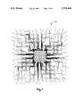
- FIG. 7illustrates a typical arrangement for signal connections from a chip pattern that is achievable in accordance with the present invention.
- a printed wiring devicesuch as a printed circuit board or card generally indicated at 10 is composed of a self-supporting planar redistribution structure 12 made in accordance with the present invention and a multi-layer substrate 14.
- Multi-layer substrate 14is a laminate composed of two signal layers 16 and one power plane or core 18 laminated together to form a coherent composite.
- Plated-through-holes 20are provided in substrate 14 for electrical connection to various electronic devices, not shown.
- the interior surfaces of plated-through-holes 20are provided with layers of metal plating 22 which extend past top surface 24 of printed wiring device 14 thereby forming metal ridges 26 surrounding each plated-through-hole.
- Inventive planar redistribution structure 12is composed of a dielectric layer or sheet 28 having an upper or first major surface 30, a lower or second major surface 32 and multiple vias or openings 42 communicating between these two surfaces.
- First major surface 30carries input/output pads 34 and redistribution lines 36.
- input/output pads 34cover each of vias 42 and are also larger in diameter than vias 42.
- redistribution lines 36are arranged in a fan-out pattern as illustrated generally at 38 in FIG. 7 for redistributing signals from and to semiconductor chip in area 40 to various electrical contacts in printed wiring device 14.
- input/output pads 34define an even topography with redistribution lines 36 at upper surface 30 of planar redistribution structure 12.
- input/output pads 34are substantially the same height as redistribution lines 36, whereby the upper surfaces of the signal redistribution lines and the input/output pads are essentially coplanar. This feature not only facilitates flip chip joining but also allows the contact pads and redistribution lines to be easily made by fine line lithography.
- vias 42take the form of plated-through-holes in that the interior walls of vias 42 are provided with metal plating layers 44 thereon. Metal plating also extends over the closed tops of vias 42 to form top plating 46 which is in secure electrical contact with input/output pads 34 carried on upper major surface 30 of the inventive planar redistribution structure 12.
- Lower or second major surface 32 of dielectric layer 28carries ground plane 48 over a substantial portion of its entire surface area.
- metalis deposited in vias 42 for forming metal plating layers 44 and tops 46, it is also allowed to deposit on ground plane 48 in the areas immediately adjacent the individual vias.
- Thisforms joining patterns 49, 50 and 51 on lower major surface 32, which joining patterns are in intimate electrical contact with metal plating layers 44 and top plating 46 of the vias.
- joining patterns 49, 50 and 51are larger in lateral dimension than input/output pads 34 on upper major surface 30 of the redistribution structure.
- joining patterns 49, 50 and 51approximately match metal ridges 26 on substrate 14 in overall lateral dimension. This facilitates good electrical contact between planar redistribution structure 12 and substrate 14 when the two are laminated together.
- portions of ground plane 48have been removed to form openings or breaks 52 therein. These breaks electrically insulate joining patterns 49 and 51 from the ground plane, joining patterns 49 and 51 thereby forming a power joining pattern for electrical connection to power plane 18 in substrate 14 and a signal joining pattern for electrical connection to one of the signal layers 16 in substrate 14, respectively.
- the structure of the inventive planar redistribution structureleads to many advantages.
- the even topology of input/output pads 34 and signal redistribution lines 36facilitates flip chip joining as well as easy fabrication by simple fine line lithography.
- the larger size of joining patterns 49, 50 and 51 relative to input/output pads 34leads to excellent power and ground connections when the inventive redistribution structure is laminated to its multi-layer substrate. This not only improves fabrication yields, but also leads to minimum capacitive loadings on the signal lines.
- ground plane 48is provided on lower major surface 32 of dielectric layer 28, redistribution lines 36 exhibit excellent Z o (characteristic impedance) control.
- an essentially continuous ground planeimparts excellent dimensional stability to the inventive planar redistribution structure.
- dielectric layer 28is made from a fluoropolymer based material, while input/output pads 34, redistribution lines 36, ground plane 48, joining patterns 49, 50 and 51 and metal plating layers 44 and 46 on vias 42 are all made from copper.
- dielectric layer 28is made no more than 100 ⁇ m thick, preferably no more than 50 ⁇ m thick.
- vias 42can be easily formed by laser ablation using a CO 2 pulsed laser.
- the pitch between the individual contact bumps of chip 40can be about 250 ⁇ m, while the center-to-center pitch of vias 42 is substantially greater, preferably at least about twice as great as the pitch between these contact bumps. It can therefore be seen that the inventive planar redistribution structure, although very thin and easy to manufacture, nonetheless can receive and securely mount a chip while at the same time distributing its signal to a printed wiring device of considerably larger dimension.
- FIG. 2 to 6illustrate one way of producing the inventive planar redistribution structure of FIG. 1.
- a fluoropolymer dielectric sheet 54 clad with continuous copper layers 56 and 58is laminated on both sides with dry film resist layers 60 and 62, respectively.
- dry film resist 60is exposed to a pattern corresponding to input/output pads 34 and redistribution lines 36, while resist 62 is exposed to a pattern corresponding to via holes 42.
- Resists 60 and 62are then developed to remove selected portions of the resist layers and then the copper layers 56 and 58 under these exposed areas are etched away with a suitable etchant to leave the structure illustrated in FIG. 2.
- lower major surface 66 of the dielectric sheetis subjected to laser ablation to form via holes 42 therein.
- resist layers 60 and 62are stripped away to leave the structure illustrated in FIG. 3.
- Via holes 42 including the surrounding areas of ground plane 48are then electrolytically plated with copper followed by gold to thereby form joining patterns 49, 50 and 51, as illustrated in FIG. 5. Then, negative dry resist layers 68 and 70 are stripped off to form the structure illustrated in FIG. 5.
- openings or breaks 52 for electrically insulating forming patterns 49 and 51are formed in ground plane 48 by applying a dry film negative resist to both sides of the structure of FIG. 5 and exposing and developing the negative dry resist on lower major surface 66 in the pattern of these openings.
- the negative dry resist layers on both surfaces for electrically insulating forming patterns 49 and 51are then stripped away and finally upper major surface 64 is flash-etched to remove the remaining thin layer of copper thereon in non-signal areas.
- the inventive planar redistribution structure produced in accordance with the present invention, as well as a printed wiring device formed from this planar redistribution structure,have many advantages. For example, because the redistribution lines and input/output pads on the upper major surface of the inventive redistribution structure are coplanar, joining of the redistribution structure to flip chips is facilitated. Also, production of these lines and pads can be done very easily in the same processing step, for example by fine line lithography. Moreover, because of ground plane 48, the redistribution signal lines have excellent Z o control. Also, ground plane 48 provides excellent dimensional stability to the inventive redistribution structure.
- inventive planar redistribution structureallows each surface to be tailor-made to match the device to which it will be attached, i.e. the semiconductor chip on one side and the multi-layer substrate on the other.
- the inventive planar redistribution structureeven though it is very thin and easy to manufacture, can nonetheless connect these two devices very easily and securely.
- a further advantage of the inventive planar redistribution structureresides in the fact that joining patterns 49, 50 and 51 can be made considerably larger in lateral dimension than input/output pads 34. This not only improves fabrication yield during parallel lamination with a printed wiring device but also provides for excellent electrical connection since the contacts at the printed wiring device are considerably bigger.
- the inventive planar redistribution structureis separately made from the printed wiring device allows off-specification redistribution structures to be discarded before lamination to on-specification multi-layer substrates. This improves fabrication yields because off-specification redistribution structures can be identified and discarded before use.
- planar redistribution structureswith improved thermal expansion properties, i.e. superior coefficients of thermal expansion (CTE's).
- CTE'scoefficients of thermal expansion
- a planar redistribution structurecan be made by the general procedure described above.
- a preferred procedure for making this redistribution structureis as follows:
- a CIC-clad fluorocarbon polymer dielectric sheetis laminated one side (side-A) with a first dry film resist (DF-1) and on its other side (side-B) with a different dry film resist (DF-2), resists DF-1 and DF-2 being developed by different strippers.
- DF-1dry film resist
- DF-2dry film resist
- patterns for the redistribution lines and input/output padsare exposed and developed on side-A, while patterns for the vias are exposed and developed on side-B.
- both external copper and invarare etched from both side-A and side-B. The layer of copper in contact with the fluoropolymer dielectric is not etched at this point.
- directional etching techniquesfor example fluid head etching tools, are used to fully etch away remaining copper from the via hole area on side-B.
- the remaining copper layeris only partially etched, away in thickness from the non-signal areas.
- a negative resistis electrodeposited to both Side-A and Side-B, this resist also being developed by a different stripper from resists DF-1 and DF-2.
- This negative resistis applied to Side-A so as to cover all non-signal areas as well as the side walls of all signal lines. It is also applied to Side-B to cover the metal sidewalls surrounding the via hole area.
- resist DF-1is stripped from the signal line patterns on side-A and then first the copper and then the invar thereunder are etched away. Then, copper is electrolytically pattern plated to the signal line patterns on side-A to a thickness comparable to the entire thickness of the CIC layer. If desired, a thin layer of barrier metal can also be applied to protect the plated copper from the etching process to be performed in the next step.
- the electrodeposited negative resistis stripped from the non-signal areas and the copper thereon etched away, preferably using directional etching techniques (side-A). If a barrier metal is not used, the plated copper in the signal area will be slightly reduced in thickness during the etching of the thin copper in the non-signal areas. Also, if a barrier metal has been applied to the top of the signal lines, as indicated above in the preferred embodiment, this barrier metal is then flash etched away.
- vias or holes 42are formed in the fluoropolymer dielectric sheet by laser ablation, using resist DF-2 and side-B CIC ground layer as the ablation mask. Then, resist DF-2 is stripped from side-B. After this step, the structure is processed in the same way as described above to plate the via holes and adjoining areas with metal to form plated-through-holes and joining patterns followed by forming breaks 52 for isolating the power joining patterns and the signal joining patterns. Of course, in forming breaks 52, copper, then invar, then copper must be etched away from the structure to form these rings.
- a completed device formed in this manneris essentially the same as the device illustrated in FIG. 1 in terms of structure, except that ground plane 48 is formed from a CIC composite. Because the thermal expansion characteristics of a CIC composite are more closely matched to that of the integrated circuit chip to be mounted to the completed structure at a later time, the planar redistribution structure formed in this manner can accommodate even greater amounts of thermal stress than the structure illustrated in FIG. 1.
- via holes 42can be formed in dielectric 28 by means other than CO 2 laser, e.g., by plasma etching using the copper layer 48 as an etching mask, or, if material 28 is photosensitive, by using copper layer 48 as a photomask.
- multi-layer substrate 14is composed of two signal layers and one power plane or core
- multi-layer substrates of other designscan also be used.
- the present inventionfinds particular applicability in manufacturing printed wiring devices from 2S3P multi-layer substrates as well. It should be appreciated that the invention is applicable for use with printed wiring devices of any structure.
Landscapes
- Engineering & Computer Science (AREA)
- Microelectronics & Electronic Packaging (AREA)
- Physics & Mathematics (AREA)
- Condensed Matter Physics & Semiconductors (AREA)
- General Physics & Mathematics (AREA)
- Computer Hardware Design (AREA)
- Power Engineering (AREA)
- Manufacturing & Machinery (AREA)
- Production Of Multi-Layered Print Wiring Board (AREA)
Abstract
Description
Claims (11)
Priority Applications (3)
| Application Number | Priority Date | Filing Date | Title |
|---|---|---|---|
| US08/697,655US5774340A (en) | 1996-08-28 | 1996-08-28 | Planar redistribution structure and printed wiring device |
| KR1019970023029AKR100271838B1 (en) | 1996-08-28 | 1997-06-04 | Planar redistribution structure and printed wiring device |
| US09/062,816US6000130A (en) | 1996-08-28 | 1998-04-20 | Process for making planar redistribution structure |
Applications Claiming Priority (1)
| Application Number | Priority Date | Filing Date | Title |
|---|---|---|---|
| US08/697,655US5774340A (en) | 1996-08-28 | 1996-08-28 | Planar redistribution structure and printed wiring device |
Related Child Applications (1)
| Application Number | Title | Priority Date | Filing Date |
|---|---|---|---|
| US09/062,816DivisionUS6000130A (en) | 1996-08-28 | 1998-04-20 | Process for making planar redistribution structure |
Publications (1)
| Publication Number | Publication Date |
|---|---|
| US5774340Atrue US5774340A (en) | 1998-06-30 |
Family
ID=24801982
Family Applications (2)
| Application Number | Title | Priority Date | Filing Date |
|---|---|---|---|
| US08/697,655Expired - LifetimeUS5774340A (en) | 1996-08-28 | 1996-08-28 | Planar redistribution structure and printed wiring device |
| US09/062,816Expired - Fee RelatedUS6000130A (en) | 1996-08-28 | 1998-04-20 | Process for making planar redistribution structure |
Family Applications After (1)
| Application Number | Title | Priority Date | Filing Date |
|---|---|---|---|
| US09/062,816Expired - Fee RelatedUS6000130A (en) | 1996-08-28 | 1998-04-20 | Process for making planar redistribution structure |
Country Status (2)
| Country | Link |
|---|---|
| US (2) | US5774340A (en) |
| KR (1) | KR100271838B1 (en) |
Cited By (150)
| Publication number | Priority date | Publication date | Assignee | Title |
|---|---|---|---|---|
| US6018196A (en)* | 1996-11-08 | 2000-01-25 | W. L. Gore & Associates, Inc. | Semiconductor flip chip package |
| US6175087B1 (en)* | 1998-12-02 | 2001-01-16 | International Business Machines Corporation | Composite laminate circuit structure and method of forming the same |
| US6191472B1 (en)* | 1999-01-05 | 2001-02-20 | Intel Corporation | Hole geometry of a semiconductor package substrate |
| US6204453B1 (en)* | 1998-12-02 | 2001-03-20 | International Business Machines Corporation | Two signal one power plane circuit board |
| US6291777B1 (en)* | 1999-02-17 | 2001-09-18 | Applied Materials, Inc. | Conductive feed-through for creating a surface electrode connection within a dielectric body and method of fabricating same |
| WO2001076331A1 (en)* | 2000-03-31 | 2001-10-11 | Dyconex Patente Ag | Element for an electronic assembly |
| US6310398B1 (en) | 1998-12-03 | 2001-10-30 | Walter M. Katz | Routable high-density interfaces for integrated circuit devices |
| US6316830B1 (en) | 1998-12-17 | 2001-11-13 | Charles Wen Chyang Lin | Bumpless flip chip assembly with strips and via-fill |
| US6350632B1 (en) | 2000-09-20 | 2002-02-26 | Charles W. C. Lin | Semiconductor chip assembly with ball bond connection joint |
| US6350633B1 (en) | 2000-08-22 | 2002-02-26 | Charles W. C. Lin | Semiconductor chip assembly with simultaneously electroplated contact terminal and connection joint |
| US6350386B1 (en) | 2000-09-20 | 2002-02-26 | Charles W. C. Lin | Method of making a support circuit with a tapered through-hole for a semiconductor chip assembly |
| US6381120B2 (en)* | 1998-08-25 | 2002-04-30 | Murata Manufacturing Co., Ltd. | Mounting arrangement for multilayer electronic part |
| US6403400B2 (en) | 1998-12-17 | 2002-06-11 | Charles Wen Chyang Lin | Bumpless flip chip assembly with strips-in-via and plating |
| US6402970B1 (en) | 2000-08-22 | 2002-06-11 | Charles W. C. Lin | Method of making a support circuit for a semiconductor chip assembly |
| US6403460B1 (en) | 2000-08-22 | 2002-06-11 | Charles W. C. Lin | Method of making a semiconductor chip assembly |
| US6406939B1 (en) | 1998-05-02 | 2002-06-18 | Charles W. C. Lin | Flip chip assembly with via interconnection |
| US6436734B1 (en) | 2000-08-22 | 2002-08-20 | Charles W. C. Lin | Method of making a support circuit for a semiconductor chip assembly |
| US6440835B1 (en) | 2000-10-13 | 2002-08-27 | Charles W. C. Lin | Method of connecting a conductive trace to a semiconductor chip |
| US6444489B1 (en) | 2000-12-15 | 2002-09-03 | Charles W. C. Lin | Semiconductor chip assembly with bumped molded substrate |
| US6448108B1 (en) | 2000-10-02 | 2002-09-10 | Charles W. C. Lin | Method of making a semiconductor chip assembly with a conductive trace subtractively formed before and after chip attachment |
| US6448644B1 (en) | 1998-05-02 | 2002-09-10 | Charles W. C. Lin | Flip chip assembly with via interconnection |
| US6479765B2 (en)* | 2000-06-26 | 2002-11-12 | Robinson Nugent, Inc. | Vialess printed circuit board |
| US6492252B1 (en) | 2000-10-13 | 2002-12-10 | Bridge Semiconductor Corporation | Method of connecting a bumped conductive trace to a semiconductor chip |
| US6495770B2 (en)* | 2000-12-04 | 2002-12-17 | Intel Corporation | Electronic assembly providing shunting of electrical current |
| US6511901B1 (en) | 1999-11-05 | 2003-01-28 | Atmel Corporation | Metal redistribution layer having solderable pads and wire bondable pads |
| US6511865B1 (en) | 2000-09-20 | 2003-01-28 | Charles W. C. Lin | Method for forming a ball bond connection joint on a conductive trace and conductive pad in a semiconductor chip assembly |
| US6518509B1 (en)* | 1999-12-23 | 2003-02-11 | International Business Machines Corporation | Copper plated invar with acid preclean |
| US6521843B1 (en)* | 1998-05-13 | 2003-02-18 | Nec Corporation | Multilayer printed circuit board having signal, power and ground through holes |
| US6528891B2 (en) | 1998-12-17 | 2003-03-04 | Charles Wen Chyang Lin | Bumpless flip chip assembly with solder via |
| US6537851B1 (en) | 2000-10-13 | 2003-03-25 | Bridge Semiconductor Corporation | Method of connecting a bumped compliant conductive trace to a semiconductor chip |
| US6544813B1 (en) | 2000-10-02 | 2003-04-08 | Charles W. C. Lin | Method of making a semiconductor chip assembly with a conductive trace subtractively formed before and after chip attachment |
| US6548393B1 (en) | 2000-10-13 | 2003-04-15 | Charles W. C. Lin | Semiconductor chip assembly with hardened connection joint |
| US6551861B1 (en) | 2000-08-22 | 2003-04-22 | Charles W. C. Lin | Method of making a semiconductor chip assembly by joining the chip to a support circuit with an adhesive |
| US6562709B1 (en) | 2000-08-22 | 2003-05-13 | Charles W. C. Lin | Semiconductor chip assembly with simultaneously electroplated contact terminal and connection joint |
| US6562657B1 (en) | 2000-08-22 | 2003-05-13 | Charles W. C. Lin | Semiconductor chip assembly with simultaneously electrolessly plated contact terminal and connection joint |
| US6576493B1 (en) | 2000-10-13 | 2003-06-10 | Bridge Semiconductor Corporation | Method of connecting a conductive trace and an insulative base to a semiconductor chip using multiple etch steps |
| US6576539B1 (en) | 2000-10-13 | 2003-06-10 | Charles W.C. Lin | Semiconductor chip assembly with interlocked conductive trace |
| US6583040B1 (en) | 2000-10-13 | 2003-06-24 | Bridge Semiconductor Corporation | Method of making a pillar in a laminated structure for a semiconductor chip assembly |
| US20030136578A1 (en)* | 2000-08-10 | 2003-07-24 | Sony Chemicals Corp. | Flexible wiring boards for double-side connection |
| US6617527B2 (en)* | 2000-10-03 | 2003-09-09 | Victor Company Of Japan, Limited | Printed circuit board having a pair of grooves extending the entire length |
| US6653170B1 (en) | 2001-02-06 | 2003-11-25 | Charles W. C. Lin | Semiconductor chip assembly with elongated wire ball bonded to chip and electrolessly plated to support circuit |
| US20030222282A1 (en)* | 2002-04-29 | 2003-12-04 | Fjelstad Joseph C. | Direct-connect signaling system |
| US6660945B2 (en) | 2001-10-16 | 2003-12-09 | International Business Machines Corporation | Interconnect structure and method of making same |
| US6660626B1 (en) | 2000-08-22 | 2003-12-09 | Charles W. C. Lin | Semiconductor chip assembly with simultaneously electrolessly plated contact terminal and connection joint |
| US6667229B1 (en) | 2000-10-13 | 2003-12-23 | Bridge Semiconductor Corporation | Method of connecting a bumped compliant conductive trace and an insulative base to a semiconductor chip |
| US6699780B1 (en) | 2000-10-13 | 2004-03-02 | Bridge Semiconductor Corporation | Method of connecting a conductive trace to a semiconductor chip using plasma undercut etching |
| US6740576B1 (en) | 2000-10-13 | 2004-05-25 | Bridge Semiconductor Corporation | Method of making a contact terminal with a plated metal peripheral sidewall portion for a semiconductor chip assembly |
| US6750405B1 (en)* | 1995-06-07 | 2004-06-15 | International Business Machines Corporation | Two signal one power plane circuit board |
| US20040155337A1 (en)* | 2003-02-06 | 2004-08-12 | Kulicke & Soffa Investments, Inc. | High density chip level package for the packaging of integrated circuits and method to manufacture same |
| US6803528B1 (en)* | 1999-11-05 | 2004-10-12 | 3M Innovative Properties Company | Multi-layer double-sided wiring board and method of fabricating the same |
| US6831371B1 (en) | 2002-03-16 | 2004-12-14 | Amkor Technology, Inc. | Integrated circuit substrate having embedded wire conductors and method therefor |
| US20050014395A1 (en)* | 2003-01-13 | 2005-01-20 | Fjelstad Joseph C. | System for making high-speed connections to board-mounted modules |
| US20050041398A1 (en)* | 2002-05-01 | 2005-02-24 | Huemoeller Ronald Patrick | Integrated circuit substrate having embedded back-side access conductors and vias |
| US6872591B1 (en) | 2000-10-13 | 2005-03-29 | Bridge Semiconductor Corporation | Method of making a semiconductor chip assembly with a conductive trace and a substrate |
| US6876072B1 (en) | 2000-10-13 | 2005-04-05 | Bridge Semiconductor Corporation | Semiconductor chip assembly with chip in substrate cavity |
| US6891272B1 (en) | 2002-07-31 | 2005-05-10 | Silicon Pipe, Inc. | Multi-path via interconnection structures and methods for manufacturing the same |
| US6908788B1 (en) | 2000-10-13 | 2005-06-21 | Bridge Semiconductor Corporation | Method of connecting a conductive trace to a semiconductor chip using a metal base |
| US6930257B1 (en) | 2002-05-01 | 2005-08-16 | Amkor Technology, Inc. | Integrated circuit substrate having laminated laser-embedded circuit layers |
| US6930256B1 (en) | 2002-05-01 | 2005-08-16 | Amkor Technology, Inc. | Integrated circuit substrate having laser-embedded conductive patterns and method therefor |
| US6949408B1 (en) | 2000-10-13 | 2005-09-27 | Bridge Semiconductor Corporation | Method of connecting a conductive trace and an insulative base to a semiconductor chip using multiple etch steps |
| US6984576B1 (en) | 2000-10-13 | 2006-01-10 | Bridge Semiconductor Corporation | Method of connecting an additively and subtractively formed conductive trace and an insulative base to a semiconductor chip |
| US6987661B1 (en) | 2001-06-19 | 2006-01-17 | Amkor Technology, Inc. | Integrated circuit substrate having embedded passive components and methods therefor |
| US20060012024A1 (en)* | 2000-10-13 | 2006-01-19 | Bridge Semiconductor Corporation | Semiconductor chip assembly with metal containment wall and solder terminal |
| US7009297B1 (en) | 2000-10-13 | 2006-03-07 | Bridge Semiconductor Corporation | Semiconductor chip assembly with embedded metal particle |
| US7028400B1 (en) | 2002-05-01 | 2006-04-18 | Amkor Technology, Inc. | Integrated circuit substrate having laser-exposed terminals |
| US7071089B1 (en) | 2000-10-13 | 2006-07-04 | Bridge Semiconductor Corporation | Method of making a semiconductor chip assembly with a carved bumped terminal |
| US7075186B1 (en) | 2000-10-13 | 2006-07-11 | Bridge Semiconductor Corporation | Semiconductor chip assembly with interlocked contact terminal |
| US7094676B1 (en) | 2000-10-13 | 2006-08-22 | Bridge Semiconductor Corporation | Semiconductor chip assembly with embedded metal pillar |
| US7112521B1 (en) | 2000-10-13 | 2006-09-26 | Bridge Semiconductor Corporation | Method of making a semiconductor chip assembly with a bumped metal pillar |
| US20060220215A1 (en)* | 2005-03-18 | 2006-10-05 | Jong-Joo Lee | Semiconductor chips having redistributed power/ground lines directly connected to power/ground lines of internal circuits and methods of fabricating the same |
| US7129113B1 (en) | 2000-10-13 | 2006-10-31 | Bridge Semiconductor Corporation | Method of making a three-dimensional stacked semiconductor package with a metal pillar in an encapsulant aperture |
| US7132741B1 (en) | 2000-10-13 | 2006-11-07 | Bridge Semiconductor Corporation | Semiconductor chip assembly with carved bumped terminal |
| US20060258139A1 (en)* | 1999-10-12 | 2006-11-16 | Tessera Interconnect Materials, Inc. | Manufacturing method for wiring circuit substrate |
| US20060267612A1 (en)* | 2005-05-30 | 2006-11-30 | Ryoji Hamazaki | Automatic design method for semiconductor device |
| US7145238B1 (en) | 2004-05-05 | 2006-12-05 | Amkor Technology, Inc. | Semiconductor package and substrate having multi-level vias |
| US20070029106A1 (en)* | 2003-04-07 | 2007-02-08 | Ibiden Co., Ltd. | Multilayer printed wiring board |
| US7190080B1 (en) | 2000-10-13 | 2007-03-13 | Bridge Semiconductor Corporation | Semiconductor chip assembly with embedded metal pillar |
| US20070126443A1 (en)* | 2001-07-11 | 2007-06-07 | Formfactor, Inc. | Method of Manufacturing A Probe Card |
| US20070163887A1 (en)* | 2004-01-29 | 2007-07-19 | Hofmann Hannes P | Method of manufacturing a circuit carrier and the use of the method |
| US7262082B1 (en) | 2000-10-13 | 2007-08-28 | Bridge Semiconductor Corporation | Method of making a three-dimensional stacked semiconductor package with a metal pillar and a conductive interconnect in an encapsulant aperture |
| US7264991B1 (en) | 2000-10-13 | 2007-09-04 | Bridge Semiconductor Corporation | Method of connecting a conductive trace to a semiconductor chip using conductive adhesive |
| US7268421B1 (en) | 2004-11-10 | 2007-09-11 | Bridge Semiconductor Corporation | Semiconductor chip assembly with welded metal pillar that includes enlarged ball bond |
| US20080001286A1 (en)* | 2006-06-29 | 2008-01-03 | Bram Leader | Shielded via |
| US7319265B1 (en) | 2000-10-13 | 2008-01-15 | Bridge Semiconductor Corporation | Semiconductor chip assembly with precision-formed metal pillar |
| US20080043447A1 (en)* | 2002-05-01 | 2008-02-21 | Amkor Technology, Inc. | Semiconductor package having laser-embedded terminals |
| US7334326B1 (en) | 2001-06-19 | 2008-02-26 | Amkor Technology, Inc. | Method for making an integrated circuit substrate having embedded passive components |
| US20080048688A1 (en)* | 2000-03-17 | 2008-02-28 | Formfactor, Inc. | Methods for planarizing a semiconductor contactor |
| US7396703B1 (en) | 2003-11-20 | 2008-07-08 | Bridge Semiconductor Corporation | Method of making a semiconductor chip assembly with a bumped terminal and a filler |
| US7446419B1 (en) | 2004-11-10 | 2008-11-04 | Bridge Semiconductor Corporation | Semiconductor chip assembly with welded metal pillar of stacked metal balls |
| US7494843B1 (en) | 2006-12-26 | 2009-02-24 | Bridge Semiconductor Corporation | Method of making a semiconductor chip assembly with thermal conductor and encapsulant grinding |
| US7504711B2 (en) | 2004-07-21 | 2009-03-17 | Infineon Technologies Ag | Semiconductor substrate with strip conductors formed of carbon nanotubes and production thereof |
| US20090090542A1 (en)* | 2004-02-04 | 2009-04-09 | Ibiden Co., Ltd. | Multilayer printed wiring board |
| US7538415B1 (en) | 2003-11-20 | 2009-05-26 | Bridge Semiconductor Corporation | Semiconductor chip assembly with bumped terminal, filler and insulative base |
| US7548430B1 (en) | 2002-05-01 | 2009-06-16 | Amkor Technology, Inc. | Buildup dielectric and metallization process and semiconductor package |
| US7550857B1 (en) | 2006-11-16 | 2009-06-23 | Amkor Technology, Inc. | Stacked redistribution layer (RDL) die assembly package |
| US7589398B1 (en) | 2006-10-04 | 2009-09-15 | Amkor Technology, Inc. | Embedded metal features structure |
| US20090291573A1 (en)* | 1993-11-16 | 2009-11-26 | Formfactor, Inc. | Probe card assembly and kit, and methods of making same |
| US7633765B1 (en) | 2004-03-23 | 2009-12-15 | Amkor Technology, Inc. | Semiconductor package including a top-surface metal layer for implementing circuit features |
| US7670962B2 (en) | 2002-05-01 | 2010-03-02 | Amkor Technology, Inc. | Substrate having stiffener fabrication method |
| DE102009023629A1 (en)* | 2008-11-14 | 2010-05-20 | Samsung Electro - Mechanics Co., Ltd., Suwon | Printed circuit board and manufacturing process |
| US7750250B1 (en) | 2006-12-22 | 2010-07-06 | Amkor Technology, Inc. | Blind via capture pad structure |
| US7750446B2 (en) | 2002-04-29 | 2010-07-06 | Interconnect Portfolio Llc | IC package structures having separate circuit interconnection structures and assemblies constructed thereof |
| US7750483B1 (en) | 2004-11-10 | 2010-07-06 | Bridge Semiconductor Corporation | Semiconductor chip assembly with welded metal pillar and enlarged plated contact terminal |
| US7752752B1 (en) | 2007-01-09 | 2010-07-13 | Amkor Technology, Inc. | Method of fabricating an embedded circuit pattern |
| US7811863B1 (en) | 2006-10-26 | 2010-10-12 | Bridge Semiconductor Corporation | Method of making a semiconductor chip assembly with metal pillar and encapsulant grinding and heat sink attachment |
| CN101330130B (en)* | 2007-06-18 | 2011-02-02 | 惠好公司 | Fabrication of self-aligned via holes in polymer thin films |
| US7960827B1 (en) | 2009-04-09 | 2011-06-14 | Amkor Technology, Inc. | Thermal via heat spreader package and method |
| US7993983B1 (en) | 2003-11-17 | 2011-08-09 | Bridge Semiconductor Corporation | Method of making a semiconductor chip assembly with chip and encapsulant grinding |
| US8222538B1 (en) | 2009-06-12 | 2012-07-17 | Amkor Technology, Inc. | Stackable via package and method |
| US8294276B1 (en) | 2010-05-27 | 2012-10-23 | Amkor Technology, Inc. | Semiconductor device and fabricating method thereof |
| US8300423B1 (en) | 2010-05-25 | 2012-10-30 | Amkor Technology, Inc. | Stackable treated via package and method |
| US8323771B1 (en) | 2007-08-15 | 2012-12-04 | Amkor Technology, Inc. | Straight conductor blind via capture pad structure and fabrication method |
| US8337657B1 (en) | 2010-10-27 | 2012-12-25 | Amkor Technology, Inc. | Mechanical tape separation package and method |
| US8338229B1 (en) | 2010-07-30 | 2012-12-25 | Amkor Technology, Inc. | Stackable plasma cleaned via package and method |
| US8471154B1 (en) | 2009-08-06 | 2013-06-25 | Amkor Technology, Inc. | Stackable variable height via package and method |
| US8482134B1 (en) | 2010-11-01 | 2013-07-09 | Amkor Technology, Inc. | Stackable package and method |
| US8485418B2 (en) | 1995-05-26 | 2013-07-16 | Formfactor, Inc. | Method of wirebonding that utilizes a gas flow within a capillary from which a wire is played out |
| US8525318B1 (en) | 2010-11-10 | 2013-09-03 | Amkor Technology, Inc. | Semiconductor device and fabricating method thereof |
| US8535961B1 (en) | 2010-12-09 | 2013-09-17 | Amkor Technology, Inc. | Light emitting diode (LED) package and method |
| US8536462B1 (en) | 2010-01-22 | 2013-09-17 | Amkor Technology, Inc. | Flex circuit package and method |
| US8557629B1 (en) | 2010-12-03 | 2013-10-15 | Amkor Technology, Inc. | Semiconductor device having overlapped via apertures |
| US8623753B1 (en) | 2009-05-28 | 2014-01-07 | Amkor Technology, Inc. | Stackable protruding via package and method |
| US8633598B1 (en) | 2011-09-20 | 2014-01-21 | Amkor Technology, Inc. | Underfill contacting stacking balls package fabrication method and structure |
| US8653674B1 (en) | 2011-09-15 | 2014-02-18 | Amkor Technology, Inc. | Electronic component package fabrication method and structure |
| US8717775B1 (en) | 2010-08-02 | 2014-05-06 | Amkor Technology, Inc. | Fingerprint sensor package and method |
| US8796561B1 (en) | 2009-10-05 | 2014-08-05 | Amkor Technology, Inc. | Fan out build up substrate stackable package and method |
| US8826531B1 (en) | 2005-04-05 | 2014-09-09 | Amkor Technology, Inc. | Method for making an integrated circuit substrate having laminated laser-embedded circuit layers |
| US20140305688A1 (en)* | 2013-04-15 | 2014-10-16 | Canon Kabushiki Kaisha | Printed wiring board and printed circuit board |
| US8872329B1 (en) | 2009-01-09 | 2014-10-28 | Amkor Technology, Inc. | Extended landing pad substrate package structure and method |
| US8890329B2 (en) | 2011-04-26 | 2014-11-18 | Amkor Technology, Inc. | Semiconductor device |
| US8937381B1 (en) | 2009-12-03 | 2015-01-20 | Amkor Technology, Inc. | Thin stackable package and method |
| US9013011B1 (en) | 2011-03-11 | 2015-04-21 | Amkor Technology, Inc. | Stacked and staggered die MEMS package and method |
| US9029962B1 (en) | 2011-10-12 | 2015-05-12 | Amkor Technology, Inc. | Molded cavity substrate MEMS package fabrication method and structure |
| US20150201497A1 (en)* | 2009-12-16 | 2015-07-16 | Intel Corporation | High-density inter-package connections for ultra-thin package-on-package structures, and processes of forming same |
| US9365947B2 (en) | 2013-10-04 | 2016-06-14 | Invensas Corporation | Method for preparing low cost substrates |
| US9391043B2 (en) | 2012-11-20 | 2016-07-12 | Amkor Technology, Inc. | Semiconductor device and manufacturing method thereof |
| US9543242B1 (en) | 2013-01-29 | 2017-01-10 | Amkor Technology, Inc. | Semiconductor package and fabricating method thereof |
| US9691734B1 (en) | 2009-12-07 | 2017-06-27 | Amkor Technology, Inc. | Method of forming a plurality of electronic component packages |
| US9691635B1 (en) | 2002-05-01 | 2017-06-27 | Amkor Technology, Inc. | Buildup dielectric layer having metallization pattern semiconductor package fabrication method |
| US9704842B2 (en) | 2013-11-04 | 2017-07-11 | Amkor Technology, Inc. | Interposer, manufacturing method thereof, semiconductor package using the same, and method for fabricating the semiconductor package |
| US9704747B2 (en) | 2013-03-29 | 2017-07-11 | Amkor Technology, Inc. | Semiconductor device and manufacturing method thereof |
| US9721872B1 (en) | 2011-02-18 | 2017-08-01 | Amkor Technology, Inc. | Methods and structures for increasing the allowable die size in TMV packages |
| US9748154B1 (en) | 2010-11-04 | 2017-08-29 | Amkor Technology, Inc. | Wafer level fan out semiconductor device and manufacturing method thereof |
| US9960328B2 (en) | 2016-09-06 | 2018-05-01 | Amkor Technology, Inc. | Semiconductor device and manufacturing method thereof |
| US10211141B1 (en)* | 2017-11-17 | 2019-02-19 | General Electric Company | Semiconductor logic device and system and method of embedded packaging of same |
| US10276523B1 (en)* | 2017-11-17 | 2019-04-30 | General Electric Company | Semiconductor logic device and system and method of embedded packaging of same |
| US10396053B2 (en) | 2017-11-17 | 2019-08-27 | General Electric Company | Semiconductor logic device and system and method of embedded packaging of same |
| US10566301B2 (en) | 2017-11-17 | 2020-02-18 | General Electric Company | Semiconductor logic device and system and method of embedded packaging of same |
| US10811277B2 (en) | 2004-03-23 | 2020-10-20 | Amkor Technology, Inc. | Encapsulated semiconductor package |
| US11081370B2 (en) | 2004-03-23 | 2021-08-03 | Amkor Technology Singapore Holding Pte. Ltd. | Methods of manufacturing an encapsulated semiconductor device |
Families Citing this family (17)
| Publication number | Priority date | Publication date | Assignee | Title |
|---|---|---|---|---|
| US6720502B1 (en)* | 2000-05-15 | 2004-04-13 | International Business Machine Corporation | Integrated circuit structure |
| JP2002026515A (en)* | 2000-07-07 | 2002-01-25 | Toshiba Corp | Printed wiring board and method of manufacturing the same |
| US6551856B1 (en)* | 2000-08-11 | 2003-04-22 | Taiwan Semiconductor Manufacturing Co., Ltd. | Method for forming copper pad redistribution and device formed |
| US20030178388A1 (en)* | 2002-03-22 | 2003-09-25 | Phillips Kenneth L. | Inverted micro-vias |
| USD512296S1 (en) | 2004-07-29 | 2005-12-06 | Great Neck Saw Manufacturers, Inc. | Utility knife |
| US7851709B2 (en)* | 2006-03-22 | 2010-12-14 | Advanced Semiconductor Engineering, Inc. | Multi-layer circuit board having ground shielding walls |
| US8097946B2 (en)* | 2007-10-31 | 2012-01-17 | Sanyo Electric Co., Ltd. | Device mounting board, semiconductor module, and mobile device |
| KR100924559B1 (en)* | 2008-03-07 | 2009-11-02 | 주식회사 하이닉스반도체 | Manufacturing method of semiconductor package |
| KR100990940B1 (en)* | 2008-04-28 | 2010-11-01 | 주식회사 하이닉스반도체 | Boards for Manufacturing Stack Packages |
| TWI392405B (en)* | 2009-10-26 | 2013-04-01 | Unimicron Technology Corp | Circuit structure |
| TWI392419B (en)* | 2009-10-29 | 2013-04-01 | Unimicron Technology Corp | Manufacturing method of circuit structure |
| KR101097628B1 (en)* | 2010-06-21 | 2011-12-22 | 삼성전기주식회사 | Printed circuit board and manufacturing method thereof |
| US20170013715A1 (en)* | 2015-07-10 | 2017-01-12 | Rohde & Schwarz Gmbh & Co. Kg | Printed circuit board and corresponding method for producing a printed circuit board |
| KR20180095350A (en)* | 2017-02-17 | 2018-08-27 | 삼성전기주식회사 | Substrate and method for manufacturing the same |
| CN109429427B (en)* | 2017-08-24 | 2020-12-15 | 鹏鼎控股(深圳)股份有限公司 | Circuit board and manufacturing method thereof |
| TWI669034B (en)* | 2018-05-11 | 2019-08-11 | 南亞電路板股份有限公司 | Printed circuit board structure and method of forming the same |
| US12015003B2 (en) | 2021-09-29 | 2024-06-18 | International Business Machines Corporation | High density interconnection and wiring layers, package structures, and integration methods |
Citations (17)
| Publication number | Priority date | Publication date | Assignee | Title |
|---|---|---|---|---|
| US4489364A (en)* | 1981-12-31 | 1984-12-18 | International Business Machines Corporation | Chip carrier with embedded engineering change lines with severable periodically spaced bridging connectors on the chip supporting surface |
| US4895752A (en)* | 1987-12-18 | 1990-01-23 | E. I. Du Pont De Nemours And Company | Low dielectric constant laminate of fluoropolymer and polyaramid |
| US4912603A (en)* | 1985-12-09 | 1990-03-27 | Fujitsu Limited | High density printed wiring board |
| US5012047A (en)* | 1987-04-06 | 1991-04-30 | Nec Corporation | Multilayer wiring substrate |
| US5097593A (en)* | 1988-12-16 | 1992-03-24 | International Business Machines Corporation | Method of forming a hybrid printed circuit board |
| US5132648A (en)* | 1990-06-08 | 1992-07-21 | Rockwell International Corporation | Large array MMIC feedthrough |
| US5194713A (en)* | 1991-10-17 | 1993-03-16 | International Business Machines Corporation | Removal of excimer laser debris using carbon dioxide laser |
| US5232548A (en)* | 1991-10-29 | 1993-08-03 | International Business Machines Corporation | Discrete fabrication of multi-layer thin film, wiring structures |
| US5243140A (en)* | 1991-10-04 | 1993-09-07 | International Business Machines Corporation | Direct distribution repair and engineering change system |
| US5294754A (en)* | 1992-12-24 | 1994-03-15 | Iternational Business Machines Corporation | Direct write EC single metal layer |
| US5358775A (en)* | 1993-07-29 | 1994-10-25 | Rogers Corporation | Fluoropolymeric electrical substrate material exhibiting low thermal coefficient of dielectric constant |
| US5367435A (en)* | 1993-11-16 | 1994-11-22 | International Business Machines Corporation | Electronic package structure and method of making same |
| US5401909A (en)* | 1992-12-12 | 1995-03-28 | International Business Machines Corporation | Printed circuit board with locally enhanced wiring density |
| US5418689A (en)* | 1993-02-01 | 1995-05-23 | International Business Machines Corporation | Printed circuit board or card for direct chip attachment and fabrication thereof |
| US5424492A (en)* | 1994-01-06 | 1995-06-13 | Dell Usa, L.P. | Optimal PCB routing methodology for high I/O density interconnect devices |
| US5578525A (en)* | 1993-12-13 | 1996-11-26 | Fujitsu Limited | Semiconductor device and a fabrication process thereof |
| US5615089A (en)* | 1994-07-26 | 1997-03-25 | Fujitsu Limited | BGA semiconductor device including a plurality of semiconductor chips located on upper and lower surfaces of a first substrate |
Family Cites Families (9)
| Publication number | Priority date | Publication date | Assignee | Title |
|---|---|---|---|---|
| US5061548A (en)* | 1987-02-17 | 1991-10-29 | Rogers Corporation | Ceramic filled fluoropolymeric composite material |
| US5384181B1 (en)* | 1987-02-17 | 2000-06-13 | World Properties Inc | Low volume fraction ceramic filled fluoropolymeric composite material |
| US5149590A (en)* | 1987-02-17 | 1992-09-22 | Rogers Corporation | Electrical substrate material |
| US4849284A (en)* | 1987-02-17 | 1989-07-18 | Rogers Corporation | Electrical substrate material |
| US4868350A (en)* | 1988-03-07 | 1989-09-19 | International Business Machines Corporation | High performance circuit boards |
| US4854038A (en)* | 1988-03-16 | 1989-08-08 | International Business Machines Corporation | Modularized fabrication of high performance printed circuit boards |
| US5010641A (en)* | 1989-06-30 | 1991-04-30 | Unisys Corp. | Method of making multilayer printed circuit board |
| US5363280A (en)* | 1993-04-22 | 1994-11-08 | International Business Machines Corporation | Printed circuit board or card thermal mass design |
| US5736679A (en)* | 1995-12-26 | 1998-04-07 | International Business Machines Corporation | Deformable interconnect structure for connecting an internal plane to a through-hole in a multilayer circuit board |
- 1996
- 1996-08-28USUS08/697,655patent/US5774340A/ennot_activeExpired - Lifetime
- 1997
- 1997-06-04KRKR1019970023029Apatent/KR100271838B1/ennot_activeExpired - Fee Related
- 1998
- 1998-04-20USUS09/062,816patent/US6000130A/ennot_activeExpired - Fee Related
Patent Citations (17)
| Publication number | Priority date | Publication date | Assignee | Title |
|---|---|---|---|---|
| US4489364A (en)* | 1981-12-31 | 1984-12-18 | International Business Machines Corporation | Chip carrier with embedded engineering change lines with severable periodically spaced bridging connectors on the chip supporting surface |
| US4912603A (en)* | 1985-12-09 | 1990-03-27 | Fujitsu Limited | High density printed wiring board |
| US5012047A (en)* | 1987-04-06 | 1991-04-30 | Nec Corporation | Multilayer wiring substrate |
| US4895752A (en)* | 1987-12-18 | 1990-01-23 | E. I. Du Pont De Nemours And Company | Low dielectric constant laminate of fluoropolymer and polyaramid |
| US5097593A (en)* | 1988-12-16 | 1992-03-24 | International Business Machines Corporation | Method of forming a hybrid printed circuit board |
| US5132648A (en)* | 1990-06-08 | 1992-07-21 | Rockwell International Corporation | Large array MMIC feedthrough |
| US5243140A (en)* | 1991-10-04 | 1993-09-07 | International Business Machines Corporation | Direct distribution repair and engineering change system |
| US5194713A (en)* | 1991-10-17 | 1993-03-16 | International Business Machines Corporation | Removal of excimer laser debris using carbon dioxide laser |
| US5232548A (en)* | 1991-10-29 | 1993-08-03 | International Business Machines Corporation | Discrete fabrication of multi-layer thin film, wiring structures |
| US5401909A (en)* | 1992-12-12 | 1995-03-28 | International Business Machines Corporation | Printed circuit board with locally enhanced wiring density |
| US5294754A (en)* | 1992-12-24 | 1994-03-15 | Iternational Business Machines Corporation | Direct write EC single metal layer |
| US5418689A (en)* | 1993-02-01 | 1995-05-23 | International Business Machines Corporation | Printed circuit board or card for direct chip attachment and fabrication thereof |
| US5358775A (en)* | 1993-07-29 | 1994-10-25 | Rogers Corporation | Fluoropolymeric electrical substrate material exhibiting low thermal coefficient of dielectric constant |
| US5367435A (en)* | 1993-11-16 | 1994-11-22 | International Business Machines Corporation | Electronic package structure and method of making same |
| US5578525A (en)* | 1993-12-13 | 1996-11-26 | Fujitsu Limited | Semiconductor device and a fabrication process thereof |
| US5424492A (en)* | 1994-01-06 | 1995-06-13 | Dell Usa, L.P. | Optimal PCB routing methodology for high I/O density interconnect devices |
| US5615089A (en)* | 1994-07-26 | 1997-03-25 | Fujitsu Limited | BGA semiconductor device including a plurality of semiconductor chips located on upper and lower surfaces of a first substrate |
Non-Patent Citations (1)
| Title |
|---|
| Microstructured Solder Mask by Means of Laser Ablation, IBM Technical Disclosure Bulletin, vol. 36, No. 11 Nov. 1993, H. Arnold, P. Lueck and W. Zapka* |
Cited By (271)
| Publication number | Priority date | Publication date | Assignee | Title |
|---|---|---|---|---|
| US20090291573A1 (en)* | 1993-11-16 | 2009-11-26 | Formfactor, Inc. | Probe card assembly and kit, and methods of making same |
| US8373428B2 (en) | 1993-11-16 | 2013-02-12 | Formfactor, Inc. | Probe card assembly and kit, and methods of making same |
| US8485418B2 (en) | 1995-05-26 | 2013-07-16 | Formfactor, Inc. | Method of wirebonding that utilizes a gas flow within a capillary from which a wire is played out |
| US6750405B1 (en)* | 1995-06-07 | 2004-06-15 | International Business Machines Corporation | Two signal one power plane circuit board |
| US6018196A (en)* | 1996-11-08 | 2000-01-25 | W. L. Gore & Associates, Inc. | Semiconductor flip chip package |
| US6448644B1 (en) | 1998-05-02 | 2002-09-10 | Charles W. C. Lin | Flip chip assembly with via interconnection |
| US6406939B1 (en) | 1998-05-02 | 2002-06-18 | Charles W. C. Lin | Flip chip assembly with via interconnection |
| US6521843B1 (en)* | 1998-05-13 | 2003-02-18 | Nec Corporation | Multilayer printed circuit board having signal, power and ground through holes |
| US6381120B2 (en)* | 1998-08-25 | 2002-04-30 | Murata Manufacturing Co., Ltd. | Mounting arrangement for multilayer electronic part |
| US6175087B1 (en)* | 1998-12-02 | 2001-01-16 | International Business Machines Corporation | Composite laminate circuit structure and method of forming the same |
| US6204453B1 (en)* | 1998-12-02 | 2001-03-20 | International Business Machines Corporation | Two signal one power plane circuit board |
| US6594811B2 (en) | 1998-12-03 | 2003-07-15 | Walter M. Katz | Routable high-density interfaces for integrated circuit devices |
| US6310398B1 (en) | 1998-12-03 | 2001-10-30 | Walter M. Katz | Routable high-density interfaces for integrated circuit devices |
| US6403400B2 (en) | 1998-12-17 | 2002-06-11 | Charles Wen Chyang Lin | Bumpless flip chip assembly with strips-in-via and plating |
| US6316830B1 (en) | 1998-12-17 | 2001-11-13 | Charles Wen Chyang Lin | Bumpless flip chip assembly with strips and via-fill |
| US6437452B2 (en) | 1998-12-17 | 2002-08-20 | Charles Wen Chyang Lin | Bumpless flip chip assembly with strips-in-via and plating |
| US6475833B2 (en) | 1998-12-17 | 2002-11-05 | Charles Wen Chyang Lin | Bumpless flip chip assembly with strips and via-fill |
| US6528891B2 (en) | 1998-12-17 | 2003-03-04 | Charles Wen Chyang Lin | Bumpless flip chip assembly with solder via |
| US6191472B1 (en)* | 1999-01-05 | 2001-02-20 | Intel Corporation | Hole geometry of a semiconductor package substrate |
| US6291777B1 (en)* | 1999-02-17 | 2001-09-18 | Applied Materials, Inc. | Conductive feed-through for creating a surface electrode connection within a dielectric body and method of fabricating same |
| US20060258139A1 (en)* | 1999-10-12 | 2006-11-16 | Tessera Interconnect Materials, Inc. | Manufacturing method for wiring circuit substrate |
| US7546681B2 (en)* | 1999-10-12 | 2009-06-16 | Tessera Interconnect Materials, Inc. | Manufacturing method for wiring circuit substrate |
| US20070209199A1 (en)* | 1999-10-12 | 2007-09-13 | Tomoo Iijima | Methods of making microelectronic assemblies |
| US7721422B2 (en) | 1999-10-12 | 2010-05-25 | Tessera Interconnect Materials, Inc. | Methods of making microelectronic assemblies |
| US6762117B2 (en)* | 1999-11-05 | 2004-07-13 | Atmel Corporation | Method of fabricating metal redistribution layer having solderable pads and wire bondable pads |
| US6577008B2 (en) | 1999-11-05 | 2003-06-10 | Atmel Corporation | Metal redistribution layer having solderable pads and wire bondable pads |
| US6803528B1 (en)* | 1999-11-05 | 2004-10-12 | 3M Innovative Properties Company | Multi-layer double-sided wiring board and method of fabricating the same |
| US6511901B1 (en) | 1999-11-05 | 2003-01-28 | Atmel Corporation | Metal redistribution layer having solderable pads and wire bondable pads |
| US20030119297A1 (en)* | 1999-11-05 | 2003-06-26 | Lam Ken M. | Metal redistribution layer having solderable pads and wire bondable pads |
| US6518509B1 (en)* | 1999-12-23 | 2003-02-11 | International Business Machines Corporation | Copper plated invar with acid preclean |
| US20110193583A1 (en)* | 2000-03-17 | 2011-08-11 | Formfactor, Inc. | Methods for planarizing a semiconductor contactor |
| US8427183B2 (en) | 2000-03-17 | 2013-04-23 | Formfactor, Inc. | Probe card assembly having an actuator for bending the probe substrate |
| US20080048688A1 (en)* | 2000-03-17 | 2008-02-28 | Formfactor, Inc. | Methods for planarizing a semiconductor contactor |
| US20100263432A1 (en)* | 2000-03-17 | 2010-10-21 | Formfactor, Inc. | Methods for planarizing a semiconductor contactor |
| US7737709B2 (en) | 2000-03-17 | 2010-06-15 | Formfactor, Inc. | Methods for planarizing a semiconductor contactor |
| WO2001076331A1 (en)* | 2000-03-31 | 2001-10-11 | Dyconex Patente Ag | Element for an electronic assembly |
| US6479765B2 (en)* | 2000-06-26 | 2002-11-12 | Robinson Nugent, Inc. | Vialess printed circuit board |
| US7285727B2 (en)* | 2000-08-10 | 2007-10-23 | Sony Corporation | Flexible wiring boards for double-side connection |
| US20030136578A1 (en)* | 2000-08-10 | 2003-07-24 | Sony Chemicals Corp. | Flexible wiring boards for double-side connection |
| US6562657B1 (en) | 2000-08-22 | 2003-05-13 | Charles W. C. Lin | Semiconductor chip assembly with simultaneously electrolessly plated contact terminal and connection joint |
| US6436734B1 (en) | 2000-08-22 | 2002-08-20 | Charles W. C. Lin | Method of making a support circuit for a semiconductor chip assembly |
| US6551861B1 (en) | 2000-08-22 | 2003-04-22 | Charles W. C. Lin | Method of making a semiconductor chip assembly by joining the chip to a support circuit with an adhesive |
| US6660626B1 (en) | 2000-08-22 | 2003-12-09 | Charles W. C. Lin | Semiconductor chip assembly with simultaneously electrolessly plated contact terminal and connection joint |
| US6562709B1 (en) | 2000-08-22 | 2003-05-13 | Charles W. C. Lin | Semiconductor chip assembly with simultaneously electroplated contact terminal and connection joint |
| US6350633B1 (en) | 2000-08-22 | 2002-02-26 | Charles W. C. Lin | Semiconductor chip assembly with simultaneously electroplated contact terminal and connection joint |
| US6402970B1 (en) | 2000-08-22 | 2002-06-11 | Charles W. C. Lin | Method of making a support circuit for a semiconductor chip assembly |
| US6403460B1 (en) | 2000-08-22 | 2002-06-11 | Charles W. C. Lin | Method of making a semiconductor chip assembly |
| US6350632B1 (en) | 2000-09-20 | 2002-02-26 | Charles W. C. Lin | Semiconductor chip assembly with ball bond connection joint |
| US6627824B1 (en) | 2000-09-20 | 2003-09-30 | Charles W. C. Lin | Support circuit with a tapered through-hole for a semiconductor chip assembly |
| US6350386B1 (en) | 2000-09-20 | 2002-02-26 | Charles W. C. Lin | Method of making a support circuit with a tapered through-hole for a semiconductor chip assembly |
| US6511865B1 (en) | 2000-09-20 | 2003-01-28 | Charles W. C. Lin | Method for forming a ball bond connection joint on a conductive trace and conductive pad in a semiconductor chip assembly |
| US6448108B1 (en) | 2000-10-02 | 2002-09-10 | Charles W. C. Lin | Method of making a semiconductor chip assembly with a conductive trace subtractively formed before and after chip attachment |
| US6544813B1 (en) | 2000-10-02 | 2003-04-08 | Charles W. C. Lin | Method of making a semiconductor chip assembly with a conductive trace subtractively formed before and after chip attachment |
| US6617527B2 (en)* | 2000-10-03 | 2003-09-09 | Victor Company Of Japan, Limited | Printed circuit board having a pair of grooves extending the entire length |
| US6984576B1 (en) | 2000-10-13 | 2006-01-10 | Bridge Semiconductor Corporation | Method of connecting an additively and subtractively formed conductive trace and an insulative base to a semiconductor chip |
| US7414319B2 (en) | 2000-10-13 | 2008-08-19 | Bridge Semiconductor Corporation | Semiconductor chip assembly with metal containment wall and solder terminal |
| US6740576B1 (en) | 2000-10-13 | 2004-05-25 | Bridge Semiconductor Corporation | Method of making a contact terminal with a plated metal peripheral sidewall portion for a semiconductor chip assembly |
| US6673710B1 (en) | 2000-10-13 | 2004-01-06 | Bridge Semiconductor Corporation | Method of connecting a conductive trace and an insulative base to a semiconductor chip |
| US6667229B1 (en) | 2000-10-13 | 2003-12-23 | Bridge Semiconductor Corporation | Method of connecting a bumped compliant conductive trace and an insulative base to a semiconductor chip |
| US7319265B1 (en) | 2000-10-13 | 2008-01-15 | Bridge Semiconductor Corporation | Semiconductor chip assembly with precision-formed metal pillar |
| US6800506B1 (en) | 2000-10-13 | 2004-10-05 | Bridge Semiconductor Corporation | Method of making a bumped terminal in a laminated structure for a semiconductor chip assembly |
| US6548393B1 (en) | 2000-10-13 | 2003-04-15 | Charles W. C. Lin | Semiconductor chip assembly with hardened connection joint |
| US6809414B1 (en) | 2000-10-13 | 2004-10-26 | Bridge Semiconductor Corporation | Semiconductor chip assembly with bumped conductive trace |
| US6492252B1 (en) | 2000-10-13 | 2002-12-10 | Bridge Semiconductor Corporation | Method of connecting a bumped conductive trace to a semiconductor chip |
| US6576539B1 (en) | 2000-10-13 | 2003-06-10 | Charles W.C. Lin | Semiconductor chip assembly with interlocked conductive trace |
| US6583040B1 (en) | 2000-10-13 | 2003-06-24 | Bridge Semiconductor Corporation | Method of making a pillar in a laminated structure for a semiconductor chip assembly |
| US6872591B1 (en) | 2000-10-13 | 2005-03-29 | Bridge Semiconductor Corporation | Method of making a semiconductor chip assembly with a conductive trace and a substrate |
| US7264991B1 (en) | 2000-10-13 | 2007-09-04 | Bridge Semiconductor Corporation | Method of connecting a conductive trace to a semiconductor chip using conductive adhesive |
| US6876072B1 (en) | 2000-10-13 | 2005-04-05 | Bridge Semiconductor Corporation | Semiconductor chip assembly with chip in substrate cavity |
| US6653217B1 (en) | 2000-10-13 | 2003-11-25 | Charles W. C. Lin | Method of connecting a conductive trace to a semiconductor chip |
| US6908788B1 (en) | 2000-10-13 | 2005-06-21 | Bridge Semiconductor Corporation | Method of connecting a conductive trace to a semiconductor chip using a metal base |
| US6653742B1 (en) | 2000-10-13 | 2003-11-25 | Charles W. C. Lin | Semiconductor chip assembly with interlocked conductive trace |
| US7262082B1 (en) | 2000-10-13 | 2007-08-28 | Bridge Semiconductor Corporation | Method of making a three-dimensional stacked semiconductor package with a metal pillar and a conductive interconnect in an encapsulant aperture |
| US6537851B1 (en) | 2000-10-13 | 2003-03-25 | Bridge Semiconductor Corporation | Method of connecting a bumped compliant conductive trace to a semiconductor chip |
| US7232707B1 (en) | 2000-10-13 | 2007-06-19 | Bridge Semiconductor Corporation | Method of making a semiconductor chip assembly with an interlocked contact terminal |
| US6949408B1 (en) | 2000-10-13 | 2005-09-27 | Bridge Semiconductor Corporation | Method of connecting a conductive trace and an insulative base to a semiconductor chip using multiple etch steps |
| US7232706B1 (en) | 2000-10-13 | 2007-06-19 | Bridge Semiconductor Corporation | Method of making a semiconductor chip assembly with a precision-formed metal pillar |
| US6608374B1 (en) | 2000-10-13 | 2003-08-19 | Bridge Semiconductor Corporation | Semiconductor chip assembly with bumped conductive trace |
| US7190080B1 (en) | 2000-10-13 | 2007-03-13 | Bridge Semiconductor Corporation | Semiconductor chip assembly with embedded metal pillar |
| US20060012024A1 (en)* | 2000-10-13 | 2006-01-19 | Bridge Semiconductor Corporation | Semiconductor chip assembly with metal containment wall and solder terminal |
| US20060014316A1 (en)* | 2000-10-13 | 2006-01-19 | Bridge Semiconductor Corporation | Method of making a semiconductor chip assemby with a metal containment wall and a solder terminal |
| US7009297B1 (en) | 2000-10-13 | 2006-03-07 | Bridge Semiconductor Corporation | Semiconductor chip assembly with embedded metal particle |
| US6699780B1 (en) | 2000-10-13 | 2004-03-02 | Bridge Semiconductor Corporation | Method of connecting a conductive trace to a semiconductor chip using plasma undercut etching |
| US7015128B1 (en) | 2000-10-13 | 2006-03-21 | Bridge Semiconductor Corporation | Method of making a semiconductor chip assembly with an embedded metal particle |
| US7419851B2 (en) | 2000-10-13 | 2008-09-02 | Bridge Semiconductor Corporation | Method of making a semiconductor chip assembly with a metal containment wall and a solder terminal |
| US7067911B1 (en) | 2000-10-13 | 2006-06-27 | Bridge Semiconductor Corporation | Three-dimensional stacked semiconductor package with metal pillar in encapsulant aperture |
| US7071089B1 (en) | 2000-10-13 | 2006-07-04 | Bridge Semiconductor Corporation | Method of making a semiconductor chip assembly with a carved bumped terminal |
| US7071573B1 (en) | 2000-10-13 | 2006-07-04 | Bridge Semiconductor Corporation | Semiconductor chip assembly with welded metal pillar |
| US7075186B1 (en) | 2000-10-13 | 2006-07-11 | Bridge Semiconductor Corporation | Semiconductor chip assembly with interlocked contact terminal |
| US7094676B1 (en) | 2000-10-13 | 2006-08-22 | Bridge Semiconductor Corporation | Semiconductor chip assembly with embedded metal pillar |
| US7112521B1 (en) | 2000-10-13 | 2006-09-26 | Bridge Semiconductor Corporation | Method of making a semiconductor chip assembly with a bumped metal pillar |
| US6440835B1 (en) | 2000-10-13 | 2002-08-27 | Charles W. C. Lin | Method of connecting a conductive trace to a semiconductor chip |
| US7129113B1 (en) | 2000-10-13 | 2006-10-31 | Bridge Semiconductor Corporation | Method of making a three-dimensional stacked semiconductor package with a metal pillar in an encapsulant aperture |
| US7129575B1 (en) | 2000-10-13 | 2006-10-31 | Bridge Semiconductor Corporation | Semiconductor chip assembly with bumped metal pillar |
| US7132741B1 (en) | 2000-10-13 | 2006-11-07 | Bridge Semiconductor Corporation | Semiconductor chip assembly with carved bumped terminal |
| US6576493B1 (en) | 2000-10-13 | 2003-06-10 | Bridge Semiconductor Corporation | Method of connecting a conductive trace and an insulative base to a semiconductor chip using multiple etch steps |
| US6495770B2 (en)* | 2000-12-04 | 2002-12-17 | Intel Corporation | Electronic assembly providing shunting of electrical current |
| US6444489B1 (en) | 2000-12-15 | 2002-09-03 | Charles W. C. Lin | Semiconductor chip assembly with bumped molded substrate |
| US6653170B1 (en) | 2001-02-06 | 2003-11-25 | Charles W. C. Lin | Semiconductor chip assembly with elongated wire ball bonded to chip and electrolessly plated to support circuit |
| US6987661B1 (en) | 2001-06-19 | 2006-01-17 | Amkor Technology, Inc. | Integrated circuit substrate having embedded passive components and methods therefor |
| US7501338B1 (en) | 2001-06-19 | 2009-03-10 | Amkor Technology, Inc. | Semiconductor package substrate fabrication method |
| US7334326B1 (en) | 2001-06-19 | 2008-02-26 | Amkor Technology, Inc. | Method for making an integrated circuit substrate having embedded passive components |
| US20080272794A1 (en)* | 2001-07-11 | 2008-11-06 | Formfactor, Inc.. | Method of manufacturing a probe card |
| US20070126443A1 (en)* | 2001-07-11 | 2007-06-07 | Formfactor, Inc. | Method of Manufacturing A Probe Card |
| US7948252B2 (en) | 2001-07-11 | 2011-05-24 | Formfactor, Inc. | Multilayered probe card |
| US6931726B2 (en) | 2001-10-16 | 2005-08-23 | International Business Machines Corporation | Method of making and interconnect structure |
| US6660945B2 (en) | 2001-10-16 | 2003-12-09 | International Business Machines Corporation | Interconnect structure and method of making same |
| US6831371B1 (en) | 2002-03-16 | 2004-12-14 | Amkor Technology, Inc. | Integrated circuit substrate having embedded wire conductors and method therefor |
| US7989929B2 (en) | 2002-04-29 | 2011-08-02 | Samsung Electronics Co., Ltd. | Direct-connect signaling system |
| US20030222282A1 (en)* | 2002-04-29 | 2003-12-04 | Fjelstad Joseph C. | Direct-connect signaling system |
| US7750446B2 (en) | 2002-04-29 | 2010-07-06 | Interconnect Portfolio Llc | IC package structures having separate circuit interconnection structures and assemblies constructed thereof |
| US7307293B2 (en) | 2002-04-29 | 2007-12-11 | Silicon Pipe, Inc. | Direct-connect integrated circuit signaling system for bypassing intra-substrate printed circuit signal paths |
| US20090108416A1 (en)* | 2002-04-29 | 2009-04-30 | Fjelstad Joseph C | Direct-connect signaling system |
| US20050041398A1 (en)* | 2002-05-01 | 2005-02-24 | Huemoeller Ronald Patrick | Integrated circuit substrate having embedded back-side access conductors and vias |
| US10461006B1 (en) | 2002-05-01 | 2019-10-29 | Amkor Technology, Inc. | Encapsulated semiconductor package |
| US20080043447A1 (en)* | 2002-05-01 | 2008-02-21 | Amkor Technology, Inc. | Semiconductor package having laser-embedded terminals |
| US7297562B1 (en) | 2002-05-01 | 2007-11-20 | Amkor Technology, Inc. | Circuit-on-foil process for manufacturing a laminated semiconductor package substrate having embedded conductive patterns |
| US7185426B1 (en) | 2002-05-01 | 2007-03-06 | Amkor Technology, Inc. | Method of manufacturing a semiconductor package |
| US8341835B1 (en) | 2002-05-01 | 2013-01-01 | Amkor Technology, Inc. | Buildup dielectric layer having metallization pattern semiconductor package fabrication method |
| US8322030B1 (en)* | 2002-05-01 | 2012-12-04 | Amkor Technology, Inc. | Circuit-on-foil process for manufacturing a laminated semiconductor package substrate having embedded conductive patterns |
| US8316536B1 (en) | 2002-05-01 | 2012-11-27 | Amkor Technology, Inc. | Multi-level circuit substrate fabrication method |
| US7399661B2 (en) | 2002-05-01 | 2008-07-15 | Amkor Technology, Inc. | Method for making an integrated circuit substrate having embedded back-side access conductors and vias |
| US7670962B2 (en) | 2002-05-01 | 2010-03-02 | Amkor Technology, Inc. | Substrate having stiffener fabrication method |
| US7671457B1 (en) | 2002-05-01 | 2010-03-02 | Amkor Technology, Inc. | Semiconductor package including top-surface terminals for mounting another semiconductor package |
| US9691635B1 (en) | 2002-05-01 | 2017-06-27 | Amkor Technology, Inc. | Buildup dielectric layer having metallization pattern semiconductor package fabrication method |
| US8110909B1 (en) | 2002-05-01 | 2012-02-07 | Amkor Technology, Inc. | Semiconductor package including top-surface terminals for mounting another semiconductor package |
| US8026587B1 (en) | 2002-05-01 | 2011-09-27 | Amkor Technology, Inc. | Semiconductor package including top-surface terminals for mounting another semiconductor package |
| US9812386B1 (en) | 2002-05-01 | 2017-11-07 | Amkor Technology, Inc. | Encapsulated semiconductor package |
| US7312103B1 (en) | 2002-05-01 | 2007-12-25 | Amkor Technology, Inc. | Method for making an integrated circuit substrate having laser-embedded conductive patterns |
| US7548430B1 (en) | 2002-05-01 | 2009-06-16 | Amkor Technology, Inc. | Buildup dielectric and metallization process and semiconductor package |
| US7028400B1 (en) | 2002-05-01 | 2006-04-18 | Amkor Technology, Inc. | Integrated circuit substrate having laser-exposed terminals |
| US6930257B1 (en) | 2002-05-01 | 2005-08-16 | Amkor Technology, Inc. | Integrated circuit substrate having laminated laser-embedded circuit layers |
| US6930256B1 (en) | 2002-05-01 | 2005-08-16 | Amkor Technology, Inc. | Integrated circuit substrate having laser-embedded conductive patterns and method therefor |
| US6891272B1 (en) | 2002-07-31 | 2005-05-10 | Silicon Pipe, Inc. | Multi-path via interconnection structures and methods for manufacturing the same |
| US7014472B2 (en) | 2003-01-13 | 2006-03-21 | Siliconpipe, Inc. | System for making high-speed connections to board-mounted modules |
| US20050014395A1 (en)* | 2003-01-13 | 2005-01-20 | Fjelstad Joseph C. | System for making high-speed connections to board-mounted modules |
| US6953999B2 (en) | 2003-02-06 | 2005-10-11 | Kulicke And Soffa Investments, Inc. | High density chip level package for the packaging of integrated circuits and method to manufacture same |
| US20050146033A1 (en)* | 2003-02-06 | 2005-07-07 | Kulicke & Soffa Investments, Inc. | High density chip level package for the packaging of integrated circuits and method to manufacture same |
| US6872589B2 (en) | 2003-02-06 | 2005-03-29 | Kulicke & Soffa Investments, Inc. | High density chip level package for the packaging of integrated circuits and method to manufacture same |
| US20040155337A1 (en)* | 2003-02-06 | 2004-08-12 | Kulicke & Soffa Investments, Inc. | High density chip level package for the packaging of integrated circuits and method to manufacture same |
| US20100282502A1 (en)* | 2003-04-07 | 2010-11-11 | Ibiden Co., Ltd. | Multilayer printed wiring board |
| US8129625B2 (en)* | 2003-04-07 | 2012-03-06 | Ibiden Co., Ltd. | Multilayer printed wiring board |
| US20070029106A1 (en)* | 2003-04-07 | 2007-02-08 | Ibiden Co., Ltd. | Multilayer printed wiring board |
| US7993983B1 (en) | 2003-11-17 | 2011-08-09 | Bridge Semiconductor Corporation | Method of making a semiconductor chip assembly with chip and encapsulant grinding |
| US7538415B1 (en) | 2003-11-20 | 2009-05-26 | Bridge Semiconductor Corporation | Semiconductor chip assembly with bumped terminal, filler and insulative base |
| US7833827B1 (en) | 2003-11-20 | 2010-11-16 | Bridge Semiconductor Corporation | Method of making a semiconductor chip assembly with a bumped terminal, a filler and an insulative base |
| US7396703B1 (en) | 2003-11-20 | 2008-07-08 | Bridge Semiconductor Corporation | Method of making a semiconductor chip assembly with a bumped terminal and a filler |
| US7417314B1 (en) | 2003-11-20 | 2008-08-26 | Bridge Semiconductor Corporation | Semiconductor chip assembly with laterally aligned bumped terminal and filler |
| US7425759B1 (en) | 2003-11-20 | 2008-09-16 | Bridge Semiconductor Corporation | Semiconductor chip assembly with bumped terminal and filler |
| US7453140B1 (en) | 2003-11-20 | 2008-11-18 | Bridge Semiconductor Corporation | Semiconductor chip assembly with laterally aligned filler and insulative base |
| US7459385B1 (en) | 2003-11-20 | 2008-12-02 | Bridge Semiconductor Corporation | Method of making a semiconductor chip assembly with a laterally aligned bumped terminal and filler |
| US7932165B1 (en) | 2003-11-20 | 2011-04-26 | Bridge Semiconductor Corporation | Method of making a semiconductor chip assembly with a laterally aligned filler and insulative base |
| US8927899B2 (en)* | 2004-01-29 | 2015-01-06 | Atotech Deutschland Gmbh | Method of manufacturing a circuit carrier and the use of the method |
| US20070163887A1 (en)* | 2004-01-29 | 2007-07-19 | Hofmann Hannes P | Method of manufacturing a circuit carrier and the use of the method |
| US20090090542A1 (en)* | 2004-02-04 | 2009-04-09 | Ibiden Co., Ltd. | Multilayer printed wiring board |
| US8729400B2 (en) | 2004-02-04 | 2014-05-20 | Ibiden Co., Ltd. | Multilayer printed wiring board |
| US8754334B2 (en)* | 2004-02-04 | 2014-06-17 | Ibiden Co., Ltd. | Multilayer printed wiring board |
| US9101054B2 (en) | 2004-02-04 | 2015-08-04 | Ibiden Co., Ltd. | Multilayer printed wiring board |
| US20120181078A1 (en)* | 2004-02-04 | 2012-07-19 | Ibiden Co., Ltd. | Multilayer printed wiring board |
| US20110303451A1 (en)* | 2004-02-04 | 2011-12-15 | Ibiden Co., Ltd. | Multilayer printed wiring board |
| US8018068B1 (en) | 2004-03-23 | 2011-09-13 | Amkor Technology, Inc. | Semiconductor package including a top-surface metal layer for implementing circuit features |
| US8227338B1 (en) | 2004-03-23 | 2012-07-24 | Amkor Technology, Inc. | Semiconductor package including a top-surface metal layer for implementing circuit features |
| US7633765B1 (en) | 2004-03-23 | 2009-12-15 | Amkor Technology, Inc. | Semiconductor package including a top-surface metal layer for implementing circuit features |
| US11094560B1 (en) | 2004-03-23 | 2021-08-17 | Amkor Technology Singapore Holding Pte. Ltd. | Encapsulated semiconductor package |
| US10811277B2 (en) | 2004-03-23 | 2020-10-20 | Amkor Technology, Inc. | Encapsulated semiconductor package |
| US11081370B2 (en) | 2004-03-23 | 2021-08-03 | Amkor Technology Singapore Holding Pte. Ltd. | Methods of manufacturing an encapsulated semiconductor device |
| US7365006B1 (en) | 2004-05-05 | 2008-04-29 | Amkor Technology, Inc. | Semiconductor package and substrate having multi-level vias fabrication method |
| US7145238B1 (en) | 2004-05-05 | 2006-12-05 | Amkor Technology, Inc. | Semiconductor package and substrate having multi-level vias |
| US7504711B2 (en) | 2004-07-21 | 2009-03-17 | Infineon Technologies Ag | Semiconductor substrate with strip conductors formed of carbon nanotubes and production thereof |
| US7750483B1 (en) | 2004-11-10 | 2010-07-06 | Bridge Semiconductor Corporation | Semiconductor chip assembly with welded metal pillar and enlarged plated contact terminal |
| US7446419B1 (en) | 2004-11-10 | 2008-11-04 | Bridge Semiconductor Corporation | Semiconductor chip assembly with welded metal pillar of stacked metal balls |
| US7268421B1 (en) | 2004-11-10 | 2007-09-11 | Bridge Semiconductor Corporation | Semiconductor chip assembly with welded metal pillar that includes enlarged ball bond |
| US7545037B2 (en)* | 2005-03-18 | 2009-06-09 | Samsung Electronics Co., Ltd. | Semiconductor chips having redistributed power/ground lines directly connected to power/ground lines of internal circuits and methods of fabricating the same |
| US20060220215A1 (en)* | 2005-03-18 | 2006-10-05 | Jong-Joo Lee | Semiconductor chips having redistributed power/ground lines directly connected to power/ground lines of internal circuits and methods of fabricating the same |
| US8826531B1 (en) | 2005-04-05 | 2014-09-09 | Amkor Technology, Inc. | Method for making an integrated circuit substrate having laminated laser-embedded circuit layers |
| US20060267612A1 (en)* | 2005-05-30 | 2006-11-30 | Ryoji Hamazaki | Automatic design method for semiconductor device |
| US7397256B2 (en)* | 2005-05-30 | 2008-07-08 | Oki Electric Industry Co., Ltd. | Automatic design method for semiconductor device |
| US20080001286A1 (en)* | 2006-06-29 | 2008-01-03 | Bram Leader | Shielded via |
| US7781889B2 (en)* | 2006-06-29 | 2010-08-24 | Intel Corporation | Shielded via |
| US11848214B2 (en) | 2006-08-01 | 2023-12-19 | Amkor Technology Singapore Holding Pte. Ltd. | Encapsulated semiconductor package |
| US7589398B1 (en) | 2006-10-04 | 2009-09-15 | Amkor Technology, Inc. | Embedded metal features structure |
| US7911037B1 (en) | 2006-10-04 | 2011-03-22 | Amkor Technology, Inc. | Method and structure for creating embedded metal features |
| US7811863B1 (en) | 2006-10-26 | 2010-10-12 | Bridge Semiconductor Corporation | Method of making a semiconductor chip assembly with metal pillar and encapsulant grinding and heat sink attachment |
| US7550857B1 (en) | 2006-11-16 | 2009-06-23 | Amkor Technology, Inc. | Stacked redistribution layer (RDL) die assembly package |
| US8629546B1 (en) | 2006-11-16 | 2014-01-14 | Amkor Technology, Inc. | Stacked redistribution layer (RDL) die assembly package |
| US7825520B1 (en) | 2006-11-16 | 2010-11-02 | Amkor Technology, Inc. | Stacked redistribution layer (RDL) die assembly package |
| US8203203B1 (en) | 2006-11-16 | 2012-06-19 | Amkor Technology, Inc. | Stacked redistribution layer (RDL) die assembly package |
| US7750250B1 (en) | 2006-12-22 | 2010-07-06 | Amkor Technology, Inc. | Blind via capture pad structure |
| US8671565B1 (en) | 2006-12-22 | 2014-03-18 | Amkor Technology, Inc. | Blind via capture pad structure fabrication method |
| US7494843B1 (en) | 2006-12-26 | 2009-02-24 | Bridge Semiconductor Corporation | Method of making a semiconductor chip assembly with thermal conductor and encapsulant grinding |
| US7752752B1 (en) | 2007-01-09 | 2010-07-13 | Amkor Technology, Inc. | Method of fabricating an embedded circuit pattern |
| CN101330130B (en)* | 2007-06-18 | 2011-02-02 | 惠好公司 | Fabrication of self-aligned via holes in polymer thin films |
| US8323771B1 (en) | 2007-08-15 | 2012-12-04 | Amkor Technology, Inc. | Straight conductor blind via capture pad structure and fabrication method |
| DE102009023629A1 (en)* | 2008-11-14 | 2010-05-20 | Samsung Electro - Mechanics Co., Ltd., Suwon | Printed circuit board and manufacturing process |
| US20100122842A1 (en)* | 2008-11-14 | 2010-05-20 | Samsung Electro-Mechanics Co., Ltd. | Printed circuit board and manufacturing method thereof |
| DE102009023629B4 (en)* | 2008-11-14 | 2013-05-29 | Samsung Electro - Mechanics Co., Ltd. | Printed circuit board and manufacturing process |
| US8084696B2 (en) | 2008-11-14 | 2011-12-27 | Samsung Electro-Mechanics Co., Ltd. | Printed circuit board and manufacturing method thereof |
| US8872329B1 (en) | 2009-01-09 | 2014-10-28 | Amkor Technology, Inc. | Extended landing pad substrate package structure and method |
| US9462704B1 (en) | 2009-01-09 | 2016-10-04 | Amkor Technology, Inc. | Extended landing pad substrate package structure and method |
| US7960827B1 (en) | 2009-04-09 | 2011-06-14 | Amkor Technology, Inc. | Thermal via heat spreader package and method |
| US8623753B1 (en) | 2009-05-28 | 2014-01-07 | Amkor Technology, Inc. | Stackable protruding via package and method |
| US10206285B1 (en) | 2009-06-12 | 2019-02-12 | Amkor Technology, Inc. | Stackable via package and method |
| US10034372B1 (en) | 2009-06-12 | 2018-07-24 | Amkor Technology, Inc. | Stackable via package and method |
| US8704368B1 (en) | 2009-06-12 | 2014-04-22 | Amkor Technology, Inc. | Stackable via package and method |
| US9012789B1 (en) | 2009-06-12 | 2015-04-21 | Amkor Technology, Inc. | Stackable via package and method |
| US12035472B2 (en) | 2009-06-12 | 2024-07-09 | Amkor Technology Singapore Holding Ptd. Ltd. | Stackable via package and method |
| US11700692B2 (en) | 2009-06-12 | 2023-07-11 | Amkor Technology Singapore Holding Pte. Ltd. | Stackable via package and method |
| US8222538B1 (en) | 2009-06-12 | 2012-07-17 | Amkor Technology, Inc. | Stackable via package and method |
| US11089685B2 (en) | 2009-06-12 | 2021-08-10 | Amkor Technology Singapore Holding Pte. Ltd. | Stackable via package and method |
| US9730327B1 (en) | 2009-06-12 | 2017-08-08 | Amkor Technology, Inc. | Stackable via package and method |
| US10548221B1 (en) | 2009-06-12 | 2020-01-28 | Amkor Technology, Inc. | Stackable via package and method |
| US8471154B1 (en) | 2009-08-06 | 2013-06-25 | Amkor Technology, Inc. | Stackable variable height via package and method |
| US10257942B1 (en) | 2009-08-06 | 2019-04-09 | Amkor Technology, Inc. | Stackable variable height via package and method |
| US8796561B1 (en) | 2009-10-05 | 2014-08-05 | Amkor Technology, Inc. | Fan out build up substrate stackable package and method |
| US8937381B1 (en) | 2009-12-03 | 2015-01-20 | Amkor Technology, Inc. | Thin stackable package and method |
| US10546833B2 (en) | 2009-12-07 | 2020-01-28 | Amkor Technology, Inc. | Method of forming a plurality of electronic component packages |
| US9691734B1 (en) | 2009-12-07 | 2017-06-27 | Amkor Technology, Inc. | Method of forming a plurality of electronic component packages |
| US20150201497A1 (en)* | 2009-12-16 | 2015-07-16 | Intel Corporation | High-density inter-package connections for ultra-thin package-on-package structures, and processes of forming same |
| US8536462B1 (en) | 2010-01-22 | 2013-09-17 | Amkor Technology, Inc. | Flex circuit package and method |
| US8300423B1 (en) | 2010-05-25 | 2012-10-30 | Amkor Technology, Inc. | Stackable treated via package and method |
| US8294276B1 (en) | 2010-05-27 | 2012-10-23 | Amkor Technology, Inc. | Semiconductor device and fabricating method thereof |
| US8338229B1 (en) | 2010-07-30 | 2012-12-25 | Amkor Technology, Inc. | Stackable plasma cleaned via package and method |
| US8717775B1 (en) | 2010-08-02 | 2014-05-06 | Amkor Technology, Inc. | Fingerprint sensor package and method |
| US8337657B1 (en) | 2010-10-27 | 2012-12-25 | Amkor Technology, Inc. | Mechanical tape separation package and method |
| US8753730B1 (en) | 2010-10-27 | 2014-06-17 | Amkor Technology, Inc. | Mechanical tape separation package |
| US8482134B1 (en) | 2010-11-01 | 2013-07-09 | Amkor Technology, Inc. | Stackable package and method |
| US12009343B1 (en) | 2010-11-01 | 2024-06-11 | Amkor Technology Singapore Holding Pte. Ltd. | Stackable package and method |
| US9496210B1 (en) | 2010-11-01 | 2016-11-15 | Amkor Technology, Inc. | Stackable package and method |
| US9748154B1 (en) | 2010-11-04 | 2017-08-29 | Amkor Technology, Inc. | Wafer level fan out semiconductor device and manufacturing method thereof |
| US10903181B2 (en) | 2010-11-04 | 2021-01-26 | Amkor Technology Singapore Holding Pte. Ltd. | Wafer level fan out semiconductor device and manufacturing method thereof |
| US11855023B2 (en) | 2010-11-04 | 2023-12-26 | Amkor Technology Singapore Holding Pte. Ltd. | Wafer level fan out semiconductor device and manufacturing method thereof |
| US8525318B1 (en) | 2010-11-10 | 2013-09-03 | Amkor Technology, Inc. | Semiconductor device and fabricating method thereof |
| US9177932B1 (en) | 2010-12-03 | 2015-11-03 | Amkor Technology, Inc. | Semiconductor device having overlapped via apertures |
| US8557629B1 (en) | 2010-12-03 | 2013-10-15 | Amkor Technology, Inc. | Semiconductor device having overlapped via apertures |
| US9837331B1 (en) | 2010-12-03 | 2017-12-05 | Amkor Technology, Inc. | Semiconductor device having overlapped via apertures |
| US8535961B1 (en) | 2010-12-09 | 2013-09-17 | Amkor Technology, Inc. | Light emitting diode (LED) package and method |
| US11488892B2 (en) | 2011-02-18 | 2022-11-01 | Amkor Technology Singapore Holding Pte. Ltd. | Methods and structures for increasing the allowable die size in TMV packages |
| US10347562B1 (en) | 2011-02-18 | 2019-07-09 | Amkor Technology, Inc. | Methods and structures for increasing the allowable die size in TMV packages |
| US9721872B1 (en) | 2011-02-18 | 2017-08-01 | Amkor Technology, Inc. | Methods and structures for increasing the allowable die size in TMV packages |
| US9013011B1 (en) | 2011-03-11 | 2015-04-21 | Amkor Technology, Inc. | Stacked and staggered die MEMS package and method |
| US8890329B2 (en) | 2011-04-26 | 2014-11-18 | Amkor Technology, Inc. | Semiconductor device |
| US8653674B1 (en) | 2011-09-15 | 2014-02-18 | Amkor Technology, Inc. | Electronic component package fabrication method and structure |
| US8941250B1 (en) | 2011-09-15 | 2015-01-27 | Amkor Technology, Inc. | Electronic component package fabrication method and structure |
| US8890337B1 (en) | 2011-09-20 | 2014-11-18 | Amkor Technology, Inc. | Column and stacking balls package fabrication method and structure |
| US8633598B1 (en) | 2011-09-20 | 2014-01-21 | Amkor Technology, Inc. | Underfill contacting stacking balls package fabrication method and structure |
| US9029962B1 (en) | 2011-10-12 | 2015-05-12 | Amkor Technology, Inc. | Molded cavity substrate MEMS package fabrication method and structure |
| US10679952B2 (en) | 2012-11-20 | 2020-06-09 | Amkor Technology, Inc. | Semiconductor device having an encapsulated front side and interposer and manufacturing method thereof |
| US9728514B2 (en) | 2012-11-20 | 2017-08-08 | Amkor Technology, Inc. | Semiconductor device and manufacturing method thereof |
| US11527496B2 (en) | 2012-11-20 | 2022-12-13 | Amkor Technology Singapore Holding Pte. Ltd. | Semiconductor device comprising semiconductor die and interposer and manufacturing method thereof |
| US9391043B2 (en) | 2012-11-20 | 2016-07-12 | Amkor Technology, Inc. | Semiconductor device and manufacturing method thereof |
| US9852976B2 (en) | 2013-01-29 | 2017-12-26 | Amkor Technology, Inc. | Semiconductor package and fabricating method thereof |
| US9543242B1 (en) | 2013-01-29 | 2017-01-10 | Amkor Technology, Inc. | Semiconductor package and fabricating method thereof |
| US9704747B2 (en) | 2013-03-29 | 2017-07-11 | Amkor Technology, Inc. | Semiconductor device and manufacturing method thereof |
| US9560758B2 (en)* | 2013-04-15 | 2017-01-31 | Canon Kabushiki Kaisha | Uniform impedance circuit board |
| US20140305688A1 (en)* | 2013-04-15 | 2014-10-16 | Canon Kabushiki Kaisha | Printed wiring board and printed circuit board |
| US10283484B2 (en) | 2013-10-04 | 2019-05-07 | Invensas Corporation | Low cost substrates |
| US9365947B2 (en) | 2013-10-04 | 2016-06-14 | Invensas Corporation | Method for preparing low cost substrates |
| US9704842B2 (en) | 2013-11-04 | 2017-07-11 | Amkor Technology, Inc. | Interposer, manufacturing method thereof, semiconductor package using the same, and method for fabricating the semiconductor package |
| US10943858B2 (en) | 2013-11-19 | 2021-03-09 | Amkor Technology Singapore Holding Pte. Ltd. | Semiconductor package and fabricating method thereof |
| US10192816B2 (en) | 2013-11-19 | 2019-01-29 | Amkor Technology, Inc. | Semiconductor package and fabricating method thereof |
| US11652038B2 (en) | 2013-11-19 | 2023-05-16 | Amkor Technology Singapore Holding Pte. Ltd. | Semiconductor package with front side and back side redistribution structures and fabricating method thereof |
| US12159823B2 (en) | 2013-11-19 | 2024-12-03 | Amkor Technology Singapore Holding Pte. Ltd. | Semiconductor package with front side and back side redistribution structures and fabricating method thereof |
| US11437552B2 (en) | 2016-09-06 | 2022-09-06 | Amkor Technology Singapore Holding Pte. Ltd. | Semiconductor device with transmissive layer and manufacturing method thereof |
| US9960328B2 (en) | 2016-09-06 | 2018-05-01 | Amkor Technology, Inc. | Semiconductor device and manufacturing method thereof |
| US10490716B2 (en) | 2016-09-06 | 2019-11-26 | Amkor Technology, Inc. | Semiconductor device with optically-transmissive layer and manufacturing method thereof |
| US11942581B2 (en) | 2016-09-06 | 2024-03-26 | Amkor Technology Singapore Holding Pte. Ltd. | Semiconductor device with transmissive layer and manufacturing method thereof |
| US10784422B2 (en) | 2016-09-06 | 2020-09-22 | Amkor Technology, Inc. | Semiconductor device with optically-transmissive layer and manufacturing method thereof |
| US10396053B2 (en) | 2017-11-17 | 2019-08-27 | General Electric Company | Semiconductor logic device and system and method of embedded packaging of same |
| US10566301B2 (en) | 2017-11-17 | 2020-02-18 | General Electric Company | Semiconductor logic device and system and method of embedded packaging of same |
| US10211141B1 (en)* | 2017-11-17 | 2019-02-19 | General Electric Company | Semiconductor logic device and system and method of embedded packaging of same |
| US10276523B1 (en)* | 2017-11-17 | 2019-04-30 | General Electric Company | Semiconductor logic device and system and method of embedded packaging of same |
Also Published As
| Publication number | Publication date |
|---|---|
| KR100271838B1 (en) | 2001-01-15 |
| US6000130A (en) | 1999-12-14 |
| KR19980018124A (en) | 1998-06-05 |
Similar Documents
| Publication | Publication Date | Title |
|---|---|---|
| US5774340A (en) | Planar redistribution structure and printed wiring device | |
| US5306670A (en) | Multi-chip integrated circuit module and method for fabrication thereof | |
| JP3759754B2 (en) | How to make raised metal contacts on electrical circuits | |
| US4258468A (en) | Forming vias through multilayer circuit boards | |
| US6400573B1 (en) | Multi-chip integrated circuit module | |
| US4965702A (en) | Chip carrier package and method of manufacture | |
| JP3048905B2 (en) | Laminated wiring board structure and method of manufacturing the same | |
| US7297562B1 (en) | Circuit-on-foil process for manufacturing a laminated semiconductor package substrate having embedded conductive patterns | |
| US7420127B2 (en) | Method of manufacturing multilayer wiring substrate, and multilayer wiring substrate | |
| US6977348B2 (en) | High density laminated substrate structure and manufacture method thereof | |
| KR100499003B1 (en) | A package substrate for electrolytic leadless plating, and its manufacturing method | |
| US20080128288A1 (en) | Method of manufacturing a multi-layer wiring board using a metal member having a rough surface | |
| JP2000512083A (en) | Multilayer circuit having via matrix interlayer connection and method of manufacturing the same | |
| US20020117753A1 (en) | Three dimensional packaging | |
| US5053921A (en) | Multilayer interconnect device and method of manufacture thereof | |
| US6184479B1 (en) | Multilayer printed circuit board having a concave metal portion | |
| KR20010088866A (en) | Deposited thin build-up layer dimensions as a method of relieving stress in high density interconnect printed wiring board substrates | |
| US7393720B2 (en) | Method for fabricating electrical interconnect structure | |
| US7290333B2 (en) | Manufacturing method of a multilayer printed wiring board | |
| US6207354B1 (en) | Method of making an organic chip carrier package | |
| US8826531B1 (en) | Method for making an integrated circuit substrate having laminated laser-embedded circuit layers | |
| US6105243A (en) | Method of fabricating multilayer printed circuit board | |
| JP2000216513A (en) | Wiring board and manufacturing method using the same | |
| JPH08307057A (en) | Multilayer printed circuit board and manufacturing method thereof | |
| CN100505189C (en) | Plating lead layout processing method and plating lead structure of IC package substrate |
Legal Events
| Date | Code | Title | Description |
|---|---|---|---|
| AS | Assignment | Owner name:INTERNATIONAL BUSINESS MACHINES CORPORATION, NEW Y Free format text:ASSIGNMENT OF ASSIGNORS INTEREST;ASSIGNORS:CHANG, CHI SHIH;EGITTO, FRANK DANIEL;REEL/FRAME:008190/0712;SIGNING DATES FROM 19960919 TO 19960925 | |
| STCF | Information on status: patent grant | Free format text:PATENTED CASE | |
| FEPP | Fee payment procedure | Free format text:PAYOR NUMBER ASSIGNED (ORIGINAL EVENT CODE: ASPN); ENTITY STATUS OF PATENT OWNER: LARGE ENTITY | |
| FPAY | Fee payment | Year of fee payment:4 | |
| FPAY | Fee payment | Year of fee payment:8 | |
| FPAY | Fee payment | Year of fee payment:12 | |
| AS | Assignment | Owner name:GLOBALFOUNDRIES U.S. 2 LLC, NEW YORK Free format text:ASSIGNMENT OF ASSIGNORS INTEREST;ASSIGNOR:INTERNATIONAL BUSINESS MACHINES CORPORATION;REEL/FRAME:036550/0001 Effective date:20150629 | |
| AS | Assignment | Owner name:GLOBALFOUNDRIES INC., CAYMAN ISLANDS Free format text:ASSIGNMENT OF ASSIGNORS INTEREST;ASSIGNORS:GLOBALFOUNDRIES U.S. 2 LLC;GLOBALFOUNDRIES U.S. INC.;REEL/FRAME:036779/0001 Effective date:20150910 | |
| AS | Assignment | Owner name:GLOBALFOUNDRIES U.S. INC., NEW YORK Free format text:RELEASE BY SECURED PARTY;ASSIGNOR:WILMINGTON TRUST, NATIONAL ASSOCIATION;REEL/FRAME:056987/0001 Effective date:20201117 |