US5774084A - Method and apparatus for translating digital data into an analog signal - Google Patents
Method and apparatus for translating digital data into an analog signalDownload PDFInfo
- Publication number
- US5774084A US5774084AUS08/627,930US62793096AUS5774084AUS 5774084 AUS5774084 AUS 5774084AUS 62793096 AUS62793096 AUS 62793096AUS 5774084 AUS5774084 AUS 5774084A
- Authority
- US
- United States
- Prior art keywords
- word
- digital
- count
- magnitude
- output
- Prior art date
- Legal status (The legal status is an assumption and is not a legal conclusion. Google has not performed a legal analysis and makes no representation as to the accuracy of the status listed.)
- Expired - Lifetime
Links
Images


Classifications
- H—ELECTRICITY
- H03—ELECTRONIC CIRCUITRY
- H03M—CODING; DECODING; CODE CONVERSION IN GENERAL
- H03M1/00—Analogue/digital conversion; Digital/analogue conversion
- H03M1/66—Digital/analogue converters
- H03M1/82—Digital/analogue converters with intermediate conversion to time interval
- H03M1/822—Digital/analogue converters with intermediate conversion to time interval using pulse width modulation
- H03M1/827—Digital/analogue converters with intermediate conversion to time interval using pulse width modulation in which the total pulse width is distributed over multiple shorter pulse widths
- G—PHYSICS
- G06—COMPUTING OR CALCULATING; COUNTING
- G06F—ELECTRIC DIGITAL DATA PROCESSING
- G06F1/00—Details not covered by groups G06F3/00 - G06F13/00 and G06F21/00
- G06F1/02—Digital function generators
- G06F1/025—Digital function generators for functions having two-valued amplitude, e.g. Walsh functions
- H—ELECTRICITY
- H03—ELECTRONIC CIRCUITRY
- H03M—CODING; DECODING; CODE CONVERSION IN GENERAL
- H03M1/00—Analogue/digital conversion; Digital/analogue conversion
- H03M1/66—Digital/analogue converters
- H03M1/82—Digital/analogue converters with intermediate conversion to time interval
- H03M1/822—Digital/analogue converters with intermediate conversion to time interval using pulse width modulation
- H03M1/825—Digital/analogue converters with intermediate conversion to time interval using pulse width modulation by comparing the input signal with a digital ramp signal
Definitions
- the present inventionrelates generally to digital data communication systems. More specifically, the present invention relates to digital pulse width modulators.
- a systemmay utilize such analog signals to control one or more operating parameters.
- a digital data receivermay include an analog-controlled frequency reference in a phase locked loop circuit that is responsive to symbol tracking parameters. These parameters can be generated and/or processed digitally before being transformed into an analog control signal.
- DACdigital-to-analog converter
- PWMpulse width modulator
- Stand-alone DAC circuitsare typically used as an interface between digital and analog circuits because they are difficult to implement in either an all-digital circuit or an all-analog circuit. As such, stand-alone DACs are uneconomical to use in practical systems where manufacturing costs are proportional to the number of electronic components and/or the number of component interconnections. In addition, functional benefits that may be gained from the use of a discrete DAC component may be outweighed by the undesirably large physical size of the DAC and the relatively large amount of power consumed by the DAC.
- PWM circuitsare generally used to control the pulsewidth of an output signal.
- Digital PWM circuitsvary the pulsewidth of the output according to the magnitude of a digital input word.
- Such pulsewidth controlmay be utilized in a digital data receiver where a symbol tracking loop regulates the frequency of a timing clock signal.
- the PWM outputmay, for example, drive a charge pump circuit that provides an analog voltage or current to a variable frequency oscillator.
- a digital PWMutilizes a digital counter, a digital comparator, and output interface components.
- the digital counterhas an associated counter cycle during which it counts from a first digital value to a last digital value.
- the pulse repetition rate of a conventional PWM output signalis equal to the counter cycle frequency, i.e., only one output pulse is generated during each counter cycle.
- conventional PWM circuitsare relatively easy to implement in an all-digital environment.
- a conventional PWM circuit that utilizes a digital counterintroduces harmonic components in the output signal at frequencies near to the counter cycle frequency of the digital counter.
- the frequency harmonics created by a conventional PWM circuitcan adversely affect system performance if heavy filtering of the analog output signal cannot be tolerated.
- such frequency harmonicscan affect the accuracy of the symbol timing clock and can introduce unwanted errors in the decoded output data.
- a typical PWM circuitproduces an analog signal having a pulsewidth proportional to the magnitude of a digital input word, and only one pulse is generated during a counter cycle.
- An amount of transport-delayis inherent in conventional PWM circuits because an accurate determination of the input value may only be obtained after an entire counter cycle has elapsed. As such, a determination of the input value based upon a time interval shorter than the counter cycle may be substantially different than the actual input value. This source of error can prevent a system utilizing conventional PWM methodologies from quickly settling to an acceptable output level.
- conventional PWM circuitstypically require complex filtering at the output to compensate for undesirable amounts of transport delay.
- a digital data receivercan utilize a PWM circuit in a symbol tracking loop to control the symbol timing rate of the receiver after obtaining initial synchronization.
- the receivermay use an analog phase locked loop during an initial signal acquisition process.
- the symbol tracking loopis based upon a relatively high clock rate (e.g., in the megahertz range) and the analog loop is based upon a relatively low reference frequency (e.g., in the kilohertz range). Consequently, the output gain of the two loops can be considerably different, which is undesirable when the receiver switches between the two timing loops. For example, the receiver may lose synchronization when switching between loops if a large gain variation produces transients in the timing control signal.
- PWMdigital pulse width modulation
- Another advantage of the present inventionis that an improved method for translating digital data into an analog signal is provided.
- a further advantageis that the PWM circuit is easy to implement in an all-digital circuit and economical to use in systems that process both digital and analog signals.
- An additional advantageis that the improved PWM circuit generates less harmonic components near its digital counter update frequency than conventional PWM circuits.
- PWM circuitproduces an analog signal having an average output level that can be adequately determined early in the digital counter cycle.
- a further advantage of the present inventionis that the output gain of the PWM circuit is programmable to approximate the gain of an external circuit.
- the above and other advantages of the present inventionare carried out in one form by a PWM circuit that translates digital data into an analog signal.
- the PWM circuitincludes a digital counter that produces count words, a significance reverser for reversing the relative order of significance of at least two of the count word bits to produce reversed order count words, and a comparator circuit.
- the comparator circuitcompares the magnitude of the reversed order count words to the magnitude of a digital input word, which indicates a duty cycle for the analog output.
- the comparator circuitproduces an output approximately having the indicated duty cycle.
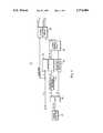
- FIG. 1is a block diagram representation of a pulse width modulation (PWM) circuit
- FIG. 2is a table of digital count words and corresponding reversed order count words
- FIG. 3Ashows exemplary outputs from the PWM circuit
- FIG. 3Bshows exemplary outputs from a conventional PWM circuit
- FIG. 4is a block diagram representation of an alternate PWM circuit
- FIG. 5is a flow diagram of a modulation process performed by the alternate PWM circuit.
- FIG. 1is a block diagram representation of a pulse width modulation (PWM) circuit 10 in accordance with the present invention.
- PWM circuit 10translates digital data input into an analog signal output, and may be used in numerous systems where such functionality is required.
- PWM circuit 10includes at least a digital counter 12, a significance reverser 14, and a comparator circuit 16.
- ASICapplication specific integrated circuit
- Counter 12is configured to produce a plurality of digital count words, each having at least two bits. Counter 12 sequentially counts from a first value (e.g., 0000) to a last value (e.g., 1111), preferably in a conventional manner. However, nothing requires counter 12 to count through all of the available bit combinations. Counter 12 may include any number of count bits, and PWM circuit 10 need not utilize all of the count bits generated by counter 12. As shown in FIG. 1, N bits from counter 12 are utilized by PWM circuit 10, where N ⁇ 2.
- a count cyclerefers to the time required for counter 12 to count from the first value to the last value. Consequently, the length of the count cycle in time is dependent upon the digital clock rate of PWM circuit 10 and the bit resolution of counter 12.
- Counter 12 and comparator 16may receive a common timing clock signal generated by an external timing reference (not shown).
- the output of counter 12is coupled to significance reverser 14, which reverses the relative order of significance of at least two of the digital count word bits.
- the digital count wordhas at least a first bit and a second bit, where the first bit is of higher significance relative to the second bit, and the significance reverser "rearranges" the first and second bits such that the second bit is of higher significance relative to the first bit.
- significance reverser 14reverses the order of significance of all of the digital count word bits. Each N-bit count word is reversed to produce an associated reversed order count word.
- significance reverser 14is realized by hard wiring the output of counter 12 to the input of comparator 16 in reverse order, i.e., the most significant bit (MSB) of a count word becomes the least significant bit (LSB) of a corresponding reversed order count word and the LSB of the count word becomes the MSB of the corresponding reversed order count word.
- significance reverser 14is preferably realized by a specific arrangement of electronic connections, it may be alternately realized by one or more discrete components if necessary.
- FIG. 2is a table of standard digital count words, exemplary reversed order count words, and the corresponding magnitudes of the standard and reversed order count words.
- the reversed order count words in FIG. 2are generated when all of the count word bits are reversed.
- the standard count sequenceproceeds from 0 to 15, as shown.
- the corresponding reversed order count sequenceproceeds as follows: 0, 8, 4, 12 . . . 11, 7, 15.
- FIG. 2shows how the standard count word bits are reversed to obtain the reversed order count words.
- Comparator 16is coupled to significance reverser 14 such that it receives the reversed order count words as a first input (labeled A). Comparator 16 also receives a digital input word as a second input (labeled B). In the preferred embodiment, the digital input word remains substantially constant during at least one count cycle.
- the digital input wordmay be generated in response to different operating parameters depending upon the specific application, and application-specific algorithms determine the current value of the input word. For example, a microprocessor in a digital data receiver can produce the digital input word in response to symbol tracking processes. PWM 10 may, in turn, translate the digital input word into an analog control signal that regulates a frequency reference.
- Comparator 16compares the magnitude of the reversed order count word to the magnitude of the digital input word using well known methodologies.
- comparator 16generates a high output value when the magnitude of the digital input word is greater than the magnitude of the reversed order count word, i.e., B>A, and otherwise generates a low output value.
- comparator 16may be configured to perform alternate mathematical operations to suit specific applications (e.g., B ⁇ A or A ⁇ B).
- the output signalincludes a number of pulses distributed substantially evenly in time during the count cycle.
- PWM 10may alternatively include one or more distinct elements (not shown) that function to produce the output signal in response to the above comparison.
- the digital input words and the reversed order count wordsinclude the same number of bits.
- the digital input wordsare configured to indicate a duty cycle for the analog output signal.
- duty cyclerefers to the ratio of the number of clock pulses having a high output to the total number of clock pulses in one count cycle.
- PWM circuit 10produces an analog output that approximately has the duty cycle indicated by the digital input word.
- FIG. 3Bshows a corresponding output from a conventional PWM system.
- the output from PWM circuit 10is indicated by the reference number 18 (FIG. 2A) and the conventional PWM output is indicated by the reference number 20 (FIG. 3B).
- PWM circuit 10produces a high output value whenever the magnitude of the reversed order count word is less than eleven. Consequently, the analog output is at a high level for eleven clock pulses, and the output pulses are distributed substantially evenly in time during the count cycle.
- the conventional PWM outputis high for the first eleven clock pulses and low for the remaining five clock pulses.
- PWM circuit 10produces more high level output pulses during the count cycle. Regardless of the input value, PWM circuit 10 preferably maintains the spaced distribution of the output pulses as much as possible. In contrast, conventional PWM circuits produce only one output pulse per counter cycle.
- PWM circuit 10also reduces the amount of transport delay associated with the output signal. In other words, the average output level settles to an acceptable level early in the count cycle.
- the average value of output 18 taken over the first two clock pulsesis 2/2 (two output high pulses for two clock pulses).
- the corresponding error between this average value and the desired output value of 11/16is 5/16.
- the average output value taken over four clock pulsesis 12/16, and the corresponding error is only 1/16.
- the corresponding error after the eighth and sixteenth clock pulsesis 1/16 and zero, respectively.
- the error after two, four, eight, and sixteen clock pulses for the conventional PWM output 20(FIG. 3B) is 5/16, 5/16, 5/16, and zero, respectively.
- PWM circuit 22is configured such that the output gain of the analog signal is variable.
- a programmable output gainis desirable where a system switches between the output of PWM circuit 22 (which may have a high gain due to a high data rate) and the output of a second control circuit having a comparatively low gain.
- PWM 22includes an output interface for compatibility with conventional phase/frequency detector (PFD) output configurations.
- PWM circuit 22includes a digital counter 24 configured to produce digital count words having at least (N+M) bits.
- the output of counter 24is coupled to a multiplexer circuit (MUX) 26, which separates each digital count word into a first word and a second word.
- MUX 26is configured such that the value of M and/or the value of N is selectable via a control signal (not shown). It should be appreciated that the value of M may be selected and set according to anticipated system characteristics or periodically updated as necessary.
- the first wordincludes N bits of higher significance relative to the digital count word and the second word includes M bits of lower significance relative to the digital count word.
- the first wordserves as an input to a significance reverser 28 and the second word serves as an input to a magnitude detector 30 (described below).
- Significance reverser 28performs the same function as significance reverser 14 (described above in connection with FIG. 1).
- the output of significance reverser 28is coupled to a comparator circuit 32, which receives the N-bit reversed order count words as a first input (labeled A).
- Comparator 32also receives N bits from a digital input word as a second input (labeled B).
- the digital input wordincludes (N+1) bits, and the MSB of the digital input word is isolated for input into an output selection circuit 34 (described below). As such, the N remaining bits are utilized by comparator 32.
- the operation of comparator 32is similar to the operation of comparator 16, and comparator 32 produces a pulsed analog output in the manner described above.
- the output of comparator 32is coupled to an output control circuit 36.
- the output of magnitude detector 30is also coupled to output control circuit 36.
- Magnitude detector 30is configured to detect when the magnitude of the M-bit second word equals a predetermined value, e.g., zero in the preferred embodiment.
- Magnitude detector 30employs digital logic techniques known to those skilled in the art.
- Magnitude detector 30preferably produces a logic high output when the magnitude of the second word equals the predetermined value and produces a logic low output when the magnitude of the second word differs from the predetermined value.
- Output control circuit 36is configured to pass the analog output from comparator 32 when it receives a logic high signal from magnitude detector 30. When the magnitude of the second word differs from the predetermined value, output control circuit 36 withholds the analog output.
- the preferred embodimentutilizes a logic AND gate.
- MUX 26, magnitude detector 30, and output control circuit 36cooperate to control the gain of the analog output signal.
- output control circuit 36will provide the analog output to selection circuit 34 after a given number of clock pulses.
- the gain of the analog outputis effectively reduced by a factor of 2 M by distributing the high output values over the longer extended count cycle.
- Output control circuit 36is coupled to selection circuit 34.
- Selection circuit 34is configured to mimic conventional PFD outputs, which typically include PUMP UP and PUMP DOWN outputs that drive one or more charge pumps.
- PFD outputstypically include PUMP UP and PUMP DOWN outputs that drive one or more charge pumps.
- selection circuit 34may be alternatively configured according to specific system requirements.
- Selection circuit 34provides the analog signal to one of a plurality of output points (labeled OUTPUT1 and OUTPUT2) in response to the MSB of the digital input word. As discussed above, the MSB is isolated and routed to selection circuit 34. In the preferred embodiment, the MSB functions as a sign bit, and its value determines whether the analog signal is provided to OUTPUT1 or OUTPUT2. Depending upon specific system requirements, OUTPUT1 and OUTPUT2 may be configured to drive a differential charge pump or a single ended charge pump. Those skilled in the art will recognize that selection circuit 34 may include conventional switches, multiplexers, or other digital components.
- a modulation process 38 performed by PWM circuit 22is illustrated as a flow diagram.
- Process 38is preferably performed after a desired value for M has been selected to adjust the output gain of PWM circuit 22.
- process 38is described herein as it applies to a single digital count word established during one clock pulse. Those skilled in the art will realize that process 38 is repeated as counter 24 sequentially counts through the count cycle.
- the digital input wordmay be updated after completion of at least one count cycle.
- Modulation process 38begins with a task 40, which obtains the current digital input word and the current digital count word.
- the input wordmay be generated by a digital microprocessor according to system specifications, and the count word is generated by counter 24 (see FIG. 4).
- a task 42truncates the input word and isolates the MSB of the input word.
- Task 42may be inherently performed by PWM circuit 22, depending upon how the various digital components are arranged and interconnected.
- a task 44separates the count word bits into a first word having at least two bits and a second word.
- MUX 26(or an equivalently functioning circuit) performs task 44.
- Task 44is preferably responsive to the value of M previously selected.
- the first wordpreferably includes N higher order bits and the second word preferably includes M lower order bits, where counter 24 generates words having at least (N+M) bits.
- a task 46reverses the order of significance of at least two (and preferably all) of the bits in the first word. As described above, significance reverser 28 performs task 46. Task 46 transforms the first word into a reversed order count word having N bits. Following task 46, a query task 48 is initiated.
- Query task 48is preferably performed by comparator 32, which determines whether the magnitude of the truncated input word is greater than the magnitude of the reversed order count word. If query task 48 determines that the magnitude of the truncated input word exceeds the magnitude of the reversed order count word, then a task 50 generates a first analog value for the output. If query task 48 determines otherwise, then a task 52 generates a second analog value for the output. In the preferred embodiment, the first and second values correspond to high and low values, respectively.
- magnitude detector 30performs a query task 54 to determine whether the magnitude of the second word equals a predetermined value.
- a predetermined valuecan be selected according to individual applications, the preferred embodiment uses zero as a convenient value. If query task 54 determines that the magnitude of the second word equals the predetermined value, then a task 56 provides the high or low value as an output. If, however, the magnitude of the second word differs from the predetermined value, then a task 58 withholds the output. Tasks 58 and 60 are preferably performed by output control circuit 36 (described above).
- Query task 60, task 62, and task 64are performed by output selection circuit 34.
- the MSBis utilized as a sign bit and the two output channels of output selection circuit 34 are configured to mimic the output interface of a conventional phase/frequency detector circuit. For example, one output channel can provide a positive drive signal (pump up) to a charge pump and the other output channel can provide a negative drive signal (pump down) to the charge pump.
- the negative drive signalcan be realized by inverting the output according to known techniques.
- modulation process 38ends. As discussed above, process 38 is preferably repeated for each count word generated by counter 24. As process 38 is repeated during the count cycle of counter 24, PWM circuit 22 produces an analog signal having a number of high output pulses evenly spread during the count cycle. The digital input value (which controls the duty cycle of the analog output) may be updated at a rate approximately equal to one count cycle or an integral multiple thereof.
- the present inventionprovides an improved digital PWM circuit that translates digital data into an analog signal.
- the PWM circuitis easy to implement in an all-digital environment and economical to use in systems that process both digital and analog signals.
- the improved PWM circuitgenerates less harmonic components near its digital counter update frequency.
- a PWM circuit according to the present inventionproduces an analog signal having an average output level that can be adequately determined early in the digital counter cycle.
- a PWM circuit according to a preferred embodiment of the present inventionmay be programmed such that the output gain approximates the output gain of an external circuit.
Landscapes
- Engineering & Computer Science (AREA)
- Theoretical Computer Science (AREA)
- Physics & Mathematics (AREA)
- General Engineering & Computer Science (AREA)
- General Physics & Mathematics (AREA)
- Analogue/Digital Conversion (AREA)
Abstract
Description
Claims (17)
Priority Applications (1)
| Application Number | Priority Date | Filing Date | Title |
|---|---|---|---|
| US08/627,930US5774084A (en) | 1996-04-03 | 1996-04-03 | Method and apparatus for translating digital data into an analog signal |
Applications Claiming Priority (1)
| Application Number | Priority Date | Filing Date | Title |
|---|---|---|---|
| US08/627,930US5774084A (en) | 1996-04-03 | 1996-04-03 | Method and apparatus for translating digital data into an analog signal |
Publications (1)
| Publication Number | Publication Date |
|---|---|
| US5774084Atrue US5774084A (en) | 1998-06-30 |
Family
ID=24516715
Family Applications (1)
| Application Number | Title | Priority Date | Filing Date |
|---|---|---|---|
| US08/627,930Expired - LifetimeUS5774084A (en) | 1996-04-03 | 1996-04-03 | Method and apparatus for translating digital data into an analog signal |
Country Status (1)
| Country | Link |
|---|---|
| US (1) | US5774084A (en) |
Cited By (27)
| Publication number | Priority date | Publication date | Assignee | Title |
|---|---|---|---|---|
| US6038265A (en)* | 1997-04-21 | 2000-03-14 | Motorola, Inc. | Apparatus for amplifying a signal using digital pulse width modulators |
| US6133858A (en)* | 1996-10-21 | 2000-10-17 | Robert Bosch Gmbh | Bus system, a peripheral device and a method for decoding a digital signal |
| US6172633B1 (en)* | 1999-09-24 | 2001-01-09 | Lsi Logic Corporation | Enhanced pulse width modulator |
| US6199290B1 (en) | 1999-07-30 | 2001-03-13 | Excellon Automation Co. | Method and apparatus for automatic loading and registration of PCBs |
| US6281822B1 (en)* | 1999-05-28 | 2001-08-28 | Dot Wireless, Inc. | Pulse density modulator with improved pulse distribution |
| US6435037B1 (en) | 2000-01-06 | 2002-08-20 | Data Sciences International, Inc. | Multiplexed phase detector |
| US6459398B1 (en) | 1999-07-20 | 2002-10-01 | D.S.P.C. Technologies Ltd. | Pulse modulated digital to analog converter (DAC) |
| US20020180589A1 (en)* | 2001-05-30 | 2002-12-05 | Gabara Thaddeus John | Comparator circuits having non-complementary input structures |
| US6539316B1 (en) | 2000-01-06 | 2003-03-25 | Data Sciences International, Inc. | Phase detector |
| US6595071B1 (en) | 2000-01-06 | 2003-07-22 | Transoma Medical, Inc. | Estimation of error angle in ultrasound flow measurement |
| US6856269B1 (en)* | 2004-05-13 | 2005-02-15 | Winbond Electronics Corp. | D/A conversion method and D/A converter |
| EP1575171A1 (en)* | 2004-03-10 | 2005-09-14 | Patent-Treuhand-Gesellschaft für elektrische Glühlampen mbH | Digital/analog conversion with an interleaved pulse width modulated signal |
| US20050231410A1 (en)* | 2004-04-16 | 2005-10-20 | Lee Ying L | Schemes to implement multi-level PWM in digital system |
| US7079589B1 (en)* | 2002-06-10 | 2006-07-18 | National Semiconductor Corporation | Serial digital communication superimposed on a digital signal over a single wire |
| US20080049850A1 (en)* | 2002-06-21 | 2008-02-28 | Stefanos Sidiropoulos | Methods And Apparatus For Clock And Data Recovery Using Transmission Lines |
| US20080055142A1 (en)* | 2004-09-27 | 2008-03-06 | Stephen Deleu | Electronic Filter Device for the Reception of TV Signals |
| US20080111715A1 (en)* | 2006-11-15 | 2008-05-15 | Fujitsu Limited | Serial data receiving circuit and serial data receiving method |
| US20080260071A1 (en)* | 2005-12-07 | 2008-10-23 | Stefanos Sidiropoulos | Methods and Apparatus for Frequency Synthesis with Feedback Interpolation |
| US7855669B2 (en) | 2008-09-26 | 2010-12-21 | Silicon Laboratories, Inc. | Circuit device to generate a high precision control signal |
| US20110103417A1 (en)* | 2005-03-04 | 2011-05-05 | Stefanos Sidiropoulos | Systems, Methods, and Circuits for Driving Large Off-Chip Loads |
| US20110228889A1 (en)* | 2010-03-19 | 2011-09-22 | Dean Liu | Repeater Architecture with Single Clock Multiplier Unit |
| US8700944B2 (en) | 2010-03-19 | 2014-04-15 | Netlogic Microsystems, Inc. | Programmable drive strength in memory signaling |
| US9041375B2 (en) | 2012-10-30 | 2015-05-26 | Infineon Technologies Ag | High resolution control for a multimode SMPS converter and high resolution slope generator |
| US11381224B2 (en) | 2018-06-08 | 2022-07-05 | Southern Research Institute | Clockless programmable pulse width generation using an inverse chaotic map |
| US11415947B2 (en)* | 2018-06-08 | 2022-08-16 | Kratos Sre, Inc. | Clockless time-to-digital converter |
| US11733364B2 (en) | 2020-05-21 | 2023-08-22 | Kratos Sre, Inc. | Target ranging with subsampled noise correlation |
| US11811954B2 (en) | 2018-06-08 | 2023-11-07 | Kratos Sre, Inc. | Physically unclonable functions using pulse width chaotic maps |
Citations (3)
| Publication number | Priority date | Publication date | Assignee | Title |
|---|---|---|---|---|
| US3836908A (en)* | 1973-04-10 | 1974-09-17 | Grundig Emv | Digital to analog converter |
| US5062105A (en)* | 1990-01-02 | 1991-10-29 | At&T Bell Laboratories | Programmable multiplexing techniques for mapping a capacity domain into a time domain within a frame |
| US5337338A (en)* | 1993-02-01 | 1994-08-09 | Qualcomm Incorporated | Pulse density modulation circuit (parallel to serial) comparing in a nonsequential bit order |
- 1996
- 1996-04-03USUS08/627,930patent/US5774084A/ennot_activeExpired - Lifetime
Patent Citations (3)
| Publication number | Priority date | Publication date | Assignee | Title |
|---|---|---|---|---|
| US3836908A (en)* | 1973-04-10 | 1974-09-17 | Grundig Emv | Digital to analog converter |
| US5062105A (en)* | 1990-01-02 | 1991-10-29 | At&T Bell Laboratories | Programmable multiplexing techniques for mapping a capacity domain into a time domain within a frame |
| US5337338A (en)* | 1993-02-01 | 1994-08-09 | Qualcomm Incorporated | Pulse density modulation circuit (parallel to serial) comparing in a nonsequential bit order |
Cited By (43)
| Publication number | Priority date | Publication date | Assignee | Title |
|---|---|---|---|---|
| US6133858A (en)* | 1996-10-21 | 2000-10-17 | Robert Bosch Gmbh | Bus system, a peripheral device and a method for decoding a digital signal |
| US6038265A (en)* | 1997-04-21 | 2000-03-14 | Motorola, Inc. | Apparatus for amplifying a signal using digital pulse width modulators |
| US6281822B1 (en)* | 1999-05-28 | 2001-08-28 | Dot Wireless, Inc. | Pulse density modulator with improved pulse distribution |
| US6459398B1 (en) | 1999-07-20 | 2002-10-01 | D.S.P.C. Technologies Ltd. | Pulse modulated digital to analog converter (DAC) |
| US6199290B1 (en) | 1999-07-30 | 2001-03-13 | Excellon Automation Co. | Method and apparatus for automatic loading and registration of PCBs |
| US6172633B1 (en)* | 1999-09-24 | 2001-01-09 | Lsi Logic Corporation | Enhanced pulse width modulator |
| US6435037B1 (en) | 2000-01-06 | 2002-08-20 | Data Sciences International, Inc. | Multiplexed phase detector |
| US6539316B1 (en) | 2000-01-06 | 2003-03-25 | Data Sciences International, Inc. | Phase detector |
| US6595071B1 (en) | 2000-01-06 | 2003-07-22 | Transoma Medical, Inc. | Estimation of error angle in ultrasound flow measurement |
| US20020180589A1 (en)* | 2001-05-30 | 2002-12-05 | Gabara Thaddeus John | Comparator circuits having non-complementary input structures |
| US6930516B2 (en)* | 2001-05-30 | 2005-08-16 | Agere Systems Inc. | Comparator circuits having non-complementary input structures |
| US7079589B1 (en)* | 2002-06-10 | 2006-07-18 | National Semiconductor Corporation | Serial digital communication superimposed on a digital signal over a single wire |
| US20080049850A1 (en)* | 2002-06-21 | 2008-02-28 | Stefanos Sidiropoulos | Methods And Apparatus For Clock And Data Recovery Using Transmission Lines |
| US8155236B1 (en) | 2002-06-21 | 2012-04-10 | Netlogic Microsystems, Inc. | Methods and apparatus for clock and data recovery using transmission lines |
| US8102936B2 (en) | 2002-06-21 | 2012-01-24 | Netlogic Microsystems, Inc. | Methods and apparatus for clock and data recovery using transmission lines |
| US8599983B2 (en) | 2002-06-21 | 2013-12-03 | Netlogic Microsystems, Inc. | Methods and apparatus for clock and data recovery using transmission lines |
| EP1575171A1 (en)* | 2004-03-10 | 2005-09-14 | Patent-Treuhand-Gesellschaft für elektrische Glühlampen mbH | Digital/analog conversion with an interleaved pulse width modulated signal |
| US7197683B2 (en) | 2004-03-10 | 2007-03-27 | Patent-Treuhand-Gesellschaft Fur Elektrisch Gluhlampen Mbh | Digital-to-analog conversion with an interleaved, pulse-width modulated signal |
| US20050206544A1 (en)* | 2004-03-10 | 2005-09-22 | Patent-Treuhand-Gesellschaft Fur Elektrische Gluhlampen Mbh | Digital-to-analog conversion with an interleaved, pulse-width modulated signal |
| US20050231410A1 (en)* | 2004-04-16 | 2005-10-20 | Lee Ying L | Schemes to implement multi-level PWM in digital system |
| US7215272B2 (en)* | 2004-04-16 | 2007-05-08 | Ying Lau Lee | Schemes to implement multi-level PWM in digital system |
| US6856269B1 (en)* | 2004-05-13 | 2005-02-15 | Winbond Electronics Corp. | D/A conversion method and D/A converter |
| US20080055142A1 (en)* | 2004-09-27 | 2008-03-06 | Stephen Deleu | Electronic Filter Device for the Reception of TV Signals |
| US7541957B2 (en)* | 2004-09-27 | 2009-06-02 | Unitron | Electronic filter device for the reception of TV signals |
| US8369369B2 (en)* | 2005-03-04 | 2013-02-05 | Netlogic Microsystems, Inc. | Systems, methods, and circuits for driving large off-chip loads |
| US20110103417A1 (en)* | 2005-03-04 | 2011-05-05 | Stefanos Sidiropoulos | Systems, Methods, and Circuits for Driving Large Off-Chip Loads |
| US8433018B2 (en) | 2005-12-07 | 2013-04-30 | Netlogic Microsystems, Inc. | Methods and apparatus for frequency synthesis with feedback interpolation |
| US20080260071A1 (en)* | 2005-12-07 | 2008-10-23 | Stefanos Sidiropoulos | Methods and Apparatus for Frequency Synthesis with Feedback Interpolation |
| US8667038B1 (en) | 2005-12-07 | 2014-03-04 | Netlogic Microsystems, Inc. | Methods and apparatus to increase the resolution of a clock synthesis circuit that uses feedback interpolation |
| US7528748B2 (en)* | 2006-11-15 | 2009-05-05 | Fujitsu Microelectronics Limited | Serial data receiving circuit and serial data receiving method |
| US20080111715A1 (en)* | 2006-11-15 | 2008-05-15 | Fujitsu Limited | Serial data receiving circuit and serial data receiving method |
| US7855669B2 (en) | 2008-09-26 | 2010-12-21 | Silicon Laboratories, Inc. | Circuit device to generate a high precision control signal |
| US20110228889A1 (en)* | 2010-03-19 | 2011-09-22 | Dean Liu | Repeater Architecture with Single Clock Multiplier Unit |
| US8638896B2 (en) | 2010-03-19 | 2014-01-28 | Netlogic Microsystems, Inc. | Repeate architecture with single clock multiplier unit |
| US8700944B2 (en) | 2010-03-19 | 2014-04-15 | Netlogic Microsystems, Inc. | Programmable drive strength in memory signaling |
| US9041375B2 (en) | 2012-10-30 | 2015-05-26 | Infineon Technologies Ag | High resolution control for a multimode SMPS converter and high resolution slope generator |
| US11381224B2 (en) | 2018-06-08 | 2022-07-05 | Southern Research Institute | Clockless programmable pulse width generation using an inverse chaotic map |
| US11415947B2 (en)* | 2018-06-08 | 2022-08-16 | Kratos Sre, Inc. | Clockless time-to-digital converter |
| US11726433B2 (en) | 2018-06-08 | 2023-08-15 | Kratos Sre, Inc. | Clockless time-to-digital converter |
| US11811954B2 (en) | 2018-06-08 | 2023-11-07 | Kratos Sre, Inc. | Physically unclonable functions using pulse width chaotic maps |
| US12028069B2 (en) | 2018-06-08 | 2024-07-02 | Kratos Sre, Inc. | Clockless pulse width generation |
| US12301738B2 (en) | 2018-06-08 | 2025-05-13 | Kratos Sre, Inc. | Physically unclonable functions using pulse width chaotic maps |
| US11733364B2 (en) | 2020-05-21 | 2023-08-22 | Kratos Sre, Inc. | Target ranging with subsampled noise correlation |
Similar Documents
| Publication | Publication Date | Title |
|---|---|---|
| US5774084A (en) | Method and apparatus for translating digital data into an analog signal | |
| US7439787B2 (en) | Methods and apparatus for a digital pulse width modulator using multiple delay locked loops | |
| US5038117A (en) | Multiple-modulator fractional-N divider | |
| CN1447935B (en) | Method for generating clock signal and clock generator | |
| JPH11234129A (en) | Frequency synthesizer and method therefor | |
| EP1368896A1 (en) | Sigma delta fractional-n frequency divider with improved noise and spur performance | |
| US11804847B2 (en) | Fractional frequency synthesis by sigma-delta modulating frequency of a reference clock | |
| CN110048714A (en) | Synthesizer and phase-frequency detector | |
| EP0479969A1 (en) | SYNTHESIZER WITH BROKEN PART RATIO FOR A VOICE / DATA COMMUNICATION SYSTEM. | |
| US6850177B2 (en) | Digital to analog convertor | |
| US7327820B2 (en) | Method and apparatus for reducing quantization noise in fractional-N frequency synthesizers | |
| US6914935B2 (en) | Fractional N synthesizer with reduced fractionalization spurs | |
| EP0438867B1 (en) | Multiple-modulator fractional-N divider | |
| US6693987B1 (en) | Digital-to-analog DAC-driven phase-locked loop PLL with slave PLL's driving DAC reference voltages | |
| AU612297B2 (en) | Voltage controlled oscillator | |
| CN1455983A (en) | Frequency synthesizer | |
| EP0162496B1 (en) | Phase-locked loop with switchable phase detector | |
| AU3847500A (en) | Improvements relating to frequency synthesisers | |
| US5050195A (en) | Narrow range digital clock circuit | |
| US20020184274A1 (en) | Sinusoid synthesis | |
| US20240039521A1 (en) | Fractional divider-calibrated phase modulator and interpolator for a wireless transmitter | |
| EP1177633A1 (en) | Nested modulator arrangement | |
| SU1730719A1 (en) | Digital frequency synthesizer | |
| CA1304457C (en) | Narrow range digital clock circuit | |
| SU1149394A1 (en) | Digital phase discriminator |
Legal Events
| Date | Code | Title | Description |
|---|---|---|---|
| AS | Assignment | Owner name:SICOM, INC., ARIZONA Free format text:ASSIGNMENT OF ASSIGNORS INTEREST;ASSIGNORS:BROMBAUGH, ERIC MARTIN;LIEBETREU, JOHN MICHAEL;MCCALLISTER, RONALD DUANE;REEL/FRAME:007957/0279 Effective date:19960329 | |
| STCF | Information on status: patent grant | Free format text:PATENTED CASE | |
| CC | Certificate of correction | ||
| AS | Assignment | Owner name:SICOM, INC., A DELAWARE CORPORATION, ARIZONA Free format text:ASSIGNMENT OF ASSIGNORS INTEREST;ASSIGNORS:BROMBAUGH, ERIC MARTIN;LIEBETREU, JOHN MICHAEL;MCCALLISTER, RONALD DUANE;REEL/FRAME:011164/0364;SIGNING DATES FROM 19960327 TO 19960329 | |
| FEPP | Fee payment procedure | Free format text:PAT HOLDER NO LONGER CLAIMS SMALL ENTITY STATUS, ENTITY STATUS SET TO UNDISCOUNTED (ORIGINAL EVENT CODE: STOL); ENTITY STATUS OF PATENT OWNER: LARGE ENTITY | |
| FEPP | Fee payment procedure | Free format text:PAYOR NUMBER ASSIGNED (ORIGINAL EVENT CODE: ASPN); ENTITY STATUS OF PATENT OWNER: LARGE ENTITY | |
| FEPP | Fee payment procedure | Free format text:ENTITY STATUS SET TO UNDISCOUNTED (ORIGINAL EVENT CODE: BIG.); ENTITY STATUS OF PATENT OWNER: LARGE ENTITY | |
| FPAY | Fee payment | Year of fee payment:4 | |
| REMI | Maintenance fee reminder mailed | ||
| AS | Assignment | Owner name:INTERSIL AMERICAS, INC., CALIFORNIA Free format text:ASSIGNMENT OF ASSIGNORS INTEREST;ASSIGNOR:SICOM, INC.;REEL/FRAME:014446/0738 Effective date:20030826 | |
| FPAY | Fee payment | Year of fee payment:8 | |
| FPAY | Fee payment | Year of fee payment:12 | |
| AS | Assignment | Owner name:MORGAN STANLEY & CO. INCORPORATED,NEW YORK Free format text:SECURITY AGREEMENT;ASSIGNORS:INTERSIL CORPORATION;TECHWELL, INC.;INTERSIL COMMUNICATIONS, INC.;AND OTHERS;REEL/FRAME:024320/0001 Effective date:20100427 Owner name:MORGAN STANLEY & CO. INCORPORATED, NEW YORK Free format text:SECURITY AGREEMENT;ASSIGNORS:INTERSIL CORPORATION;TECHWELL, INC.;INTERSIL COMMUNICATIONS, INC.;AND OTHERS;REEL/FRAME:024320/0001 Effective date:20100427 |