US5774022A - Digital clock recovery loop - Google Patents
Digital clock recovery loopDownload PDFInfo
- Publication number
- US5774022A US5774022AUS08/707,220US70722096AUS5774022AUS 5774022 AUS5774022 AUS 5774022AUS 70722096 AUS70722096 AUS 70722096AUS 5774022 AUS5774022 AUS 5774022A
- Authority
- US
- United States
- Prior art keywords
- controlled oscillator
- voltage
- voltage controlled
- control node
- frequency
- Prior art date
- Legal status (The legal status is an assumption and is not a legal conclusion. Google has not performed a legal analysis and makes no representation as to the accuracy of the status listed.)
- Expired - Lifetime
Links
- 238000011084recoveryMethods0.000titleclaimsabstractdescription36
- 230000008859changeEffects0.000claimsabstractdescription11
- 239000000284extractSubstances0.000claimsabstract4
- 230000007704transitionEffects0.000claimsdescription21
- 238000001228spectrumMethods0.000claimsdescription4
- 238000001514detection methodMethods0.000abstractdescription6
- 238000010586diagramMethods0.000description16
- 239000003990capacitorSubstances0.000description6
- 230000006870functionEffects0.000description6
- 238000000034methodMethods0.000description6
- 238000013461designMethods0.000description4
- 230000008569processEffects0.000description3
- 238000012905input functionMethods0.000description2
- 238000013459approachMethods0.000description1
- 230000000694effectsEffects0.000description1
- 238000012986modificationMethods0.000description1
- 230000004048modificationEffects0.000description1
- 230000010355oscillationEffects0.000description1
- 238000012545processingMethods0.000description1
- 238000005070samplingMethods0.000description1
- 238000000926separation methodMethods0.000description1
Images


Classifications
- H—ELECTRICITY
- H03—ELECTRONIC CIRCUITRY
- H03L—AUTOMATIC CONTROL, STARTING, SYNCHRONISATION OR STABILISATION OF GENERATORS OF ELECTRONIC OSCILLATIONS OR PULSES
- H03L7/00—Automatic control of frequency or phase; Synchronisation
- H03L7/06—Automatic control of frequency or phase; Synchronisation using a reference signal applied to a frequency- or phase-locked loop
- H03L7/08—Details of the phase-locked loop
- H03L7/10—Details of the phase-locked loop for assuring initial synchronisation or for broadening the capture range
- H03L7/113—Details of the phase-locked loop for assuring initial synchronisation or for broadening the capture range using frequency discriminator
- H—ELECTRICITY
- H03—ELECTRONIC CIRCUITRY
- H03L—AUTOMATIC CONTROL, STARTING, SYNCHRONISATION OR STABILISATION OF GENERATORS OF ELECTRONIC OSCILLATIONS OR PULSES
- H03L7/00—Automatic control of frequency or phase; Synchronisation
- H03L7/06—Automatic control of frequency or phase; Synchronisation using a reference signal applied to a frequency- or phase-locked loop
- H03L7/08—Details of the phase-locked loop
- H03L7/085—Details of the phase-locked loop concerning mainly the frequency- or phase-detection arrangement including the filtering or amplification of its output signal
- H03L7/089—Details of the phase-locked loop concerning mainly the frequency- or phase-detection arrangement including the filtering or amplification of its output signal the phase or frequency detector generating up-down pulses
- H03L7/0891—Details of the phase-locked loop concerning mainly the frequency- or phase-detection arrangement including the filtering or amplification of its output signal the phase or frequency detector generating up-down pulses the up-down pulses controlling source and sink current generators, e.g. a charge pump
- H03L7/0895—Details of the current generators
- H03L7/0896—Details of the current generators the current generators being controlled by differential up-down pulses
- H—ELECTRICITY
- H04—ELECTRIC COMMUNICATION TECHNIQUE
- H04L—TRANSMISSION OF DIGITAL INFORMATION, e.g. TELEGRAPHIC COMMUNICATION
- H04L7/00—Arrangements for synchronising receiver with transmitter
- H04L7/02—Speed or phase control by the received code signals, the signals containing no special synchronisation information
- H04L7/033—Speed or phase control by the received code signals, the signals containing no special synchronisation information using the transitions of the received signal to control the phase of the synchronising-signal-generating means, e.g. using a phase-locked loop
- H—ELECTRICITY
- H04—ELECTRIC COMMUNICATION TECHNIQUE
- H04B—TRANSMISSION
- H04B1/00—Details of transmission systems, not covered by a single one of groups H04B3/00 - H04B13/00; Details of transmission systems not characterised by the medium used for transmission
- H04B1/69—Spread spectrum techniques
- H04B1/707—Spread spectrum techniques using direct sequence modulation
Definitions
- This inventionrelates to communications systems. More particularly, the invention relates to phase locked loops employed in communications systems.
- phase locked loopsare known in the art.
- a phase locked loopis a circuit containing an oscillator whose output phase and/or frequency is steered to keep it in synchronization with some reference signal.
- a phase locked looptypically includes a phase comparator having a first input receiving an input reference signal, having a second input, and having an output, a filter having an input receiving the output of the phase comparator and having an output, an amplifier having an input receiving the output of the filter, and having an output defining the output of the phase locked loop, and a voltage controlled oscillator having an input receiving a control voltage from the amplifier and having an output connected to the second input of the phase comparator.
- Phase locked loopshave various applications. In many communications systems, for example, it is necessary to recover a clock signal from the received data. A phase locked loop is one way of recovering such a clock signal.
- the inventionprovides a digital clock recovery loop.
- the digital clock recovery loopincludes a voltage controlled oscillator.
- the voltage controlled oscillatorhas an output, and produces a square wave at output having a frequency controlled by the voltage on an input control node.
- only one control nodeis employed; however, the illustrated embodiment, a differential control node scheme is employed involving two control nodes. Therefore, in the illustrated embodiment, a capacitor is provided on each control node, and control voltages are stored in analog form on these two capacitors.
- the frequency at outputis at least one half of the final recovered frequency and not greater than the final recovered frequency. The output frequency rises monotonically, nearly linearly, as the control node voltage is increased.
- the digital clock recovery loopfurther includes a charge pump and loop filters which control the rate of change of the voltage on the control node of the voltage controlled oscillator.
- the digital clock recovery loopfurther includes a start-up circuit which performs frequency detection when the voltage controlled oscillator first starts up and, in conjunction with the charge pump and loop filters, causes the voltage on the control node of the voltage controlled oscillator to change rapidly.
- the digital clock recovery loopfurther includes a state machine which performs phase detection when the frequency of the voltage controlled oscillator is within a few percent of its final value and, in conjunction with the charge pump and loop filters, causes the voltage on the control node of the voltage controlled oscillator to change slowly.
- the only analog blocksare the voltage controlled oscillator and the charge pump.
- the rest of the circuits of the digital clock recovery loopare digital circuits which are easy to build at high yield in integrated circuit processes.
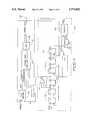
- FIG. 1is a circuit diagram of a digital clock recovery loop embodying the invention.
- FIG. 2is a plot of frequency produced by a voltage controlled oscillator versus control voltage applied to the voltage controlled oscillator.
- FIG. 3is a timing diagram showing when the start-up circuit of FIG. 1 issues pump up signals to increase the control voltage applied to the voltage controlled oscillator.
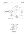
- FIG. 4is a state diagram illustrating the design of the state machine of FIG. 1.
- FIGS. 5-10illustrate steps used in designing a state machine that implements the state diagram of FIG. 4.
- FIG. 5illustrates flip-flops having outputs representing in binary form the various states of the state diagrams and having inputs representing next state values.
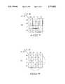
- FIG. 6is a state table.
- FIGS. 7 and 8are Karnaugh maps used to derive minimum logic circuitry needed to derive circuit output functions and flip-flop input functions.
- FIGS. 9 and 10illustrate logic circuitry that implements the state machine.
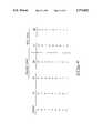
- FIG. 11is a simplified timing diagram illustrating operation of the state machine.
- FIG. 12is a table illustrating step sizes produced by the start-up circuit and the state machine.
- FIG. 13is a circuit diagram, in block diagram form, of a voltage controlled oscillator.
- FIGS. 14A and 14Bprovide a circuit diagram of charge pumps and loop filters.
- FIG. 15illustrates logic circuitry that is also employed to implement the state machine.
- phase locked loopIn many communications systems it is necessary to recover a clock signal from the received digital data stream. Typically, a phase locked loop of some type is used to extract the clock.
- phase locked loopis intended to indicate structure, not a state of operation (such as a loop that has achieved frequency lock).
- phase locked loopused to recover a clock signal from the received digital data stream.
- phase locked loopmust acquire the desired frequency without locking to a multiple or sub-multiple of the desired frequency; the phase locked loop must lock to the desired frequency within a certain time of interest; and the phase locked loop must yield consistent performance despite wide variation in device parameters which is inherent in integrated circuit processing.
- the phase locked loop employed in the illustrated embodimentsatisfies these requirements.
- the received digital data streamis encoded for direct sequence spread spectrum.
- a data bit "1"is represented by a thirty-one chip sequence and a data bit "0" is represented by the logical inversion of the same thirty-one chip sequence.
- Other forms of digital encodingcan be employed.
- FIG. 1shows a digital clock recovery loop 700 embodying the invention.
- the digital clock recovery loop 700comprises several sub-circuits.
- the digital clock recovery loop 700includes a voltage controlled oscillator 702.
- the voltage controlled oscillator 702has an output 704, and produces a square wave at output 704 having a frequency controlled by the voltage on an input control node.
- only one control nodeis employed; however, in the illustrated embodiment, a differential control node scheme is employed involving two control nodes "OUTN" and "OUTP" (see FIGS. 14A-B). Therefore, in the illustrated embodiment, a capacitor is provided on each control node, and control voltages are stored in analog form on these two capacitors.
- FIG. 2illustrates the frequency produced at the output 704 of the voltage controlled oscillator 702 relative to a voltage at the input control node.
- the digital clock recovery loop 700further includes a charge pump and loop filters which control the rate of change of the voltage on the control node of the voltage controlled oscillator.
- the charge pump and loop filtersare designated in FIG. 1 with reference numeral 706.
- the digital clock recovery loop 700further includes a start-up circuit 708 which performs frequency detection when the voltage controlled oscillator first starts up and, in conjunction with the charge pump and loop filters 706, causes the voltage on the control node of the voltage controlled oscillator to change rapidly.
- the digital clock recovery loop 700further includes a state machine 710 which performs phase detection when the frequency of the voltage controlled oscillator is within a few percent of its final value and, in conjunction with the charge pump and loop filters, causes the voltage on the control node of the voltage controlled oscillator 702 to change slowly.
- a state machine 710which performs phase detection when the frequency of the voltage controlled oscillator is within a few percent of its final value and, in conjunction with the charge pump and loop filters, causes the voltage on the control node of the voltage controlled oscillator 702 to change slowly.
- the only analog blocksare the voltage controlled oscillator 702 and the charge pump.
- the rest of the circuits of the digital clock recovery loopare digital circuits which are easy to build at high yield in integrated circuit processes.
- the digital clock recovery loopcauses the frequency at the output of the voltage controlled oscillator to vary until a predetermined number of this clock fit within the time interval of an identifiable discrete segment of the incoming data. More particularly, in the illustrated embodiment, the digital clock recovery loop causes the frequency at the output of the voltage controlled oscillator to increase until exactly four cycles of the clock fit within the time interval of a single direct spread spectrum chip. In alternative embodiments, other integer numbers could be used. In the illustrated embodiment, a state machine having four states is employed to cause the frequency at the output of the voltage controlled oscillator to increase until exactly four cycles of the clock fit within the time interval of a single chip.
- the start-up circuit 708is show in FIG. 1.
- the start-up circuit 708includes a plurality of flip-flops 712 chained together, a plurality of flip-flops 714 chained together, and an exclusive-or gate 716.
- the exclusive-or gate 716has an output connected to the input of the first of the flip-flops 714, has an input connected to the output of the last of the flip-flops 712, and has another input connected to the input of the same flip-flop 712. More particularly, in the illustrated embodiment, each flip-flop 712 and 714 is a D-type flip-flop and has a D input, a clock input, and a Q output. Other types of flip-flops could be employed.
- the D input of flip-flops 712 other than the first flip-flopis connected to the Q output of a previous flip-flop 712.
- the first flip-flop 712is connected to the input data "Data In.”
- the D input of flip-flops 714 other than the first flip-flop 714is connected to the Q output of a previous flip-flop 714.
- the first flip-flop 714is connected to the output of the exclusive-or gate 716.
- the clock inputs of the flip-flops 712 and 714are all tied to the output 704 of the voltage controlled oscillator 702. Data is shifted from the D input of each flip-flop to the Q output of the same flip-flop on each clock pulse.
- the flip-flops 712 as a groupdefine a shift register
- the flip-flops 714 as a groupdefine a shift register.
- the start-up circuit 708further includes an AND gate 718 that has one input that is the output of the exclusive-or gate 716, has a second input that is the output of the second of the flip-flops 714, and defines an output "Puf1" (a first pump up fast output).
- the start-up circuit 708further includes an AND gate 720 that has one input that is the output of the exclusive-or gate 716, has a second input that is the output of the third of the flip-flops 714, and defines an output "Puf2" (a second pump up fast output).
- the start-up circuit 708further includes a counter 722 that receives as inputs TX, "Puf1" and “Puf2” and generates an output "SDD" (start data decode) when the output of the voltage controlled oscillator 702 is close to its final value.
- the exclusive-or gate 716 in the center of the pagegenerates a high output whenever there is a transition in the data as sampled by the clock signal output by the voltage controlled oscillator 702 output clock.
- Puf2goes high when three falling edges of the clock occur within one chip because the inputs of the AND gate are spaced apart by three flip-flops. Three falling edges of the clock occur within one chip when the frequency is between 75% and 100% of the final value.
- Puf1goes high when two falling edges of the clock occur within one chip because the inputs of the AND gate are spaced apart by two flip-flops.
- the counter 722counts transition pulses until it is cleared by a Puf1 or Puf2 signal. If a predetermined large number of transitions are counted before a pump up occurs, a signal is asserted on a line SDD (start data decode). In the illustrated embodiment, if sixteen transitions are counted before a pump up occurs, a signal is asserted on line SDD. This indicates that the voltage on the control node of the voltage controlled oscillator is within a few percent of its final value, allowing data to be accurately recovered.
- the state machine 710issues finer pump-up signals than the start-up circuit 708, and can also issue pump-down signals.
- the start-up circuit 708only issues pump up signals.
- the state machine 710has as many states as the number of clock cycles which fit within one chip time. In the illustrated embodiment, the state machine has four states. The state machine 710 counts clock pulses and expects the data to transition at a count of one every time there is a transition. If the transition actually occurs at a count of four then the clock is too slow and a pump up is issued. If the transition actually occurs at a count of two then the clock is too fast and a pump down is issued. If the transition actually occurs at a count of three, it is not known whether the clock is fast or slow so no adjustment is made to the voltage controlled oscillator. A state diagram is shown in FIG. 4.
- a typical design procedureinvolves describing circuit behavior using a state diagram (see FIG. 4), obtaining a state table (see FIG. 6), assigning binary values to each state (see FIG. 4), determining the number of flip-flops needed (see FIG. 5), choosing the type of flip-flops to be used (see FIG. 5), using Karnaugh maps or other simplification methods, deriving circuit output functions and flip-flop input functions (see FIGS. 7 and 8), and drawing the logic diagram.
- the numbers in parentheses in FIG. 4are the binary state numbers.
- ENDTenables the sampling of the data (always at state two when no transition occurred).
- Q1 and Q0are the binary state numbers in parentheses above (Q1 on the left, Q0 on the right), and that D1 and D0 are the next state values of Q1 and Q0, respectively. This is illustrated in FIG. 5.
- the flip-flop outputs Q0 and Q1are the states.
- a state tablecan be derived. This is shown in FIG. 6.
- Karnaugh mapssee FIGS. 7 and 8
- minimum logic to perform the desired functioncan be derived. It should be noted, of course, that minimum logic need not be employed--logic involving an increased number of logic gates but performing the same desired function can also be employed. From the Karnaugh map shown in FIG. 7, the following equation can be derived:
- FIGS. 9 and 10Logic to implement these equations is shown in FIGS. 9 and 10.
- Paths shown in FIG. 4are defined as follows:
- FIG. 11A simplified timing diagram showing operation of the state machine is shown in FIG. 11.
- the crowding and separation of states in FIG. 11is exaggerated to show the various modes of operation in a compact form. More particularly, it is highly unlikely that a pump down signal would be necessary so soon after a pump up signal as is depicted in FIG. 11.
- the state machineis trying to fit four cycles of the output of the voltage controlled oscillator in one chip width. Referring simultaneously to FIGS. 11 and 4, starting at the first occurrence of state 3 in FIG. 11, there is no transition, so the state machine will proceed to state 4 on the next clock. At state 4, there is no transition, so the state machine will proceed to state 1 at the next clock. At state 1, there is a transition in the waveform. The state machine always proceeds to state 2 from state 1. At state 2, there is no transition. From state 2, the state machine proceeds to state 3. This cycle is repeated and these paths are followed unless the clock recovery loop drifts off frequency.
- the voltage controlled oscillatormay either be oscillating too fast or too slowly, so no pump up or pump down signals are issued. Instead, the state machine proceeds to state 2.
- the control functions performed by the start-up circuit and state machinescan be used to control the frequency of any voltage controlled oscillator.
- the voltage controlled oscillator 702includes a current controlled four-stage ring oscillator 724 (FIG. 13).
- the frequency of oscillationis very much linearly proportional to the bias current flowing in each stage.
- the voltage controlled oscillator 702further includes an Operational Transconductance Amplifier 726 having an output connected to the input of the oscillator 724.
- This Operational Transconductance Amplifier 726converts a voltage difference at its inputs to a current difference at its outputs.
- This Operational Transconductance Amplifier 726has a characteristic that is linear over a range of input voltage.
- the voltage controlled oscillator 702further includes a convertor 728 that converts small signed outputs of the oscillator 724 to full digital levels.
- the input reference voltageis generated by a bandgap regulator and has a value of about 1.2 volts.
- the start-up circuitrequires that the oscillator start at greater than half frequency and less than full frequency over all operating conditions and for all process variations.
- This oscillator start frequencyis set by providing an offset current to the bias of the oscillator which is not controlled by the input voltage.
- the charge pump and loop filters 706are shown in greater detail in FIGS. 14A and B.
- the filter capacitors C loopfilter1 and C loopfilter2are connected to the control node inputs "OUTP" and "OUTN" of the voltage controlled oscillator 702.
- the control nodealways starts at 0 Volts and is pumped up.
- the other (reference) sideis always at the bandgap voltage.
- the method employedis to steer a current to charge or discharge a capacitor for a prescribed period of time (one cycle of the recovered clock, in the illustrated embodiment).
- the change in control voltage for a single pumpis:
- charge pumpsthere are four charge pumps. However, any number of charge pumps can be employed.
- the lower three of the illustrated charge pumpsare controlled by the start-up circuit 708 and can only pump up.
- the upper pumpis controlled by the state machine 710 and can pump up or down in fine steps.
- the step sizesare controlled by the current value which is set accurately using a bandgap regulator to generate a reference current and using current mirrors to set the pump current.
- the step sizes used in the illustrated embodimentare shown in FIG. 12. Of course, other step sizes can be employed, as desired, and various numbers of different sized steps can be employed.
- the course and medium stepsare controlled by the Puf1 and Puf2 outputs of the start-up circuit.
- the medium fine stepis also controlled by the start-up circuit but the step size is reduced when the SDD (start data decode) signal is asserted indicating the oscillator is within a few percent of its final value.
- the fine stepis controlled by the state machine and is used to "close in” on the final value.
- charge pump and loop filter configurationis advantageous for implementation on an integrated circuit, other configuration are possible.
- simple RC filterscan be employed.
Landscapes
- Engineering & Computer Science (AREA)
- Computer Networks & Wireless Communication (AREA)
- Signal Processing (AREA)
- Stabilization Of Oscillater, Synchronisation, Frequency Synthesizers (AREA)
Abstract
Description
D0=Q1+TX·Q0+En·TX
D0= Q1'·(TX·Q0)'·(En·TX)'!'
D1=TX'·Q1·Q0'+En·TX'·Q0'
D1= (TX'·Q1·Q0')'·(En·TX'·Q0')'!'
.increment.V=(I/C).increment.t
Claims (18)
Priority Applications (3)
| Application Number | Priority Date | Filing Date | Title |
|---|---|---|---|
| US08/707,220US5774022A (en) | 1996-08-29 | 1996-08-29 | Digital clock recovery loop |
| US09/005,090US5982237A (en) | 1996-08-29 | 1998-01-09 | Digital clock recovery loop |
| US09/610,177US6285261B1 (en) | 1996-08-29 | 2000-07-05 | Digital clock recovery loop |
Applications Claiming Priority (1)
| Application Number | Priority Date | Filing Date | Title |
|---|---|---|---|
| US08/707,220US5774022A (en) | 1996-08-29 | 1996-08-29 | Digital clock recovery loop |
Related Child Applications (1)
| Application Number | Title | Priority Date | Filing Date |
|---|---|---|---|
| US09/005,090ContinuationUS5982237A (en) | 1996-08-29 | 1998-01-09 | Digital clock recovery loop |
Publications (1)
| Publication Number | Publication Date |
|---|---|
| US5774022Atrue US5774022A (en) | 1998-06-30 |
Family
ID=24840835
Family Applications (2)
| Application Number | Title | Priority Date | Filing Date |
|---|---|---|---|
| US08/707,220Expired - LifetimeUS5774022A (en) | 1996-08-29 | 1996-08-29 | Digital clock recovery loop |
| US09/005,090Expired - LifetimeUS5982237A (en) | 1996-08-29 | 1998-01-09 | Digital clock recovery loop |
Family Applications After (1)
| Application Number | Title | Priority Date | Filing Date |
|---|---|---|---|
| US09/005,090Expired - LifetimeUS5982237A (en) | 1996-08-29 | 1998-01-09 | Digital clock recovery loop |
Country Status (1)
| Country | Link |
|---|---|
| US (2) | US5774022A (en) |
Cited By (13)
| Publication number | Priority date | Publication date | Assignee | Title |
|---|---|---|---|---|
| US5861766A (en)* | 1997-04-17 | 1999-01-19 | Western Digital Corporation | Multimode frequency synthesizer having high loop gain in frequency seek mode |
| US5982237A (en)* | 1996-08-29 | 1999-11-09 | Micron Communications, Inc. | Digital clock recovery loop |
| US6100765A (en)* | 1998-01-09 | 2000-08-08 | Micron Technology, Inc. | Digital clock recovery loop |
| US6157232A (en)* | 1999-03-18 | 2000-12-05 | Nec Corporation | Local clock generator |
| US6249185B1 (en) | 1996-05-13 | 2001-06-19 | Micron Technology, Inc. | Method of speeding power-up of an amplifier, and amplifier |
| US6696879B1 (en) | 1996-05-13 | 2004-02-24 | Micron Technology, Inc. | Radio frequency data communications device |
| US6774685B2 (en) | 1996-05-13 | 2004-08-10 | Micron Technology, Inc. | Radio frequency data communications device |
| US6836468B1 (en) | 1996-05-13 | 2004-12-28 | Micron Technology, Inc. | Radio frequency data communications device |
| US6839394B1 (en)* | 1997-11-19 | 2005-01-04 | Cypress Semiconductor Corp. | Frequency difference detector with hysteresis |
| US6941124B1 (en) | 1996-05-13 | 2005-09-06 | Micron Technology, Inc. | Method of speeding power-up of an amplifier, and amplifier |
| US20070124897A1 (en)* | 2005-12-01 | 2007-06-07 | Wilson Eric J | Clamp for circular objects |
| US20070139159A1 (en)* | 2005-12-15 | 2007-06-21 | Intelleflex Corporation | Clock generation circuit |
| US20070290810A1 (en)* | 1998-04-24 | 2007-12-20 | Ovard David K | Backscatter interrogators, communication systems and backscatter communication methods |
Families Citing this family (4)
| Publication number | Priority date | Publication date | Assignee | Title |
|---|---|---|---|---|
| US6985548B1 (en)* | 1999-02-03 | 2006-01-10 | Conexant Systems, Inc. | System and method for timing recovery in a discrete multi-tone system |
| US7068733B2 (en)* | 2001-02-05 | 2006-06-27 | The Directv Group, Inc. | Sampling technique for digital beam former |
| US6809567B1 (en)* | 2001-04-09 | 2004-10-26 | Silicon Image | System and method for multiple-phase clock generation |
| ES2747937T3 (en) | 2008-11-20 | 2020-03-12 | Commscope Technologies Llc | Double beam sector antenna and set |
Citations (29)
| Publication number | Priority date | Publication date | Assignee | Title |
|---|---|---|---|---|
| US4572976A (en)* | 1982-12-10 | 1986-02-25 | N.V. Nederlandsche Apparatenfabriek Nedap | Transponder for electromagnetic detection system with non-linear circuit |
| US4724427A (en)* | 1986-07-18 | 1988-02-09 | B. I. Incorporated | Transponder device |
| US4854328A (en)* | 1987-03-23 | 1989-08-08 | Philip Pollack | Animal monitoring telltale and information system |
| US4857893A (en)* | 1986-07-18 | 1989-08-15 | Bi Inc. | Single chip transponder device |
| US4862160A (en)* | 1983-12-29 | 1989-08-29 | Revlon, Inc. | Item identification tag for rapid inventory data acquisition system |
| US4870419A (en)* | 1980-02-13 | 1989-09-26 | Eid Electronic Identification Systems, Ltd. | Electronic identification system |
| US4888591A (en)* | 1988-10-06 | 1989-12-19 | Amtech Technology Corporation | Signal discrimination system |
| US4890072A (en)* | 1988-02-03 | 1989-12-26 | Motorola, Inc. | Phase locked loop having a fast lock current reduction and clamping circuit |
| US4912471A (en)* | 1983-11-03 | 1990-03-27 | Mitron Systems Corporation | Interrogator-responder communication system |
| US5086389A (en)* | 1990-05-17 | 1992-02-04 | Hassett John J | Automatic toll processing apparatus |
| US5134085A (en)* | 1991-11-21 | 1992-07-28 | Micron Technology, Inc. | Reduced-mask, split-polysilicon CMOS process, incorporating stacked-capacitor cells, for fabricating multi-megabit dynamic random access memories |
| US5144314A (en)* | 1987-10-23 | 1992-09-01 | Allen-Bradley Company, Inc. | Programmable object identification transponder system |
| US5164985A (en)* | 1987-10-27 | 1992-11-17 | Nysen Paul A | Passive universal communicator system |
| US5175774A (en)* | 1990-10-16 | 1992-12-29 | Micron Technology, Inc. | Semiconductor wafer marking for identification during processing |
| US5272367A (en)* | 1988-05-02 | 1993-12-21 | Micron Technology, Inc. | Fabrication of complementary n-channel and p-channel circuits (ICs) useful in the manufacture of dynamic random access memories (drams) |
| US5287112A (en)* | 1993-04-14 | 1994-02-15 | Texas Instruments Incorporated | High speed read/write AVI system |
| US5300875A (en)* | 1992-06-08 | 1994-04-05 | Micron Technology, Inc. | Passive (non-contact) recharging of secondary battery cell(s) powering RFID transponder tags |
| US5323150A (en)* | 1992-06-11 | 1994-06-21 | Micron Technology, Inc. | Method for reducing conductive and convective heat loss from the battery in an RFID tag or other battery-powered devices |
| US5365551A (en)* | 1992-12-15 | 1994-11-15 | Micron Technology, Inc. | Data communication transceiver using identification protocol |
| US5406263A (en)* | 1992-07-27 | 1995-04-11 | Micron Communications, Inc. | Anti-theft method for detecting the unauthorized opening of containers and baggage |
| US5420757A (en)* | 1993-02-11 | 1995-05-30 | Indala Corporation | Method of producing a radio frequency transponder with a molded environmentally sealed package |
| US5448242A (en)* | 1994-04-26 | 1995-09-05 | Texas Instruments Incorporated | Modulation field detection, method and structure |
| US5455540A (en)* | 1994-10-26 | 1995-10-03 | Cypress Semiconductor Corp. | Modified bang-bang phase detector with ternary output |
| US5461385A (en)* | 1994-04-29 | 1995-10-24 | Hughes Identification Devices, Inc. | RF/ID transponder system employing multiple transponders and a sensor switch |
| US5471212A (en)* | 1994-04-26 | 1995-11-28 | Texas Instruments Incorporated | Multi-stage transponder wake-up, method and structure |
| US5489546A (en)* | 1995-05-24 | 1996-02-06 | Micron Technology, Inc. | Method of forming CMOS devices using independent thickness spacers in a split-polysilicon DRAM process |
| US5500650A (en)* | 1992-12-15 | 1996-03-19 | Micron Technology, Inc. | Data communication method using identification protocol |
| US5530383A (en)* | 1994-12-05 | 1996-06-25 | May; Michael R. | Method and apparatus for a frequency detection circuit for use in a phase locked loop |
| US5577086A (en)* | 1993-12-28 | 1996-11-19 | Kabushiki Kaisha Toshiba | Clock signal generation circuit capable of operating at high speed with high frequency |
Family Cites Families (5)
| Publication number | Priority date | Publication date | Assignee | Title |
|---|---|---|---|---|
| US4075632A (en)* | 1974-08-27 | 1978-02-21 | The United States Of America As Represented By The United States Department Of Energy | Interrogation, and detection system |
| DE3786836T2 (en)* | 1986-05-30 | 1994-01-13 | Sharp Kk | Microwave data transmission device. |
| US5422603A (en)* | 1994-06-02 | 1995-06-06 | International Business Machines Corporation | CMOS frequency synthesizer |
| US5649296A (en)* | 1995-06-19 | 1997-07-15 | Lucent Technologies Inc. | Full duplex modulated backscatter system |
| US5774022A (en)* | 1996-08-29 | 1998-06-30 | Micron Communications, Inc. | Digital clock recovery loop |
- 1996
- 1996-08-29USUS08/707,220patent/US5774022A/ennot_activeExpired - Lifetime
- 1998
- 1998-01-09USUS09/005,090patent/US5982237A/ennot_activeExpired - Lifetime
Patent Citations (30)
| Publication number | Priority date | Publication date | Assignee | Title |
|---|---|---|---|---|
| US4870419A (en)* | 1980-02-13 | 1989-09-26 | Eid Electronic Identification Systems, Ltd. | Electronic identification system |
| US4572976A (en)* | 1982-12-10 | 1986-02-25 | N.V. Nederlandsche Apparatenfabriek Nedap | Transponder for electromagnetic detection system with non-linear circuit |
| US4912471A (en)* | 1983-11-03 | 1990-03-27 | Mitron Systems Corporation | Interrogator-responder communication system |
| US4862160A (en)* | 1983-12-29 | 1989-08-29 | Revlon, Inc. | Item identification tag for rapid inventory data acquisition system |
| US4724427A (en)* | 1986-07-18 | 1988-02-09 | B. I. Incorporated | Transponder device |
| US4857893A (en)* | 1986-07-18 | 1989-08-15 | Bi Inc. | Single chip transponder device |
| US4854328A (en)* | 1987-03-23 | 1989-08-08 | Philip Pollack | Animal monitoring telltale and information system |
| US5144314A (en)* | 1987-10-23 | 1992-09-01 | Allen-Bradley Company, Inc. | Programmable object identification transponder system |
| US5164985A (en)* | 1987-10-27 | 1992-11-17 | Nysen Paul A | Passive universal communicator system |
| US4890072A (en)* | 1988-02-03 | 1989-12-26 | Motorola, Inc. | Phase locked loop having a fast lock current reduction and clamping circuit |
| US5272367A (en)* | 1988-05-02 | 1993-12-21 | Micron Technology, Inc. | Fabrication of complementary n-channel and p-channel circuits (ICs) useful in the manufacture of dynamic random access memories (drams) |
| US4888591A (en)* | 1988-10-06 | 1989-12-19 | Amtech Technology Corporation | Signal discrimination system |
| US5086389A (en)* | 1990-05-17 | 1992-02-04 | Hassett John J | Automatic toll processing apparatus |
| US5175774A (en)* | 1990-10-16 | 1992-12-29 | Micron Technology, Inc. | Semiconductor wafer marking for identification during processing |
| US5134085A (en)* | 1991-11-21 | 1992-07-28 | Micron Technology, Inc. | Reduced-mask, split-polysilicon CMOS process, incorporating stacked-capacitor cells, for fabricating multi-megabit dynamic random access memories |
| US5300875A (en)* | 1992-06-08 | 1994-04-05 | Micron Technology, Inc. | Passive (non-contact) recharging of secondary battery cell(s) powering RFID transponder tags |
| US5323150A (en)* | 1992-06-11 | 1994-06-21 | Micron Technology, Inc. | Method for reducing conductive and convective heat loss from the battery in an RFID tag or other battery-powered devices |
| US5406263A (en)* | 1992-07-27 | 1995-04-11 | Micron Communications, Inc. | Anti-theft method for detecting the unauthorized opening of containers and baggage |
| US5500650A (en)* | 1992-12-15 | 1996-03-19 | Micron Technology, Inc. | Data communication method using identification protocol |
| US5365551A (en)* | 1992-12-15 | 1994-11-15 | Micron Technology, Inc. | Data communication transceiver using identification protocol |
| US5420757A (en)* | 1993-02-11 | 1995-05-30 | Indala Corporation | Method of producing a radio frequency transponder with a molded environmentally sealed package |
| US5374930A (en)* | 1993-04-14 | 1994-12-20 | Texas Instruments Deutschland Gmbh | High speed read/write AVI system |
| US5287112A (en)* | 1993-04-14 | 1994-02-15 | Texas Instruments Incorporated | High speed read/write AVI system |
| US5577086A (en)* | 1993-12-28 | 1996-11-19 | Kabushiki Kaisha Toshiba | Clock signal generation circuit capable of operating at high speed with high frequency |
| US5448242A (en)* | 1994-04-26 | 1995-09-05 | Texas Instruments Incorporated | Modulation field detection, method and structure |
| US5471212A (en)* | 1994-04-26 | 1995-11-28 | Texas Instruments Incorporated | Multi-stage transponder wake-up, method and structure |
| US5461385A (en)* | 1994-04-29 | 1995-10-24 | Hughes Identification Devices, Inc. | RF/ID transponder system employing multiple transponders and a sensor switch |
| US5455540A (en)* | 1994-10-26 | 1995-10-03 | Cypress Semiconductor Corp. | Modified bang-bang phase detector with ternary output |
| US5530383A (en)* | 1994-12-05 | 1996-06-25 | May; Michael R. | Method and apparatus for a frequency detection circuit for use in a phase locked loop |
| US5489546A (en)* | 1995-05-24 | 1996-02-06 | Micron Technology, Inc. | Method of forming CMOS devices using independent thickness spacers in a split-polysilicon DRAM process |
Non-Patent Citations (10)
| Title |
|---|
| "A Low-Power Spread Spectrum CMOS RFIC for Radio Identification Applications", by John R. Tuttle, Conference Proceedings from RF Expo West, pp. 216-222, Mar. 22-24, 1994, San Jose, CA. |
| "CMOS Analog Integrated Circuits Based on Weak Inversion Operation", by Eric Vittoz and Jean Fellrath, IEEE Journal of Solid State Circuits, vol. SC-12, No. 3, Jun. 1977, pp. 224-231. |
| "Digital RF/ID Enhances GPS", by John R. Tuttle, Proceedings of the Second Annual Wireless Symposium, pp. 406-411, Feb. 15-18, 1994, Santa Clara, CA. |
| "Micron Morning Report", The Idaho Statesman, Jul. 16, 1993., p. 3.; Beebe, P. |
| A Low Power Spread Spectrum CMOS RFIC for Radio Identification Applications , by John R. Tuttle, Conference Proceedings from RF Expo West, pp. 216 222, Mar. 22 24, 1994, San Jose, CA.* |
| CMOS Analog Integrated Circuits Based on Weak Inversion Operation , by Eric Vittoz and Jean Fellrath, IEEE Journal of Solid State Circuits, vol. SC 12, No. 3, Jun. 1977, pp. 224 231.* |
| Digital RF/ID Enhances GPS , by John R. Tuttle, Proceedings of the Second Annual Wireless Symposium, pp. 406 411, Feb. 15 18, 1994, Santa Clara, CA.* |
| Micron Morning Report , The Idaho Statesman, Jul. 16, 1993., p. 3.; Beebe, P.* |
| Mitsubishi Motors Corporation Web page Aug. 22, 1996 17:58:48 http://www.mitsubishi motors.co. jp . . . r/products/Eclipse/eclipse 04.html.* |
| Mitsubishi Motors Corporation Web page Aug. 22, 1996 17:58:48 http://www.mitsubishi-motors.co. jp . . . r/products/Eclipse/eclipse 04.html. |
Cited By (35)
| Publication number | Priority date | Publication date | Assignee | Title |
|---|---|---|---|---|
| US6735183B2 (en) | 1996-05-13 | 2004-05-11 | Micron Technology, Inc. | Radio frequency data communications device |
| US6771613B1 (en) | 1996-05-13 | 2004-08-03 | Micron Technology, Inc. | Radio frequency data communications device |
| US7545256B2 (en) | 1996-05-13 | 2009-06-09 | Keystone Technology Solutions, Llc | System and method for identifying a radio frequency identification (RFID) device |
| US7385477B2 (en) | 1996-05-13 | 2008-06-10 | Keystone Technology Solutions, Llc | Radio frequency data communications device |
| US6249185B1 (en) | 1996-05-13 | 2001-06-19 | Micron Technology, Inc. | Method of speeding power-up of an amplifier, and amplifier |
| US7170867B2 (en) | 1996-05-13 | 2007-01-30 | Micron Technology, Inc. | Radio frequency data communications device |
| US6314440B1 (en) | 1996-05-13 | 2001-11-06 | Micron Technology, Inc. | Pseudo random number generator |
| US6316975B1 (en) | 1996-05-13 | 2001-11-13 | Micron Technology, Inc. | Radio frequency data communications device |
| US6351190B1 (en) | 1996-05-13 | 2002-02-26 | Micron Technology, Inc. | Stage having controlled variable resistance load circuit for use in voltage controlled ring oscillator |
| US6384648B1 (en) | 1996-05-13 | 2002-05-07 | Micron Technology, Inc. | Radio frequency data communications device |
| US6466634B1 (en)* | 1996-05-13 | 2002-10-15 | Micron Technology, Inc. | Radio frequency data communications device |
| US6492192B1 (en) | 1996-05-13 | 2002-12-10 | Micron Technology, Inc. | Method of making a Schottky diode in an integrated circuit |
| US20030043949A1 (en)* | 1996-05-13 | 2003-03-06 | O'toole James E. | Radio frequency data communications device |
| US6600428B1 (en) | 1996-05-13 | 2003-07-29 | Micron Technology, Inc. | Radio frequency data communications device |
| US6696879B1 (en) | 1996-05-13 | 2004-02-24 | Micron Technology, Inc. | Radio frequency data communications device |
| US6721289B1 (en) | 1996-05-13 | 2004-04-13 | Micron Technology, Inc. | Radio frequency data communications device |
| US7079043B2 (en) | 1996-05-13 | 2006-07-18 | Micron Technology, Inc. | Radio frequency data communications device |
| US20060082445A1 (en)* | 1996-05-13 | 2006-04-20 | O'toole James E | Radio frequency data communications device |
| US6774685B2 (en) | 1996-05-13 | 2004-08-10 | Micron Technology, Inc. | Radio frequency data communications device |
| US20040201457A1 (en)* | 1996-05-13 | 2004-10-14 | O'toole James E. | Radio frequency data communications device |
| US6825773B1 (en) | 1996-05-13 | 2004-11-30 | Micron Technology, Inc. | Radio frequency data communications device |
| US6836472B2 (en) | 1996-05-13 | 2004-12-28 | Micron Technology, Inc. | Radio frequency data communications device |
| US6836468B1 (en) | 1996-05-13 | 2004-12-28 | Micron Technology, Inc. | Radio frequency data communications device |
| US6947513B2 (en) | 1996-05-13 | 2005-09-20 | Micron Technology, Inc. | Radio frequency data communications device |
| US20050088314A1 (en)* | 1996-05-13 | 2005-04-28 | O'toole James E. | Radio frequency data communications device |
| US6941124B1 (en) | 1996-05-13 | 2005-09-06 | Micron Technology, Inc. | Method of speeding power-up of an amplifier, and amplifier |
| US5982237A (en)* | 1996-08-29 | 1999-11-09 | Micron Communications, Inc. | Digital clock recovery loop |
| US6285261B1 (en) | 1996-08-29 | 2001-09-04 | Micron Technology, Inc. | Digital clock recovery loop |
| US5861766A (en)* | 1997-04-17 | 1999-01-19 | Western Digital Corporation | Multimode frequency synthesizer having high loop gain in frequency seek mode |
| US6839394B1 (en)* | 1997-11-19 | 2005-01-04 | Cypress Semiconductor Corp. | Frequency difference detector with hysteresis |
| US6100765A (en)* | 1998-01-09 | 2000-08-08 | Micron Technology, Inc. | Digital clock recovery loop |
| US20070290810A1 (en)* | 1998-04-24 | 2007-12-20 | Ovard David K | Backscatter interrogators, communication systems and backscatter communication methods |
| US6157232A (en)* | 1999-03-18 | 2000-12-05 | Nec Corporation | Local clock generator |
| US20070124897A1 (en)* | 2005-12-01 | 2007-06-07 | Wilson Eric J | Clamp for circular objects |
| US20070139159A1 (en)* | 2005-12-15 | 2007-06-21 | Intelleflex Corporation | Clock generation circuit |
Also Published As
| Publication number | Publication date |
|---|---|
| US5982237A (en) | 1999-11-09 |
Similar Documents
| Publication | Publication Date | Title |
|---|---|---|
| US6100765A (en) | Digital clock recovery loop | |
| US5774022A (en) | Digital clock recovery loop | |
| CA2201695C (en) | Phase detector for high speed clock recovery from random binary signals | |
| US6914953B2 (en) | Multiphase clock recovery using D-type phase detector | |
| EP3577847B1 (en) | Clock data recovery with non-uniform clock tracking | |
| US5834950A (en) | Phase detector which eliminates frequency ripple | |
| US8442173B2 (en) | Apparatus and method for clock and data recovery | |
| US6900675B2 (en) | All digital PLL trimming circuit | |
| JPH04313917A (en) | Double PLL device | |
| US6150889A (en) | Circuit and method for minimizing recovery time | |
| US7184512B2 (en) | Phase locked loop circuit and optical communications receiving apparatus | |
| US5457428A (en) | Method and apparatus for the reduction of time interval error in a phase locked loop circuit | |
| US6748027B1 (en) | CMI signal timing recovery | |
| US6300838B1 (en) | Method and apparatus for derivative controlled phase locked loop systems | |
| US7116144B1 (en) | High bandwidth phase locked loop (PLL) | |
| US6819728B2 (en) | Self-correcting multiphase clock recovery | |
| US7145398B2 (en) | Coarse frequency detector system and method thereof | |
| US6815987B2 (en) | Phase locked loop | |
| US7598816B2 (en) | Phase lock loop circuit with delaying phase frequency comparson output signals | |
| US7109806B2 (en) | Device and method for detecting phase difference and PLL using the same | |
| KR100715701B1 (en) | Clock / Data Recovery Circuit Using 4x Oversampling Phase Detector and Its Control Method | |
| US6650146B2 (en) | Digital frequency comparator | |
| CN111510131A (en) | Clock data recovery circuit without reference clock | |
| US7057419B2 (en) | Phase synchronization circuit | |
| KR101610500B1 (en) | A Reference-Less Clock and Data Recovery Circuit Using a Pulse-Width Modulation Scheme With Improved Data Bit Error Rate Tolerance and Recovery Method thereof |
Legal Events
| Date | Code | Title | Description |
|---|---|---|---|
| FEPP | Fee payment procedure | Free format text:PAYOR NUMBER ASSIGNED (ORIGINAL EVENT CODE: ASPN); ENTITY STATUS OF PATENT OWNER: LARGE ENTITY | |
| AS | Assignment | Owner name:MICRON COMMUNICATIONS, INC., IDAHO Free format text:ASSIGNMENT OF ASSIGNORS INTEREST;ASSIGNORS:PAX, GEORGE E.;O'TOOLE, JAMES E.;REEL/FRAME:008362/0010 Effective date:19960926 Owner name:MICRON COMMUNICATIONS, INC., IDAHO Free format text:ASSIGNMENT OF ASSIGNORS INTEREST;ASSIGNOR:GRIFFIN, DAN;REEL/FRAME:008362/0001 Effective date:19961125 | |
| AS | Assignment | Owner name:LOCKHEED MARTIN CORPORATION, MARYLAND Free format text:CORRECTION OF ASSIGNEE NAME.;ASSIGNOR:GRIFFIN, DAN;REEL/FRAME:008741/0267 Effective date:19961125 | |
| STCF | Information on status: patent grant | Free format text:PATENTED CASE | |
| AS | Assignment | Owner name:MICRON TECHNOLOGY, INC., IDAHO Free format text:MERGER;ASSIGNOR:MICRON COMMUNICATIONS, INC.;REEL/FRAME:010371/0324 Effective date:19990901 | |
| FPAY | Fee payment | Year of fee payment:4 | |
| FPAY | Fee payment | Year of fee payment:8 | |
| AS | Assignment | Owner name:KEYSTONE TECHNOLOGY SOLUTIONS, LLC, IDAHO Free format text:ASSIGNMENT OF ASSIGNORS INTEREST;ASSIGNOR:MICRON TECHNOLOGY, INC.;REEL/FRAME:019825/0542 Effective date:20070628 Owner name:KEYSTONE TECHNOLOGY SOLUTIONS, LLC,IDAHO Free format text:ASSIGNMENT OF ASSIGNORS INTEREST;ASSIGNOR:MICRON TECHNOLOGY, INC.;REEL/FRAME:019825/0542 Effective date:20070628 | |
| FPAY | Fee payment | Year of fee payment:12 | |
| AS | Assignment | Owner name:ROUND ROCK RESEARCH, LLC,NEW YORK Free format text:ASSIGNMENT OF ASSIGNORS INTEREST;ASSIGNOR:MICRON TECHNOLOGY, INC.;REEL/FRAME:023786/0416 Effective date:20091223 Owner name:ROUND ROCK RESEARCH, LLC, NEW YORK Free format text:ASSIGNMENT OF ASSIGNORS INTEREST;ASSIGNOR:MICRON TECHNOLOGY, INC.;REEL/FRAME:023786/0416 Effective date:20091223 | |
| AS | Assignment | Owner name:MICRON TECHNOLOGY, INC., IDAHO Free format text:ASSIGNMENT OF ASSIGNORS INTEREST;ASSIGNOR:KEYSTONE TECHNOLOGY SOLUTIONS, LLC;REEL/FRAME:023839/0881 Effective date:20091222 Owner name:MICRON TECHNOLOGY, INC.,IDAHO Free format text:ASSIGNMENT OF ASSIGNORS INTEREST;ASSIGNOR:KEYSTONE TECHNOLOGY SOLUTIONS, LLC;REEL/FRAME:023839/0881 Effective date:20091222 |