US5773921A - Field emission cathode having an electrically conducting material shaped of a narrow rod or knife edge - Google Patents
Field emission cathode having an electrically conducting material shaped of a narrow rod or knife edgeDownload PDFInfo
- Publication number
- US5773921A US5773921AUS08/702,684US70268496AUS5773921AUS 5773921 AUS5773921 AUS 5773921AUS 70268496 AUS70268496 AUS 70268496AUS 5773921 AUS5773921 AUS 5773921A
- Authority
- US
- United States
- Prior art keywords
- field emission
- cylinders
- carbon nano
- cathode
- field
- Prior art date
- Legal status (The legal status is an assumption and is not a legal conclusion. Google has not performed a legal analysis and makes no representation as to the accuracy of the status listed.)
- Ceased
Links
Images


Classifications
- H—ELECTRICITY
- H01—ELECTRIC ELEMENTS
- H01J—ELECTRIC DISCHARGE TUBES OR DISCHARGE LAMPS
- H01J1/00—Details of electrodes, of magnetic control means, of screens, or of the mounting or spacing thereof, common to two or more basic types of discharge tubes or lamps
- H01J1/02—Main electrodes
- H01J1/30—Cold cathodes, e.g. field-emissive cathode
- H01J1/304—Field-emissive cathodes
- H01J1/3042—Field-emissive cathodes microengineered, e.g. Spindt-type
- B—PERFORMING OPERATIONS; TRANSPORTING
- B82—NANOTECHNOLOGY
- B82Y—SPECIFIC USES OR APPLICATIONS OF NANOSTRUCTURES; MEASUREMENT OR ANALYSIS OF NANOSTRUCTURES; MANUFACTURE OR TREATMENT OF NANOSTRUCTURES
- B82Y10/00—Nanotechnology for information processing, storage or transmission, e.g. quantum computing or single electron logic
- H—ELECTRICITY
- H01—ELECTRIC ELEMENTS
- H01J—ELECTRIC DISCHARGE TUBES OR DISCHARGE LAMPS
- H01J2201/00—Electrodes common to discharge tubes
- H01J2201/30—Cold cathodes
- H01J2201/304—Field emission cathodes
- H01J2201/30403—Field emission cathodes characterised by the emitter shape
- H01J2201/30423—Microengineered edge emitters
- H—ELECTRICITY
- H01—ELECTRIC ELEMENTS
- H01J—ELECTRIC DISCHARGE TUBES OR DISCHARGE LAMPS
- H01J2201/00—Electrodes common to discharge tubes
- H01J2201/30—Cold cathodes
- H01J2201/304—Field emission cathodes
- H01J2201/30446—Field emission cathodes characterised by the emitter material
- H01J2201/30453—Carbon types
- H01J2201/30469—Carbon nanotubes (CNTs)
- Y—GENERAL TAGGING OF NEW TECHNOLOGICAL DEVELOPMENTS; GENERAL TAGGING OF CROSS-SECTIONAL TECHNOLOGIES SPANNING OVER SEVERAL SECTIONS OF THE IPC; TECHNICAL SUBJECTS COVERED BY FORMER USPC CROSS-REFERENCE ART COLLECTIONS [XRACs] AND DIGESTS
- Y10—TECHNICAL SUBJECTS COVERED BY FORMER USPC
- Y10S—TECHNICAL SUBJECTS COVERED BY FORMER USPC CROSS-REFERENCE ART COLLECTIONS [XRACs] AND DIGESTS
- Y10S977/00—Nanotechnology
- Y10S977/84—Manufacture, treatment, or detection of nanostructure
- Y10S977/849—Manufacture, treatment, or detection of nanostructure with scanning probe
- Y10S977/86—Scanning probe structure
- Y10S977/875—Scanning probe structure with tip detail
- Y10S977/876—Nanotube tip
- Y—GENERAL TAGGING OF NEW TECHNOLOGICAL DEVELOPMENTS; GENERAL TAGGING OF CROSS-SECTIONAL TECHNOLOGIES SPANNING OVER SEVERAL SECTIONS OF THE IPC; TECHNICAL SUBJECTS COVERED BY FORMER USPC CROSS-REFERENCE ART COLLECTIONS [XRACs] AND DIGESTS
- Y10—TECHNICAL SUBJECTS COVERED BY FORMER USPC
- Y10S—TECHNICAL SUBJECTS COVERED BY FORMER USPC CROSS-REFERENCE ART COLLECTIONS [XRACs] AND DIGESTS
- Y10S977/00—Nanotechnology
- Y10S977/902—Specified use of nanostructure
- Y10S977/932—Specified use of nanostructure for electronic or optoelectronic application
- Y10S977/939—Electron emitter, e.g. spindt emitter tip coated with nanoparticles
Definitions
- the inventionrelates to a field emission cathode device of an electrically conducting material and with a narrow, rod-shaped geometry or a knife edge to achieve high amplification of the electric field strength, such that the electron-emitting part of the field emission cathode has cylindrical molecules.
- the inventionalso relates to a method for producing such a field emission cathode device.
- Field emissionmeans the emission of electrons from the surface of an electric conductor under the action of an electric field exceeding 10 9 V/m. In practice, such field strengths are realized at sharp edges or tips, where the field strength is amplified. High vacuum is necessary to avoid gas discharges.
- Field emission cathodesare used, for example, in field electron microscopes, in electron accelerators, in high-power switches (OS DE 39 24 745 A1) and in field emission diodes and field emitter arrays for vacuum microelectronics (thus for example Busta, Vacuum microelectronics--1992, Journal of Micromechanics and Microengineering, 2 (1992), pp. 53-60, and Iannazzo, A survey of the present status of vacuum microelectronics, Solid State Electronics, 36 (1993), pp. 301 to 320).
- a tungsten wirecan be used as the field emission cathode, whose tip becomes so fine by etching that it can no longer be seen in an optical microscope. Also by etching, the ends of carbon fibers can be made sufficiently fine (Heinrich, Essig, Geiger, Appl. Phys. (1977) 12, pp. 197-202) to serve as a field emission cathode.
- field emission cathodesIn vacuum microelectronics, field emission cathodes generally are produced by the methods of microprocess technology, by etching and sputtering, using lithographically produced masks (see Busta, Vacuum microelectronics--1992, Journal of Micromechanics and Microengineering, 2 (1992), pp. 53-60). By this method, one can produce conical tips with a radius of curvature of a few nm or wedge-shaped cutting edges with comparable radii of curvature. As materials for the cathode, one can use, for example, molybdenum, lanthanum hexaboride, hafnium, diamond-like carbon (B. C. Djubua, N. N. Chubun, Emission properties of Spindt-type cold cathodes with different emission cone material, IEEE Transactions on Electron Devices, 38 (1991) No. 10, pp. 2314-2316).
- the likeapplies to field emission cathodes which are produced by sputtering techniques. The reason for this primarily is that the material structure of the emission tips is not uniquely defined.
- the geometry and microstructure of the tip and thus the work function of the electronscan vary within such wide limits that the electron streams from several tips, which were produced in one process, can differ by orders of magnitude, and furthermore change with operating time.
- field emission cathodes for vacuum microelectronicscannot be produced in their optimal geometry by the prior art.
- Field strength calculations for various geometries of the tipsshow that the best shape of a field emission cathode is a narrow rod (Utsumi, Vacuum microelectronics: What's new and exciting, IEEE Transactions on Electron Devices 38 (1991), pp. 2276-2283).
- the present methods of microstructure technologycan produce at most wedge-shaped tips in a defined manner.
- Carbon nano-cylinderswere observed for the first time in an electron microscope by Iijima (Nature, 354 (1991), p. 56). They can now be produced in large quantities, for example at the cathode of a visible arc (Iijima, Materials Science and Engineering, B19 (1993), pp. 172-180). In the presence of iron or cobalt, one can produce single-shell carbon nano-cylinders. Theoretical calculations show that, depending on the helicity of the hexagonal ring structure, the walls of the carbon nano-cylinders are electrically conducting or semiconducting (Saito, Fujita, Dresselhaus, Dresselhaus, Materials Science and Engineering, B19 (1993), pp. 185-191). The carbon nano-cylinders can also be filled with metals, for example with lead. Other methods for producing carbon nano-cylinders are described in the literature:
- Carbon nano-cylinderscan be produced by the catalytic decomposition of acetylene through iron particles at about 700° C. (Jose-Yacaman, Miki-Yoshida, Rendon, Applied Physics Letters 62 (6) 1993, pp. 657-659).
- single-shell carbon nano-cylinderscan be found in the carbon deposit on the chamber walls of a visible arc apparatus (Iijima, Nature 363 (1993), pp. 603-605).
- carbon nano-cylindersBy sputtering ultra-pure graphite with electron beams in vacuum, carbon nano-cylinders can be produced on substrates consisting of various materials, such that the carbon nano-cylinders are aligned in the direction of the vapor jet (Kosakovskaya et al., JETP Lett., 56 (1992), p. 26).
- disordered carbon particlesgenerally are also deposited on the substrate. These can be removed, for example, by treatment in an oxidizing atmosphere at an elevated temperature up to 500° C., preferably 400° C.
- the carbon nano-cylinders at the end capscan be opened in a similar manner in an oxidizing atmosphere (air, CO 2 , or pure oxygen). This offers the possibility of filling the carbon nano-cylinders with metals, as described for a filling with lead by Ajayan and Iijima in Nature 361, p. 333.
- the present inventionis based on the object or on the technical problem of specifying a field emission cathode which avoids the disadvantages of the prior art, assures high emission quality, makes possible a longer lifetime, and in particular resists bombardment with residual gas ions. Furthermore, the present invention is based on the object or on the technical problem of specifying a method for producing a field emission cathode of the type mentioned in the introduction, so as to assure technically optimal manufacture together with economy.
- the inventive field emission cathode deviceconsists of an electrically conducting material and having the shape of a narrow rod or a knife edge to achieve high magnification of the electric field strength, such that the electron emitting part of the field emission cathode has cylindrical molecules, wherein the cylindrical molecules are formed at least in part as single-shell or multiple-shell carbon nano-cylinders.
- the inventive method for producing the field emission cathode device with carbon non-cylinderswhich have been expanded during the gas phase.
- An especially preferred design of the inventive field emission cathodeis characterized in that carbon nano-cylinders are used as field emission cathodes.
- Single-shell carbon nano-cylinders with a diameter of about 1 nanometer and a length greater than 1 micrometer, or also multiple-shell ones with a diameter up to several nanometerscan be produced. Bundles of single-shell carbon nano-cylinders with diameters of about 5 nanometers can also be produced.
- the walls of the carbon nano-cylindersconsist of carbon atoms in a hexagonal pattern, while the end caps additionally contain 5-ring structures.
- the individual carbon atoms of the carbon nano-cylindersare strongly bound chemically, as a result of which the carbon nano-cylinders have extremely great mechanical strength. This also results in their high sputtering strength in comparison to randomly grown tips, which are sputtered according to the prior art.
- the production methodcan be used to produce either individual field emission cathodes or also field emission cathode arrays.
- FIG. 1shows an individual field emission element of a field emitter array, such as can be produced by the prior art.
- FIG. 2shows the same element in accordance with the first inventive process step, so as to provide the emission tip with carbon nano-cylinders.
- FIG. 3shows the same element after carbon has been sputtered.
- FIG. 4shows the same element after the last process step, in its final state.
- FIG. 5shows a section of a field emitter array with individually actuatable emission tips.
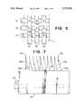
- FIG. 6shows the cross section of a graphite wafer with a knife edge.
- FIG. 7shows in cross section a prepared block of ten graphite wafers with a clamping fixture for sputtering carbon nano-cylinders.
- FIG. 8shows a diode for the power pulse technique with an inventively prepared field emission cathode.
- field emission cathodes of carbon nano-cylinderscan be produced, such as can be used, for example, as cathodes for diodes or switches.
- field emission cathodes for a field emitter arraycan be produced by the methods of microstructure technology.
- FIG. 6shows such a graphite wafer 100 with a knife edge 101, beveled on one side.
- FIG. 7shows how ten of these graphite wafers 100a to 100j are collected together into a block in a clamping fixture 103, in such a way that the knife edges 101a to 101j on one side of the block lie in one plane and an aluminum foil or Teflon foil is situated between each of the graphite wafers as a spacer 102a to 102j.
- the clamping fixtureconsists of two brass blocks, into which recesses have been milled to receive the ten graphite wafers with their spacer foils. These blocks are screwed together by two screws 104.
- the prepared blockis installed in a vacuum apparatus, in which a target of ultra-pure graphite is sputtered with an electron beam.
- the graphite target and the blockare arranged here in such a way that the carbon vapor strikes the plane of the graphite knife edges perpendicularly. Under these conditions, carbon nano-cylinders grow on the knife edges individually and in bundles of several cylinders, in the direction of the carbon vapor beam. When a layer several tenths of a micrometer thick has been reached, the sputtering process is terminated.
- the knife edges and the beveled surfaces of the graphite wafersare now coated with carbon nano-cylinders, which have extremely high mechanical strength.
- the microstructure of the surfaceis characterized by cylindrical elevations with sharp tips which have a radius of curvature of a few nanometers.
- FIG. 8shows how a graphite wafer prepared in this manner can be used in a diode that operates as a switching element.
- An anode 112 with a large surface and a cathode pin 111are fused in an evacuated glass flask 110.
- the graphite wafer 100 with its knife edge 101is fastened on the cathode pin in such a way that it is situated opposite the anode at a distance of about 1 mm. If a sufficiently high negative voltage is applied to the cathode, an electrical current can flow through the diode.
- knife edgesare characterized in that, in contrast to knife edges without carbon nano-cylinders, they amplify the electric field much more. A consequence of this is that, given the same voltage, the field emission current is much greater. Furthermore, the emission tips are not already destroyed after a brief operating time by the ions of the residual gas.
- the production method described abovecan easily be transferred to a rather large number of graphite wafers with longer knife edges. Also, the edge angle and the spacing between the knife edges can be varied within broad limits. This therefore represents a field emission cathode whose electron-emitting surface and current density can be adapted to many applications, for example in power pulse technology.
- FIG. 1shows a field emitter cathode with a gate electrode.
- Reference No. 10designates the electrically conducting, n-doped silicon substrate, 11 designates a sputtered insulating layer about 2 ⁇ m thick and consisting of SiO 2 .
- Reference No. 10designates the electrically conducting, n-doped silicon substrate, 11 designates a sputtered insulating layer about 2 ⁇ m thick and consisting of SiO 2 .
- the gate openings 14 of the molybdenum layerare preferably chosen to lie between 0.4 and 0.8 ⁇ m.
- a sacrificial layer of aluminumis applied to the field emitter array which, in this form, already corresponds to the prior art. This is done by rotating the substrate perpendicular to the surface and sputtering it with aluminum at slant incidence. This type of sputtering prevents the aluminum from depositing in the cathode openings.
- FIG. 2shows a field emitter element produced in accordance with this process step; the aluminum sacrificial layer is designated by 20.
- the graphite target disposed above the field emitter arrayis sputtered by an electron beam, and the carbon is deposited on the field emitter array.
- a portion of the carbon atomic beampenetrates through the gate opening and deposits on the cathode tips.
- cylindrical, parallel graphite fibersthus form in the direction of the incident atomic beam.
- the growth processis improved if, during this process step, a voltage U G of the order of 50 V is applied between the cathode and gate layer.
- FIG. 3shows a field emitter element made in accordance with this process step.
- 30designates the deposited carbon layer on the gate electrode
- 31designates one or more carbon nano-cylinders on the molybdenum tip.
- the voltage source to create the field strength at the cathode tipis also shown schematically.
- the growth of the carbon nano-cylinderscan be controlled through the emission current Ic.
- the processmust be terminated at the proper time, when the carbon nano-cylinders have reached a length of several tenths of a ⁇ m. It is here advantageous to modulate the gate voltage U G slightly.
- the quotient dIc/dU Gis designated as the differential slope and can be used as a measure of the quality of the field emitter array.
- the carbon layer with the aluminum sacrificial layeris etched off, so that, after this step, the field emitter element looks as shown in FIG. 4.
- the cathodesinstead of producing the cathodes so as to be electrically connected in their totality and lying at the same potential, they can also be produced in such a way that only one row of them is electrically coupled together.
- the gate electrodescan be produced in such a way that only one row of them is electrically coupled together, although perpendicular to the direction of the row of cathodes that are connected together. This then offers the possibility of driving each cathode individually.
- This type of circuitis already known and is used, for example, for a screen with digitally actuatable image points, from LETI Company (described in Busta loc. cit., pp. 69-70).
- This circuitfor the case of three rows of cathodes and three rows of gates, is shown schematically, in a top view, in FIG. 5.
- the gate electrodes G1, G2, and G3are applied in strips just like the cathodes, but perpendicular to the direction of the cathode tracks.
- the further process stepscorrespond to the steps used to produce the field emitter cathodes that cannot be individually actuated.
- the center electrode of the last column in FIG. 5can now be driven in such a way, for example, that a negative voltage is applied to the cathode strips K2 and a negative voltage is applied to the gate strips G3; a field emission current will then flow from this electrode, which can be measured in the cathode or gate circuit or which can be detected by a suction anode, which is not shown here.
- this arrangement of the cathode strips and gate stripscan be used to control specifically the production process of each individual cathode. It is then possible to measure the emission current from each field emitter tip during the production process, and not merely the total amount from the entire field emitter array. By turning off the voltage at one field emission cathode, one can favor the formation of an end cap with 5-ring structures, so that no further growth will occur.
- carbon nano-cylindersit is advantageous for the formation of carbon nano-cylinders to form them at elevated temperatures of 100° to 700° C. (degrees Celsius), preferably 300°-400° C.
- cathodes produced conventionally--by sputtering in vacuum by the methods of microstructure technology or by etchingare coated with electrically conducting host molecules.
- the host moleculescan be fullerenes, hetero-fullerenes, or their derivatives, especially also endohedral or exohedral compounds, for example of the type M 3 C 60 or M 3 C 70 , where M designates a metal, preferably the alkali metals potassium or sodium.
- the host moleculescan also be applied to the cathode in crystalline form, for example C 60 in the form of fullerite.
- the field emission cathodeswhose resistivity and emission properties have been improved by coating them with carbon nano-cylinders or also with fullerenes and their derivatives, in molecular or crystalline form, can be used wherever thermionic cathodes in vacuum were used previously, and in all applications of vacuum microelectronics. Typical fields of application will be listed below, without this listing being exhaustive, and a person skilled in the art can easily transfer the inventive field emission cathode to similar applications.
- Single emitter tips, emitter edges, or emitter arrayscan be used as electron sources for X-ray tubes, X-ray tubes with planar, drivable cathodes, for example for computer tomography, electron beam lithography, miniature electron microscopes, power switching tubes, diodes or triodes, logic circuit elements, video screens.
- Field emission cathodescan be used in miniaturized electronic components, such as ultra-high frequency diodes, ultra-high frequency triodes, diodes and triodes in combination with semiconductor components, temperature-stable diodes and triodes in the engines of motor vehicles, temperature-stable logic components, electronic components with diode and triode functions, which are particularly resistant to electromagnetic interference and ionizing radiation, pressure sensors, in which the cathode gate distance is influenced by the pressure, microwave generators and amplifiers.
- miniaturized electronic componentssuch as ultra-high frequency diodes, ultra-high frequency triodes, diodes and triodes in combination with semiconductor components, temperature-stable diodes and triodes in the engines of motor vehicles, temperature-stable logic components, electronic components with diode and triode functions, which are particularly resistant to electromagnetic interference and ionizing radiation, pressure sensors, in which the cathode gate distance is influenced by the pressure, microwave generators and amplifiers.
- field emission cathodescan be used preferably as electron sources with a large surface, yielding a high current density, drivable electron sources for planar video screens with a high light density in monochromatic or color designs.
Landscapes
- Cold Cathode And The Manufacture (AREA)
Abstract
Description
The invention relates to a field emission cathode device of an electrically conducting material and with a narrow, rod-shaped geometry or a knife edge to achieve high amplification of the electric field strength, such that the electron-emitting part of the field emission cathode has cylindrical molecules. The invention also relates to a method for producing such a field emission cathode device.
Field emission means the emission of electrons from the surface of an electric conductor under the action of an electric field exceeding 109 V/m. In practice, such field strengths are realized at sharp edges or tips, where the field strength is amplified. High vacuum is necessary to avoid gas discharges.
Field emission cathodes are used, for example, in field electron microscopes, in electron accelerators, in high-power switches (OS DE 39 24 745 A1) and in field emission diodes and field emitter arrays for vacuum microelectronics (thus for example Busta, Vacuum microelectronics--1992, Journal of Micromechanics and Microengineering, 2 (1992), pp. 53-60, and Iannazzo, A survey of the present status of vacuum microelectronics, Solid State Electronics, 36 (1993), pp. 301 to 320). A tungsten wire can be used as the field emission cathode, whose tip becomes so fine by etching that it can no longer be seen in an optical microscope. Also by etching, the ends of carbon fibers can be made sufficiently fine (Heinrich, Essig, Geiger, Appl. Phys. (1977) 12, pp. 197-202) to serve as a field emission cathode.
In vacuum microelectronics, field emission cathodes generally are produced by the methods of microprocess technology, by etching and sputtering, using lithographically produced masks (see Busta, Vacuum microelectronics--1992, Journal of Micromechanics and Microengineering, 2 (1992), pp. 53-60). By this method, one can produce conical tips with a radius of curvature of a few nm or wedge-shaped cutting edges with comparable radii of curvature. As materials for the cathode, one can use, for example, molybdenum, lanthanum hexaboride, hafnium, diamond-like carbon (B. C. Djubua, N. N. Chubun, Emission properties of Spindt-type cold cathodes with different emission cone material, IEEE Transactions on Electron Devices, 38 (1991) No. 10, pp. 2314-2316).
A disadvantage in the use of tips and edges, which have been produced by the known methods, is that the electron stream declines with operating time, since the tips or edges are destroyed by the positive ions of the unavoidable residual gas in the system. The like applies to field emission cathodes which are produced by sputtering techniques. The reason for this primarily is that the material structure of the emission tips is not uniquely defined. Thus, the geometry and microstructure of the tip and thus the work function of the electrons can vary within such wide limits that the electron streams from several tips, which were produced in one process, can differ by orders of magnitude, and furthermore change with operating time.
Furthermore, field emission cathodes for vacuum microelectronics cannot be produced in their optimal geometry by the prior art. Field strength calculations for various geometries of the tips show that the best shape of a field emission cathode is a narrow rod (Utsumi, Vacuum microelectronics: What's new and exciting, IEEE Transactions on Electron Devices 38 (1991), pp. 2276-2283). The present methods of microstructure technology can produce at most wedge-shaped tips in a defined manner.
Carbon nano-cylinders were observed for the first time in an electron microscope by Iijima (Nature, 354 (1991), p. 56). They can now be produced in large quantities, for example at the cathode of a visible arc (Iijima, Materials Science and Engineering, B19 (1993), pp. 172-180). In the presence of iron or cobalt, one can produce single-shell carbon nano-cylinders. Theoretical calculations show that, depending on the helicity of the hexagonal ring structure, the walls of the carbon nano-cylinders are electrically conducting or semiconducting (Saito, Fujita, Dresselhaus, Dresselhaus, Materials Science and Engineering, B19 (1993), pp. 185-191). The carbon nano-cylinders can also be filled with metals, for example with lead. Other methods for producing carbon nano-cylinders are described in the literature:
Carbon nano-cylinders can be produced by the catalytic decomposition of acetylene through iron particles at about 700° C. (Jose-Yacaman, Miki-Yoshida, Rendon, Applied Physics Letters 62 (6) 1993, pp. 657-659).
In the presence of methane, argon, and iron vapor, single-shell carbon nano-cylinders can be found in the carbon deposit on the chamber walls of a visible arc apparatus (Iijima, Nature 363 (1993), pp. 603-605).
By sputtering a carbon film in high vacuum, multiple-shell carbon nano-cylinders can be deposited on a graphite surface (Ge, Sattler, Science 260 (1993), pp. 515-518).
By sputtering ultra-pure graphite with electron beams in vacuum, carbon nano-cylinders can be produced on substrates consisting of various materials, such that the carbon nano-cylinders are aligned in the direction of the vapor jet (Kosakovskaya et al., JETP Lett., 56 (1992), p. 26).
In addition to the carbon nano-cylinders, disordered carbon particles generally are also deposited on the substrate. These can be removed, for example, by treatment in an oxidizing atmosphere at an elevated temperature up to 500° C., preferably 400° C. The carbon nano-cylinders at the end caps can be opened in a similar manner in an oxidizing atmosphere (air, CO2, or pure oxygen). This offers the possibility of filling the carbon nano-cylinders with metals, as described for a filling with lead by Ajayan and Iijima in Nature 361, p. 333.
In principle, it is possible to fasten these carbon nano-cylinders, produced by one of the above methods, on a suitable substrate, by means of micro-manipulators, and thus to produce a field emission cathode. However, this method is impractical, and in particular is not suited for field electron arrays with many cathode tips, as is desired in vacuum microelectronics.
Field emission cathodes with emission tips of bio-molecular microstructures or a metal-semiconductor-eutectic are known from the U.S. Pat No. 5,138,220. The diameter of these structures measures in the micrometer range, and subsequent metallization is necessary to achieve adequate emission.
The publication IBM Technical Disclosure Bulletin, Vol. 35, No. 7, December 1992, pp. 410-411 describes the use of Buckminster fullerene molecules as the tip of scanning-probe microscopes. Besides spherical C60 molecules, derivatives of C60 - and hetero-fullerenes are mentioned, that is host molecules in which individual C-atoms have been substituted by boron or nitrogen.
The present invention is based on the object or on the technical problem of specifying a field emission cathode which avoids the disadvantages of the prior art, assures high emission quality, makes possible a longer lifetime, and in particular resists bombardment with residual gas ions. Furthermore, the present invention is based on the object or on the technical problem of specifying a method for producing a field emission cathode of the type mentioned in the introduction, so as to assure technically optimal manufacture together with economy.
The inventive field emission cathode device consists of an electrically conducting material and having the shape of a narrow rod or a knife edge to achieve high magnification of the electric field strength, such that the electron emitting part of the field emission cathode has cylindrical molecules, wherein the cylindrical molecules are formed at least in part as single-shell or multiple-shell carbon nano-cylinders. The inventive method for producing the field emission cathode device with carbon non-cylinders which have been expanded during the gas phase. Advantageous modifications and developments are the subject of the subclaims.
An especially preferred design of the inventive field emission cathode is characterized in that carbon nano-cylinders are used as field emission cathodes. Single-shell carbon nano-cylinders with a diameter of about 1 nanometer and a length greater than 1 micrometer, or also multiple-shell ones with a diameter up to several nanometers can be produced. Bundles of single-shell carbon nano-cylinders with diameters of about 5 nanometers can also be produced. The walls of the carbon nano-cylinders consist of carbon atoms in a hexagonal pattern, while the end caps additionally contain 5-ring structures. The individual carbon atoms of the carbon nano-cylinders are strongly bound chemically, as a result of which the carbon nano-cylinders have extremely great mechanical strength. This also results in their high sputtering strength in comparison to randomly grown tips, which are sputtered according to the prior art.
Using well-known carbon nano-cylinders as a field emission cathode thus combines the advantage of optimal geometry with high strength, thus assuring that the emission properties of such field emission cathodes will not change during their operation, in contrast to previously used cathode tips.
So that the above advantages of the carbon nano-cylinders can also be used for making the field emission cathode arrays of vacuum microelectronics, the known methods for producing such arrays must be modified according to the invention, in such a way that the carbon nano-cylinders grow on appropriately prepared locations of a substrate.
The production method can be used to produce either individual field emission cathodes or also field emission cathode arrays.
Further embodiments and advantages of the invention derive from the other characteristics cited in the claims, and from the embodiments given below. The characteristics of the inventions can be combined with one another in arbitrary fashion, unless they obviously exclude one another.
The invention as well as advantageous embodiments and developments thereof are described and elucidated in more detail below in terms of the examples shown in the drawings. The features contained in the description and in the drawings can be used inventively individually by themselves or in various combinations.
FIG. 1 shows an individual field emission element of a field emitter array, such as can be produced by the prior art.
FIG. 2 shows the same element in accordance with the first inventive process step, so as to provide the emission tip with carbon nano-cylinders.
FIG. 3 shows the same element after carbon has been sputtered.
FIG. 4 shows the same element after the last process step, in its final state.
FIG. 5 shows a section of a field emitter array with individually actuatable emission tips.
FIG. 6 shows the cross section of a graphite wafer with a knife edge.
FIG. 7 shows in cross section a prepared block of ten graphite wafers with a clamping fixture for sputtering carbon nano-cylinders.
FIG. 8 shows a diode for the power pulse technique with an inventively prepared field emission cathode.
Below it will be explained, by way of an example, how field emission cathodes of carbon nano-cylinders can be produced, such as can be used, for example, as cathodes for diodes or switches. By way of a second example, it will be explained how field emission cathodes for a field emitter array can be produced by the methods of microstructure technology.
Example: Production of individual cathodes on a knife edge
Square graphite wafers about 1 cm (centimeter) on a side, and 1 mm (millimeter) thick are ground or etched to a knife edge on one side. FIG. 6 shows such agraphite wafer 100 with aknife edge 101, beveled on one side. FIG. 7 shows how ten of these graphite wafers 100a to 100j are collected together into a block in aclamping fixture 103, in such a way that the knife edges 101a to 101j on one side of the block lie in one plane and an aluminum foil or Teflon foil is situated between each of the graphite wafers as aspacer 102a to 102j. The clamping fixture consists of two brass blocks, into which recesses have been milled to receive the ten graphite wafers with their spacer foils. These blocks are screwed together by twoscrews 104.
The prepared block is installed in a vacuum apparatus, in which a target of ultra-pure graphite is sputtered with an electron beam. The graphite target and the block are arranged here in such a way that the carbon vapor strikes the plane of the graphite knife edges perpendicularly. Under these conditions, carbon nano-cylinders grow on the knife edges individually and in bundles of several cylinders, in the direction of the carbon vapor beam. When a layer several tenths of a micrometer thick has been reached, the sputtering process is terminated.
The knife edges and the beveled surfaces of the graphite wafers are now coated with carbon nano-cylinders, which have extremely high mechanical strength. The microstructure of the surface is characterized by cylindrical elevations with sharp tips which have a radius of curvature of a few nanometers.
FIG. 8 shows how a graphite wafer prepared in this manner can be used in a diode that operates as a switching element. Ananode 112 with a large surface and a cathode pin 111 are fused in an evacuatedglass flask 110. Thegraphite wafer 100 with itsknife edge 101 is fastened on the cathode pin in such a way that it is situated opposite the anode at a distance of about 1 mm. If a sufficiently high negative voltage is applied to the cathode, an electrical current can flow through the diode.
In the same manner, several knife edges instead of a single knife edge can be used as a cathode.
These knife edges are characterized in that, in contrast to knife edges without carbon nano-cylinders, they amplify the electric field much more. A consequence of this is that, given the same voltage, the field emission current is much greater. Furthermore, the emission tips are not already destroyed after a brief operating time by the ions of the residual gas.
The production method described above can easily be transferred to a rather large number of graphite wafers with longer knife edges. Also, the edge angle and the spacing between the knife edges can be varied within broad limits. This therefore represents a field emission cathode whose electron-emitting surface and current density can be adapted to many applications, for example in power pulse technology.
Example: Production of field emission cathodes as an array
First, an array of field emitter cathodes and gate electrodes of molybdenum will be produced on a doped silicon substrate, in accordance with a previously known method, and specifically by the methods of silicon processing technology, as is described, for example, in the article, Spindt et al., J. Appl. Physics 47 (1976), p. 5248ff (see also Busta loc. cit. and Iannazzo loc. cit.). FIG. 1 shows a field emitter cathode with a gate electrode. Reference No. 10 designates the electrically conducting, n-doped silicon substrate, 11 designates a sputtered insulating layer about 2 μm thick and consisting of SiO2. Reference No. 12 designates the sputtered molybdenum gate electrode, about 0.5 μm thick. Reference No. 13 designates the tip-shaped field emission cathode of molybdenum. Thegate openings 14 of the molybdenum layer are preferably chosen to lie between 0.4 and 0.8 μm. By means of the above-cited production method, one thus achieves the result that the cathode cone tips lie about 0.5 μm below the gate electrodes.
In a following process step, a sacrificial layer of aluminum is applied to the field emitter array which, in this form, already corresponds to the prior art. This is done by rotating the substrate perpendicular to the surface and sputtering it with aluminum at slant incidence. This type of sputtering prevents the aluminum from depositing in the cathode openings. FIG. 2 shows a field emitter element produced in accordance with this process step; the aluminum sacrificial layer is designated by 20.
In a subsequent process step, the graphite target disposed above the field emitter array is sputtered by an electron beam, and the carbon is deposited on the field emitter array. A portion of the carbon atomic beam penetrates through the gate opening and deposits on the cathode tips. As is known from a publication by Kosakovskaya et al., JETP Lett., 56 (1992) 26, cylindrical, parallel graphite fibers thus form in the direction of the incident atomic beam. The growth process is improved if, during this process step, a voltage UG of the order of 50 V is applied between the cathode and gate layer. The average field strength is then of the order of 50 V/0.5 μm=108 V/m; because the field strength is amplified at the tip, it there rises to over about 109 V/m. The high field strength at the fiber tip evidently causes the fiber ends to remain open and improves the growth of the fibers (Smalley, loc. cit. p. 4). FIG. 3 shows a field emitter element made in accordance with this process step. Here, 30 designates the deposited carbon layer on the gate electrode, and 31 designates one or more carbon nano-cylinders on the molybdenum tip. The voltage source to create the field strength at the cathode tip is also shown schematically.
The growth of the carbon nano-cylinders can be controlled through the emission current Ic. The longer the grown carbon nano-cylinders, the stronger becomes the emission current. The process must be terminated at the proper time, when the carbon nano-cylinders have reached a length of several tenths of a μm. It is here advantageous to modulate the gate voltage UG slightly. The quotient dIc/dUG is designated as the differential slope and can be used as a measure of the quality of the field emitter array.
In a last step, the carbon layer with the aluminum sacrificial layer is etched off, so that, after this step, the field emitter element looks as shown in FIG. 4.
In a modification of the production process described above, instead of producing the cathodes so as to be electrically connected in their totality and lying at the same potential, they can also be produced in such a way that only one row of them is electrically coupled together. In the same manner, the gate electrodes can be produced in such a way that only one row of them is electrically coupled together, although perpendicular to the direction of the row of cathodes that are connected together. This then offers the possibility of driving each cathode individually. This type of circuit is already known and is used, for example, for a screen with digitally actuatable image points, from LETI Company (described in Busta loc. cit., pp. 69-70). This circuit, for the case of three rows of cathodes and three rows of gates, is shown schematically, in a top view, in FIG. 5. Electrically conducting cathode tracks K1, K2, and K3, for example consisting of n-doped silicon, are applied on a substrate with an electrically non-conducting surface 1, along a width of a few micrometers. The following insulating layer of silicon dioxide (not shown), about 2 micrometers thick, corresponds to the arrangement described by Spindt. The gate electrodes G1, G2, and G3 are applied in strips just like the cathodes, but perpendicular to the direction of the cathode tracks. The further process steps correspond to the steps used to produce the field emitter cathodes that cannot be individually actuated.
The center electrode of the last column in FIG. 5 can now be driven in such a way, for example, that a negative voltage is applied to the cathode strips K2 and a negative voltage is applied to the gate strips G3; a field emission current will then flow from this electrode, which can be measured in the cathode or gate circuit or which can be detected by a suction anode, which is not shown here.
In the production method described here, this arrangement of the cathode strips and gate strips can be used to control specifically the production process of each individual cathode. It is then possible to measure the emission current from each field emitter tip during the production process, and not merely the total amount from the entire field emitter array. By turning off the voltage at one field emission cathode, one can favor the formation of an end cap with 5-ring structures, so that no further growth will occur.
It is advantageous for the formation of carbon nano-cylinders to form them at elevated temperatures of 100° to 700° C. (degrees Celsius), preferably 300°-400° C.
It is also advantageous to apply a layer of iron or cobalt, a few atomic layers thick, on the molybdenum cathode tips before sputtering on the carbon. The iron and cobalt evidently have a positive catalytic effect on the formation of carbon nano-cylinders.
As a modification of the invention, one can also dispense with the advantage of the narrow, cylindrical shape of the carbon nano-cylinders and utilize only the advantage of the high mechanical stability of host molecules, that is their resistance to the bombardment of the cathode by positive residual gas ions. In this case, cathodes produced conventionally--by sputtering in vacuum by the methods of microstructure technology or by etching, are coated with electrically conducting host molecules. The host molecules can be fullerenes, hetero-fullerenes, or their derivatives, especially also endohedral or exohedral compounds, for example of the type M3 C60 or M3 C70, where M designates a metal, preferably the alkali metals potassium or sodium. The host molecules can also be applied to the cathode in crystalline form, for example C60 in the form of fullerite.
The field emission cathodes, whose resistivity and emission properties have been improved by coating them with carbon nano-cylinders or also with fullerenes and their derivatives, in molecular or crystalline form, can be used wherever thermionic cathodes in vacuum were used previously, and in all applications of vacuum microelectronics. Typical fields of application will be listed below, without this listing being exhaustive, and a person skilled in the art can easily transfer the inventive field emission cathode to similar applications.
Single emitter tips, emitter edges, or emitter arrays can be used as electron sources for X-ray tubes, X-ray tubes with planar, drivable cathodes, for example for computer tomography, electron beam lithography, miniature electron microscopes, power switching tubes, diodes or triodes, logic circuit elements, video screens.
Field emission cathodes can be used in miniaturized electronic components, such as ultra-high frequency diodes, ultra-high frequency triodes, diodes and triodes in combination with semiconductor components, temperature-stable diodes and triodes in the engines of motor vehicles, temperature-stable logic components, electronic components with diode and triode functions, which are particularly resistant to electromagnetic interference and ionizing radiation, pressure sensors, in which the cathode gate distance is influenced by the pressure, microwave generators and amplifiers.
As arrays, field emission cathodes can be used preferably as electron sources with a large surface, yielding a high current density, drivable electron sources for planar video screens with a high light density in monochromatic or color designs.
Claims (9)
1. A field emission cathode which consists of an electrically conducting material having the shape of a narrow rod or a knife edge to achieve high magnification of the electric field strength, such that the electron-emitting part of the field emission cathode has cylindrical molecules formed at least in part as single-shell or multiple-shell carbon nano-cylinders.
2. The device of claim 1, wherein the carbon nano-cylinders have end caps.
3. The device of claim 1, wherein the single- or multiple-shell carbon nano-cylinders are collected into bundles.
4. The device of claim 1, wherein the carbon nano-cylinders are filled with metal.
5. The device of claim 1, wherein the carbon nano-cylinders at least partly have endohedral or exohedral compounds with other atoms or molecules.
6. The device of claim 1, wherein the field emission cathode forms the tip of a field electron microscope, a field ion microscope, a scanning tunnel microscope, or a scanning power microscope.
7. The device of claim 1, wherein a plurality of similar field emission cathodes is disposed in a line or a plane, and thereby forms a linear or planar electron source.
8. The device of claim 1, wherein a plurality of similar field emission cathodes is disposed in a plane in the form of a matrix, and the field emission cathodes can be driven individually, and the field emission cathodes represent the electron sources for the image points of a visual display system.
9. The device of claim 8, wherein the plurality of similar field emission cathodes is in the range of 10,000 to 100,000 molecules.
Priority Applications (3)
| Application Number | Priority Date | Filing Date | Title |
|---|---|---|---|
| US10/408,871USRE38561E1 (en) | 1995-02-22 | 1995-02-22 | Field emission cathode |
| US09/504,635USRE38223E1 (en) | 1994-02-23 | 1995-02-22 | Field emission cathode having an electrically conducting material shaped of a narrow rod or knife edge |
| US10/409,363US20040036402A1 (en) | 1994-02-23 | 2003-04-08 | Field emission cathode using carbon fibers |
Applications Claiming Priority (3)
| Application Number | Priority Date | Filing Date | Title |
|---|---|---|---|
| DE4405768.7 | 1994-02-23 | ||
| DE4405768ADE4405768A1 (en) | 1994-02-23 | 1994-02-23 | Field emission cathode device and method for its manufacture |
| PCT/DE1995/000221WO1995023424A1 (en) | 1994-02-23 | 1995-02-22 | Field-emission cathode and method of manufacturing it |
Related Parent Applications (2)
| Application Number | Title | Priority Date | Filing Date |
|---|---|---|---|
| PCT/DE1995/000221A-371-Of-InternationalWO1995023424A1 (en) | 1994-02-23 | 1995-02-22 | Field-emission cathode and method of manufacturing it |
| US09/504,635ContinuationUSRE38223E1 (en) | 1994-02-23 | 1995-02-22 | Field emission cathode having an electrically conducting material shaped of a narrow rod or knife edge |
Related Child Applications (2)
| Application Number | Title | Priority Date | Filing Date |
|---|---|---|---|
| US10/408,871ReissueUSRE38561E1 (en) | 1995-02-22 | 1995-02-22 | Field emission cathode |
| US09/504,635ReissueUSRE38223E1 (en) | 1994-02-23 | 1995-02-22 | Field emission cathode having an electrically conducting material shaped of a narrow rod or knife edge |
Publications (1)
| Publication Number | Publication Date |
|---|---|
| US5773921Atrue US5773921A (en) | 1998-06-30 |
Family
ID=6510961
Family Applications (3)
| Application Number | Title | Priority Date | Filing Date |
|---|---|---|---|
| US08/702,684CeasedUS5773921A (en) | 1994-02-23 | 1995-02-22 | Field emission cathode having an electrically conducting material shaped of a narrow rod or knife edge |
| US09/504,635Expired - LifetimeUSRE38223E1 (en) | 1994-02-23 | 1995-02-22 | Field emission cathode having an electrically conducting material shaped of a narrow rod or knife edge |
| US10/409,363AbandonedUS20040036402A1 (en) | 1994-02-23 | 2003-04-08 | Field emission cathode using carbon fibers |
Family Applications After (2)
| Application Number | Title | Priority Date | Filing Date |
|---|---|---|---|
| US09/504,635Expired - LifetimeUSRE38223E1 (en) | 1994-02-23 | 1995-02-22 | Field emission cathode having an electrically conducting material shaped of a narrow rod or knife edge |
| US10/409,363AbandonedUS20040036402A1 (en) | 1994-02-23 | 2003-04-08 | Field emission cathode using carbon fibers |
Country Status (5)
| Country | Link |
|---|---|
| US (3) | US5773921A (en) |
| EP (1) | EP0801805B1 (en) |
| AT (1) | ATE186422T1 (en) |
| DE (2) | DE4405768A1 (en) |
| WO (1) | WO1995023424A1 (en) |
Cited By (117)
| Publication number | Priority date | Publication date | Assignee | Title |
|---|---|---|---|---|
| US5973444A (en)* | 1995-12-20 | 1999-10-26 | Advanced Technology Materials, Inc. | Carbon fiber-based field emission devices |
| WO2000019494A1 (en)* | 1998-09-28 | 2000-04-06 | Xidex Corporation | Method for manufacturing carbon nanotubes as functional elements of mems devices |
| WO2000030141A1 (en)* | 1998-11-12 | 2000-05-25 | The Board Of Trustees Of The Leland Stanford Junior University | Self-oriented bundles of carbon nanotubes and method of making same |
| EP1022763A1 (en)* | 1999-01-25 | 2000-07-26 | Lucent Technologies Inc. | Article comprising aligned, truncated carbon nanotubes and process for fabricating article |
| EP1022764A1 (en)* | 1999-01-25 | 2000-07-26 | Lucent Technologies Inc. | Article comprising enhanced nanotube emitter structure and process for fabricating article |
| US6097138A (en)* | 1996-09-18 | 2000-08-01 | Kabushiki Kaisha Toshiba | Field emission cold-cathode device |
| US6146227A (en)* | 1998-09-28 | 2000-11-14 | Xidex Corporation | Method for manufacturing carbon nanotubes as functional elements of MEMS devices |
| EP1061555A1 (en)* | 1999-06-18 | 2000-12-20 | Iljin Nanotech Co., Ltd. | White light source using carbon nanotubes and fabrication method thereof |
| EP1061554A1 (en)* | 1999-06-15 | 2000-12-20 | Iljin Nanotech Co., Ltd. | White light source using carbon nanotubes and fabrication method thereof |
| EP1061544A1 (en)* | 1999-06-15 | 2000-12-20 | Iljin Nanotech Co., Ltd. | Field emitter having carbon nanotube film, method of fabricating the same, and field emission display device using the field emitter. |
| US6277318B1 (en)* | 1999-08-18 | 2001-08-21 | Agere Systems Guardian Corp. | Method for fabrication of patterned carbon nanotube films |
| US20010040215A1 (en)* | 2000-03-16 | 2001-11-15 | Haroon Ahmed | Apparatus for producing a flux of charge carriers |
| US20020057045A1 (en)* | 2000-09-01 | 2002-05-16 | Takeo Tsukamoto | Electron-emitting device, electron source and image-forming apparatus, and method for manufacturing electron emitting device |
| US20020060516A1 (en)* | 2000-09-01 | 2002-05-23 | Shinichi Kawate | Electron-emitting devices, electron sources, and image-forming apparatus |
| US6401526B1 (en) | 1999-12-10 | 2002-06-11 | The Board Of Trustees Of The Leland Stanford Junior University | Carbon nanotubes and methods of fabrication thereof using a liquid phase catalyst precursor |
| WO2001084130A3 (en)* | 2000-05-01 | 2002-06-13 | El Mul Technologies Ltd | A nanotube-based electron emission device and systems using the same |
| US20020074947A1 (en)* | 2000-09-01 | 2002-06-20 | Takeo Tsukamoto | Electron-emitting device, electron-emitting apparatus, image display apparatus, and light-emitting apparatus |
| US20020094064A1 (en)* | 2000-10-06 | 2002-07-18 | Zhou Otto Z. | Large-area individually addressable multi-beam x-ray system and method of forming same |
| US20020110996A1 (en)* | 2000-12-08 | 2002-08-15 | Si Diamond Technology, Inc. | Low work function material |
| US6440761B1 (en)* | 1999-05-24 | 2002-08-27 | Samsung Sdi Co., Ltd. | Carbon nanotube field emission array and method for fabricating the same |
| US6445006B1 (en) | 1995-12-20 | 2002-09-03 | Advanced Technology Materials, Inc. | Microelectronic and microelectromechanical devices comprising carbon nanotube components, and methods of making same |
| US6456691B2 (en)* | 2000-03-06 | 2002-09-24 | Rigaku Corporation | X-ray generator |
| EP1251543A1 (en)* | 2001-04-18 | 2002-10-23 | VA TECH Transmission & Distribution GmbH & Co. KEG | Vacuum power switches |
| US20020167256A1 (en)* | 1997-10-30 | 2002-11-14 | Tatsuya Iwasaki | Structure and a process for its production |
| US20020185949A1 (en)* | 2001-06-07 | 2002-12-12 | Si Diamond Technology, Inc. | Field emission display using carbon nanotubes and methods of making the same |
| US20020185950A1 (en)* | 2001-06-08 | 2002-12-12 | Sony Corporation And Sony Electronics Inc. | Carbon cathode of a field emission display with in-laid isolation barrier and support |
| US20020185951A1 (en)* | 2001-06-08 | 2002-12-12 | Sony Corporation | Carbon cathode of a field emission display with integrated isolation barrier and support on substrate |
| EP1271594A1 (en)* | 2001-06-29 | 2003-01-02 | Canon Kabushiki Kaisha | Electron-emitting device, electron source, and image-forming apparatus |
| US6504292B1 (en) | 1999-07-15 | 2003-01-07 | Agere Systems Inc. | Field emitting device comprising metallized nanostructures and method for making the same |
| US20030006684A1 (en)* | 2001-03-27 | 2003-01-09 | Shinichi Kawate | Catalyst used to form carbon fiber, method of making the same and electron emitting device, electron source, image forming apparatus, secondary battery and body for storing hydrogen |
| US20030039750A1 (en)* | 2001-08-24 | 2003-02-27 | Dongsheng Mao | Catalyst for carbon nanotube growth |
| US20030042834A1 (en)* | 2001-08-29 | 2003-03-06 | Motorola, Inc. | Field emission display and methods of forming a field emission display |
| US20030042833A1 (en)* | 2001-08-28 | 2003-03-06 | Motorola, Inc. | Method for activating nanotubes as field emission sources |
| US6531828B2 (en)* | 1999-07-19 | 2003-03-11 | Zvi Yaniv | Alignment of carbon nanotubes |
| US20030048055A1 (en)* | 2001-09-10 | 2003-03-13 | Junri Ishikura | Manufacture method for electron-emitting device, electron source, light-emitting apparatus, and image forming apparatus |
| US6538367B1 (en) | 1999-07-15 | 2003-03-25 | Agere Systems Inc. | Field emitting device comprising field-concentrating nanoconductor assembly and method for making the same |
| US20030057860A1 (en)* | 2001-09-07 | 2003-03-27 | Takeo Tsukamoto | Electron-emitting device, electron source, image forming apparatus, and method of manufacturing electron-emitting device and electron source |
| US6545396B1 (en)* | 1999-10-21 | 2003-04-08 | Sharp Kabushiki Kaisha | Image forming device using field emission electron source arrays |
| US6553096B1 (en) | 2000-10-06 | 2003-04-22 | The University Of North Carolina Chapel Hill | X-ray generating mechanism using electron field emission cathode |
| US20030111946A1 (en)* | 2001-12-18 | 2003-06-19 | Talin Albert Alec | FED cathode structure using electrophoretic deposition and method of fabrication |
| US6586889B1 (en) | 2000-06-21 | 2003-07-01 | Si Diamond Technology, Inc. | MEMS field emission device |
| US6597090B1 (en) | 1998-09-28 | 2003-07-22 | Xidex Corporation | Method for manufacturing carbon nanotubes as functional elements of MEMS devices |
| WO2003060923A1 (en) | 2002-01-15 | 2003-07-24 | International Business Machines Corporation | Microstructures |
| JP3441396B2 (en) | 1998-12-03 | 2003-09-02 | 喜萬 中山 | Probe for surface signal operation of electronic device and method of manufacturing the same |
| JP3441397B2 (en) | 1998-12-31 | 2003-09-02 | 喜萬 中山 | Fusion probe for surface signal operation of electronic device and method of manufacturing the same |
| US6624589B2 (en) | 2000-05-30 | 2003-09-23 | Canon Kabushiki Kaisha | Electron emitting device, electron source, and image forming apparatus |
| US6628053B1 (en) | 1997-10-30 | 2003-09-30 | Canon Kabushiki Kaisha | Carbon nanotube device, manufacturing method of carbon nanotube device, and electron emitting device |
| US6630772B1 (en) | 1998-09-21 | 2003-10-07 | Agere Systems Inc. | Device comprising carbon nanotube field emitter structure and process for forming device |
| US20030193297A1 (en)* | 2002-04-16 | 2003-10-16 | Sony Corporation | Field emission cathode structure using perforated gate |
| US20030193296A1 (en)* | 2002-04-16 | 2003-10-16 | Sony Corporation | Field emission display using line cathode structure |
| US6649431B2 (en)* | 2001-02-27 | 2003-11-18 | Ut. Battelle, Llc | Carbon tips with expanded bases grown with simultaneous application of carbon source and etchant gases |
| US6664728B2 (en) | 2000-09-22 | 2003-12-16 | Nano-Proprietary, Inc. | Carbon nanotubes with nitrogen content |
| US20040007955A1 (en)* | 2002-07-09 | 2004-01-15 | Zvi Yaniv | Nanotriode utilizing carbon nanotubes and fibers |
| US20040007988A1 (en)* | 2002-04-16 | 2004-01-15 | Sony Corporation, A Japanese Corporation | Field emission display with deflecting MEMS electrodes |
| US20040028183A1 (en)* | 2000-10-06 | 2004-02-12 | Jianping Lu | Method and apparatus for controlling electron beam current |
| US6692324B2 (en)* | 2000-08-29 | 2004-02-17 | Ut-Battelle, Llc | Single self-aligned carbon containing tips |
| US20040036403A1 (en)* | 2000-12-13 | 2004-02-26 | Takahito Ono | Fabrication method of carbon nanotubes |
| US6700454B2 (en) | 2001-06-29 | 2004-03-02 | Zvi Yaniv | Integrated RF array using carbon nanotube cathodes |
| US20040070326A1 (en)* | 2002-10-09 | 2004-04-15 | Nano-Proprietary, Inc. | Enhanced field emission from carbon nanotubes mixed with particles |
| US20040090163A1 (en)* | 2001-06-08 | 2004-05-13 | Sony Corporation | Field emission display utilizing a cathode frame-type gate |
| US20040100184A1 (en)* | 2002-11-27 | 2004-05-27 | Sony Corporation | Spacer-less field emission display |
| US20040104667A1 (en)* | 2001-06-08 | 2004-06-03 | Sony Corporation | Field emission display using gate wires |
| US20040114721A1 (en)* | 2000-10-06 | 2004-06-17 | Applied Nanotechnologies, Inc. | Devices and methods for producing multiple x-ray beams from multiple locations |
| US6764874B1 (en) | 2003-01-30 | 2004-07-20 | Motorola, Inc. | Method for chemical vapor deposition of single walled carbon nanotubes |
| US20040145299A1 (en)* | 2003-01-24 | 2004-07-29 | Sony Corporation | Line patterned gate structure for a field emission display |
| US20040160157A1 (en)* | 2003-02-19 | 2004-08-19 | Futaba Corporation | Carbon substance and method for manufacturing the same, electron emission element and composite materials |
| US6783589B2 (en) | 2001-01-19 | 2004-08-31 | Chevron U.S.A. Inc. | Diamondoid-containing materials in microelectronics |
| US20040183757A1 (en)* | 2003-01-28 | 2004-09-23 | Canon Kabushiki Kaisha | Driving method for electron-emitting device, driving method for electron source, manufacturing method for electron source, and image display apparatus |
| US20040189554A1 (en)* | 2003-03-31 | 2004-09-30 | Sony Corporation | Image display device incorporating driver circuits on active substrate and other methods to reduce interconnects |
| US20040189552A1 (en)* | 2003-03-31 | 2004-09-30 | Sony Corporation | Image display device incorporating driver circuits on active substrate to reduce interconnects |
| US20040192997A1 (en)* | 2003-03-26 | 2004-09-30 | Lovoi Paul A. | Miniature x-ray tube with micro cathode |
| US6819034B1 (en) | 2000-08-21 | 2004-11-16 | Si Diamond Technology, Inc. | Carbon flake cold cathode |
| US20040245911A1 (en)* | 2003-06-06 | 2004-12-09 | Electrovac Fabrikation Elektrotechnischer Spezialartikel Gmbh | Electron emitter and process of fabrication |
| US20040245910A1 (en)* | 2003-06-06 | 2004-12-09 | Electrovac Fabrikation Elektrotechnischer Spezialartikel Gmbh | Field emission backlight for liquid crystal televisions |
| US20040245224A1 (en)* | 2003-05-09 | 2004-12-09 | Nano-Proprietary, Inc. | Nanospot welder and method |
| US20040251478A1 (en)* | 2001-01-19 | 2004-12-16 | Chevron U.S.A. Inc. | Diamondoid-containing materials for passivating layers in integrated circuit devices |
| US6836066B1 (en)* | 2000-02-25 | 2004-12-28 | Samsung Sdi Co., Ltd. | Triode field emission display using carbon nanobtubes |
| US20050019576A1 (en)* | 2001-01-19 | 2005-01-27 | Chevron U.S.A. Inc. | Nucleation of diamond films using higher diamondoids |
| US6848962B2 (en) | 2000-09-01 | 2005-02-01 | Canon Kabushiki Kaisha | Electron-emitting device, electron source, image-forming apparatus, and method for producing electron-emitting device and electron-emitting apparatus |
| US6853126B2 (en) | 2000-09-22 | 2005-02-08 | Canon Kabushiki Kaisha | Electron-emitting device, electron source, image forming apparatus, and electron-emitting apparatus |
| WO2004088701A3 (en)* | 2003-03-26 | 2005-04-14 | Xoft Microtube Inc | Miniature x-ray tube with micro cathode |
| US20050090176A1 (en)* | 2001-08-29 | 2005-04-28 | Dean Kenneth A. | Field emission display and methods of forming a field emission display |
| US20050140261A1 (en)* | 2003-10-23 | 2005-06-30 | Pinchas Gilad | Well structure with axially aligned field emission fiber or carbon nanotube and method for making same |
| US20050168122A1 (en)* | 2004-02-04 | 2005-08-04 | Chevron U.S.A. Inc. | Heterodiamondoid-containing field emission devices |
| US20050200261A1 (en)* | 2000-12-08 | 2005-09-15 | Nano-Proprietary, Inc. | Low work function cathode |
| US20050226361A1 (en)* | 2000-10-06 | 2005-10-13 | The University Of North Carolina At Chapel Hill | Computed tomography scanning system and method using a field emission x-ray source |
| US6958475B1 (en) | 2003-01-09 | 2005-10-25 | Colby Steven M | Electron source |
| US20060008047A1 (en)* | 2000-10-06 | 2006-01-12 | The University Of North Carolina At Chapel Hill | Computed tomography system for imaging of human and small animal |
| US20060177602A1 (en)* | 2004-07-07 | 2006-08-10 | Commissariat A L'energie Atomique | Low temperature growth of oriented carbon nanotubes |
| US20060226550A1 (en)* | 2002-03-20 | 2006-10-12 | Board To Trustees Of The Leland Stanford Junior University | Molybdenum-based electrode with carbon nanotube growth |
| US20070053489A1 (en)* | 2005-04-25 | 2007-03-08 | The University Of North Carolina At Chapel Hill | X-ray imaging systems and methods using temporal digital signal processing for reducing noise and for obtaining multiple images simultaneously |
| US20070158768A1 (en)* | 2006-01-06 | 2007-07-12 | Honeywell International, Inc. | Electrical contacts formed of carbon nanotubes |
| US20080012461A1 (en)* | 2004-11-09 | 2008-01-17 | Nano-Proprietary, Inc. | Carbon nanotube cold cathode |
| US20080069420A1 (en)* | 2006-05-19 | 2008-03-20 | Jian Zhang | Methods, systems, and computer porgram products for binary multiplexing x-ray radiography |
| WO2008054451A3 (en)* | 2006-02-06 | 2008-07-17 | Univ North Carolina | Synthesis and processing of rare-earth boride nanowires as electron emitters |
| US20080220181A1 (en)* | 2006-08-25 | 2008-09-11 | Philadelphia Health & Education Corporation, D/B/A Drexel University College Of Medicine | Method of loading a nanotube structure and loaded nanotube structure |
| US20090022264A1 (en)* | 2007-07-19 | 2009-01-22 | Zhou Otto Z | Stationary x-ray digital breast tomosynthesis systems and related methods |
| US20100078557A1 (en)* | 2008-09-30 | 2010-04-01 | Carl Zeiss Nts Gmbh | Electron beam source and method of manufacturing the same |
| CN1833299B (en)* | 2003-05-30 | 2010-06-16 | 新泰科有限公司 | Devices and methods for producing multiple x-ray beams from multiple locations |
| US20100239064A1 (en)* | 2005-04-25 | 2010-09-23 | Unc-Chapel Hill | Methods, systems, and computer program products for multiplexing computed tomography |
| FR2946456A1 (en)* | 2009-06-05 | 2010-12-10 | Thales Sa | COLLIMATE ELECTRONIC BEAM SOURCE WITH COLD CATHODE |
| US20100329413A1 (en)* | 2009-01-16 | 2010-12-30 | Zhou Otto Z | Compact microbeam radiation therapy systems and methods for cancer treatment and research |
| US8358739B2 (en) | 2010-09-03 | 2013-01-22 | The University Of North Carolina At Chapel Hill | Systems and methods for temporal multiplexing X-ray imaging |
| US8536773B2 (en) | 2011-03-30 | 2013-09-17 | Carl Zeiss Microscopy Gmbh | Electron beam source and method of manufacturing the same |
| US20140183349A1 (en)* | 2012-12-27 | 2014-07-03 | Schlumberger Technology Corporation | Ion source using spindt cathode and electromagnetic confinement |
| US20140270087A1 (en)* | 2013-03-13 | 2014-09-18 | Sri International | X-ray generator including heat sink block |
| US8866068B2 (en) | 2012-12-27 | 2014-10-21 | Schlumberger Technology Corporation | Ion source with cathode having an array of nano-sized projections |
| CZ305429B6 (en)* | 2009-07-01 | 2015-09-16 | Technická univerzita v Liberci | X-ray radiator and/or accelerator of electrically charged particles |
| CN105374654A (en)* | 2014-08-25 | 2016-03-02 | 同方威视技术股份有限公司 | Electron source, X ray source and device using X ray source |
| US9362078B2 (en) | 2012-12-27 | 2016-06-07 | Schlumberger Technology Corporation | Ion source using field emitter array cathode and electromagnetic confinement |
| US9782136B2 (en) | 2014-06-17 | 2017-10-10 | The University Of North Carolina At Chapel Hill | Intraoral tomosynthesis systems, methods, and computer readable media for dental imaging |
| US9911568B2 (en)* | 2014-12-22 | 2018-03-06 | Siems Aktiengesellschaft | Metal-jet X-ray tube |
| US9916960B2 (en) | 2014-12-22 | 2018-03-13 | Siemens Aktiengesellschaft | Device for producing an electron beam |
| US20190221398A1 (en)* | 2013-11-27 | 2019-07-18 | Nanox Imaging Plc | Electron emitting construct configured with ion bombardment resistant |
| US10980494B2 (en) | 2014-10-20 | 2021-04-20 | The University Of North Carolina At Chapel Hill | Systems and related methods for stationary digital chest tomosynthesis (s-DCT) imaging |
| US11778717B2 (en) | 2020-06-30 | 2023-10-03 | VEC Imaging GmbH & Co. KG | X-ray source with multiple grids |
| US12230468B2 (en) | 2022-06-30 | 2025-02-18 | Varex Imaging Corporation | X-ray system with field emitters and arc protection |
Families Citing this family (34)
| Publication number | Priority date | Publication date | Assignee | Title |
|---|---|---|---|---|
| AU5777096A (en)* | 1995-06-12 | 1997-01-09 | Ecole Polytechnique Federale De Lausanne | Electron source and applications of the same |
| KR100405886B1 (en)* | 1995-08-04 | 2004-04-03 | 프린터블 필드 에미터스 리미티드 | Electron emission material, method of manufacturing the same, and device using a net |
| CA2234429A1 (en)* | 1995-11-15 | 1997-05-22 | E.I. Du Pont De Nemours And Company | Annealed carbon soot field emitters and field emitter cathodes made therefrom |
| EP1361592B1 (en)* | 1997-09-30 | 2006-05-24 | Noritake Co., Ltd. | Method of manufacturing an electron-emitting source |
| JPH11273551A (en)* | 1998-03-23 | 1999-10-08 | Nec Corp | Electron emitting element employing boron nitride and its manufacture |
| US6741019B1 (en) | 1999-10-18 | 2004-05-25 | Agere Systems, Inc. | Article comprising aligned nanowires |
| DE10005057C2 (en)* | 2000-02-04 | 2002-10-31 | Jisoon Ihm | Field emission tips |
| US20030002627A1 (en)* | 2000-09-28 | 2003-01-02 | Oxford Instruments, Inc. | Cold emitter x-ray tube incorporating a nanostructured carbon film electron emitter |
| US20050064167A1 (en)* | 2003-09-12 | 2005-03-24 | Nano-Proprietary, Inc. | Carbon nanotubes |
| US7125308B2 (en)* | 2003-12-18 | 2006-10-24 | Nano-Proprietary, Inc. | Bead blast activation of carbon nanotube cathode |
| US7736209B2 (en)* | 2004-09-10 | 2010-06-15 | Applied Nanotech Holdings, Inc. | Enhanced electron field emission from carbon nanotubes without activation |
| US20070227700A1 (en)* | 2006-03-29 | 2007-10-04 | Dimitrakopoulos Christos D | VLSI chip hot-spot minimization using nanotubes |
| US7796999B1 (en) | 2006-04-03 | 2010-09-14 | Sprint Spectrum L.P. | Method and system for network-directed media buffer-size setting based on device features |
| CN101051596B (en)* | 2006-04-07 | 2010-09-29 | 清华大学 | Carbon nanotube field emission electron source and manufacturing method thereof |
| DE102006054206A1 (en)* | 2006-11-15 | 2008-05-21 | Till Keesmann | Field emission device |
| DE102007010463B4 (en)* | 2007-03-01 | 2010-08-26 | Sellmair, Josef, Dr. | Device for field emission of particles |
| US8063483B2 (en)* | 2007-10-18 | 2011-11-22 | International Business Machines Corporation | On-chip temperature gradient minimization using carbon nanotube cooling structures with variable cooling capacity |
| US9171690B2 (en) | 2011-12-29 | 2015-10-27 | Elwha Llc | Variable field emission device |
| US8928228B2 (en) | 2011-12-29 | 2015-01-06 | Elwha Llc | Embodiments of a field emission device |
| US8692226B2 (en) | 2011-12-29 | 2014-04-08 | Elwha Llc | Materials and configurations of a field emission device |
| US8575842B2 (en) | 2011-12-29 | 2013-11-05 | Elwha Llc | Field emission device |
| US9349562B2 (en) | 2011-12-29 | 2016-05-24 | Elwha Llc | Field emission device with AC output |
| US8946992B2 (en) | 2011-12-29 | 2015-02-03 | Elwha Llc | Anode with suppressor grid |
| US8810131B2 (en) | 2011-12-29 | 2014-08-19 | Elwha Llc | Field emission device with AC output |
| US9646798B2 (en) | 2011-12-29 | 2017-05-09 | Elwha Llc | Electronic device graphene grid |
| US8970113B2 (en) | 2011-12-29 | 2015-03-03 | Elwha Llc | Time-varying field emission device |
| US9018861B2 (en) | 2011-12-29 | 2015-04-28 | Elwha Llc | Performance optimization of a field emission device |
| US8810161B2 (en) | 2011-12-29 | 2014-08-19 | Elwha Llc | Addressable array of field emission devices |
| WO2013163439A1 (en)* | 2012-04-26 | 2013-10-31 | Elwha Llc | Variable field emission device |
| US9659734B2 (en) | 2012-09-12 | 2017-05-23 | Elwha Llc | Electronic device multi-layer graphene grid |
| US9659735B2 (en) | 2012-09-12 | 2017-05-23 | Elwha Llc | Applications of graphene grids in vacuum electronics |
| US10835199B2 (en) | 2016-02-01 | 2020-11-17 | The University Of North Carolina At Chapel Hill | Optical geometry calibration devices, systems, and related methods for three dimensional x-ray imaging |
| JP6923344B2 (en) | 2017-04-13 | 2021-08-18 | 株式会社Screenホールディングス | Peripheral processing equipment and peripheral processing method |
| US11810774B2 (en) | 2020-08-26 | 2023-11-07 | Government Of The United States As Represented By The Secretary Of The Air Force | Field emission devices |
Citations (3)
| Publication number | Priority date | Publication date | Assignee | Title |
|---|---|---|---|---|
| US5089742A (en)* | 1990-09-28 | 1992-02-18 | The United States Of America As Represented By The Secretary Of The Navy | Electron beam source formed with biologically derived tubule materials |
| US5138220A (en)* | 1990-12-05 | 1992-08-11 | Science Applications International Corporation | Field emission cathode of bio-molecular or semiconductor-metal eutectic composite microstructures |
| US5495143A (en)* | 1993-08-12 | 1996-02-27 | Science Applications International Corporation | Gas discharge device having a field emitter array with microscopic emitter elements |
Family Cites Families (5)
| Publication number | Priority date | Publication date | Assignee | Title |
|---|---|---|---|---|
| US4110612A (en)* | 1977-04-27 | 1978-08-29 | General Electric Company | Mass spectrometer desorption device including field anode eutectic alloy wire and auxiliary electrical resistance heating means |
| US5449970A (en)* | 1992-03-16 | 1995-09-12 | Microelectronics And Computer Technology Corporation | Diode structure flat panel display |
| US5709577A (en)* | 1994-12-22 | 1998-01-20 | Lucent Technologies Inc. | Method of making field emission devices employing ultra-fine diamond particle emitters |
| USRE38561E1 (en)* | 1995-02-22 | 2004-08-03 | Till Keesmann | Field emission cathode |
| US5872422A (en)* | 1995-12-20 | 1999-02-16 | Advanced Technology Materials, Inc. | Carbon fiber-based field emission devices |
- 1994
- 1994-02-23DEDE4405768Apatent/DE4405768A1/ennot_activeWithdrawn
- 1995
- 1995-02-22ATAT95910405Tpatent/ATE186422T1/enactive
- 1995-02-22USUS08/702,684patent/US5773921A/ennot_activeCeased
- 1995-02-22WOPCT/DE1995/000221patent/WO1995023424A1/enactiveIP Right Grant
- 1995-02-22EPEP95910405Apatent/EP0801805B1/ennot_activeExpired - Lifetime
- 1995-02-22USUS09/504,635patent/USRE38223E1/ennot_activeExpired - Lifetime
- 1995-02-22DEDE59507196Tpatent/DE59507196D1/ennot_activeExpired - Lifetime
- 2003
- 2003-04-08USUS10/409,363patent/US20040036402A1/ennot_activeAbandoned
Patent Citations (3)
| Publication number | Priority date | Publication date | Assignee | Title |
|---|---|---|---|---|
| US5089742A (en)* | 1990-09-28 | 1992-02-18 | The United States Of America As Represented By The Secretary Of The Navy | Electron beam source formed with biologically derived tubule materials |
| US5138220A (en)* | 1990-12-05 | 1992-08-11 | Science Applications International Corporation | Field emission cathode of bio-molecular or semiconductor-metal eutectic composite microstructures |
| US5495143A (en)* | 1993-08-12 | 1996-02-27 | Science Applications International Corporation | Gas discharge device having a field emitter array with microscopic emitter elements |
Non-Patent Citations (24)
| Title |
|---|
| Ajayan et al., Nature , 361:333 334, Jan. 1993.* |
| Ajayan et al., Nature, 361:333-334, Jan. 1993. |
| Ge et al., Vapor Condensation Generation and STM Analysis of Fullerence Tubes, Science 260 (Apr. 23, 1993), pp. 515 518.* |
| Ge et al., Vapor-Condensation Generation and STM Analysis of Fullerence Tubes, Science 260 (Apr. 23, 1993), pp. 515-518. |
| IBM Technical Disclosure Bulletin , 35:410 411, Dec. 1992.* |
| IBM Technical Disclosure Bulletin, 35:410-411, Dec. 1992. |
| Iijima et al., Single shell carbon nanotubes of 1 nm diameter, Nature , 363 (Jun. 17, 1993), pp. 603 605.* |
| Iijima et al., Single-shell carbon nanotubes of 1-nm diameter, Nature, 363 (Jun. 17, 1993), pp. 603-605. |
| Iijima, Growth of carbon nanotubes, Materials Science and Engineering , (1993), pp. 172 180.* |
| Iijima, Growth of carbon nanotubes, Materials Science and Engineering, (1993), pp. 172-180. |
| Iijima, Helical microtubules of graphitic carbon, Nature , 354 (Nov. 7, 1991), pp. 56 58.* |
| Iijima, Helical microtubules of graphitic carbon, Nature, 354 (Nov. 7, 1991), pp. 56-58. |
| Jose Yacaman et al., Catalytic growth of carbon microtubules with fullerene structure, Applied Physics Letters 62, No. 6 (Feb. 8, 1993), pp. 657 659.* |
| Jose-Yacaman et al., Catalytic growth of carbon microtubules with fullerene structure, Applied Physics Letters 62, No. 6 (Feb. 8, 1993), pp. 657-659. |
| Kirkpatrick et al., Applied Physics Letters , 60:1556 1558, Mar. 1992.* |
| Kirkpatrick et al., Applied Physics Letters, 60:1556-1558, Mar. 1992. |
| Knife edge thin film field emission cathodes on (110) silicon wafers. pp. 644 647, by elliott et al, Jul. 1993.* |
| Knife-edge thin film field emission cathodes on (110) silicon wafers. pp. 644-647, by elliott et al, Jul. 1993. |
| Kosakovskaya et al., Nanofilament carbon structure, JETP Letters , 56 (Jul. Dec. 1992), pp. 26 30.* |
| Kosakovskaya et al., Nanofilament carbon structure, JETP Letters, 56 (Jul.--Dec. 1992), pp. 26-30. |
| Lin et al., Physical Review , 47:7546 7553, Mar. 1993.* |
| Lin et al., Physical Review, 47:7546-7553, Mar. 1993. |
| Saito et al., Materials Science and Engineering , B19:185 191, 1993. (no month).* |
| Saito et al., Materials Science and Engineering, B19:185-191, 1993. (no month). |
Cited By (247)
| Publication number | Priority date | Publication date | Assignee | Title |
|---|---|---|---|---|
| US5973444A (en)* | 1995-12-20 | 1999-10-26 | Advanced Technology Materials, Inc. | Carbon fiber-based field emission devices |
| US6445006B1 (en) | 1995-12-20 | 2002-09-03 | Advanced Technology Materials, Inc. | Microelectronic and microelectromechanical devices comprising carbon nanotube components, and methods of making same |
| US6097138A (en)* | 1996-09-18 | 2000-08-01 | Kabushiki Kaisha Toshiba | Field emission cold-cathode device |
| US6979244B2 (en) | 1997-10-30 | 2005-12-27 | Canon Kabushiki Kaisha | Method of manufacturing an electronic device containing a carbon nanotube |
| US20030197456A1 (en)* | 1997-10-30 | 2003-10-23 | Canon Kabushiki Kaisha | Devices containing a carbon nanotube |
| US20070205707A1 (en)* | 1997-10-30 | 2007-09-06 | Canon Kabushiki Kaisha | Electronic device containing a carbon nanotube |
| US8022610B2 (en) | 1997-10-30 | 2011-09-20 | Canon Kabushiki Kaisha | Electronic device containing carbon nanotubes |
| US7148619B2 (en) | 1997-10-30 | 2006-12-12 | Canon Kabushiki Kaisha | Electronic device containing a carbon nanotube |
| US20020167256A1 (en)* | 1997-10-30 | 2002-11-14 | Tatsuya Iwasaki | Structure and a process for its production |
| US20080315745A1 (en)* | 1997-10-30 | 2008-12-25 | Canon Kabushiki Kaisha | Electronic device containing carbon nanotubes and method for manufacturing the same |
| US6855025B2 (en) | 1997-10-30 | 2005-02-15 | Canon Kabushiki Kaisha | Structure and a process for its production |
| US20060033415A1 (en)* | 1997-10-30 | 2006-02-16 | Canon Kabushiki Kaisha | Electronic device containing a carbon nanotube |
| US7453193B2 (en) | 1997-10-30 | 2008-11-18 | Canon Kabushiki Kaisha | Electronic device containing a carbon nanotube |
| US6720728B2 (en) | 1997-10-30 | 2004-04-13 | Canon Kabushiki Kaisha | Devices containing a carbon nanotube |
| US6628053B1 (en) | 1997-10-30 | 2003-09-30 | Canon Kabushiki Kaisha | Carbon nanotube device, manufacturing method of carbon nanotube device, and electron emitting device |
| US6630772B1 (en) | 1998-09-21 | 2003-10-07 | Agere Systems Inc. | Device comprising carbon nanotube field emitter structure and process for forming device |
| US6597090B1 (en) | 1998-09-28 | 2003-07-22 | Xidex Corporation | Method for manufacturing carbon nanotubes as functional elements of MEMS devices |
| US6146227A (en)* | 1998-09-28 | 2000-11-14 | Xidex Corporation | Method for manufacturing carbon nanotubes as functional elements of MEMS devices |
| WO2000019494A1 (en)* | 1998-09-28 | 2000-04-06 | Xidex Corporation | Method for manufacturing carbon nanotubes as functional elements of mems devices |
| US20010019238A1 (en)* | 1998-11-12 | 2001-09-06 | Hongjie Dai | Self-oriented bundles of carbon nanotubes and method of making same |
| WO2000030141A1 (en)* | 1998-11-12 | 2000-05-25 | The Board Of Trustees Of The Leland Stanford Junior University | Self-oriented bundles of carbon nanotubes and method of making same |
| US6900580B2 (en)* | 1998-11-12 | 2005-05-31 | The Board Of Trustees Of The Leland Stanford Junior University | Self-oriented bundles of carbon nanotubes and method of making same |
| US6232706B1 (en) | 1998-11-12 | 2001-05-15 | The Board Of Trustees Of The Leland Stanford Junior University | Self-oriented bundles of carbon nanotubes and method of making same |
| JP3441396B2 (en) | 1998-12-03 | 2003-09-02 | 喜萬 中山 | Probe for surface signal operation of electronic device and method of manufacturing the same |
| JP3441397B2 (en) | 1998-12-31 | 2003-09-02 | 喜萬 中山 | Fusion probe for surface signal operation of electronic device and method of manufacturing the same |
| US6250984B1 (en) | 1999-01-25 | 2001-06-26 | Agere Systems Guardian Corp. | Article comprising enhanced nanotube emitter structure and process for fabricating article |
| EP1022764A1 (en)* | 1999-01-25 | 2000-07-26 | Lucent Technologies Inc. | Article comprising enhanced nanotube emitter structure and process for fabricating article |
| US6283812B1 (en) | 1999-01-25 | 2001-09-04 | Agere Systems Guardian Corp. | Process for fabricating article comprising aligned truncated carbon nanotubes |
| EP1022763A1 (en)* | 1999-01-25 | 2000-07-26 | Lucent Technologies Inc. | Article comprising aligned, truncated carbon nanotubes and process for fabricating article |
| US6440761B1 (en)* | 1999-05-24 | 2002-08-27 | Samsung Sdi Co., Ltd. | Carbon nanotube field emission array and method for fabricating the same |
| US20020197752A1 (en)* | 1999-05-24 | 2002-12-26 | Choi Won-Bong | Carbon nanotube field emission array and method for fabricating the same |
| EP1061544A1 (en)* | 1999-06-15 | 2000-12-20 | Iljin Nanotech Co., Ltd. | Field emitter having carbon nanotube film, method of fabricating the same, and field emission display device using the field emitter. |
| EP1061554A1 (en)* | 1999-06-15 | 2000-12-20 | Iljin Nanotech Co., Ltd. | White light source using carbon nanotubes and fabrication method thereof |
| US6514113B1 (en) | 1999-06-15 | 2003-02-04 | Iljin Nanotech Co., Ltd. | White light source using carbon nanotubes and fabrication method thereof |
| US6648711B1 (en) | 1999-06-16 | 2003-11-18 | Iljin Nanotech Co., Ltd. | Field emitter having carbon nanotube film, method of fabricating the same, and field emission display device using the field emitter |
| EP1061555A1 (en)* | 1999-06-18 | 2000-12-20 | Iljin Nanotech Co., Ltd. | White light source using carbon nanotubes and fabrication method thereof |
| US6538367B1 (en) | 1999-07-15 | 2003-03-25 | Agere Systems Inc. | Field emitting device comprising field-concentrating nanoconductor assembly and method for making the same |
| US6504292B1 (en) | 1999-07-15 | 2003-01-07 | Agere Systems Inc. | Field emitting device comprising metallized nanostructures and method for making the same |
| US6531828B2 (en)* | 1999-07-19 | 2003-03-11 | Zvi Yaniv | Alignment of carbon nanotubes |
| US6277318B1 (en)* | 1999-08-18 | 2001-08-21 | Agere Systems Guardian Corp. | Method for fabrication of patterned carbon nanotube films |
| US6545396B1 (en)* | 1999-10-21 | 2003-04-08 | Sharp Kabushiki Kaisha | Image forming device using field emission electron source arrays |
| US6401526B1 (en) | 1999-12-10 | 2002-06-11 | The Board Of Trustees Of The Leland Stanford Junior University | Carbon nanotubes and methods of fabrication thereof using a liquid phase catalyst precursor |
| US6836066B1 (en)* | 2000-02-25 | 2004-12-28 | Samsung Sdi Co., Ltd. | Triode field emission display using carbon nanobtubes |
| US6456691B2 (en)* | 2000-03-06 | 2002-09-24 | Rigaku Corporation | X-ray generator |
| US6771012B2 (en)* | 2000-03-16 | 2004-08-03 | Hitachi Europe, Ltd. | Apparatus for producing a flux of charge carriers |
| US20010040215A1 (en)* | 2000-03-16 | 2001-11-15 | Haroon Ahmed | Apparatus for producing a flux of charge carriers |
| WO2001084130A3 (en)* | 2000-05-01 | 2002-06-13 | El Mul Technologies Ltd | A nanotube-based electron emission device and systems using the same |
| US6512235B1 (en) | 2000-05-01 | 2003-01-28 | El-Mul Technologies Ltd. | Nanotube-based electron emission device and systems using the same |
| US20030209992A1 (en)* | 2000-05-30 | 2003-11-13 | Canon Kabushiki Kaisha | Electron emitting device, electron source, and image forming apparatus |
| US6624589B2 (en) | 2000-05-30 | 2003-09-23 | Canon Kabushiki Kaisha | Electron emitting device, electron source, and image forming apparatus |
| US6933664B2 (en) | 2000-05-30 | 2005-08-23 | Canon Kabushiki Kaisha | Electron emitting device, electron source, and image forming apparatus |
| US6586889B1 (en) | 2000-06-21 | 2003-07-01 | Si Diamond Technology, Inc. | MEMS field emission device |
| US6819034B1 (en) | 2000-08-21 | 2004-11-16 | Si Diamond Technology, Inc. | Carbon flake cold cathode |
| US6692324B2 (en)* | 2000-08-29 | 2004-02-17 | Ut-Battelle, Llc | Single self-aligned carbon containing tips |
| US20070287349A1 (en)* | 2000-09-01 | 2007-12-13 | Canon Kabushiki Kaisha | Electron-emitting device, electron source and image-forming apparatus, and method for manufacturing electron emitting device |
| US7227311B2 (en) | 2000-09-01 | 2007-06-05 | Canon Kabushiki Kaisha | Electron-emitting device, electron-emitting apparatus, image display apparatus, and light-emitting apparatus |
| US20060082277A1 (en)* | 2000-09-01 | 2006-04-20 | Canon Kabushiki Kaisha | Electron-emitting device, electron source and image-forming apparatus, and method for manufacturing electron emitting device |
| US20050032255A1 (en)* | 2000-09-01 | 2005-02-10 | Canon Kabushiki Kaisha | Electron-emitting device, electron source, image-forming apparatus, and method for producing electron-emitting device and electron-emitting apparatus |
| US20060208654A1 (en)* | 2000-09-01 | 2006-09-21 | Canon Kabushiki Kaisha | Electron-emitting devices, electron sources, and image-forming apparatus |
| US7186160B2 (en) | 2000-09-01 | 2007-03-06 | Canon Kabushiki Kaisha | Electron-emitting device, electron-emitting apparatus, image display apparatus, and light-emitting apparatus |
| US7459844B2 (en) | 2000-09-01 | 2008-12-02 | Canon Kabushiki Kaisha | Electron-emitting device, electron-emitting apparatus, image display apparatus, and light-emitting apparatus |
| US7198966B2 (en) | 2000-09-01 | 2007-04-03 | Canon Kabushiki Kaisha | Electron-emitting device, electron source, image-forming apparatus, and method for producing electron-emitting device and electron-emitting apparatus |
| US7582001B2 (en) | 2000-09-01 | 2009-09-01 | Canon Kabushiki Kaisha | Method for producing electron-emitting device and electron-emitting apparatus |
| US20020074947A1 (en)* | 2000-09-01 | 2002-06-20 | Takeo Tsukamoto | Electron-emitting device, electron-emitting apparatus, image display apparatus, and light-emitting apparatus |
| US7591701B2 (en) | 2000-09-01 | 2009-09-22 | Canon Kabushiki Kaisha | Electron-emitting device, electron source and image-forming apparatus, and method for manufacturing electron emitting device |
| US7012362B2 (en)* | 2000-09-01 | 2006-03-14 | Canon Kabushiki Kaisha | Electron-emitting devices, electron sources, and image-forming apparatus |
| US6848962B2 (en) | 2000-09-01 | 2005-02-01 | Canon Kabushiki Kaisha | Electron-emitting device, electron source, image-forming apparatus, and method for producing electron-emitting device and electron-emitting apparatus |
| US7611394B2 (en) | 2000-09-01 | 2009-11-03 | Canon Kabushiki Kaisha | Method of manufacturing electron-emitting element using catalyst to grow carbon fibers between opposite electrodes |
| US20070141943A1 (en)* | 2000-09-01 | 2007-06-21 | Canon Kabushiki Kaisha | Electron-emitting devices, electron sources, and image-forming apparatus |
| US20020057045A1 (en)* | 2000-09-01 | 2002-05-16 | Takeo Tsukamoto | Electron-emitting device, electron source and image-forming apparatus, and method for manufacturing electron emitting device |
| US20040176010A1 (en)* | 2000-09-01 | 2004-09-09 | Canon Kabushiki Kaisha | Electron-emitting device, electron-emitting apparatus, image display apparatus, and light-emitting apparatus |
| US20020060516A1 (en)* | 2000-09-01 | 2002-05-23 | Shinichi Kawate | Electron-emitting devices, electron sources, and image-forming apparatus |
| US20070190672A1 (en)* | 2000-09-01 | 2007-08-16 | Canon Kabushiki Kaisha | Electron-emitting device, electron source, image-forming apparatus, and method for producing electron-emitting device and electron-emitting apparatus |
| US7034444B2 (en) | 2000-09-01 | 2006-04-25 | Canon Kabushiki Kaisha | Electron-emitting device, electron source and image-forming apparatus, and method for manufacturing electron emitting device |
| US7276842B2 (en) | 2000-09-01 | 2007-10-02 | Canon Kabushiki Kaisha | Electron-emitting device, electron source and image-forming apparatus, and method for manufacturing electron emitting device |
| US6664728B2 (en) | 2000-09-22 | 2003-12-16 | Nano-Proprietary, Inc. | Carbon nanotubes with nitrogen content |
| US6853126B2 (en) | 2000-09-22 | 2005-02-08 | Canon Kabushiki Kaisha | Electron-emitting device, electron source, image forming apparatus, and electron-emitting apparatus |
| US20040028183A1 (en)* | 2000-10-06 | 2004-02-12 | Jianping Lu | Method and apparatus for controlling electron beam current |
| US7085351B2 (en) | 2000-10-06 | 2006-08-01 | University Of North Carolina At Chapel Hill | Method and apparatus for controlling electron beam current |
| US20020094064A1 (en)* | 2000-10-06 | 2002-07-18 | Zhou Otto Z. | Large-area individually addressable multi-beam x-ray system and method of forming same |
| US20060018432A1 (en)* | 2000-10-06 | 2006-01-26 | The University Of North Carolina At Chapel Hill | Large-area individually addressable multi-beam x-ray system and method of forming same |
| US20060008047A1 (en)* | 2000-10-06 | 2006-01-12 | The University Of North Carolina At Chapel Hill | Computed tomography system for imaging of human and small animal |
| US6850595B2 (en)* | 2000-10-06 | 2005-02-01 | The University Of North Carolina At Chapel Hill | X-ray generating mechanism using electron field emission cathode |
| US6980627B2 (en)* | 2000-10-06 | 2005-12-27 | Xintek, Inc. | Devices and methods for producing multiple x-ray beams from multiple locations |
| US20060274889A1 (en)* | 2000-10-06 | 2006-12-07 | University Of North Carolina At Chapel Hill | Method and apparatus for controlling electron beam current |
| US7227924B2 (en) | 2000-10-06 | 2007-06-05 | The University Of North Carolina At Chapel Hill | Computed tomography scanning system and method using a field emission x-ray source |
| US20050281379A1 (en)* | 2000-10-06 | 2005-12-22 | Xintek, Inc. | Devices and methods for producing multiple x-ray beams from multiple locations |
| US20050226361A1 (en)* | 2000-10-06 | 2005-10-13 | The University Of North Carolina At Chapel Hill | Computed tomography scanning system and method using a field emission x-ray source |
| US6553096B1 (en) | 2000-10-06 | 2003-04-22 | The University Of North Carolina Chapel Hill | X-ray generating mechanism using electron field emission cathode |
| US20070009081A1 (en)* | 2000-10-06 | 2007-01-11 | The University Of North Carolina At Chapel Hill | Computed tomography system for imaging of human and small animal |
| US20030142790A1 (en)* | 2000-10-06 | 2003-07-31 | Zhou Otto Z. | X-ray generating mechanism using electron field emission cathode |
| US6876724B2 (en)* | 2000-10-06 | 2005-04-05 | The University Of North Carolina - Chapel Hill | Large-area individually addressable multi-beam x-ray system and method of forming same |
| US7082182B2 (en) | 2000-10-06 | 2006-07-25 | The University Of North Carolina At Chapel Hill | Computed tomography system for imaging of human and small animal |
| US20040114721A1 (en)* | 2000-10-06 | 2004-06-17 | Applied Nanotechnologies, Inc. | Devices and methods for producing multiple x-ray beams from multiple locations |
| US7359484B2 (en)* | 2000-10-06 | 2008-04-15 | Xintek, Inc | Devices and methods for producing multiple x-ray beams from multiple locations |
| US20020110996A1 (en)* | 2000-12-08 | 2002-08-15 | Si Diamond Technology, Inc. | Low work function material |
| US20050200261A1 (en)* | 2000-12-08 | 2005-09-15 | Nano-Proprietary, Inc. | Low work function cathode |
| US20080206448A1 (en)* | 2000-12-08 | 2008-08-28 | Nano-Proprietary, Inc. | Low Work Function Material |
| US6885022B2 (en) | 2000-12-08 | 2005-04-26 | Si Diamond Technology, Inc. | Low work function material |
| US20040036403A1 (en)* | 2000-12-13 | 2004-02-26 | Takahito Ono | Fabrication method of carbon nanotubes |
| US7061073B2 (en) | 2001-01-19 | 2006-06-13 | Chevron U.S.A. Inc. | Diamondoid-containing capacitors |
| US7160529B2 (en) | 2001-01-19 | 2007-01-09 | Chevron U.S.A. Inc. | Diamondoid-containing field emission devices |
| US20040262744A1 (en)* | 2001-01-19 | 2004-12-30 | Chevron U.S.A. Inc. | Diamondoid-containing thermally conductive materials |
| US7306671B2 (en) | 2001-01-19 | 2007-12-11 | Chevron U.S.A.. Inc. | Diamondoid-containing low dielectric constant materials |
| US20040251478A1 (en)* | 2001-01-19 | 2004-12-16 | Chevron U.S.A. Inc. | Diamondoid-containing materials for passivating layers in integrated circuit devices |
| US7276222B2 (en) | 2001-01-19 | 2007-10-02 | Chevron U.S.A. Inc. | Diamondoid-containing thermally conductive materials |
| US7273598B2 (en) | 2001-01-19 | 2007-09-25 | Chevron U.S.A. Inc. | Diamondoid-containing materials for passivating layers in integrated circuit devices |
| US7306674B2 (en) | 2001-01-19 | 2007-12-11 | Chevron U.S.A. Inc. | Nucleation of diamond films using higher diamondoids |
| US20040227138A1 (en)* | 2001-01-19 | 2004-11-18 | Chevron U.S.A. Inc. | Diamondoid-containing capacitors |
| US6783589B2 (en) | 2001-01-19 | 2004-08-31 | Chevron U.S.A. Inc. | Diamondoid-containing materials in microelectronics |
| US20040198048A1 (en)* | 2001-01-19 | 2004-10-07 | Chevron U.S.A. Inc. | Diamondoid-containing field emission devices |
| US20050019576A1 (en)* | 2001-01-19 | 2005-01-27 | Chevron U.S.A. Inc. | Nucleation of diamond films using higher diamondoids |
| US20040198049A1 (en)* | 2001-01-19 | 2004-10-07 | Chevron U.S.A. Inc. | Diamondoid-containing low dielectric constant materials |
| US6649431B2 (en)* | 2001-02-27 | 2003-11-18 | Ut. Battelle, Llc | Carbon tips with expanded bases grown with simultaneous application of carbon source and etchant gases |
| US7074105B2 (en) | 2001-03-27 | 2006-07-11 | Canon Kabushiki Kaisha | Catalyst used to form carbon fiber, method of making the same and electron emitting device, electron source, image forming apparatus, secondary battery and body for storing hydrogen |
| US7819718B2 (en) | 2001-03-27 | 2010-10-26 | Canon Kabushiki Kaisha | Electronic device having catalyst used to form carbon fiber according to Raman spectrum characteristics |
| US20080106181A1 (en)* | 2001-03-27 | 2008-05-08 | Canon Kabushiki Kaisha | Catalyst used to form carbon fiber, method of making the same and electron emitting device, electron source, image forming apparatus, secondary battery and body for storing hydrogen |
| US20030006684A1 (en)* | 2001-03-27 | 2003-01-09 | Shinichi Kawate | Catalyst used to form carbon fiber, method of making the same and electron emitting device, electron source, image forming apparatus, secondary battery and body for storing hydrogen |
| EP1251543A1 (en)* | 2001-04-18 | 2002-10-23 | VA TECH Transmission & Distribution GmbH & Co. KEG | Vacuum power switches |
| US6739932B2 (en) | 2001-06-07 | 2004-05-25 | Si Diamond Technology, Inc. | Field emission display using carbon nanotubes and methods of making the same |
| US20020185949A1 (en)* | 2001-06-07 | 2002-12-12 | Si Diamond Technology, Inc. | Field emission display using carbon nanotubes and methods of making the same |
| US20020185951A1 (en)* | 2001-06-08 | 2002-12-12 | Sony Corporation | Carbon cathode of a field emission display with integrated isolation barrier and support on substrate |
| US6989631B2 (en) | 2001-06-08 | 2006-01-24 | Sony Corporation | Carbon cathode of a field emission display with in-laid isolation barrier and support |
| US20040090163A1 (en)* | 2001-06-08 | 2004-05-13 | Sony Corporation | Field emission display utilizing a cathode frame-type gate |
| US20050179397A1 (en)* | 2001-06-08 | 2005-08-18 | Sony Corporation | Field emission display utilizing a cathode frame-type gate and anode with alignment method |
| US20040104667A1 (en)* | 2001-06-08 | 2004-06-03 | Sony Corporation | Field emission display using gate wires |
| US6940219B2 (en) | 2001-06-08 | 2005-09-06 | Sony Corporation | Field emission display utilizing a cathode frame-type gate |
| US7002290B2 (en) | 2001-06-08 | 2006-02-21 | Sony Corporation | Carbon cathode of a field emission display with integrated isolation barrier and support on substrate |
| US6885145B2 (en) | 2001-06-08 | 2005-04-26 | Sony Corporation | Field emission display using gate wires |
| US20020185950A1 (en)* | 2001-06-08 | 2002-12-12 | Sony Corporation And Sony Electronics Inc. | Carbon cathode of a field emission display with in-laid isolation barrier and support |
| US7118439B2 (en) | 2001-06-08 | 2006-10-10 | Sony Corporation | Field emission display utilizing a cathode frame-type gate and anode with alignment method |
| US20070293116A1 (en)* | 2001-06-29 | 2007-12-20 | Canon Kabushiki Kaisha | Electron-emitting device, electron source, and image-forming apparatus |
| US20030001477A1 (en)* | 2001-06-29 | 2003-01-02 | Daisuke Sasaguri | Electron-emitting device, electron source, and image-forming apparatus |
| US7276843B2 (en) | 2001-06-29 | 2007-10-02 | Canon Kabushiki Kaisha | Electron-emitting device with electron blocking layer, electron source, and image-forming apparatus |
| US6700454B2 (en) | 2001-06-29 | 2004-03-02 | Zvi Yaniv | Integrated RF array using carbon nanotube cathodes |
| EP1271594A1 (en)* | 2001-06-29 | 2003-01-02 | Canon Kabushiki Kaisha | Electron-emitting device, electron source, and image-forming apparatus |
| US20050042369A1 (en)* | 2001-08-24 | 2005-02-24 | Nano-Proprietary, Inc. | Catalyst for carbon nanotube growth |
| US8003165B2 (en) | 2001-08-24 | 2011-08-23 | Applied Nanotech Holdings, Inc. | Catalyst for carbon nanotube growth |
| US6897603B2 (en) | 2001-08-24 | 2005-05-24 | Si Diamond Technology, Inc. | Catalyst for carbon nanotube growth |
| US20030039750A1 (en)* | 2001-08-24 | 2003-02-27 | Dongsheng Mao | Catalyst for carbon nanotube growth |
| US20030042833A1 (en)* | 2001-08-28 | 2003-03-06 | Motorola, Inc. | Method for activating nanotubes as field emission sources |
| US6890230B2 (en) | 2001-08-28 | 2005-05-10 | Motorola, Inc. | Method for activating nanotubes as field emission sources |
| US7070472B2 (en) | 2001-08-29 | 2006-07-04 | Motorola, Inc. | Field emission display and methods of forming a field emission display |
| US20030042834A1 (en)* | 2001-08-29 | 2003-03-06 | Motorola, Inc. | Field emission display and methods of forming a field emission display |
| US6891319B2 (en) | 2001-08-29 | 2005-05-10 | Motorola, Inc. | Field emission display and methods of forming a field emission display |
| US20050090176A1 (en)* | 2001-08-29 | 2005-04-28 | Dean Kenneth A. | Field emission display and methods of forming a field emission display |
| US20030057860A1 (en)* | 2001-09-07 | 2003-03-27 | Takeo Tsukamoto | Electron-emitting device, electron source, image forming apparatus, and method of manufacturing electron-emitting device and electron source |
| US7399215B2 (en) | 2001-09-07 | 2008-07-15 | Canon Kabushiki Kaisha | Method of manufacturing electron-emitting device and electron source |
| US20050059313A1 (en)* | 2001-09-07 | 2005-03-17 | Canon Kabushiki Kaisha | Electron-emitting device, electron source, image forming apparatus, and method of manufacturing electron-emitting device and electron source |
| US6858990B2 (en) | 2001-09-07 | 2005-02-22 | Canon Kabushiki Kaisha | Electron-emitting device, electron source, image forming apparatus, and method of manufacturing electron-emitting device and electron source |
| US20030048055A1 (en)* | 2001-09-10 | 2003-03-13 | Junri Ishikura | Manufacture method for electron-emitting device, electron source, light-emitting apparatus, and image forming apparatus |
| US6948995B2 (en) | 2001-09-10 | 2005-09-27 | Canon Kabushiki Kaisha | Manufacture method for electron-emitting device, electron source, light-emitting apparatus, and image forming apparatus |
| US6902658B2 (en) | 2001-12-18 | 2005-06-07 | Motorola, Inc. | FED cathode structure using electrophoretic deposition and method of fabrication |
| US20030111946A1 (en)* | 2001-12-18 | 2003-06-19 | Talin Albert Alec | FED cathode structure using electrophoretic deposition and method of fabrication |
| WO2003060923A1 (en) | 2002-01-15 | 2003-07-24 | International Business Machines Corporation | Microstructures |
| US7351604B2 (en) | 2002-01-15 | 2008-04-01 | International Business Machines Corporation | Microstructures |
| US20050130551A1 (en)* | 2002-01-15 | 2005-06-16 | Graham Cross | Microstructures |
| US20060226550A1 (en)* | 2002-03-20 | 2006-10-12 | Board To Trustees Of The Leland Stanford Junior University | Molybdenum-based electrode with carbon nanotube growth |
| US20080023839A9 (en)* | 2002-03-20 | 2008-01-31 | The Board Of Trustees Of The Leland Stanford Junior University | Molybdenum-based electrode with carbon nanotube growth |
| US20030193296A1 (en)* | 2002-04-16 | 2003-10-16 | Sony Corporation | Field emission display using line cathode structure |
| US6747416B2 (en) | 2002-04-16 | 2004-06-08 | Sony Corporation | Field emission display with deflecting MEMS electrodes |
| US20040007988A1 (en)* | 2002-04-16 | 2004-01-15 | Sony Corporation, A Japanese Corporation | Field emission display with deflecting MEMS electrodes |
| US20030193297A1 (en)* | 2002-04-16 | 2003-10-16 | Sony Corporation | Field emission cathode structure using perforated gate |
| US6873118B2 (en) | 2002-04-16 | 2005-03-29 | Sony Corporation | Field emission cathode structure using perforated gate |
| US6791278B2 (en)* | 2002-04-16 | 2004-09-14 | Sony Corporation | Field emission display using line cathode structure |
| US20040007955A1 (en)* | 2002-07-09 | 2004-01-15 | Zvi Yaniv | Nanotriode utilizing carbon nanotubes and fibers |
| US6979947B2 (en)* | 2002-07-09 | 2005-12-27 | Si Diamond Technology, Inc. | Nanotriode utilizing carbon nanotubes and fibers |
| US6798127B2 (en)* | 2002-10-09 | 2004-09-28 | Nano-Proprietary, Inc. | Enhanced field emission from carbon nanotubes mixed with particles |
| US20040070326A1 (en)* | 2002-10-09 | 2004-04-15 | Nano-Proprietary, Inc. | Enhanced field emission from carbon nanotubes mixed with particles |
| US7040948B2 (en) | 2002-10-09 | 2006-05-09 | Nano-Proprietary, Inc. | Enhanced field emission from carbon nanotubes mixed with particles |
| WO2004034417A3 (en)* | 2002-10-09 | 2005-04-07 | Nano Proprietary Inc | Enhanced field emission from carbon nanotubes mixed with particles |
| CN1711620B (en)* | 2002-10-09 | 2010-08-25 | 毫微-专卖股份有限公司 | Enhanced field emission from carbon nanotubes mixed with particles |
| US20040100184A1 (en)* | 2002-11-27 | 2004-05-27 | Sony Corporation | Spacer-less field emission display |
| US7012582B2 (en) | 2002-11-27 | 2006-03-14 | Sony Corporation | Spacer-less field emission display |
| US6958475B1 (en) | 2003-01-09 | 2005-10-25 | Colby Steven M | Electron source |
| US20040145299A1 (en)* | 2003-01-24 | 2004-07-29 | Sony Corporation | Line patterned gate structure for a field emission display |
| US7432883B2 (en) | 2003-01-28 | 2008-10-07 | Canon Kabushiki Kaisha | Driving method for electron-emitting device, driving method for electron source, manufacturing method for electron source, and image display apparatus |
| US20040183757A1 (en)* | 2003-01-28 | 2004-09-23 | Canon Kabushiki Kaisha | Driving method for electron-emitting device, driving method for electron source, manufacturing method for electron source, and image display apparatus |
| US6764874B1 (en) | 2003-01-30 | 2004-07-20 | Motorola, Inc. | Method for chemical vapor deposition of single walled carbon nanotubes |
| US20040160157A1 (en)* | 2003-02-19 | 2004-08-19 | Futaba Corporation | Carbon substance and method for manufacturing the same, electron emission element and composite materials |
| US7239073B2 (en)* | 2003-02-19 | 2007-07-03 | Futaba Corporation | Carbon substance and method for manufacturing the same, electron emission element and composite materials |
| WO2004088701A3 (en)* | 2003-03-26 | 2005-04-14 | Xoft Microtube Inc | Miniature x-ray tube with micro cathode |
| JP2007524959A (en)* | 2003-03-26 | 2007-08-30 | ゾフト マイクロテューブ インコーポレーテッド | Small X-ray tube with micro cathode |
| US20040192997A1 (en)* | 2003-03-26 | 2004-09-30 | Lovoi Paul A. | Miniature x-ray tube with micro cathode |
| US6987835B2 (en)* | 2003-03-26 | 2006-01-17 | Xoft Microtube, Inc. | Miniature x-ray tube with micro cathode |
| US20040189554A1 (en)* | 2003-03-31 | 2004-09-30 | Sony Corporation | Image display device incorporating driver circuits on active substrate and other methods to reduce interconnects |
| US20040189552A1 (en)* | 2003-03-31 | 2004-09-30 | Sony Corporation | Image display device incorporating driver circuits on active substrate to reduce interconnects |
| US7071629B2 (en) | 2003-03-31 | 2006-07-04 | Sony Corporation | Image display device incorporating driver circuits on active substrate and other methods to reduce interconnects |
| US20070125753A1 (en)* | 2003-05-09 | 2007-06-07 | Nano-Proprietary, Inc. | Nanospot welder and method |
| US7786402B2 (en) | 2003-05-09 | 2010-08-31 | Applied Nanotech Holdings, Inc. | Nanospot welder and method |
| US20040245224A1 (en)* | 2003-05-09 | 2004-12-09 | Nano-Proprietary, Inc. | Nanospot welder and method |
| US20060213877A1 (en)* | 2003-05-09 | 2006-09-28 | Nano-Proprietary, Inc. | Nanospot welder and method |
| CN1833299B (en)* | 2003-05-30 | 2010-06-16 | 新泰科有限公司 | Devices and methods for producing multiple x-ray beams from multiple locations |
| US7157848B2 (en) | 2003-06-06 | 2007-01-02 | Electrovac Fabrikation Elektrotechnischer Spezialartikel Gmbh | Field emission backlight for liquid crystal television |
| US20040245910A1 (en)* | 2003-06-06 | 2004-12-09 | Electrovac Fabrikation Elektrotechnischer Spezialartikel Gmbh | Field emission backlight for liquid crystal televisions |
| US20040245911A1 (en)* | 2003-06-06 | 2004-12-09 | Electrovac Fabrikation Elektrotechnischer Spezialartikel Gmbh | Electron emitter and process of fabrication |
| US7202596B2 (en) | 2003-06-06 | 2007-04-10 | Electrovac Ag | Electron emitter and process of fabrication |
| US20050140261A1 (en)* | 2003-10-23 | 2005-06-30 | Pinchas Gilad | Well structure with axially aligned field emission fiber or carbon nanotube and method for making same |
| US7312562B2 (en) | 2004-02-04 | 2007-12-25 | Chevron U.S.A. Inc. | Heterodiamondoid-containing field emission devices |
| US20050168122A1 (en)* | 2004-02-04 | 2005-08-04 | Chevron U.S.A. Inc. | Heterodiamondoid-containing field emission devices |
| US8034218B2 (en)* | 2004-07-07 | 2011-10-11 | Commissariat A L'energie Atomique | Low temperature growth of oriented carbon nanotubes |
| US20060177602A1 (en)* | 2004-07-07 | 2006-08-10 | Commissariat A L'energie Atomique | Low temperature growth of oriented carbon nanotubes |
| US20080012461A1 (en)* | 2004-11-09 | 2008-01-17 | Nano-Proprietary, Inc. | Carbon nanotube cold cathode |
| US8155262B2 (en) | 2005-04-25 | 2012-04-10 | The University Of North Carolina At Chapel Hill | Methods, systems, and computer program products for multiplexing computed tomography |
| US7245692B2 (en) | 2005-04-25 | 2007-07-17 | The University Of North Carolina At Chapel Hill | X-ray imaging systems and methods using temporal digital signal processing for reducing noise and for obtaining multiple images simultaneously |
| US20070053489A1 (en)* | 2005-04-25 | 2007-03-08 | The University Of North Carolina At Chapel Hill | X-ray imaging systems and methods using temporal digital signal processing for reducing noise and for obtaining multiple images simultaneously |
| US20100239064A1 (en)* | 2005-04-25 | 2010-09-23 | Unc-Chapel Hill | Methods, systems, and computer program products for multiplexing computed tomography |
| US20070158768A1 (en)* | 2006-01-06 | 2007-07-12 | Honeywell International, Inc. | Electrical contacts formed of carbon nanotubes |
| US20100028235A1 (en)* | 2006-02-06 | 2010-02-04 | Lu-Chang Qin | Synthesis and Processing of Rare-Earth Boride Nanowires as Electron Emitters |
| US8501136B2 (en) | 2006-02-06 | 2013-08-06 | The University Of North Carolina At Chapel Hill | Synthesis and processing of rare-earth boride nanowires as electron emitters |
| WO2008054451A3 (en)* | 2006-02-06 | 2008-07-17 | Univ North Carolina | Synthesis and processing of rare-earth boride nanowires as electron emitters |
| US8189893B2 (en) | 2006-05-19 | 2012-05-29 | The University Of North Carolina At Chapel Hill | Methods, systems, and computer program products for binary multiplexing x-ray radiography |
| US20080069420A1 (en)* | 2006-05-19 | 2008-03-20 | Jian Zhang | Methods, systems, and computer porgram products for binary multiplexing x-ray radiography |
| US20080220181A1 (en)* | 2006-08-25 | 2008-09-11 | Philadelphia Health & Education Corporation, D/B/A Drexel University College Of Medicine | Method of loading a nanotube structure and loaded nanotube structure |
| US7751528B2 (en) | 2007-07-19 | 2010-07-06 | The University Of North Carolina | Stationary x-ray digital breast tomosynthesis systems and related methods |
| US20090022264A1 (en)* | 2007-07-19 | 2009-01-22 | Zhou Otto Z | Stationary x-ray digital breast tomosynthesis systems and related methods |
| US20100078557A1 (en)* | 2008-09-30 | 2010-04-01 | Carl Zeiss Nts Gmbh | Electron beam source and method of manufacturing the same |
| US8164071B2 (en) | 2008-09-30 | 2012-04-24 | Carl Zeiss Nts Gmbh | Electron beam source and method of manufacturing the same |
| US8723138B2 (en) | 2008-09-30 | 2014-05-13 | Carl Zeiss Microscopy Gmbh | Electron beam source and method of manufacturing the same |
| US8995608B2 (en) | 2009-01-16 | 2015-03-31 | The University Of North Carolina At Chapel Hill | Compact microbeam radiation therapy systems and methods for cancer treatment and research |
| US20100329413A1 (en)* | 2009-01-16 | 2010-12-30 | Zhou Otto Z | Compact microbeam radiation therapy systems and methods for cancer treatment and research |
| US8600003B2 (en) | 2009-01-16 | 2013-12-03 | The University Of North Carolina At Chapel Hill | Compact microbeam radiation therapy systems and methods for cancer treatment and research |
| FR2946456A1 (en)* | 2009-06-05 | 2010-12-10 | Thales Sa | COLLIMATE ELECTRONIC BEAM SOURCE WITH COLD CATHODE |
| WO2010139740A3 (en)* | 2009-06-05 | 2011-01-27 | Thales | Source of a collimated electronic beam with cold cathode |
| CZ305429B6 (en)* | 2009-07-01 | 2015-09-16 | Technická univerzita v Liberci | X-ray radiator and/or accelerator of electrically charged particles |
| US8358739B2 (en) | 2010-09-03 | 2013-01-22 | The University Of North Carolina At Chapel Hill | Systems and methods for temporal multiplexing X-ray imaging |
| US8536773B2 (en) | 2011-03-30 | 2013-09-17 | Carl Zeiss Microscopy Gmbh | Electron beam source and method of manufacturing the same |
| US8866068B2 (en) | 2012-12-27 | 2014-10-21 | Schlumberger Technology Corporation | Ion source with cathode having an array of nano-sized projections |
| US20140183349A1 (en)* | 2012-12-27 | 2014-07-03 | Schlumberger Technology Corporation | Ion source using spindt cathode and electromagnetic confinement |
| US9362078B2 (en) | 2012-12-27 | 2016-06-07 | Schlumberger Technology Corporation | Ion source using field emitter array cathode and electromagnetic confinement |
| US20140270087A1 (en)* | 2013-03-13 | 2014-09-18 | Sri International | X-ray generator including heat sink block |
| US9508522B2 (en)* | 2013-03-13 | 2016-11-29 | Samsung Electronics Co., Ltd. | X-ray generator including heat sink block |
| US10741353B2 (en)* | 2013-11-27 | 2020-08-11 | Nano-X Imaging Ltd | Electron emitting construct configured with ion bombardment resistant |
| US20190221398A1 (en)* | 2013-11-27 | 2019-07-18 | Nanox Imaging Plc | Electron emitting construct configured with ion bombardment resistant |
| US9907520B2 (en) | 2014-06-17 | 2018-03-06 | The University Of North Carolina At Chapel Hill | Digital tomosynthesis systems, methods, and computer readable media for intraoral dental tomosynthesis imaging |
| US9782136B2 (en) | 2014-06-17 | 2017-10-10 | The University Of North Carolina At Chapel Hill | Intraoral tomosynthesis systems, methods, and computer readable media for dental imaging |
| US10014148B2 (en) | 2014-08-25 | 2018-07-03 | Nuctech Company Limited | Electron source, X-ray source and device using the X-ray source |
| EP3188213A4 (en)* | 2014-08-25 | 2018-07-18 | Nuctech Company Limited | Electron source, x-ray source and device using x-ray source |
| WO2016029811A1 (en) | 2014-08-25 | 2016-03-03 | 同方威视技术股份有限公司 | Electron source, x-ray source and device using x-ray source |
| CN105374654A (en)* | 2014-08-25 | 2016-03-02 | 同方威视技术股份有限公司 | Electron source, X ray source and device using X ray source |
| EP4439620A2 (en) | 2014-08-25 | 2024-10-02 | Nuctech Company Limited | Electron source, x-ray source and device using the x-ray source |
| US10980494B2 (en) | 2014-10-20 | 2021-04-20 | The University Of North Carolina At Chapel Hill | Systems and related methods for stationary digital chest tomosynthesis (s-DCT) imaging |
| US12193852B2 (en) | 2014-10-20 | 2025-01-14 | The University Of North Carolina At Chapel Hill | Systems and related methods for stationary digital chest tomosynthesis (s-DCT) imaging |
| US9911568B2 (en)* | 2014-12-22 | 2018-03-06 | Siems Aktiengesellschaft | Metal-jet X-ray tube |
| US9916960B2 (en) | 2014-12-22 | 2018-03-13 | Siemens Aktiengesellschaft | Device for producing an electron beam |
| US11778717B2 (en) | 2020-06-30 | 2023-10-03 | VEC Imaging GmbH & Co. KG | X-ray source with multiple grids |
| US12230468B2 (en) | 2022-06-30 | 2025-02-18 | Varex Imaging Corporation | X-ray system with field emitters and arc protection |
Also Published As
| Publication number | Publication date |
|---|---|
| DE4405768A1 (en) | 1995-08-24 |
| USRE38223E1 (en) | 2003-08-19 |
| WO1995023424A1 (en) | 1995-08-31 |
| ATE186422T1 (en) | 1999-11-15 |
| EP0801805B1 (en) | 1999-11-03 |
| DE59507196D1 (en) | 1999-12-09 |
| EP0801805A1 (en) | 1997-10-22 |
| US20040036402A1 (en) | 2004-02-26 |
Similar Documents
| Publication | Publication Date | Title |
|---|---|---|
| US5773921A (en) | Field emission cathode having an electrically conducting material shaped of a narrow rod or knife edge | |
| USRE38561E1 (en) | Field emission cathode | |
| US6057637A (en) | Field emission electron source | |
| Chernozatonskii et al. | Electron field emission from nanofilament carbon films | |
| US6858521B2 (en) | Method for fabricating spaced-apart nanostructures | |
| Zhu et al. | Large current density from carbon nanotube field emitters | |
| KR100504971B1 (en) | Electron emissive film and method | |
| US7521851B2 (en) | Electron emitting composite based on regulated nano-structures and a cold electron source using the composite | |
| US6283812B1 (en) | Process for fabricating article comprising aligned truncated carbon nanotubes | |
| US5551903A (en) | Flat panel display based on diamond thin films | |
| US6504292B1 (en) | Field emitting device comprising metallized nanostructures and method for making the same | |
| US6087765A (en) | Electron emissive film | |
| EP0745265B1 (en) | Diamond or diamond-like or glassy carbon fiber field emitter | |
| KR100362377B1 (en) | Field emission devices using carbon nanotubes and method thereof | |
| US8604681B2 (en) | Cold cathodes and ion thrusters and methods of making and using same | |
| KR19990043770A (en) | Method for manufacturing field emission device using carbon nanotube | |
| Thong et al. | Field-emission induced growth of nanowires | |
| US7465210B2 (en) | Method of fabricating carbide and nitride nano electron emitters | |
| US8766522B1 (en) | Carbon nanotube fiber cathode | |
| US6441550B1 (en) | Carbon-based field emission electron device for high current density applications | |
| EP1623443B1 (en) | A cathode for an electron source | |
| US6059627A (en) | Method of providing uniform emission current | |
| Merkulov et al. | Field emission properties of different forms of carbon | |
| KR100668332B1 (en) | Method for manufacturing a device with carbide and nitride nanoelectronic emitters | |
| US6836066B1 (en) | Triode field emission display using carbon nanobtubes |
Legal Events
| Date | Code | Title | Description |
|---|---|---|---|
| STCF | Information on status: patent grant | Free format text:PATENTED CASE | |
| RF | Reissue application filed | Effective date:20000215 | |
| FPAY | Fee payment | Year of fee payment:4 | |
| FEPP | Fee payment procedure | Free format text:PAYOR NUMBER ASSIGNED (ORIGINAL EVENT CODE: ASPN); ENTITY STATUS OF PATENT OWNER: SMALL ENTITY | |
| AS | Assignment | Owner name:SI DIAMOND TECHNOLOGY, INC., TEXAS Free format text:PATENT LICENSE AGREEMENT;ASSIGNOR:KEESMANN, TILL;REEL/FRAME:012721/0355 Effective date:20000526 |