US5773885A - Thermally responsive compressive diode assembly - Google Patents
Thermally responsive compressive diode assemblyDownload PDFInfo
- Publication number
- US5773885A US5773885AUS08/656,956US65695696AUS5773885AUS 5773885 AUS5773885 AUS 5773885AUS 65695696 AUS65695696 AUS 65695696AUS 5773885 AUS5773885 AUS 5773885A
- Authority
- US
- United States
- Prior art keywords
- contact means
- contact
- blank
- rectifier
- assembly
- Prior art date
- Legal status (The legal status is an assumption and is not a legal conclusion. Google has not performed a legal analysis and makes no representation as to the accuracy of the status listed.)
- Expired - Lifetime
Links
- RYGMFSIKBFXOCR-UHFFFAOYSA-NCopperChemical compound[Cu]RYGMFSIKBFXOCR-UHFFFAOYSA-N0.000claimsdescription10
- 229910052802copperInorganic materials0.000claimsdescription9
- 239000010949copperSubstances0.000claimsdescription9
- 239000004020conductorSubstances0.000claimsdescription8
- 239000012212insulatorSubstances0.000claimsdescription6
- 229910000831SteelInorganic materials0.000claimsdescription3
- 239000010959steelSubstances0.000claimsdescription3
- 239000000615nonconductorSubstances0.000claims1
- 229910052751metalInorganic materials0.000abstractdescription3
- 239000002184metalSubstances0.000abstractdescription3
- 230000000750progressive effectEffects0.000abstractdescription2
- 150000002739metalsChemical class0.000abstract1
- 230000000712assemblyEffects0.000description9
- 238000000429assemblyMethods0.000description9
- PXHVJJICTQNCMI-UHFFFAOYSA-NNickelChemical compound[Ni]PXHVJJICTQNCMI-UHFFFAOYSA-N0.000description8
- 239000000463materialSubstances0.000description7
- 229910000679solderInorganic materials0.000description5
- 229910052759nickelInorganic materials0.000description4
- 239000004065semiconductorSubstances0.000description3
- 238000005476solderingMethods0.000description2
- 239000004593EpoxySubstances0.000description1
- 239000004734Polyphenylene sulfideSubstances0.000description1
- 229910052782aluminiumInorganic materials0.000description1
- XAGFODPZIPBFFR-UHFFFAOYSA-NaluminiumChemical compound[Al]XAGFODPZIPBFFR-UHFFFAOYSA-N0.000description1
- 239000011248coating agentSubstances0.000description1
- 238000000576coating methodMethods0.000description1
- 230000006835compressionEffects0.000description1
- 238000007906compressionMethods0.000description1
- 239000000356contaminantSubstances0.000description1
- 238000011109contaminationMethods0.000description1
- 238000005336crackingMethods0.000description1
- 238000002788crimpingMethods0.000description1
- 230000001419dependent effectEffects0.000description1
- 230000008021depositionEffects0.000description1
- 239000011521glassSubstances0.000description1
- 230000013011matingEffects0.000description1
- 238000004806packaging method and processMethods0.000description1
- 229920000069polyphenylene sulfidePolymers0.000description1
- 238000005096rolling processMethods0.000description1
- 150000003839saltsChemical class0.000description1
- 229920002379silicone rubberPolymers0.000description1
- 239000004945silicone rubberSubstances0.000description1
- 229910052709silverInorganic materials0.000description1
- 239000004332silverSubstances0.000description1
- 229920001169thermoplasticPolymers0.000description1
- 239000004416thermosoftening plasticSubstances0.000description1
Images

Classifications
- H—ELECTRICITY
- H01—ELECTRIC ELEMENTS
- H01L—SEMICONDUCTOR DEVICES NOT COVERED BY CLASS H10
- H01L23/00—Details of semiconductor or other solid state devices
- H01L23/02—Containers; Seals
- H01L23/04—Containers; Seals characterised by the shape of the container or parts, e.g. caps, walls
- H01L23/043—Containers; Seals characterised by the shape of the container or parts, e.g. caps, walls the container being a hollow construction and having a conductive base as a mounting as well as a lead for the semiconductor body
- H01L23/051—Containers; Seals characterised by the shape of the container or parts, e.g. caps, walls the container being a hollow construction and having a conductive base as a mounting as well as a lead for the semiconductor body another lead being formed by a cover plate parallel to the base plate, e.g. sandwich type
- H—ELECTRICITY
- H01—ELECTRIC ELEMENTS
- H01L—SEMICONDUCTOR DEVICES NOT COVERED BY CLASS H10
- H01L23/00—Details of semiconductor or other solid state devices
- H01L23/02—Containers; Seals
- H01L23/10—Containers; Seals characterised by the material or arrangement of seals between parts, e.g. between cap and base of the container or between leads and walls of the container
- H—ELECTRICITY
- H01—ELECTRIC ELEMENTS
- H01L—SEMICONDUCTOR DEVICES NOT COVERED BY CLASS H10
- H01L2924/00—Indexing scheme for arrangements or methods for connecting or disconnecting semiconductor or solid-state bodies as covered by H01L24/00
- H01L2924/0001—Technical content checked by a classifier
- H01L2924/0002—Not covered by any one of groups H01L24/00, H01L24/00 and H01L2224/00
- Y—GENERAL TAGGING OF NEW TECHNOLOGICAL DEVELOPMENTS; GENERAL TAGGING OF CROSS-SECTIONAL TECHNOLOGIES SPANNING OVER SEVERAL SECTIONS OF THE IPC; TECHNICAL SUBJECTS COVERED BY FORMER USPC CROSS-REFERENCE ART COLLECTIONS [XRACs] AND DIGESTS
- Y10—TECHNICAL SUBJECTS COVERED BY FORMER USPC
- Y10S—TECHNICAL SUBJECTS COVERED BY FORMER USPC CROSS-REFERENCE ART COLLECTIONS [XRACs] AND DIGESTS
- Y10S257/00—Active solid-state devices, e.g. transistors, solid-state diodes
- Y10S257/925—Bridge rectifier module
Definitions
- the present inventionis related to diodes generally used for rectification of multi-phase AC voltage to DC voltage. More particularly, the invention is directed toward diodes used in diode bridge assemblies for automotive alternator applications.
- Automotive alternatorsare conventionally three phase machines. Rectification of the three phase voltage generated by such a machine is generally accomplished by what is commonly referred to as a bridge assembly comprising a plurality of diodes and substantial heat sinks in thermal and electrical conduction therewith. Such bridge assemblies are typically packaged within the alternator housing and subjected to substantial heat dissipated from the machine in addition to the heat generated through the diodes themselves from ohmic losses. Automotive alternators are required to deliver increasingly higher levels of current which further increases the amount of heat dissipated from the machine and diodes. Additionally, the automotive alternator is in a relatively harsh thermal environment being underhood in close proximity to the engine.
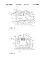
- FIGS. 1 and 2Two well known type of power diode assemblies are shown in FIGS. 1 and 2. The figures have many of the features exaggerated for clarity.
- a first type of power diode assembly 10is shown which is generally employed in light duty automotive applications such as passenger cars.
- Such power diode assemblyincludes a semiconductor rectifier blank 21 (hereafter diode blank), metallic contact members 17 and 25 formed of nickel plated copper and solder layers 19 and 23 joining the metallic contact members to opposite faces of the diode blank 21. Each one of the faces is one of the anode or cathode of the diode.
- the power diode assembly 10is ultrasonically welded or soldered 27 to a heat sink 29 at one of the anode or cathode in accordance with the desired orientation.
- the other of the anode or cathode of power diode assembly 10is soldered 13 to a copper conductor 11.
- a coating of a material 15 such as silicone rubbercompletely encapsulates the power diode assembly to prevent contamination from such things as road salts.
- six such power diode assembliesare used per bridge assembly; three on a first heat sink and thereon a second electrically separate heat sink. Each heat sink is further effective as a DC output terminal.
- a second type of power diode assembly 32is shown as part of an encased diode assembly 30 which is generally employed in heavy duty automotive applications such as commercial vehicles.
- Such power diode assemblyincludes semiconductor rectifier or diode blank 41, and metallic contact member 43 formed of copper or nickel.
- Contact member 43is joined to one face of the diode blank 41 such as by soldering, and the other face of the diode blank is secured to the bottom of metallic case 39 such as by soldering.
- the casethereby is one of the anode or cathode terminals depending upon orientation of the diode blank.
- the other terminalis formed of a conductive lead 45 soldered to the contact member and exiting the case.
- the lead 45takes a serpentine shape for relief of stress upon the power diode assembly 32 and couples to a larger external lead 31.
- a conductive cap 35mates with the case 39 and is sealed 37 from external contaminants.
- the lead 31passes through an aperture in the cap 35, the area therebetween being sealed such as by a glass, epoxy or equivalent material.
- a power diode assembly in accordance with the present inventionincludes a rectifier blank, a pair of contacts and thermally responsive clamping means effective to progressively compressively load the rectifier blank between the first and second contact means as the temperature of the assembly increases.
- the pair of contactshave different temperature dependent rates of thermal expansion and are operatively coupled such that the thermal expansion differential therebetween exerts increasing compressive loads upon the rectifier blank as the assembly temperature increases.
- FIG. 1is a partial sectional schematic view of a prior art diode assembly in a light duty automotive bridge assembly
- FIG. 2is a partial sectional schematic view of a heavy duty diode assembly as used in heavy duty automotive bridge assemblies
- FIG. 3is a first embodiment of a power diode assembly in accord with the present invention.
- FIG. 4is a second embodiment of a power diode assembly in accord with the present invention.
- a diode assembly 60 in accordance with the present inventionis illustrated. Many features of the diode assembly are exaggerated for clarity.
- a diode assemblypreferably comprises an open ended cylindrical metal can 67 having a base 62 and substantially perpendicular side 64 circumferentially surrounding the diode blank. It is further envisioned that two or more substantially symmetrically distributed extensions oriented substantially perpendicular to the base may alternatively be employed in place of a can structure having a circumferentially continuous side wall as described. Such latter structure may be provided, for example, by a stamping having co-planar base and extensions therefrom, which extensions may be bent into substantial perpendicularity with the base portion.
- Can 67is preferably formed from steel, and plated with nickel or copper for proper solder adhesion if desired as described at a later point.
- a diode blank 71is soldered 73 or compressed onto the inside surface of base 62 of can 67, which base provides electrical contact for the diode blank.
- the opposite face of diode blank 71is likewise soldered 69 or compressed onto metallic contact 65 preferably formed of nickel plated copper.
- contact 65has an internal contact portion 65A and a external contact portion 65B.
- Portion 65Ais generally disk-shaped and provides a flange or shoulder around portion 65B.
- Portion 65Bextends above portion 65A and provides for a convenient electrical interface for example to a bridge assembly conductor such as copper conductor 11 as illustrated.
- Surrounding portion 65Bis insulator 63 comprising collar 63A and flange 63B and formed of electrically insulative and substantially incompressible material. It is desirable that the collar portion 63A fits snugly about the outer diameter of portion 65B of contact 65. Furthermore, it is important that flange portion 63B bears against the shoulder of portion 65A of contact 65.
- An exemplary material for ring 63is a thermoplastic such as polyphenylene sulfide.
- Alternative geometriesmay be employed for the contact 65 such as a simple disk.
- alternative insulator geometriessuch as a simple annulus may be substituted for the specific geometry illustrated. It is generally desirable to dispose the insulator at the perimeter of the contact leaving a central aperture through which external electrical interface can be made.
- Alternative means for providing such insulatormay also include direct deposition upon the contact.
- side 64is formed into a lip 68 by rolling or crimping inward against the flange portion 63B of ring 63.
- a compressive loadis created between the lip 68 and the base 62 by such operation.
- FIG. 3further illustrates diode assembly 60 being soldered 75 to heat sink 77.
- Heat sink 77further comprises one of the DC output terminals of the bridge rectifier.
- Copper conductor 11is likewise soldered 61 to external contact portion 65B.
- the exemplary materials chosen for the can 67 and the contact 65 in the present embodimenthave different coefficients of thermal expansion (C t ).
- C tcoefficients of thermal expansion
- copperis used for contact 65 and has a C t of substantially 16.5 while steel is a preferred material used for the can 67 and has a C t of substantially 12. It is necessary that the C t of the contact be greater than the C t of the can.
- the cooperation between the operatively coupled contactsprovides for a thermally responsive clamp upon the diode blank with generally increasing compressive loads for increasing assembly temperatures. Such increasing temperatures are generally the result of internally generated heat.
- the inventorhas demonstrated through experimentation that applying compressive forces to power semiconductor solder interfaces increases the fatigue life thereat.
- FIG. 4shows a diode assembly 80 in accordance with the present invention.
- the diode assemblyalso comprises a cylindrical metallic can 67 having a base 62 and substantially perpendicular sides 64.
- a diode blank 71is soldered 73 or compressed onto one face thereof directly to the inside surface of base 62 of can 67.
- the opposite face of diode blank 71is likewise soldered 69 or compressed onto metallic contact 65.
- the materials used in this embodimentmay be the same as those used in the previous embodiment.
- the contact 81has geometry similar to that of the contact of the previously described embodiment; that is to say it comprises an internal contact portion 81B and an external contact portion 81A which provides for an electrical lead.
- Portion 81Bprovides a major surface against which bears insulator 63.
- Contact 81may be fabricated for example as a headed copper part.
- the remaining features illustrated in FIG. 4 that are labeled similar to items in FIG. 3may be considered as being substantially equivalent thereto.
- the embodiment of the diode assembly illustrated in FIG. 4is shown soldered to a heat sink/conductor 77 similar to the embodiment shown in FIG. 3.
- the diode assembly 80may be suitably sized for a retentive press fit into a heat sink/conductor such that the outer surfaces of sides 64 are enclosed and dissipate heat to the surrounding heat sink.
- One or both of the mating surfacesmay be scored or fluted to facilitate a press fit operation.
- the present inventionis equally applicable to a solderless interface of the can and contact to respective faces of the diode blank.
- the progressive compressive force with temperature increasefurther insures contact integrity at the electrical interfaces of the diode blank.
Landscapes
- Physics & Mathematics (AREA)
- Condensed Matter Physics & Semiconductors (AREA)
- General Physics & Mathematics (AREA)
- Engineering & Computer Science (AREA)
- Computer Hardware Design (AREA)
- Microelectronics & Electronic Packaging (AREA)
- Power Engineering (AREA)
- Rectifiers (AREA)
- Thermistors And Varistors (AREA)
- Synchronous Machinery (AREA)
Abstract
Description
Claims (8)
Priority Applications (4)
| Application Number | Priority Date | Filing Date | Title |
|---|---|---|---|
| US08/656,956US5773885A (en) | 1996-06-06 | 1996-06-06 | Thermally responsive compressive diode assembly |
| EP97201410AEP0812014A3 (en) | 1996-06-06 | 1997-05-09 | Power rectifier assembly |
| MX9703825AMX9703825A (en) | 1996-06-06 | 1997-05-23 | Thermally responsive compressive diode assembly. |
| JP9149478AJP2802268B2 (en) | 1996-06-06 | 1997-06-06 | Thermal response compression type diode assembly |
Applications Claiming Priority (1)
| Application Number | Priority Date | Filing Date | Title |
|---|---|---|---|
| US08/656,956US5773885A (en) | 1996-06-06 | 1996-06-06 | Thermally responsive compressive diode assembly |
Publications (1)
| Publication Number | Publication Date |
|---|---|
| US5773885Atrue US5773885A (en) | 1998-06-30 |
Family
ID=24635286
Family Applications (1)
| Application Number | Title | Priority Date | Filing Date |
|---|---|---|---|
| US08/656,956Expired - LifetimeUS5773885A (en) | 1996-06-06 | 1996-06-06 | Thermally responsive compressive diode assembly |
Country Status (4)
| Country | Link |
|---|---|
| US (1) | US5773885A (en) |
| EP (1) | EP0812014A3 (en) |
| JP (1) | JP2802268B2 (en) |
| MX (1) | MX9703825A (en) |
Cited By (4)
| Publication number | Priority date | Publication date | Assignee | Title |
|---|---|---|---|---|
| US20040014256A1 (en)* | 2000-08-28 | 2004-01-22 | Transpo Electronics, Inc. | Method for manufacturing diode subassemblies used in rectifier assemblies of engine driven generators |
| US20060214291A1 (en)* | 2005-03-25 | 2006-09-28 | Koji Sasaki | Semiconductor device |
| US20070182023A1 (en)* | 2006-02-08 | 2007-08-09 | Hitachi, Ltd. | Semiconductor device |
| CN113271038A (en)* | 2021-04-16 | 2021-08-17 | 东南大学 | Bridge type thermal rectifier |
Families Citing this family (2)
| Publication number | Priority date | Publication date | Assignee | Title |
|---|---|---|---|---|
| DE19856332A1 (en)* | 1998-12-07 | 2000-06-15 | Bosch Gmbh Robert | Electronic component housing, e.g. for a Gunn diode of a distance radar for an automobile adaptive cruise control system, comprises a cover with an integral contact spring for electrically contacting the component |
| JP2015142018A (en)* | 2014-01-29 | 2015-08-03 | 三菱電機株式会社 | Power semiconductor device |
Citations (1)
| Publication number | Priority date | Publication date | Assignee | Title |
|---|---|---|---|---|
| US5302856A (en)* | 1990-10-08 | 1994-04-12 | Hitachi, Ltd. | Semiconductor rectifying device and full-wave rectifier fabricated using the same |
Family Cites Families (3)
| Publication number | Priority date | Publication date | Assignee | Title |
|---|---|---|---|---|
| JPS58161A (en)* | 1981-06-25 | 1983-01-05 | Fujitsu Ltd | semiconductor equipment |
| JPS58128758A (en)* | 1982-01-27 | 1983-08-01 | Hitachi Ltd | Semiconductor device and its manufacture |
| JPH0851169A (en)* | 1994-08-08 | 1996-02-20 | Fuji Electric Co Ltd | Semiconductor device |
- 1996
- 1996-06-06USUS08/656,956patent/US5773885A/ennot_activeExpired - Lifetime
- 1997
- 1997-05-09EPEP97201410Apatent/EP0812014A3/ennot_activeWithdrawn
- 1997-05-23MXMX9703825Apatent/MX9703825A/enunknown
- 1997-06-06JPJP9149478Apatent/JP2802268B2/ennot_activeExpired - Lifetime
Patent Citations (1)
| Publication number | Priority date | Publication date | Assignee | Title |
|---|---|---|---|---|
| US5302856A (en)* | 1990-10-08 | 1994-04-12 | Hitachi, Ltd. | Semiconductor rectifying device and full-wave rectifier fabricated using the same |
Non-Patent Citations (2)
| Title |
|---|
| Training Chart Manual; Delco Remy, Anderson, Indiana; 1962; pp. Chart 13; "Delcotron generator and the charging circuit". |
| Training Chart Manual; Delco Remy, Anderson, Indiana; 1962; pp. Chart 13; Delcotron generator and the charging circuit .* |
Cited By (7)
| Publication number | Priority date | Publication date | Assignee | Title |
|---|---|---|---|---|
| US20040014256A1 (en)* | 2000-08-28 | 2004-01-22 | Transpo Electronics, Inc. | Method for manufacturing diode subassemblies used in rectifier assemblies of engine driven generators |
| US7060533B2 (en)* | 2000-08-28 | 2006-06-13 | Wetherill Associates, Inc. | Method for manufacturing diode subassemblies used in rectifier assemblies of engine driven generators |
| US20060214291A1 (en)* | 2005-03-25 | 2006-09-28 | Koji Sasaki | Semiconductor device |
| US7193319B2 (en)* | 2005-03-25 | 2007-03-20 | Hitachi, Ltd. | Semiconductor device |
| US20070182023A1 (en)* | 2006-02-08 | 2007-08-09 | Hitachi, Ltd. | Semiconductor device |
| CN113271038A (en)* | 2021-04-16 | 2021-08-17 | 东南大学 | Bridge type thermal rectifier |
| CN113271038B (en)* | 2021-04-16 | 2022-06-17 | 东南大学 | Bridge type thermal rectifier |
Also Published As
| Publication number | Publication date |
|---|---|
| EP0812014A2 (en) | 1997-12-10 |
| EP0812014A3 (en) | 1999-09-22 |
| MX9703825A (en) | 1997-12-31 |
| JPH1074875A (en) | 1998-03-17 |
| JP2802268B2 (en) | 1998-09-24 |
Similar Documents
| Publication | Publication Date | Title |
|---|---|---|
| US6528911B1 (en) | Rectifier assembly for automotive alternators | |
| US3221219A (en) | Semiconductor device having a nickel surface in pressure sliding engagement with a silver surface | |
| US5659212A (en) | Rectifier assembly for automotive alternator | |
| US4956696A (en) | Compression loaded semiconductor device | |
| US3736474A (en) | Solderless semiconductor devices | |
| CN1879212B (en) | diode | |
| EP0100626A2 (en) | Semi-conductor assembly | |
| US3413532A (en) | Compression bonded semiconductor device | |
| US5652471A (en) | Rectifier arrangement, especially for a three-phase generator for a motor vehicle | |
| US5773885A (en) | Thermally responsive compressive diode assembly | |
| US2744218A (en) | Sealed rectifier unit and method of making the same | |
| US3651383A (en) | Unitary high power semiconductor subassembly suitable for mounting on a separable heat sink | |
| JP4424199B2 (en) | Semiconductor device | |
| US3992717A (en) | Housing for a compression bonded encapsulation of a semiconductor device | |
| US3280387A (en) | Encapsuled semiconductor with alloy-bonded carrier plates and pressure maintained connectors | |
| EP0194946A2 (en) | Pressurized contact type double gate static induction thyristor | |
| US3793570A (en) | Compact power semiconductor device and method of making same | |
| US3434018A (en) | Heat conductive mounting base for a semiconductor device | |
| US4881118A (en) | Semiconductor device | |
| US3450962A (en) | Pressure electrical contact assembly for a semiconductor device | |
| US4724474A (en) | Power bridge rectifier assembly | |
| US3280383A (en) | Electronic semiconductor device | |
| US4063348A (en) | Unique packaging method for use on large semiconductor devices | |
| US20040066106A1 (en) | Plastic fastener | |
| US4068368A (en) | Closure for semiconductor device and method of construction |
Legal Events
| Date | Code | Title | Description |
|---|---|---|---|
| AS | Assignment | Owner name:GENERAL MOTORS CORPORATION, MICHIGAN Free format text:ASSIGNMENT OF ASSIGNORS INTEREST;ASSIGNOR:STEELE, ROY BURTON;REEL/FRAME:008242/0769 Effective date:19960524 | |
| REMI | Maintenance fee reminder mailed | ||
| AS | Assignment | Owner name:DELPHI TECHNOLOGIES, INC., MICHIGAN Free format text:ASSIGNMENT OF ASSIGNORS INTEREST;ASSIGNOR:GENERAL MOTORS CORPORATION;REEL/FRAME:012745/0724 Effective date:20020212 | |
| REIN | Reinstatement after maintenance fee payment confirmed | ||
| FP | Lapsed due to failure to pay maintenance fee | Effective date:20020630 | |
| FEPP | Fee payment procedure | Free format text:PETITION RELATED TO MAINTENANCE FEES FILED (ORIGINAL EVENT CODE: PMFP); ENTITY STATUS OF PATENT OWNER: LARGE ENTITY | |
| FEPP | Fee payment procedure | Free format text:PETITION RELATED TO MAINTENANCE FEES GRANTED (ORIGINAL EVENT CODE: PMFG); ENTITY STATUS OF PATENT OWNER: LARGE ENTITY | |
| FPAY | Fee payment | Year of fee payment:4 | |
| SULP | Surcharge for late payment | ||
| PRDP | Patent reinstated due to the acceptance of a late maintenance fee | Effective date:20030203 | |
| STCF | Information on status: patent grant | Free format text:PATENTED CASE | |
| AS | Assignment | Owner name:DEUTSCHE BANK NATIONAL TRUST COMANY, AS COLLATERAL Free format text:SECURITY AGREEMENT;ASSIGNOR:DELCO REMY INTERNATIONAL, INC.;REEL/FRAME:015377/0076 Effective date:20040423 | |
| FPAY | Fee payment | Year of fee payment:8 | |
| FPAY | Fee payment | Year of fee payment:12 | |
| AS | Assignment | Owner name:REMY TECHNOLOGIES, LLC, INDIANA Free format text:ASSIGNMENT OF ASSIGNORS INTEREST;ASSIGNOR:DELPHI TECHNOLOGIES, INC.;REEL/FRAME:025114/0809 Effective date:20101005 | |
| AS | Assignment | Owner name:BANK OF AMERICA, N.A., AS ADMINISTRATIVE AGENT, NO Free format text:GRANT OF PATENT SECURITY INTEREST;ASSIGNOR:REMY TECHNOLOGIES, L.L.C.;REEL/FRAME:025521/0387 Effective date:20101217 | |
| AS | Assignment | Owner name:WELLS FARGO CAPITAL FINANCE, LLC, AS AGENT, ILLINO Free format text:SECURITY AGREEMENT;ASSIGNORS:REMY TECHNOLOGIES, L.L.C.;REMY POWER PRODUCTS, LLC;REEL/FRAME:025525/0186 Effective date:20101217 | |
| AS | Assignment | Owner name:REMY INTERNATIONAL INC. (F/K/A DELCO REMY INTERNAT Free format text:RELEASE BY SECURED PARTY;ASSIGNOR:DEUTSCHE BANK NATIONAL TRUST COMPANY;REEL/FRAME:037075/0029 Effective date:20080428 Owner name:REMY TECHNOLOGIES, L.L.C., INDIANA Free format text:RELEASE BY SECURED PARTY;ASSIGNOR:DEUTSCHE BANK NATIONAL TRUST COMPANY;REEL/FRAME:037075/0029 Effective date:20080428 Owner name:REMY INC. (F/K/A DELCO REMY AMERICA INC.), INDIANA Free format text:RELEASE BY SECURED PARTY;ASSIGNOR:DEUTSCHE BANK NATIONAL TRUST COMPANY;REEL/FRAME:037075/0029 Effective date:20080428 | |
| AS | Assignment | Owner name:REMY TECHNOLOGIES, L.L.C., INDIANA Free format text:RELEASE OF SECURITY INTEREST IN PATENTS PREVIOUSLY RECORDED AT REEL/FRAME 025521/0387;ASSIGNOR:BANK OF AMERICA, N.A.;REEL/FRAME:037101/0125 Effective date:20151110 Owner name:REMY POWER PRODUCTS, L.L.C., INDIANA Free format text:RELEASE OF SECURITY INTEREST IN PATENTS PREVIOUSLY RECORDED AT REEL/FRAME 025525/0186;ASSIGNOR:WELLS FARGO CAPITAL FINANCE, L.L.C.;REEL/FRAME:037108/0618 Effective date:20151110 Owner name:REMY TECHNOLOGIES, L.L.C., INDIANA Free format text:RELEASE OF SECURITY INTEREST IN PATENTS PREVIOUSLY RECORDED AT REEL/FRAME 025525/0186;ASSIGNOR:WELLS FARGO CAPITAL FINANCE, L.L.C.;REEL/FRAME:037108/0618 Effective date:20151110 |