US5773359A - Interconnect system and method of fabrication - Google Patents
Interconnect system and method of fabricationDownload PDFInfo
- Publication number
- US5773359A US5773359AUS08/578,255US57825595AUS5773359AUS 5773359 AUS5773359 AUS 5773359AUS 57825595 AUS57825595 AUS 57825595AUS 5773359 AUS5773359 AUS 5773359A
- Authority
- US
- United States
- Prior art keywords
- layer
- interconnect
- over
- adhesion
- barrier
- Prior art date
- Legal status (The legal status is an assumption and is not a legal conclusion. Google has not performed a legal analysis and makes no representation as to the accuracy of the status listed.)
- Expired - Lifetime
Links
Images
Classifications
- H—ELECTRICITY
- H01—ELECTRIC ELEMENTS
- H01L—SEMICONDUCTOR DEVICES NOT COVERED BY CLASS H10
- H01L24/00—Arrangements for connecting or disconnecting semiconductor or solid-state bodies; Methods or apparatus related thereto
- H01L24/01—Means for bonding being attached to, or being formed on, the surface to be connected, e.g. chip-to-package, die-attach, "first-level" interconnects; Manufacturing methods related thereto
- H01L24/10—Bump connectors ; Manufacturing methods related thereto
- H01L24/11—Manufacturing methods
- H—ELECTRICITY
- H01—ELECTRIC ELEMENTS
- H01L—SEMICONDUCTOR DEVICES NOT COVERED BY CLASS H10
- H01L24/00—Arrangements for connecting or disconnecting semiconductor or solid-state bodies; Methods or apparatus related thereto
- H01L24/01—Means for bonding being attached to, or being formed on, the surface to be connected, e.g. chip-to-package, die-attach, "first-level" interconnects; Manufacturing methods related thereto
- H01L24/02—Bonding areas ; Manufacturing methods related thereto
- H01L24/04—Structure, shape, material or disposition of the bonding areas prior to the connecting process
- H01L24/05—Structure, shape, material or disposition of the bonding areas prior to the connecting process of an individual bonding area
- H—ELECTRICITY
- H01—ELECTRIC ELEMENTS
- H01L—SEMICONDUCTOR DEVICES NOT COVERED BY CLASS H10
- H01L2224/00—Indexing scheme for arrangements for connecting or disconnecting semiconductor or solid-state bodies and methods related thereto as covered by H01L24/00
- H01L2224/01—Means for bonding being attached to, or being formed on, the surface to be connected, e.g. chip-to-package, die-attach, "first-level" interconnects; Manufacturing methods related thereto
- H01L2224/02—Bonding areas; Manufacturing methods related thereto
- H01L2224/03—Manufacturing methods
- H01L2224/039—Methods of manufacturing bonding areas involving a specific sequence of method steps
- H01L2224/03912—Methods of manufacturing bonding areas involving a specific sequence of method steps the bump being used as a mask for patterning the bonding area
- H—ELECTRICITY
- H01—ELECTRIC ELEMENTS
- H01L—SEMICONDUCTOR DEVICES NOT COVERED BY CLASS H10
- H01L2224/00—Indexing scheme for arrangements for connecting or disconnecting semiconductor or solid-state bodies and methods related thereto as covered by H01L24/00
- H01L2224/01—Means for bonding being attached to, or being formed on, the surface to be connected, e.g. chip-to-package, die-attach, "first-level" interconnects; Manufacturing methods related thereto
- H01L2224/02—Bonding areas; Manufacturing methods related thereto
- H01L2224/04—Structure, shape, material or disposition of the bonding areas prior to the connecting process
- H01L2224/0401—Bonding areas specifically adapted for bump connectors, e.g. under bump metallisation [UBM]
- H—ELECTRICITY
- H01—ELECTRIC ELEMENTS
- H01L—SEMICONDUCTOR DEVICES NOT COVERED BY CLASS H10
- H01L2224/00—Indexing scheme for arrangements for connecting or disconnecting semiconductor or solid-state bodies and methods related thereto as covered by H01L24/00
- H01L2224/01—Means for bonding being attached to, or being formed on, the surface to be connected, e.g. chip-to-package, die-attach, "first-level" interconnects; Manufacturing methods related thereto
- H01L2224/02—Bonding areas; Manufacturing methods related thereto
- H01L2224/04—Structure, shape, material or disposition of the bonding areas prior to the connecting process
- H01L2224/05—Structure, shape, material or disposition of the bonding areas prior to the connecting process of an individual bonding area
- H01L2224/05001—Internal layers
- H01L2224/0502—Disposition
- H01L2224/05026—Disposition the internal layer being disposed in a recess of the surface
- H01L2224/05027—Disposition the internal layer being disposed in a recess of the surface the internal layer extending out of an opening
- H—ELECTRICITY
- H01—ELECTRIC ELEMENTS
- H01L—SEMICONDUCTOR DEVICES NOT COVERED BY CLASS H10
- H01L2224/00—Indexing scheme for arrangements for connecting or disconnecting semiconductor or solid-state bodies and methods related thereto as covered by H01L24/00
- H01L2224/01—Means for bonding being attached to, or being formed on, the surface to be connected, e.g. chip-to-package, die-attach, "first-level" interconnects; Manufacturing methods related thereto
- H01L2224/02—Bonding areas; Manufacturing methods related thereto
- H01L2224/04—Structure, shape, material or disposition of the bonding areas prior to the connecting process
- H01L2224/05—Structure, shape, material or disposition of the bonding areas prior to the connecting process of an individual bonding area
- H01L2224/05001—Internal layers
- H01L2224/05099—Material
- H01L2224/051—Material with a principal constituent of the material being a metal or a metalloid, e.g. boron [B], silicon [Si], germanium [Ge], arsenic [As], antimony [Sb], tellurium [Te] and polonium [Po], and alloys thereof
- H01L2224/05117—Material with a principal constituent of the material being a metal or a metalloid, e.g. boron [B], silicon [Si], germanium [Ge], arsenic [As], antimony [Sb], tellurium [Te] and polonium [Po], and alloys thereof the principal constituent melting at a temperature of greater than or equal to 400°C and less than 950°C
- H01L2224/05124—Aluminium [Al] as principal constituent
- H—ELECTRICITY
- H01—ELECTRIC ELEMENTS
- H01L—SEMICONDUCTOR DEVICES NOT COVERED BY CLASS H10
- H01L2224/00—Indexing scheme for arrangements for connecting or disconnecting semiconductor or solid-state bodies and methods related thereto as covered by H01L24/00
- H01L2224/01—Means for bonding being attached to, or being formed on, the surface to be connected, e.g. chip-to-package, die-attach, "first-level" interconnects; Manufacturing methods related thereto
- H01L2224/02—Bonding areas; Manufacturing methods related thereto
- H01L2224/04—Structure, shape, material or disposition of the bonding areas prior to the connecting process
- H01L2224/05—Structure, shape, material or disposition of the bonding areas prior to the connecting process of an individual bonding area
- H01L2224/05001—Internal layers
- H01L2224/05099—Material
- H01L2224/051—Material with a principal constituent of the material being a metal or a metalloid, e.g. boron [B], silicon [Si], germanium [Ge], arsenic [As], antimony [Sb], tellurium [Te] and polonium [Po], and alloys thereof
- H01L2224/05138—Material with a principal constituent of the material being a metal or a metalloid, e.g. boron [B], silicon [Si], germanium [Ge], arsenic [As], antimony [Sb], tellurium [Te] and polonium [Po], and alloys thereof the principal constituent melting at a temperature of greater than or equal to 950°C and less than 1550°C
- H01L2224/05147—Copper [Cu] as principal constituent
- H—ELECTRICITY
- H01—ELECTRIC ELEMENTS
- H01L—SEMICONDUCTOR DEVICES NOT COVERED BY CLASS H10
- H01L2224/00—Indexing scheme for arrangements for connecting or disconnecting semiconductor or solid-state bodies and methods related thereto as covered by H01L24/00
- H01L2224/01—Means for bonding being attached to, or being formed on, the surface to be connected, e.g. chip-to-package, die-attach, "first-level" interconnects; Manufacturing methods related thereto
- H01L2224/02—Bonding areas; Manufacturing methods related thereto
- H01L2224/04—Structure, shape, material or disposition of the bonding areas prior to the connecting process
- H01L2224/05—Structure, shape, material or disposition of the bonding areas prior to the connecting process of an individual bonding area
- H01L2224/05001—Internal layers
- H01L2224/05099—Material
- H01L2224/051—Material with a principal constituent of the material being a metal or a metalloid, e.g. boron [B], silicon [Si], germanium [Ge], arsenic [As], antimony [Sb], tellurium [Te] and polonium [Po], and alloys thereof
- H01L2224/05138—Material with a principal constituent of the material being a metal or a metalloid, e.g. boron [B], silicon [Si], germanium [Ge], arsenic [As], antimony [Sb], tellurium [Te] and polonium [Po], and alloys thereof the principal constituent melting at a temperature of greater than or equal to 950°C and less than 1550°C
- H01L2224/05155—Nickel [Ni] as principal constituent
- H—ELECTRICITY
- H01—ELECTRIC ELEMENTS
- H01L—SEMICONDUCTOR DEVICES NOT COVERED BY CLASS H10
- H01L2224/00—Indexing scheme for arrangements for connecting or disconnecting semiconductor or solid-state bodies and methods related thereto as covered by H01L24/00
- H01L2224/01—Means for bonding being attached to, or being formed on, the surface to be connected, e.g. chip-to-package, die-attach, "first-level" interconnects; Manufacturing methods related thereto
- H01L2224/02—Bonding areas; Manufacturing methods related thereto
- H01L2224/04—Structure, shape, material or disposition of the bonding areas prior to the connecting process
- H01L2224/05—Structure, shape, material or disposition of the bonding areas prior to the connecting process of an individual bonding area
- H01L2224/05001—Internal layers
- H01L2224/05099—Material
- H01L2224/051—Material with a principal constituent of the material being a metal or a metalloid, e.g. boron [B], silicon [Si], germanium [Ge], arsenic [As], antimony [Sb], tellurium [Te] and polonium [Po], and alloys thereof
- H01L2224/05163—Material with a principal constituent of the material being a metal or a metalloid, e.g. boron [B], silicon [Si], germanium [Ge], arsenic [As], antimony [Sb], tellurium [Te] and polonium [Po], and alloys thereof the principal constituent melting at a temperature of greater than 1550°C
- H01L2224/05166—Titanium [Ti] as principal constituent
- H—ELECTRICITY
- H01—ELECTRIC ELEMENTS
- H01L—SEMICONDUCTOR DEVICES NOT COVERED BY CLASS H10
- H01L2224/00—Indexing scheme for arrangements for connecting or disconnecting semiconductor or solid-state bodies and methods related thereto as covered by H01L24/00
- H01L2224/01—Means for bonding being attached to, or being formed on, the surface to be connected, e.g. chip-to-package, die-attach, "first-level" interconnects; Manufacturing methods related thereto
- H01L2224/02—Bonding areas; Manufacturing methods related thereto
- H01L2224/04—Structure, shape, material or disposition of the bonding areas prior to the connecting process
- H01L2224/05—Structure, shape, material or disposition of the bonding areas prior to the connecting process of an individual bonding area
- H01L2224/05001—Internal layers
- H01L2224/05099—Material
- H01L2224/051—Material with a principal constituent of the material being a metal or a metalloid, e.g. boron [B], silicon [Si], germanium [Ge], arsenic [As], antimony [Sb], tellurium [Te] and polonium [Po], and alloys thereof
- H01L2224/05163—Material with a principal constituent of the material being a metal or a metalloid, e.g. boron [B], silicon [Si], germanium [Ge], arsenic [As], antimony [Sb], tellurium [Te] and polonium [Po], and alloys thereof the principal constituent melting at a temperature of greater than 1550°C
- H01L2224/05171—Chromium [Cr] as principal constituent
- H—ELECTRICITY
- H01—ELECTRIC ELEMENTS
- H01L—SEMICONDUCTOR DEVICES NOT COVERED BY CLASS H10
- H01L2224/00—Indexing scheme for arrangements for connecting or disconnecting semiconductor or solid-state bodies and methods related thereto as covered by H01L24/00
- H01L2224/01—Means for bonding being attached to, or being formed on, the surface to be connected, e.g. chip-to-package, die-attach, "first-level" interconnects; Manufacturing methods related thereto
- H01L2224/02—Bonding areas; Manufacturing methods related thereto
- H01L2224/04—Structure, shape, material or disposition of the bonding areas prior to the connecting process
- H01L2224/05—Structure, shape, material or disposition of the bonding areas prior to the connecting process of an individual bonding area
- H01L2224/05001—Internal layers
- H01L2224/05099—Material
- H01L2224/051—Material with a principal constituent of the material being a metal or a metalloid, e.g. boron [B], silicon [Si], germanium [Ge], arsenic [As], antimony [Sb], tellurium [Te] and polonium [Po], and alloys thereof
- H01L2224/05163—Material with a principal constituent of the material being a metal or a metalloid, e.g. boron [B], silicon [Si], germanium [Ge], arsenic [As], antimony [Sb], tellurium [Te] and polonium [Po], and alloys thereof the principal constituent melting at a temperature of greater than 1550°C
- H01L2224/05184—Tungsten [W] as principal constituent
- H—ELECTRICITY
- H01—ELECTRIC ELEMENTS
- H01L—SEMICONDUCTOR DEVICES NOT COVERED BY CLASS H10
- H01L2224/00—Indexing scheme for arrangements for connecting or disconnecting semiconductor or solid-state bodies and methods related thereto as covered by H01L24/00
- H01L2224/01—Means for bonding being attached to, or being formed on, the surface to be connected, e.g. chip-to-package, die-attach, "first-level" interconnects; Manufacturing methods related thereto
- H01L2224/02—Bonding areas; Manufacturing methods related thereto
- H01L2224/04—Structure, shape, material or disposition of the bonding areas prior to the connecting process
- H01L2224/05—Structure, shape, material or disposition of the bonding areas prior to the connecting process of an individual bonding area
- H01L2224/0554—External layer
- H01L2224/0556—Disposition
- H01L2224/05571—Disposition the external layer being disposed in a recess of the surface
- H01L2224/05572—Disposition the external layer being disposed in a recess of the surface the external layer extending out of an opening
- H—ELECTRICITY
- H01—ELECTRIC ELEMENTS
- H01L—SEMICONDUCTOR DEVICES NOT COVERED BY CLASS H10
- H01L2224/00—Indexing scheme for arrangements for connecting or disconnecting semiconductor or solid-state bodies and methods related thereto as covered by H01L24/00
- H01L2224/01—Means for bonding being attached to, or being formed on, the surface to be connected, e.g. chip-to-package, die-attach, "first-level" interconnects; Manufacturing methods related thereto
- H01L2224/02—Bonding areas; Manufacturing methods related thereto
- H01L2224/04—Structure, shape, material or disposition of the bonding areas prior to the connecting process
- H01L2224/05—Structure, shape, material or disposition of the bonding areas prior to the connecting process of an individual bonding area
- H01L2224/0554—External layer
- H01L2224/05599—Material
- H01L2224/056—Material with a principal constituent of the material being a metal or a metalloid, e.g. boron [B], silicon [Si], germanium [Ge], arsenic [As], antimony [Sb], tellurium [Te] and polonium [Po], and alloys thereof
- H01L2224/05638—Material with a principal constituent of the material being a metal or a metalloid, e.g. boron [B], silicon [Si], germanium [Ge], arsenic [As], antimony [Sb], tellurium [Te] and polonium [Po], and alloys thereof the principal constituent melting at a temperature of greater than or equal to 950°C and less than 1550°C
- H01L2224/05647—Copper [Cu] as principal constituent
- H—ELECTRICITY
- H01—ELECTRIC ELEMENTS
- H01L—SEMICONDUCTOR DEVICES NOT COVERED BY CLASS H10
- H01L2224/00—Indexing scheme for arrangements for connecting or disconnecting semiconductor or solid-state bodies and methods related thereto as covered by H01L24/00
- H01L2224/01—Means for bonding being attached to, or being formed on, the surface to be connected, e.g. chip-to-package, die-attach, "first-level" interconnects; Manufacturing methods related thereto
- H01L2224/10—Bump connectors; Manufacturing methods related thereto
- H01L2224/11—Manufacturing methods
- H01L2224/114—Manufacturing methods by blanket deposition of the material of the bump connector
- H—ELECTRICITY
- H01—ELECTRIC ELEMENTS
- H01L—SEMICONDUCTOR DEVICES NOT COVERED BY CLASS H10
- H01L2224/00—Indexing scheme for arrangements for connecting or disconnecting semiconductor or solid-state bodies and methods related thereto as covered by H01L24/00
- H01L2224/01—Means for bonding being attached to, or being formed on, the surface to be connected, e.g. chip-to-package, die-attach, "first-level" interconnects; Manufacturing methods related thereto
- H01L2224/10—Bump connectors; Manufacturing methods related thereto
- H01L2224/11—Manufacturing methods
- H01L2224/116—Manufacturing methods by patterning a pre-deposited material
- H—ELECTRICITY
- H01—ELECTRIC ELEMENTS
- H01L—SEMICONDUCTOR DEVICES NOT COVERED BY CLASS H10
- H01L2224/00—Indexing scheme for arrangements for connecting or disconnecting semiconductor or solid-state bodies and methods related thereto as covered by H01L24/00
- H01L2224/01—Means for bonding being attached to, or being formed on, the surface to be connected, e.g. chip-to-package, die-attach, "first-level" interconnects; Manufacturing methods related thereto
- H01L2224/10—Bump connectors; Manufacturing methods related thereto
- H01L2224/12—Structure, shape, material or disposition of the bump connectors prior to the connecting process
- H01L2224/13—Structure, shape, material or disposition of the bump connectors prior to the connecting process of an individual bump connector
- H01L2224/13001—Core members of the bump connector
- H01L2224/13099—Material
- H—ELECTRICITY
- H01—ELECTRIC ELEMENTS
- H01L—SEMICONDUCTOR DEVICES NOT COVERED BY CLASS H10
- H01L2924/00—Indexing scheme for arrangements or methods for connecting or disconnecting semiconductor or solid-state bodies as covered by H01L24/00
- H01L2924/01—Chemical elements
- H01L2924/01004—Beryllium [Be]
- H—ELECTRICITY
- H01—ELECTRIC ELEMENTS
- H01L—SEMICONDUCTOR DEVICES NOT COVERED BY CLASS H10
- H01L2924/00—Indexing scheme for arrangements or methods for connecting or disconnecting semiconductor or solid-state bodies as covered by H01L24/00
- H01L2924/01—Chemical elements
- H01L2924/01006—Carbon [C]
- H—ELECTRICITY
- H01—ELECTRIC ELEMENTS
- H01L—SEMICONDUCTOR DEVICES NOT COVERED BY CLASS H10
- H01L2924/00—Indexing scheme for arrangements or methods for connecting or disconnecting semiconductor or solid-state bodies as covered by H01L24/00
- H01L2924/01—Chemical elements
- H01L2924/01013—Aluminum [Al]
- H—ELECTRICITY
- H01—ELECTRIC ELEMENTS
- H01L—SEMICONDUCTOR DEVICES NOT COVERED BY CLASS H10
- H01L2924/00—Indexing scheme for arrangements or methods for connecting or disconnecting semiconductor or solid-state bodies as covered by H01L24/00
- H01L2924/01—Chemical elements
- H01L2924/01022—Titanium [Ti]
- H—ELECTRICITY
- H01—ELECTRIC ELEMENTS
- H01L—SEMICONDUCTOR DEVICES NOT COVERED BY CLASS H10
- H01L2924/00—Indexing scheme for arrangements or methods for connecting or disconnecting semiconductor or solid-state bodies as covered by H01L24/00
- H01L2924/01—Chemical elements
- H01L2924/01029—Copper [Cu]
- H—ELECTRICITY
- H01—ELECTRIC ELEMENTS
- H01L—SEMICONDUCTOR DEVICES NOT COVERED BY CLASS H10
- H01L2924/00—Indexing scheme for arrangements or methods for connecting or disconnecting semiconductor or solid-state bodies as covered by H01L24/00
- H01L2924/01—Chemical elements
- H01L2924/01033—Arsenic [As]
- H—ELECTRICITY
- H01—ELECTRIC ELEMENTS
- H01L—SEMICONDUCTOR DEVICES NOT COVERED BY CLASS H10
- H01L2924/00—Indexing scheme for arrangements or methods for connecting or disconnecting semiconductor or solid-state bodies as covered by H01L24/00
- H01L2924/01—Chemical elements
- H01L2924/01039—Yttrium [Y]
- H—ELECTRICITY
- H01—ELECTRIC ELEMENTS
- H01L—SEMICONDUCTOR DEVICES NOT COVERED BY CLASS H10
- H01L2924/00—Indexing scheme for arrangements or methods for connecting or disconnecting semiconductor or solid-state bodies as covered by H01L24/00
- H01L2924/01—Chemical elements
- H01L2924/01042—Molybdenum [Mo]
- H—ELECTRICITY
- H01—ELECTRIC ELEMENTS
- H01L—SEMICONDUCTOR DEVICES NOT COVERED BY CLASS H10
- H01L2924/00—Indexing scheme for arrangements or methods for connecting or disconnecting semiconductor or solid-state bodies as covered by H01L24/00
- H01L2924/01—Chemical elements
- H01L2924/01049—Indium [In]
- H—ELECTRICITY
- H01—ELECTRIC ELEMENTS
- H01L—SEMICONDUCTOR DEVICES NOT COVERED BY CLASS H10
- H01L2924/00—Indexing scheme for arrangements or methods for connecting or disconnecting semiconductor or solid-state bodies as covered by H01L24/00
- H01L2924/01—Chemical elements
- H01L2924/01074—Tungsten [W]
- H—ELECTRICITY
- H01—ELECTRIC ELEMENTS
- H01L—SEMICONDUCTOR DEVICES NOT COVERED BY CLASS H10
- H01L2924/00—Indexing scheme for arrangements or methods for connecting or disconnecting semiconductor or solid-state bodies as covered by H01L24/00
- H01L2924/01—Chemical elements
- H01L2924/01078—Platinum [Pt]
- H—ELECTRICITY
- H01—ELECTRIC ELEMENTS
- H01L—SEMICONDUCTOR DEVICES NOT COVERED BY CLASS H10
- H01L2924/00—Indexing scheme for arrangements or methods for connecting or disconnecting semiconductor or solid-state bodies as covered by H01L24/00
- H01L2924/01—Chemical elements
- H01L2924/01079—Gold [Au]
- H—ELECTRICITY
- H01—ELECTRIC ELEMENTS
- H01L—SEMICONDUCTOR DEVICES NOT COVERED BY CLASS H10
- H01L2924/00—Indexing scheme for arrangements or methods for connecting or disconnecting semiconductor or solid-state bodies as covered by H01L24/00
- H01L2924/01—Chemical elements
- H01L2924/01082—Lead [Pb]
- H—ELECTRICITY
- H01—ELECTRIC ELEMENTS
- H01L—SEMICONDUCTOR DEVICES NOT COVERED BY CLASS H10
- H01L2924/00—Indexing scheme for arrangements or methods for connecting or disconnecting semiconductor or solid-state bodies as covered by H01L24/00
- H01L2924/013—Alloys
- H01L2924/0132—Binary Alloys
- H01L2924/01327—Intermediate phases, i.e. intermetallics compounds
- H—ELECTRICITY
- H01—ELECTRIC ELEMENTS
- H01L—SEMICONDUCTOR DEVICES NOT COVERED BY CLASS H10
- H01L2924/00—Indexing scheme for arrangements or methods for connecting or disconnecting semiconductor or solid-state bodies as covered by H01L24/00
- H01L2924/013—Alloys
- H01L2924/014—Solder alloys
- H—ELECTRICITY
- H01—ELECTRIC ELEMENTS
- H01L—SEMICONDUCTOR DEVICES NOT COVERED BY CLASS H10
- H01L2924/00—Indexing scheme for arrangements or methods for connecting or disconnecting semiconductor or solid-state bodies as covered by H01L24/00
- H01L2924/10—Details of semiconductor or other solid state devices to be connected
- H01L2924/11—Device type
- H01L2924/13—Discrete devices, e.g. 3 terminal devices
- H01L2924/1304—Transistor
- H01L2924/1305—Bipolar Junction Transistor [BJT]
- H—ELECTRICITY
- H01—ELECTRIC ELEMENTS
- H01L—SEMICONDUCTOR DEVICES NOT COVERED BY CLASS H10
- H01L2924/00—Indexing scheme for arrangements or methods for connecting or disconnecting semiconductor or solid-state bodies as covered by H01L24/00
- H01L2924/10—Details of semiconductor or other solid state devices to be connected
- H01L2924/11—Device type
- H01L2924/14—Integrated circuits
- H—ELECTRICITY
- H01—ELECTRIC ELEMENTS
- H01L—SEMICONDUCTOR DEVICES NOT COVERED BY CLASS H10
- H01L2924/00—Indexing scheme for arrangements or methods for connecting or disconnecting semiconductor or solid-state bodies as covered by H01L24/00
- H01L2924/19—Details of hybrid assemblies other than the semiconductor or other solid state devices to be connected
- H01L2924/1901—Structure
- H01L2924/1904—Component type
- H01L2924/19043—Component type being a resistor
Definitions
- This inventionrelates, in general, to semiconductor components, and more particularly, to interconnect systems for semiconductor components.
- interconnect bumpsfor electrical coupling to another semiconductor chip or to a different semiconductor component.
- the use of interconnect bumpsrequires the use of an under bump metallurgy (UBM) to support the interconnect bump, to provide a diffusion barrier, and to provide adequate adhesion between the interconnect bump and a supporting substrate.
- UBMunder bump metallurgy
- For copper or gold interconnect bumpsUBM systems of chrome/copper/gold, titanium/copper/gold, titanium tungsten/copper/gold, chrome/nickel/gold, titanium/nickel/gold, or the like are often used.
- solder interconnect bumpsAnother type of interconnect bump uses solder instead of copper or gold.
- solder interconnect bumpsprovides a more cost effective interconnect system compared to those interconnect systems employing copper or gold interconnect bumps.
- solder interconnect bumpsare often used with UBM systems that were developed for copper or gold interconnect bumps. Consequently, poor adhesion between the UBM and the solder interconnect bump produces poor reliability for interconnect systems that use solder interconnect bumps.
- an interconnect systemwhich utilizes an under bump metallurgy that provides adequate adhesion to a solder interconnect bump.
- the under bump metallurgyshould be easy to fabricate and should be cost effective, and the method of fabricating the interconnect system should not significantly increase the cycle time of manufacturing a semiconductor component.
- FIG. 1outlines an embodiment of a method of fabricating an interconnect system in accordance with the present invention
- FIGS. 2 and 3illustrate a cross-sectional view of an embodiment of an interconnect system during fabrication in accordance with the present invention.
- FIG. 1outlines an embodiment of a method of fabricating an interconnect system in accordance with the present invention.
- a process or method 10begins with a step 11, which fabricates an integrated circuit in a semiconductor substrate.
- Conventional semiconductor processing techniquessuch as, for example, ion implantation, dry etching, and dielectric deposition are used in step 11 to fabricate or manufacture the integrated circuit in the semiconductor substrate.
- FIG. 2illustrates a cross-sectional view of an embodiment of an interconnect system during fabrication in accordance with the present invention.
- a semiconductor component 20 of FIG. 2includes a semiconductor substrate or substrate 21 of step 11.
- Substrate 21preferably comprises a semiconductor such as, for example, silicon or gallium arsenide.
- An integrated circuit 22 in substrate 21schematically represents the integrated circuit of step 11 and preferably comprises metal-oxide-semiconductor field effect transistors, bipolar transistors, or both.
- integrated circuit 22is only comprised of a single transistor or a single semiconductor device including, but not limited to, a diode or a resistor.
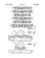
- a passivation layer 24 and an interconnect system 31 that includes or contains a metal layer 23, an under bump metallurgy 25, and an interconnect bump 29 in FIG. 2will be described in detail below.
- FIG. 2portrays electrically conductive layer or metal layer 23 over substrate 21.
- Metal layer 23represents a portion of the metallization pattern of step 12.
- Metal layer 23is electrically coupled to integrated circuit 22.
- Metal layer 23preferably comprises aluminum but can also contain copper and silicon as known in the art.
- Metal layer 23is formed or fabricated over substrate 21 using, for example, conventional sputtering, photolithographic, and etching processes. In a preferred embodiment, metal layer 23 is a metal pad having a diameter of approximately 75-100 microns and a thickness of approximately 1-3 microns.
- step 13provides a passivation layer over the metallization pattern.
- passivation layer 24is located over metal layer 23, integrated circuit 22, and substrate 21.
- Passivation layer 24can be deposited over substrate 21 using, for example, a chemical vapor deposition technique.
- passivation layer 24comprises silicon oxide, silicon nitride, or silicon oxynitride and is approximately 0.3-1.0 microns thick.
- passivation layer 24is deposited over substrate 21, a portion of passivation layer 24 is removed using an etch process. Specifically, a portion of passivation layer 24 located over metal layer 23 is removed.
- a photolithographic etch mask(not shown) can be used to define the desired portion of passivation layer 24 to be removed by the etch process. The photolithographic etch mask is removed from passivation layer 24 after etching passivation layer 24.
- step 14the under bump metallurgy of step 14 is represented by under bump metallurgy or UBM 25.
- UBM 25is located over substrate 21, integrated circuit 22, metal layer 23, and passivation layer 24.
- UBM 25comprises three layers: a barrier layer or layer 26, a mixture layer or layer 27, and an adhesion layer or layer 28.
- a barrier layer or layer 26comprises a barrier material including, but not limited to, titanium tungsten, nickel, or chrome but preferably comprises titanium and is preferably approximately 1,000-1,500 angstroms ( ⁇ ) thick.
- Layer 28comprises an adhesion material including, but not limited to, copper and is preferably approximately 4,000-6,000 ⁇ thick.
- Layer 27, which is located between layers 26 and 28,contains the barrier material of layer 26 and the adhesion material of layer 28.
- layer 27comprises titanium copper and is approximately 1,000-2,000 ⁇ thick.
- layers 26, 27, and 28can be evaporated over substrate 21, layers 26, 27, and 28 are preferably sputtered over substrate 21.
- a sputtering techniqueis preferred because it is faster than an evaporation technique and because it provides better adhesion for the deposited layers.
- a titanium sputtering targetis used for sputtering layer 26
- a copper sputtering targetis used for sputtering layer 28
- a third sputtering targetcomprised of approximately 50 percent (%) titanium and 50% copper is used for sputtering layer 27.
- the Materials Research Corporation of Orangeburg, N.Y.manufactures a sputtering tool having a model number 643 that can hold three sputtering targets.
- both the titanium sputtering target and the copper sputtering targetare used for sputtering layer 27. In other words, instead of using a single sputtering target, two separate sputtering targets can be used to deposit layer 27.
- step 15provides an interconnect bump over the under bump metallurgy.
- interconnect bump 29is located over UBM 25, metal layer 23, and substrate 21.
- Interconnect bump 29is electrically coupled to integrated circuit 22 through UBM 25 and metal layer 23.
- interconnect bumpis comprised of solder, which is electroplated over UBM 25.
- a photolithographic pattern(not shown) is formed over UBM 25 and exposes a portion of UBM 25, and an electroplating process is used to form interconnect bump 29 over the exposed portion of UBM 25.
- interconnect bump 29is a solder comprised of approximately 97%-5% lead and 3%-95% tin. In an alternative embodiment, the solder contains indium or bismuth in place of the lead. In a preferred embodiment, interconnect bump 29 is similar in shape to a sphere with a diameter of approximately 50-100 microns. Preferably, interconnect bump 29 has a smaller diameter than metal layer 23.
- UBM 25 and specifically layer 28serves as a plating bus.
- subsequent processingsuch as, for example, reflow during bump formation, die assembly, or rework, a portion of the copper in layer 28 is consumed by interconnect bump 29.
- interconnect bump 29At high temperatures over about 150-350 degrees Celsius (°C.), an intermetallic of tin and copper can be formed at the interface between layer 28 and interconnect bump 29.
- Copperis preferably used in layers 27 and 28 because solder adheres to copper.
- Titaniumis preferably used in layer 26 because titanium is a diffusion barrier for copper and solder. The titanium in layer 26 prevents contaminants such as, for example, the copper of layers 27 and 28 and the lead and tin of interconnect bump 29 from diffusing into metal layer 23. Titanium is also preferably used in layer 26 because titanium provides a low stress adhesion layer to the aluminum of metal layer 23.
- layer 27is located over layer 26 to provide a transition layer or region between the barrier material of layer 26 and interconnect bump 29. If the copper of layer 28 is completely consumed by the solder of interconnect bump 29, layer 27 also serves as a wettable adhesion film for the solder of interconnect bump 29. Interconnect bump 29 will not completely consume layer 27 because of the titanium in layer 27.
- step 16which etches the under bump metallurgy while using the interconnect bump as an etch mask for the under bump metallurgy.
- FIG. 2portrays semiconductor component 20 and interconnect system 31 prior to step 16, which removes or etches portion 30 of UBM 25.
- FIG. 3portrays semiconductor component 20 and interconnect system 31 after the etch process of step 16.
- interconnect bump 29is comprised of lead and tin and where layer 28 is comprised of copper
- an etchantthat is commercially available under the name MetexTM from MacDermid, Incorporated of Waterbury, Conn. is used to wet etch layer 28 at room temperature for about 2-3 minutes.
- Interconnect bump 29serves as an etch mask for layer 28 when the MetexTM etchant is used in step 16.
- a different etchantis preferably used to remove layers 27 and 26.
- a solutioncomprised of about 100-300 milliliters (ml) of 30% hydrogen peroxide (H 2 0 2 ), about 100-300 ml of deionized water (H 2 0), about 1-40 ml of ammonium hydroxide (NH 4 0H), and about 1-50 grams of (ethylenedinitrilo) tetraacetic acid tetrasodium salt, dihydrate is used to etch layers 27 and 26 at about 15°-30°C. for approximately 2-5 minutes.
- the pH level of the above etchantis between approximately 6-14.
- the volumetric ratio between the 30% hydrogen peroxide and the deionized wateris approximately 1:1. It is understood that the amount of 30% hydrogen peroxide in the wet etchant described above is limited by the fact that high concentrations of hydrogen peroxide can etch the lead in interconnect bump 29.
- interconnect bump 29serves as an etch mask for layers 27 and 26 when this second wet etchant is used in step 16 of method 10.
- the second wet etchantalso selectively etches layers 26 and 27 versus layer 28 and interconnect bump 29.
- the (ethylenedinitrilo) tetraacetic acid tetrasodium salt, dihydrate in the above etchantcan be replaced with (ethylenedinitrilo) tetraacetic acid disodium salt, dihydrate.
- interconnect bump 29is not substantially etched by the etchants of step 16, and therefore, interconnect bump 29 is used as the etch mask for step 16.
- the cycle time, complexity, and cost of the present inventionis reduced compared to the cycle time, complexity, and cost of the prior art because an extra masking step is not needed in the present invention.
- substrate 21is comprised of a material other than a semiconductor.
- substrate 21can be a polyester circuit board.
- an electroless plating processcan be used in place of the electroplating process of step 15 in method 10.
- Yet another alternative embodimentuses a polyimide layer over passivation layer 24 or in place of passivation layer 24.
- the present inventioneliminates problems associated with poor reliability due to a lack of adhesion between interconnect bumps and under bump metallurgy.
- the present inventionalso eliminates the need to plate a thick copper layer over the under bump metallurgy to ensure adhesion between the interconnect bump and the UBM.
- the present inventionalso reduces the cycle time, cost, and complexity of the process for manufacturing an interconnect system.
Landscapes
- Engineering & Computer Science (AREA)
- Computer Hardware Design (AREA)
- Microelectronics & Electronic Packaging (AREA)
- Power Engineering (AREA)
- Manufacturing & Machinery (AREA)
- Internal Circuitry In Semiconductor Integrated Circuit Devices (AREA)
Abstract
Description
Claims (11)
Priority Applications (2)
| Application Number | Priority Date | Filing Date | Title |
|---|---|---|---|
| US08/578,255US5773359A (en) | 1995-12-26 | 1995-12-26 | Interconnect system and method of fabrication |
| JP8353600AJPH09186163A (en) | 1995-12-26 | 1996-12-17 | Interconnecting system and manufacture thereof |
Applications Claiming Priority (1)
| Application Number | Priority Date | Filing Date | Title |
|---|---|---|---|
| US08/578,255US5773359A (en) | 1995-12-26 | 1995-12-26 | Interconnect system and method of fabrication |
Publications (1)
| Publication Number | Publication Date |
|---|---|
| US5773359Atrue US5773359A (en) | 1998-06-30 |
Family
ID=24312069
Family Applications (1)
| Application Number | Title | Priority Date | Filing Date |
|---|---|---|---|
| US08/578,255Expired - LifetimeUS5773359A (en) | 1995-12-26 | 1995-12-26 | Interconnect system and method of fabrication |
Country Status (2)
| Country | Link |
|---|---|
| US (1) | US5773359A (en) |
| JP (1) | JPH09186163A (en) |
Cited By (93)
| Publication number | Priority date | Publication date | Assignee | Title |
|---|---|---|---|---|
| US5885891A (en)* | 1996-07-17 | 1999-03-23 | Kabushiki Kaisha Toshiba | Method of manufacturing semiconductor device |
| US6028011A (en)* | 1997-10-13 | 2000-02-22 | Matsushita Electric Industrial Co., Ltd. | Method of forming electric pad of semiconductor device and method of forming solder bump |
| US6073829A (en)* | 1997-02-27 | 2000-06-13 | Nokia Mobile Phones Limited | Method and arrangement for attaching a component |
| US6077775A (en)* | 1998-08-20 | 2000-06-20 | The United States Of America As Represented By The Secretary Of The Navy | Process for making a semiconductor device with barrier film formation using a metal halide and products thereof |
| US6083818A (en)* | 1998-08-20 | 2000-07-04 | The United States Of America As Represented By The Secretary Of The Navy | Electronic devices with strontium barrier film and process for making same |
| US6130141A (en)* | 1998-10-14 | 2000-10-10 | Lucent Technologies Inc. | Flip chip metallization |
| US6153503A (en)* | 1997-03-10 | 2000-11-28 | National Science Council | Continuous process for producing solder bumps on electrodes of semiconductor chips |
| US6162652A (en)* | 1997-12-31 | 2000-12-19 | Intel Corporation | Process for sort testing C4 bumped wafers |
| US6171953B1 (en) | 1998-08-20 | 2001-01-09 | The United States Of America As Represented By The Secretary Of The Navy | Processes for making electronic devices with rubidum barrier film |
| US6251797B1 (en)* | 1999-02-26 | 2001-06-26 | Rohm Co., Ltd. | Method of fabricating semiconductor device |
| US6258705B1 (en) | 2000-08-21 | 2001-07-10 | Siliconeware Precision Industries Co., Ltd. | Method of forming circuit probing contact points on fine pitch peripheral bond pads on flip chip |
| US6291876B1 (en) | 1998-08-20 | 2001-09-18 | The United States Of America As Represented By The Secretary Of The Navy | Electronic devices with composite atomic barrier film and process for making same |
| KR100311975B1 (en)* | 1999-12-16 | 2001-10-17 | 윤종용 | semiconductor device and method for manufacturing the same |
| WO2001017013A3 (en)* | 1999-09-02 | 2001-10-25 | Intel Corp | A method and an apparatus for forming an under bump metallization structure |
| US6327158B1 (en)* | 1999-01-15 | 2001-12-04 | National Semiconductor Corporation | Metal pads for electrical probe testing on wafer with bump interconnects |
| US6329608B1 (en) | 1995-04-05 | 2001-12-11 | Unitive International Limited | Key-shaped solder bumps and under bump metallurgy |
| US6332988B1 (en)* | 1999-06-02 | 2001-12-25 | International Business Machines Corporation | Rework process |
| US6351036B1 (en) | 1998-08-20 | 2002-02-26 | The United States Of America As Represented By The Secretary Of The Navy | Electronic devices with a barrier film and process for making same |
| US20020025675A1 (en)* | 2000-05-03 | 2002-02-28 | Chu Tak Kin | Electronic devices with diffusion barrier and process for making same |
| US6372624B1 (en)* | 1997-08-04 | 2002-04-16 | Micron Technology, Inc. | Method for fabricating solder bumps by wave soldering |
| US6388203B1 (en) | 1995-04-04 | 2002-05-14 | Unitive International Limited | Controlled-shaped solder reservoirs for increasing the volume of solder bumps, and structures formed thereby |
| US6387793B1 (en)* | 2000-03-09 | 2002-05-14 | Hrl Laboratories, Llc | Method for manufacturing precision electroplated solder bumps |
| US6413878B1 (en) | 1998-07-30 | 2002-07-02 | Motorola, Inc. | Method of manufacturing electronic components |
| US6423625B1 (en)* | 1999-08-30 | 2002-07-23 | Taiwan Semiconductor Manufacturing Company Ltd. | Method of improving the bondability between Au wires and Cu bonding pads |
| US6462415B1 (en)* | 2000-01-11 | 2002-10-08 | Fujitsu Limited | Semiconductor device as an object of thickness reduction |
| US6475896B1 (en)* | 1996-12-04 | 2002-11-05 | Seiko Epson Corporation | Electronic component and semiconductor device, method of making the same and method of mounting the same, circuit board, and electronic instrument |
| US20030094693A1 (en)* | 2001-11-20 | 2003-05-22 | Jen-Kuang Fang | Multi-chip module packaging device |
| US20030107023A1 (en)* | 2001-12-06 | 2003-06-12 | Lg.Philips Lcd Co., Ltd. | Etchant for etching metal wiring layers and method for forming thin film transistor by using the same |
| DE10157209A1 (en)* | 2001-11-22 | 2003-06-12 | Fraunhofer Ges Forschung | Contact bump formation by electroless deposition uses resist which is structured to define deposition surfaces and penetrating, confining sidewalls |
| US6596619B1 (en)* | 2002-05-17 | 2003-07-22 | Taiwan Semiconductor Manufacturing Company | Method for fabricating an under bump metallization structure |
| US6649533B1 (en) | 1999-05-05 | 2003-11-18 | Advanced Micro Devices, Inc. | Method and apparatus for forming an under bump metallurgy layer |
| US6692629B1 (en) | 2000-09-07 | 2004-02-17 | Siliconware Precision Industries Co., Ltd. | Flip-chip bumbing method for fabricating solder bumps on semiconductor wafer |
| US6720654B2 (en) | 1998-08-20 | 2004-04-13 | The United States Of America As Represented By The Secretary Of The Navy | Electronic devices with cesium barrier film and process for making same |
| US6734558B2 (en) | 1998-08-20 | 2004-05-11 | The United States Of America As Represented By The Secretary Of The Navy | Electronic devices with barium barrier film and process for making same |
| US20040092092A1 (en)* | 2002-11-12 | 2004-05-13 | Siliconware Precision Industries, Ltd. | Semiconductor device with under bump metallurgy and method for fabricating the same |
| US6740427B2 (en)* | 2001-09-21 | 2004-05-25 | Intel Corporation | Thermo-mechanically robust C4 ball-limiting metallurgy to prevent failure due to die-package interaction and method of making same |
| EP1280101A4 (en)* | 2000-04-04 | 2004-06-16 | Toray Eng Co Ltd | COF HOUSING PRODUCTION PROCESS |
| US6762503B2 (en)* | 2002-08-29 | 2004-07-13 | Micron Technology, Inc. | Innovative solder ball pad structure to ease design rule, methods of fabricating same and substrates, electronic device assemblies and systems employing same |
| US20040159944A1 (en)* | 2001-09-21 | 2004-08-19 | Madhav Datta | Copper-containing C4 ball-limiting metallurgy stack for enhanced reliability of packaged structures and method of making same |
| US6806578B2 (en) | 2000-03-16 | 2004-10-19 | International Business Machines Corporation | Copper pad structure |
| US20040209406A1 (en)* | 2003-02-18 | 2004-10-21 | Jong-Rong Jan | Methods of selectively bumping integrated circuit substrates and related structures |
| US20040229458A1 (en)* | 2003-05-13 | 2004-11-18 | Stmicroelectronics Inc. | Method and structure of a thick metal layer using multiple deposition chambers |
| US6879027B2 (en)* | 2000-11-30 | 2005-04-12 | Kabushiki Kaisha Shinkawa | Semiconductor device having bumps |
| US20050085062A1 (en)* | 2003-10-15 | 2005-04-21 | Semitool, Inc. | Processes and tools for forming lead-free alloy solder precursors |
| US20050136641A1 (en)* | 2003-10-14 | 2005-06-23 | Rinne Glenn A. | Solder structures for out of plane connections and related methods |
| US6960828B2 (en) | 2002-06-25 | 2005-11-01 | Unitive International Limited | Electronic structures including conductive shunt layers |
| US20050279809A1 (en)* | 2000-11-10 | 2005-12-22 | Rinne Glenn A | Optical structures including liquid bumps and related methods |
| US20060023107A1 (en)* | 2004-08-02 | 2006-02-02 | Bolken Todd O | Microelectronic imagers with optics supports having threadless interfaces and methods for manufacturing such microelectronic imagers |
| US20060030139A1 (en)* | 2002-06-25 | 2006-02-09 | Mis J D | Methods of forming lead free solder bumps and related structures |
| US20060076679A1 (en)* | 2002-06-25 | 2006-04-13 | Batchelor William E | Non-circular via holes for bumping pads and related structures |
| US7045389B1 (en)* | 1996-08-27 | 2006-05-16 | Nippon Steel Corporation | Method for fabricating a semiconductor devices provided with low melting point metal bumps |
| US20060151880A1 (en)* | 2005-01-10 | 2006-07-13 | Micron Technology, Inc. | Interconnect structures with bond-pads and methods of forming bump sites on bond-pads |
| US20060199363A1 (en)* | 2004-06-29 | 2006-09-07 | Micron Technology, Inc. | Microelectronic devices and methods for forming interconnects in microelectronic devices |
| US20060205170A1 (en)* | 2005-03-09 | 2006-09-14 | Rinne Glenn A | Methods of forming self-healing metal-insulator-metal (MIM) structures and related devices |
| US20060240687A1 (en)* | 2004-08-27 | 2006-10-26 | Micron Technology, Inc. | Slanted vias for electrical circuits on circuit boards and other substrates |
| US20060252245A1 (en)* | 2005-05-04 | 2006-11-09 | Chun-Chi Ke | Fabrication method of under bump metallurgy structure |
| US20060290001A1 (en)* | 2005-06-28 | 2006-12-28 | Micron Technology, Inc. | Interconnect vias and associated methods of formation |
| US7156284B2 (en) | 2000-12-15 | 2007-01-02 | Unitive International Limited | Low temperature methods of bonding components and related structures |
| US20070045812A1 (en)* | 2005-08-31 | 2007-03-01 | Micron Technology, Inc. | Microfeature assemblies including interconnect structures and methods for forming such interconnect structures |
| US20070045848A1 (en)* | 2005-08-31 | 2007-03-01 | Advanced Semiconductor Engineering, Inc. | Wafer structure |
| DE102005051330A1 (en)* | 2005-10-25 | 2007-05-03 | Infineon Technologies Ag | Methods of producing and cleaning external contacts for surface-mounted chips and producing such chips tempers galvanically deposited layer followed by rapid thermal processing and moistening |
| US20070120251A1 (en)* | 2002-10-15 | 2007-05-31 | Seiko Epson Corporation | Semiconductor wafer, semiconductor device and method of manufacturing the same, circuit board, and electronic equipment |
| US7253078B1 (en) | 1999-07-22 | 2007-08-07 | National Semiconductor Corporation | Method and apparatus for forming an underfill adhesive layer |
| US20070182004A1 (en)* | 2006-02-08 | 2007-08-09 | Rinne Glenn A | Methods of Forming Electronic Interconnections Including Compliant Dielectric Layers and Related Devices |
| US7282375B1 (en) | 2004-04-14 | 2007-10-16 | National Semiconductor Corporation | Wafer level package design that facilitates trimming and testing |
| US20070256761A1 (en)* | 2006-05-08 | 2007-11-08 | Indium Corporation Of America | Alloy compositions and techniques for reducing intermetallic compound thickness and oxidation of metals and alloys |
| US7301222B1 (en) | 2003-02-12 | 2007-11-27 | National Semiconductor Corporation | Apparatus for forming a pre-applied underfill adhesive layer for semiconductor wafer level chip-scale packages |
| US7413979B2 (en) | 2003-11-13 | 2008-08-19 | Micron Technology, Inc. | Methods for forming vias in microelectronic devices, and methods for packaging microelectronic devices |
| US20080210301A1 (en)* | 2003-04-10 | 2008-09-04 | Sunpower Corporation | Metal contact structure for solar cell and method of manufacture |
| US7423337B1 (en) | 2002-08-19 | 2008-09-09 | National Semiconductor Corporation | Integrated circuit device package having a support coating for improved reliability during temperature cycling |
| US7425499B2 (en) | 2004-08-24 | 2008-09-16 | Micron Technology, Inc. | Methods for forming interconnects in vias and microelectronic workpieces including such interconnects |
| US20080308931A1 (en)* | 2004-03-10 | 2008-12-18 | Unitive International Limited | Electronic Structures Including Barrier Layers Defining Lips |
| US20080318353A1 (en)* | 2004-08-24 | 2008-12-25 | Oliver Steven D | Microelectronic imagers with optical devices having integral reference features and methods for manufacturing such microelectronic imagers |
| US20090008780A1 (en)* | 2004-12-30 | 2009-01-08 | Micron Technology, Inc. | Methods for forming interconnects in microelectronic workpieces and microelectronic workpieces formed using such methods |
| US7622377B2 (en) | 2005-09-01 | 2009-11-24 | Micron Technology, Inc. | Microfeature workpiece substrates having through-substrate vias, and associated methods of formation |
| US7629249B2 (en) | 2006-08-28 | 2009-12-08 | Micron Technology, Inc. | Microfeature workpieces having conductive interconnect structures formed by chemically reactive processes, and associated systems and methods |
| US7674701B2 (en) | 2006-02-08 | 2010-03-09 | Amkor Technology, Inc. | Methods of forming metal layers using multi-layer lift-off patterns |
| US7683458B2 (en) | 2004-09-02 | 2010-03-23 | Micron Technology, Inc. | Through-wafer interconnects for photoimager and memory wafers |
| US7749899B2 (en) | 2006-06-01 | 2010-07-06 | Micron Technology, Inc. | Microelectronic workpieces and methods and systems for forming interconnects in microelectronic workpieces |
| US7830018B2 (en) | 2007-08-31 | 2010-11-09 | Micron Technology, Inc. | Partitioned through-layer via and associated systems and methods |
| US7863187B2 (en) | 2005-09-01 | 2011-01-04 | Micron Technology, Inc. | Microfeature workpieces and methods for forming interconnects in microfeature workpieces |
| US7884015B2 (en) | 2007-12-06 | 2011-02-08 | Micron Technology, Inc. | Methods for forming interconnects in microelectronic workpieces and microelectronic workpieces formed using such methods |
| US7902643B2 (en) | 2006-08-31 | 2011-03-08 | Micron Technology, Inc. | Microfeature workpieces having interconnects and conductive backplanes, and associated systems and methods |
| US8008192B2 (en) | 2005-06-28 | 2011-08-30 | Micron Technology, Inc. | Conductive interconnect structures and formation methods using supercritical fluids |
| US20110248406A1 (en)* | 2010-04-09 | 2011-10-13 | Renesas Electronics Corporation | Method of Manufacturing Semiconductor Device |
| US8084866B2 (en) | 2003-12-10 | 2011-12-27 | Micron Technology, Inc. | Microelectronic devices and methods for filling vias in microelectronic devices |
| US20130037603A1 (en)* | 2010-02-10 | 2013-02-14 | Agency For Science ,Technology And Research | Method of Forming a Bonded Structure |
| US8536485B2 (en) | 2004-05-05 | 2013-09-17 | Micron Technology, Inc. | Systems and methods for forming apertures in microfeature workpieces |
| USRE46147E1 (en)* | 1998-05-22 | 2016-09-13 | Sony Corporation | Semiconductor device and method of fabricating the same |
| DE112006000505B4 (en)* | 2005-03-04 | 2017-07-20 | International Rectifier Corp. | Semiconductor device manufacturing |
| CN113540017A (en)* | 2021-06-30 | 2021-10-22 | 佛山市国星光电股份有限公司 | IGBT module packaging structure and manufacturing method thereof |
| US11164830B2 (en)* | 2015-01-14 | 2021-11-02 | Infineon Technologies Ag | Semiconductor chip and method of processing a semiconductor chip |
| US11343916B2 (en)* | 2019-12-12 | 2022-05-24 | AT&S(China) Co. Ltd. | Component carrier and method of manufacturing the same |
Families Citing this family (4)
| Publication number | Priority date | Publication date | Assignee | Title |
|---|---|---|---|---|
| KR100732648B1 (en) | 2000-02-22 | 2007-06-28 | 도레이엔지니어링가부시키가이샤 | Contactless ID card and its manufacturing method |
| JP2006156910A (en)* | 2004-12-01 | 2006-06-15 | Denso Corp | Semiconductor device |
| JP6024079B2 (en)* | 2011-08-18 | 2016-11-09 | 富士通株式会社 | Semiconductor device, method for manufacturing the same, and electronic device |
| JP2019066453A (en)* | 2017-09-29 | 2019-04-25 | ミネベアミツミ株式会社 | Strain gauge |
Citations (10)
| Publication number | Priority date | Publication date | Assignee | Title |
|---|---|---|---|---|
| JPS57154858A (en)* | 1981-03-20 | 1982-09-24 | Hitachi Ltd | Method for formation of electrode |
| JPS61251153A (en)* | 1985-04-30 | 1986-11-08 | Fujitsu Ltd | Bump formation method for semiconductor devices |
| JPH02253628A (en)* | 1989-03-28 | 1990-10-12 | Nec Corp | Manufacture of semiconductor device |
| JPH04133330A (en)* | 1990-09-25 | 1992-05-07 | Toshiba Corp | Semiconductor device and its connection method |
| JPH0513421A (en)* | 1991-07-04 | 1993-01-22 | Tanaka Kikinzoku Kogyo Kk | Bump forming method |
| US5298459A (en)* | 1988-11-21 | 1994-03-29 | Seiko Epson Corporation | Method of manufacturing semiconductor device terminal having a gold bump electrode |
| US5310699A (en)* | 1984-08-28 | 1994-05-10 | Sharp Kabushiki Kaisha | Method of manufacturing a bump electrode |
| US5447599A (en)* | 1991-11-12 | 1995-09-05 | Cornell Research Foundation, Inc. | Self-aligned process for capping copper lines |
| US5470787A (en)* | 1994-05-02 | 1995-11-28 | Motorola, Inc. | Semiconductor device solder bump having intrinsic potential for forming an extended eutectic region and method for making and using the same |
| US5587336A (en)* | 1994-12-09 | 1996-12-24 | Vlsi Technology | Bump formation on yielded semiconductor dies |
- 1995
- 1995-12-26USUS08/578,255patent/US5773359A/ennot_activeExpired - Lifetime
- 1996
- 1996-12-17JPJP8353600Apatent/JPH09186163A/enactivePending
Patent Citations (10)
| Publication number | Priority date | Publication date | Assignee | Title |
|---|---|---|---|---|
| JPS57154858A (en)* | 1981-03-20 | 1982-09-24 | Hitachi Ltd | Method for formation of electrode |
| US5310699A (en)* | 1984-08-28 | 1994-05-10 | Sharp Kabushiki Kaisha | Method of manufacturing a bump electrode |
| JPS61251153A (en)* | 1985-04-30 | 1986-11-08 | Fujitsu Ltd | Bump formation method for semiconductor devices |
| US5298459A (en)* | 1988-11-21 | 1994-03-29 | Seiko Epson Corporation | Method of manufacturing semiconductor device terminal having a gold bump electrode |
| JPH02253628A (en)* | 1989-03-28 | 1990-10-12 | Nec Corp | Manufacture of semiconductor device |
| JPH04133330A (en)* | 1990-09-25 | 1992-05-07 | Toshiba Corp | Semiconductor device and its connection method |
| JPH0513421A (en)* | 1991-07-04 | 1993-01-22 | Tanaka Kikinzoku Kogyo Kk | Bump forming method |
| US5447599A (en)* | 1991-11-12 | 1995-09-05 | Cornell Research Foundation, Inc. | Self-aligned process for capping copper lines |
| US5470787A (en)* | 1994-05-02 | 1995-11-28 | Motorola, Inc. | Semiconductor device solder bump having intrinsic potential for forming an extended eutectic region and method for making and using the same |
| US5587336A (en)* | 1994-12-09 | 1996-12-24 | Vlsi Technology | Bump formation on yielded semiconductor dies |
Cited By (219)
| Publication number | Priority date | Publication date | Assignee | Title |
|---|---|---|---|---|
| US6392163B1 (en) | 1995-04-04 | 2002-05-21 | Unitive International Limited | Controlled-shaped solder reservoirs for increasing the volume of solder bumps |
| US6388203B1 (en) | 1995-04-04 | 2002-05-14 | Unitive International Limited | Controlled-shaped solder reservoirs for increasing the volume of solder bumps, and structures formed thereby |
| US6329608B1 (en) | 1995-04-05 | 2001-12-11 | Unitive International Limited | Key-shaped solder bumps and under bump metallurgy |
| US6389691B1 (en)* | 1995-04-05 | 2002-05-21 | Unitive International Limited | Methods for forming integrated redistribution routing conductors and solder bumps |
| US5885891A (en)* | 1996-07-17 | 1999-03-23 | Kabushiki Kaisha Toshiba | Method of manufacturing semiconductor device |
| US7045389B1 (en)* | 1996-08-27 | 2006-05-16 | Nippon Steel Corporation | Method for fabricating a semiconductor devices provided with low melting point metal bumps |
| US20090181521A1 (en)* | 1996-12-04 | 2009-07-16 | Seiko Epson Corporation | Electronic component and semiconductor device, method of making the same and method of mounting the same, circuit board, and electronic instrument |
| US20100273311A1 (en)* | 1996-12-04 | 2010-10-28 | Seiko Epson Corporation | Electronic component and semiconductor device, method of making the same and method of mounting the same, circuit board, and electronic instrument |
| US7888260B2 (en) | 1996-12-04 | 2011-02-15 | Seiko Epson Corporation | Method of making electronic device |
| US8115284B2 (en)* | 1996-12-04 | 2012-02-14 | Seiko Epson Corporation | Electronic component and semiconductor device, method of making the same and method of mounting the same, circuit board and electronic instrument |
| US20110095432A1 (en)* | 1996-12-04 | 2011-04-28 | Seiko Epson Corporation | Electronic component and semiconductor device, method of making the same and method of mounting the same, circuit board and electronic instrument |
| US6475896B1 (en)* | 1996-12-04 | 2002-11-05 | Seiko Epson Corporation | Electronic component and semiconductor device, method of making the same and method of mounting the same, circuit board, and electronic instrument |
| US20060131705A1 (en)* | 1996-12-04 | 2006-06-22 | Seiko Epson Corporation | Electronic component and semiconductor device, method of making the same and method of mounting the same, circuit board, and electronic instrument |
| US20060097369A1 (en)* | 1996-12-04 | 2006-05-11 | Seiko Epson Corporation | Electronic component and semiconductor device, method of making the same and method of mounting the same, circuit board, and electronic instrument |
| US7842598B2 (en) | 1996-12-04 | 2010-11-30 | Seiko Epson Corporation | Electronic component and semiconductor device, method of making the same and method of mounting the same, circuit board, and electronic instrument |
| US6730589B2 (en) | 1996-12-04 | 2004-05-04 | Seiko Epson Corporation | Electronic component and semiconductor device, method of making the same and method of mounting the same, circuit board, and electronic instrument |
| US7049686B2 (en) | 1996-12-04 | 2006-05-23 | Seiko Epson Corporation | Electronic component and semiconductor device, method of making the same and method of mounting the same, circuit board, and electronic instrument |
| US7470979B2 (en) | 1996-12-04 | 2008-12-30 | Seiko Epson Corporation | Electronic component and semiconductor device, method of making the same and method of mounting the same, circuit board, and electronic instrument |
| US7511362B2 (en) | 1996-12-04 | 2009-03-31 | Seiko Epson Corporation | Electronic component and semiconductor device, method of making the same and method of mounting the same, circuit board, and electronic instrument |
| US20040180486A1 (en)* | 1996-12-04 | 2004-09-16 | Seiko Epson Corporation | Electronic component and semiconductor device, method of making the same and method of mounting the same, circuit board, and electronic instrument |
| US6073829A (en)* | 1997-02-27 | 2000-06-13 | Nokia Mobile Phones Limited | Method and arrangement for attaching a component |
| US6153503A (en)* | 1997-03-10 | 2000-11-28 | National Science Council | Continuous process for producing solder bumps on electrodes of semiconductor chips |
| US6637638B1 (en) | 1997-08-04 | 2003-10-28 | Micron Technology, Inc. | System for fabricating solder bumps on semiconductor components |
| US6372624B1 (en)* | 1997-08-04 | 2002-04-16 | Micron Technology, Inc. | Method for fabricating solder bumps by wave soldering |
| US6028011A (en)* | 1997-10-13 | 2000-02-22 | Matsushita Electric Industrial Co., Ltd. | Method of forming electric pad of semiconductor device and method of forming solder bump |
| US6162652A (en)* | 1997-12-31 | 2000-12-19 | Intel Corporation | Process for sort testing C4 bumped wafers |
| USRE46147E1 (en)* | 1998-05-22 | 2016-09-13 | Sony Corporation | Semiconductor device and method of fabricating the same |
| US6413878B1 (en) | 1998-07-30 | 2002-07-02 | Motorola, Inc. | Method of manufacturing electronic components |
| US6436300B2 (en)* | 1998-07-30 | 2002-08-20 | Motorola, Inc. | Method of manufacturing electronic components |
| US6720654B2 (en) | 1998-08-20 | 2004-04-13 | The United States Of America As Represented By The Secretary Of The Navy | Electronic devices with cesium barrier film and process for making same |
| US6144050A (en)* | 1998-08-20 | 2000-11-07 | The United States Of America As Represented By The Secretary Of The Navy | Electronic devices with strontium barrier film and process for making same |
| US6171953B1 (en) | 1998-08-20 | 2001-01-09 | The United States Of America As Represented By The Secretary Of The Navy | Processes for making electronic devices with rubidum barrier film |
| US6077775A (en)* | 1998-08-20 | 2000-06-20 | The United States Of America As Represented By The Secretary Of The Navy | Process for making a semiconductor device with barrier film formation using a metal halide and products thereof |
| US6188134B1 (en) | 1998-08-20 | 2001-02-13 | The United States Of America As Represented By The Secretary Of The Navy | Electronic devices with rubidium barrier film and process for making same |
| US6083818A (en)* | 1998-08-20 | 2000-07-04 | The United States Of America As Represented By The Secretary Of The Navy | Electronic devices with strontium barrier film and process for making same |
| US6291876B1 (en) | 1998-08-20 | 2001-09-18 | The United States Of America As Represented By The Secretary Of The Navy | Electronic devices with composite atomic barrier film and process for making same |
| US6566247B2 (en) | 1998-08-20 | 2003-05-20 | The United States Of America As Represented By The Secretary Of The Navy | Electronic devices with composite atomic barrier film and process for making same |
| US6734558B2 (en) | 1998-08-20 | 2004-05-11 | The United States Of America As Represented By The Secretary Of The Navy | Electronic devices with barium barrier film and process for making same |
| US6351036B1 (en) | 1998-08-20 | 2002-02-26 | The United States Of America As Represented By The Secretary Of The Navy | Electronic devices with a barrier film and process for making same |
| US6130141A (en)* | 1998-10-14 | 2000-10-10 | Lucent Technologies Inc. | Flip chip metallization |
| US6327158B1 (en)* | 1999-01-15 | 2001-12-04 | National Semiconductor Corporation | Metal pads for electrical probe testing on wafer with bump interconnects |
| US6251797B1 (en)* | 1999-02-26 | 2001-06-26 | Rohm Co., Ltd. | Method of fabricating semiconductor device |
| US6649533B1 (en) | 1999-05-05 | 2003-11-18 | Advanced Micro Devices, Inc. | Method and apparatus for forming an under bump metallurgy layer |
| US6332988B1 (en)* | 1999-06-02 | 2001-12-25 | International Business Machines Corporation | Rework process |
| US7253078B1 (en) | 1999-07-22 | 2007-08-07 | National Semiconductor Corporation | Method and apparatus for forming an underfill adhesive layer |
| US6423625B1 (en)* | 1999-08-30 | 2002-07-23 | Taiwan Semiconductor Manufacturing Company Ltd. | Method of improving the bondability between Au wires and Cu bonding pads |
| GB2370417A (en)* | 1999-09-02 | 2002-06-26 | Intel Corp | A method and apparatus for forming an under bump metallization structure |
| GB2370417B (en)* | 1999-09-02 | 2004-03-31 | Intel Corp | A method and apparatus for forming an under bump metallization structure |
| US6312830B1 (en) | 1999-09-02 | 2001-11-06 | Intel Corporation | Method and an apparatus for forming an under bump metallization structure |
| WO2001017013A3 (en)* | 1999-09-02 | 2001-10-25 | Intel Corp | A method and an apparatus for forming an under bump metallization structure |
| US6461954B1 (en) | 1999-09-02 | 2002-10-08 | Intel Corporation | Method and an apparatus for forming an under bump metallization structure |
| US6486053B2 (en)* | 1999-12-16 | 2002-11-26 | Samsung Electronics Co., Ltd. | Semiconductor device and fabricating method therefor |
| KR100311975B1 (en)* | 1999-12-16 | 2001-10-17 | 윤종용 | semiconductor device and method for manufacturing the same |
| US6348730B1 (en)* | 1999-12-16 | 2002-02-19 | Samsung Electronics Co., Ltd. | Semiconductor device and fabricating method therefor |
| US6462415B1 (en)* | 2000-01-11 | 2002-10-08 | Fujitsu Limited | Semiconductor device as an object of thickness reduction |
| US6387793B1 (en)* | 2000-03-09 | 2002-05-14 | Hrl Laboratories, Llc | Method for manufacturing precision electroplated solder bumps |
| US6828677B2 (en) | 2000-03-09 | 2004-12-07 | Hrl Laboratories, Llc. | Precision electroplated solder bumps and method for manufacturing thereof |
| US6806578B2 (en) | 2000-03-16 | 2004-10-19 | International Business Machines Corporation | Copper pad structure |
| EP1280101A4 (en)* | 2000-04-04 | 2004-06-16 | Toray Eng Co Ltd | COF HOUSING PRODUCTION PROCESS |
| US20020025675A1 (en)* | 2000-05-03 | 2002-02-28 | Chu Tak Kin | Electronic devices with diffusion barrier and process for making same |
| US6881669B2 (en) | 2000-05-03 | 2005-04-19 | The United States Of America As Represented By The Secretary Of The Navy | Process for making electronic devices having a monolayer diffusion barrier |
| US6465887B1 (en) | 2000-05-03 | 2002-10-15 | The United States Of America As Represented By The Secretary Of The Navy | Electronic devices with diffusion barrier and process for making same |
| US6258705B1 (en) | 2000-08-21 | 2001-07-10 | Siliconeware Precision Industries Co., Ltd. | Method of forming circuit probing contact points on fine pitch peripheral bond pads on flip chip |
| US20020031880A1 (en)* | 2000-08-21 | 2002-03-14 | Siliconware Precision Industries Co., Ltd. | Circuit probing contact pad formed on a bond pad in a flip chip package |
| US6753609B2 (en) | 2000-08-21 | 2004-06-22 | Siliconware Precision Industries Co., Ltd. | Circuit probing contact pad formed on a bond pad in a flip chip package |
| US6692629B1 (en) | 2000-09-07 | 2004-02-17 | Siliconware Precision Industries Co., Ltd. | Flip-chip bumbing method for fabricating solder bumps on semiconductor wafer |
| US20050279809A1 (en)* | 2000-11-10 | 2005-12-22 | Rinne Glenn A | Optical structures including liquid bumps and related methods |
| US7213740B2 (en) | 2000-11-10 | 2007-05-08 | Unitive International Limited | Optical structures including liquid bumps and related methods |
| US20070152020A1 (en)* | 2000-11-10 | 2007-07-05 | Unitive International Limited | Optical structures including liquid bumps |
| US6879027B2 (en)* | 2000-11-30 | 2005-04-12 | Kabushiki Kaisha Shinkawa | Semiconductor device having bumps |
| US7156284B2 (en) | 2000-12-15 | 2007-01-02 | Unitive International Limited | Low temperature methods of bonding components and related structures |
| US7250678B2 (en) | 2001-09-21 | 2007-07-31 | Intel Corporation | Copper-containing C4 ball-limiting metallurgy stack for enhanced reliability of packaged structures and method of making same |
| US20040159947A1 (en)* | 2001-09-21 | 2004-08-19 | Madhav Datta | Copper-containing C4 ball-limiting metallurgy stack for enhanced reliability of packaged structures and method of making same |
| US20040159944A1 (en)* | 2001-09-21 | 2004-08-19 | Madhav Datta | Copper-containing C4 ball-limiting metallurgy stack for enhanced reliability of packaged structures and method of making same |
| US7196001B2 (en) | 2001-09-21 | 2007-03-27 | Intel Corporation | Copper-containing C4 ball-limiting metallurgy stack for enhanced reliability of packaged structures and method of making same |
| US20100117229A1 (en)* | 2001-09-21 | 2010-05-13 | Madhav Datta | Copper-containing C4 ball-limiting metallurgy stack for enhanced reliability of packaged structures and method of making same |
| US6853076B2 (en) | 2001-09-21 | 2005-02-08 | Intel Corporation | Copper-containing C4 ball-limiting metallurgy stack for enhanced reliability of packaged structures and method of making same |
| US20060148233A1 (en)* | 2001-09-21 | 2006-07-06 | Madhav Datta | Copper-containing C4 ball-limiting metallurgy stack for enhanced reliability of packaged structures and method of making same |
| US8952550B2 (en) | 2001-09-21 | 2015-02-10 | Intel Corporation | Copper-containing C4 ball-limiting metallurgy stack for enhanced reliability of packaged structures and method of making same |
| US6740427B2 (en)* | 2001-09-21 | 2004-05-25 | Intel Corporation | Thermo-mechanically robust C4 ball-limiting metallurgy to prevent failure due to die-package interaction and method of making same |
| US10037956B2 (en) | 2001-09-21 | 2018-07-31 | Intel Corporation | Copper-containing C4 ball-limiting metallurgy stack for enhanced reliability of packaged structures and method of making same |
| US6933616B2 (en)* | 2001-11-20 | 2005-08-23 | Advanced Semiconductor Engineering, Inc. | Multi-chip module packaging device using flip-chip bonding technology |
| US20030094693A1 (en)* | 2001-11-20 | 2003-05-22 | Jen-Kuang Fang | Multi-chip module packaging device |
| DE10157209A1 (en)* | 2001-11-22 | 2003-06-12 | Fraunhofer Ges Forschung | Contact bump formation by electroless deposition uses resist which is structured to define deposition surfaces and penetrating, confining sidewalls |
| US20060105579A1 (en)* | 2001-12-06 | 2006-05-18 | Chae Gee S | Etchant for etching metal wiring layers and method for forming thin film transistor by using the same |
| US8257609B2 (en) | 2001-12-06 | 2012-09-04 | Lg Display Co., Ltd. | Etchant for etching metal wiring layers and method for forming thin film transistor by using the same |
| US20030107023A1 (en)* | 2001-12-06 | 2003-06-12 | Lg.Philips Lcd Co., Ltd. | Etchant for etching metal wiring layers and method for forming thin film transistor by using the same |
| US7008548B2 (en)* | 2001-12-06 | 2006-03-07 | Lg.Philips Lcd Co., Ltd. | Etchant for etching metal wiring layers and method for forming thin film transistor by using the same |
| US8308963B2 (en) | 2001-12-06 | 2012-11-13 | Lg Display Co., Ltd. | Etchant for etching metal wiring layers and method for forming thin film transistor by using the same |
| US6770958B2 (en)* | 2002-05-17 | 2004-08-03 | Taiwan Semiconductor Manufacturing Company | Under bump metallization structure |
| US6596619B1 (en)* | 2002-05-17 | 2003-07-22 | Taiwan Semiconductor Manufacturing Company | Method for fabricating an under bump metallization structure |
| US7879715B2 (en) | 2002-06-25 | 2011-02-01 | Unitive International Limited | Methods of forming electronic structures including conductive shunt layers and related structures |
| US6960828B2 (en) | 2002-06-25 | 2005-11-01 | Unitive International Limited | Electronic structures including conductive shunt layers |
| US20080026560A1 (en)* | 2002-06-25 | 2008-01-31 | Unitive International Limited | Methods of forming electronic structures including conductive shunt layers and related structures |
| US7297631B2 (en) | 2002-06-25 | 2007-11-20 | Unitive International Limited | Methods of forming electronic structures including conductive shunt layers and related structures |
| US20060009023A1 (en)* | 2002-06-25 | 2006-01-12 | Unitive International Limited | Methods of forming electronic structures including conductive shunt layers and related structures |
| US20060076679A1 (en)* | 2002-06-25 | 2006-04-13 | Batchelor William E | Non-circular via holes for bumping pads and related structures |
| US20060030139A1 (en)* | 2002-06-25 | 2006-02-09 | Mis J D | Methods of forming lead free solder bumps and related structures |
| US7839000B2 (en) | 2002-06-25 | 2010-11-23 | Unitive International Limited | Solder structures including barrier layers with nickel and/or copper |
| US7531898B2 (en) | 2002-06-25 | 2009-05-12 | Unitive International Limited | Non-Circular via holes for bumping pads and related structures |
| US7547623B2 (en) | 2002-06-25 | 2009-06-16 | Unitive International Limited | Methods of forming lead free solder bumps |
| US7423337B1 (en) | 2002-08-19 | 2008-09-09 | National Semiconductor Corporation | Integrated circuit device package having a support coating for improved reliability during temperature cycling |
| US6762503B2 (en)* | 2002-08-29 | 2004-07-13 | Micron Technology, Inc. | Innovative solder ball pad structure to ease design rule, methods of fabricating same and substrates, electronic device assemblies and systems employing same |
| US6940179B2 (en)* | 2002-08-29 | 2005-09-06 | Micron Technology, Inc. | Innovative solder ball pad structure to ease design rule, methods of fabricating same and substrates, electronic device assemblies and systems employing same |
| US20040173915A1 (en)* | 2002-08-29 | 2004-09-09 | Lee Teck Kheng | Innovative solder ball pad structure to ease design rule, methods of fabricating same and substrates, electronic device assemblies and systems employing same |
| US20070120251A1 (en)* | 2002-10-15 | 2007-05-31 | Seiko Epson Corporation | Semiconductor wafer, semiconductor device and method of manufacturing the same, circuit board, and electronic equipment |
| US7294933B2 (en)* | 2002-10-15 | 2007-11-13 | Seiko Epson Corporation | Semiconductor wafer, semiconductor device and method of manufacturing the same, circuit board, and electronic equipment |
| US20050001313A1 (en)* | 2002-11-12 | 2005-01-06 | Siliconware Precision Industries Co., Ltd. | Semiconductor device with under bump metallurgy and method for fabricating the same |
| US6787903B2 (en) | 2002-11-12 | 2004-09-07 | Siliconware Precision Industries Co., Ltd. | Semiconductor device with under bump metallurgy and method for fabricating the same |
| US20040092092A1 (en)* | 2002-11-12 | 2004-05-13 | Siliconware Precision Industries, Ltd. | Semiconductor device with under bump metallurgy and method for fabricating the same |
| US7056818B2 (en) | 2002-11-12 | 2006-06-06 | Siliconware Precision Industries Co., Ltd. | Semiconductor device with under bump metallurgy and method for fabricating the same |
| US7301222B1 (en) | 2003-02-12 | 2007-11-27 | National Semiconductor Corporation | Apparatus for forming a pre-applied underfill adhesive layer for semiconductor wafer level chip-scale packages |
| US7413927B1 (en) | 2003-02-12 | 2008-08-19 | National Semiconductor Corporation | Apparatus for forming a pre-applied underfill adhesive layer for semiconductor wafer level chip-scale packages |
| US7579694B2 (en) | 2003-02-18 | 2009-08-25 | Unitive International Limited | Electronic devices including offset conductive bumps |
| US7081404B2 (en) | 2003-02-18 | 2006-07-25 | Unitive Electronics Inc. | Methods of selectively bumping integrated circuit substrates and related structures |
| US20040209406A1 (en)* | 2003-02-18 | 2004-10-21 | Jong-Rong Jan | Methods of selectively bumping integrated circuit substrates and related structures |
| US20060231951A1 (en)* | 2003-02-18 | 2006-10-19 | Jong-Rong Jan | Electronic devices including offset conductive bumps |
| US20080210301A1 (en)* | 2003-04-10 | 2008-09-04 | Sunpower Corporation | Metal contact structure for solar cell and method of manufacture |
| US20100130006A1 (en)* | 2003-05-13 | 2010-05-27 | Stmicroelectronics, Inc. | Method and structure of a thick metal layer using multiple deposition chambers |
| US7675174B2 (en)* | 2003-05-13 | 2010-03-09 | Stmicroelectronics, Inc. | Method and structure of a thick metal layer using multiple deposition chambers |
| US8222138B2 (en) | 2003-05-13 | 2012-07-17 | St Microelectronics, Inc. | Method and structure of a thick metal layer using multiple deposition chambers |
| US20040229458A1 (en)* | 2003-05-13 | 2004-11-18 | Stmicroelectronics Inc. | Method and structure of a thick metal layer using multiple deposition chambers |
| US20060138675A1 (en)* | 2003-10-14 | 2006-06-29 | Rinne Glenn A | Solder structures for out of plane connections |
| US7659621B2 (en) | 2003-10-14 | 2010-02-09 | Unitive International Limited | Solder structures for out of plane connections |
| US7049216B2 (en) | 2003-10-14 | 2006-05-23 | Unitive International Limited | Methods of providing solder structures for out plane connections |
| US20050136641A1 (en)* | 2003-10-14 | 2005-06-23 | Rinne Glenn A. | Solder structures for out of plane connections and related methods |
| US20050085062A1 (en)* | 2003-10-15 | 2005-04-21 | Semitool, Inc. | Processes and tools for forming lead-free alloy solder precursors |
| US7759800B2 (en) | 2003-11-13 | 2010-07-20 | Micron Technology, Inc. | Microelectronics devices, having vias, and packaged microelectronic devices having vias |
| US9653420B2 (en) | 2003-11-13 | 2017-05-16 | Micron Technology, Inc. | Microelectronic devices and methods for filling vias in microelectronic devices |
| US7413979B2 (en) | 2003-11-13 | 2008-08-19 | Micron Technology, Inc. | Methods for forming vias in microelectronic devices, and methods for packaging microelectronic devices |
| US8084866B2 (en) | 2003-12-10 | 2011-12-27 | Micron Technology, Inc. | Microelectronic devices and methods for filling vias in microelectronic devices |
| US11177175B2 (en) | 2003-12-10 | 2021-11-16 | Micron Technology, Inc. | Microelectronic devices and methods for filling vias in microelectronic devices |
| US8748311B2 (en) | 2003-12-10 | 2014-06-10 | Micron Technology, Inc. | Microelectronic devices and methods for filing vias in microelectronic devices |
| US7834454B2 (en)* | 2004-03-10 | 2010-11-16 | Unitive International Limited | Electronic structures including barrier layers defining lips |
| US8487432B2 (en) | 2004-03-10 | 2013-07-16 | Amkor Technology, Inc. | Electronic structures including barrier layers and/or oxidation barriers defining lips and related methods |
| US20080308931A1 (en)* | 2004-03-10 | 2008-12-18 | Unitive International Limited | Electronic Structures Including Barrier Layers Defining Lips |
| US20110037171A1 (en)* | 2004-03-10 | 2011-02-17 | Rinne Glenn A | Electronic Structures Including Barrier Layers and/or Oxidation Barriers Defining Lips and Related Methods |
| US7282375B1 (en) | 2004-04-14 | 2007-10-16 | National Semiconductor Corporation | Wafer level package design that facilitates trimming and testing |
| US8536485B2 (en) | 2004-05-05 | 2013-09-17 | Micron Technology, Inc. | Systems and methods for forming apertures in microfeature workpieces |
| US8686313B2 (en) | 2004-05-05 | 2014-04-01 | Micron Technology, Inc. | System and methods for forming apertures in microfeature workpieces |
| US8664562B2 (en) | 2004-05-05 | 2014-03-04 | Micron Technology, Inc. | Systems and methods for forming apertures in microfeature workpieces |
| US9452492B2 (en) | 2004-05-05 | 2016-09-27 | Micron Technology, Inc. | Systems and methods for forming apertures in microfeature workpieces |
| US10010977B2 (en) | 2004-05-05 | 2018-07-03 | Micron Technology, Inc. | Systems and methods for forming apertures in microfeature workpieces |
| US7829976B2 (en) | 2004-06-29 | 2010-11-09 | Micron Technology, Inc. | Microelectronic devices and methods for forming interconnects in microelectronic devices |
| US7329943B2 (en) | 2004-06-29 | 2008-02-12 | Micron Technology, Inc. | Microelectronic devices and methods for forming interconnects in microelectronic devices |
| US7531453B2 (en) | 2004-06-29 | 2009-05-12 | Micron Technology, Inc. | Microelectronic devices and methods for forming interconnects in microelectronic devices |
| US20080138973A1 (en)* | 2004-06-29 | 2008-06-12 | Micron Technology, Inc. | Microelectronic devices and methods for forming interconnects in microelectronic devices |
| US20090191701A1 (en)* | 2004-06-29 | 2009-07-30 | Micron Technology, Inc. | Microelectronic devices and methods for forming interconnects in microelectronic devices |
| US20060199363A1 (en)* | 2004-06-29 | 2006-09-07 | Micron Technology, Inc. | Microelectronic devices and methods for forming interconnects in microelectronic devices |
| US20060023107A1 (en)* | 2004-08-02 | 2006-02-02 | Bolken Todd O | Microelectronic imagers with optics supports having threadless interfaces and methods for manufacturing such microelectronic imagers |
| US7425499B2 (en) | 2004-08-24 | 2008-09-16 | Micron Technology, Inc. | Methods for forming interconnects in vias and microelectronic workpieces including such interconnects |
| US7993944B2 (en) | 2004-08-24 | 2011-08-09 | Micron Technology, Inc. | Microelectronic imagers with optical devices having integral reference features and methods for manufacturing such microelectronic imagers |
| US20080318353A1 (en)* | 2004-08-24 | 2008-12-25 | Oliver Steven D | Microelectronic imagers with optical devices having integral reference features and methods for manufacturing such microelectronic imagers |
| US7435913B2 (en) | 2004-08-27 | 2008-10-14 | Micron Technology, Inc. | Slanted vias for electrical circuits on circuit boards and other substrates |
| US20090008144A1 (en)* | 2004-08-27 | 2009-01-08 | Micron Technology, Inc. | Slanted vias for electrical circuits on circuit boards and other substrates |
| US8322031B2 (en) | 2004-08-27 | 2012-12-04 | Micron Technology, Inc. | Method of manufacturing an interposer |
| US20060240687A1 (en)* | 2004-08-27 | 2006-10-26 | Micron Technology, Inc. | Slanted vias for electrical circuits on circuit boards and other substrates |
| US20100171217A1 (en)* | 2004-09-02 | 2010-07-08 | Micron Technology, Inc. | Through-wafer interconnects for photoimager and memory wafers |
| US20110233777A1 (en)* | 2004-09-02 | 2011-09-29 | Micron Technology, Inc. | Through-wafer interconnects for photoimager and memory wafers |
| US8502353B2 (en) | 2004-09-02 | 2013-08-06 | Micron Technology, Inc. | Through-wafer interconnects for photoimager and memory wafers |
| US7956443B2 (en) | 2004-09-02 | 2011-06-07 | Micron Technology, Inc. | Through-wafer interconnects for photoimager and memory wafers |
| US7683458B2 (en) | 2004-09-02 | 2010-03-23 | Micron Technology, Inc. | Through-wafer interconnects for photoimager and memory wafers |
| US8669179B2 (en) | 2004-09-02 | 2014-03-11 | Micron Technology, Inc. | Through-wafer interconnects for photoimager and memory wafers |
| US9214391B2 (en) | 2004-12-30 | 2015-12-15 | Micron Technology, Inc. | Methods for forming interconnects in microelectronic workpieces and microelectronic workpieces formed using such methods |
| US20090008780A1 (en)* | 2004-12-30 | 2009-01-08 | Micron Technology, Inc. | Methods for forming interconnects in microelectronic workpieces and microelectronic workpieces formed using such methods |
| US20060151880A1 (en)* | 2005-01-10 | 2006-07-13 | Micron Technology, Inc. | Interconnect structures with bond-pads and methods of forming bump sites on bond-pads |
| US20090179330A1 (en)* | 2005-01-10 | 2009-07-16 | Micron Technology, Inc. | Interconnect structures with bond-pads and methods of forming bump sites on bond-pads |
| US7939948B2 (en) | 2005-01-10 | 2011-05-10 | Micron Technology, Inc. | Interconnect structures with bond-pads and methods of forming bump sites on bond-pads |
| US7528064B2 (en) | 2005-01-10 | 2009-05-05 | Micron Technology, Inc. | Interconnect structures with bond-pads and methods of forming bump sites on bond-pads |
| US7282433B2 (en) | 2005-01-10 | 2007-10-16 | Micron Technology, Inc. | Interconnect structures with bond-pads and methods of forming bump sites on bond-pads |
| DE112006000505B4 (en)* | 2005-03-04 | 2017-07-20 | International Rectifier Corp. | Semiconductor device manufacturing |
| US20060205170A1 (en)* | 2005-03-09 | 2006-09-14 | Rinne Glenn A | Methods of forming self-healing metal-insulator-metal (MIM) structures and related devices |
| US7358177B2 (en) | 2005-05-04 | 2008-04-15 | Siliconware Precision Industries Co., Ltd. | Fabrication method of under bump metallurgy structure |
| US20060252245A1 (en)* | 2005-05-04 | 2006-11-09 | Chun-Chi Ke | Fabrication method of under bump metallurgy structure |
| US9293367B2 (en) | 2005-06-28 | 2016-03-22 | Micron Technology, Inc. | Conductive interconnect structures and formation methods using supercritical fluids |
| US8008192B2 (en) | 2005-06-28 | 2011-08-30 | Micron Technology, Inc. | Conductive interconnect structures and formation methods using supercritical fluids |
| US20060290001A1 (en)* | 2005-06-28 | 2006-12-28 | Micron Technology, Inc. | Interconnect vias and associated methods of formation |
| US20070045812A1 (en)* | 2005-08-31 | 2007-03-01 | Micron Technology, Inc. | Microfeature assemblies including interconnect structures and methods for forming such interconnect structures |
| US20070045848A1 (en)* | 2005-08-31 | 2007-03-01 | Advanced Semiconductor Engineering, Inc. | Wafer structure |
| US7518241B2 (en)* | 2005-08-31 | 2009-04-14 | Advanced Semiconductor Engineering Inc. | Wafer structure with a multi-layer barrier in an UBM layer network device with power supply |
| US7863187B2 (en) | 2005-09-01 | 2011-01-04 | Micron Technology, Inc. | Microfeature workpieces and methods for forming interconnects in microfeature workpieces |
| US12014958B2 (en) | 2005-09-01 | 2024-06-18 | Micron Technology, Inc. | Microfeature workpieces and methods for forming interconnects in microfeature workpieces |
| US11476160B2 (en) | 2005-09-01 | 2022-10-18 | Micron Technology, Inc. | Microfeature workpieces and methods for forming interconnects in microfeature workpieces |
| US7622377B2 (en) | 2005-09-01 | 2009-11-24 | Micron Technology, Inc. | Microfeature workpiece substrates having through-substrate vias, and associated methods of formation |
| US20110079900A1 (en)* | 2005-09-01 | 2011-04-07 | Micron Technology, Inc. | Microfeature workpieces and methods for forming interconnects in microfeature workpieces |
| US7723158B2 (en) | 2005-10-25 | 2010-05-25 | Infineon Technologies Ag | Method for producing and cleaning surface-mountable bases with external contacts |
| US20070111527A1 (en)* | 2005-10-25 | 2007-05-17 | Thomas Gutt | Method For Producing And Cleaning Surface-Mountable Bases With External Contacts |
| DE102005051330B4 (en)* | 2005-10-25 | 2015-04-02 | Infineon Technologies Ag | Method for manufacturing and cleaning surface mountable external contact sockets |
| DE102005051330A1 (en)* | 2005-10-25 | 2007-05-03 | Infineon Technologies Ag | Methods of producing and cleaning external contacts for surface-mounted chips and producing such chips tempers galvanically deposited layer followed by rapid thermal processing and moistening |
| US7674701B2 (en) | 2006-02-08 | 2010-03-09 | Amkor Technology, Inc. | Methods of forming metal layers using multi-layer lift-off patterns |
| US7932615B2 (en) | 2006-02-08 | 2011-04-26 | Amkor Technology, Inc. | Electronic devices including solder bumps on compliant dielectric layers |
| US20070182004A1 (en)* | 2006-02-08 | 2007-08-09 | Rinne Glenn A | Methods of Forming Electronic Interconnections Including Compliant Dielectric Layers and Related Devices |
| US20070256761A1 (en)* | 2006-05-08 | 2007-11-08 | Indium Corporation Of America | Alloy compositions and techniques for reducing intermetallic compound thickness and oxidation of metals and alloys |
| CN101437971B (en)* | 2006-05-08 | 2015-07-08 | 美国铟泰公司 | Alloy compositions and techniques for reducing intermetallic compound thickness and oxidation of metals and alloys |
| WO2007133528A3 (en)* | 2006-05-08 | 2008-01-03 | Indium Corp America | Alloy compositions and techniques for reducing intermetallic compound thickness and oxidation of metals and alloys |
| US7749899B2 (en) | 2006-06-01 | 2010-07-06 | Micron Technology, Inc. | Microelectronic workpieces and methods and systems for forming interconnects in microelectronic workpieces |
| US7973411B2 (en) | 2006-08-28 | 2011-07-05 | Micron Technology, Inc. | Microfeature workpieces having conductive interconnect structures formed by chemically reactive processes, and associated systems and methods |
| US8610279B2 (en) | 2006-08-28 | 2013-12-17 | Micron Technologies, Inc. | Microfeature workpieces having conductive interconnect structures formed by chemically reactive processes, and associated systems and methods |
| US7629249B2 (en) | 2006-08-28 | 2009-12-08 | Micron Technology, Inc. | Microfeature workpieces having conductive interconnect structures formed by chemically reactive processes, and associated systems and methods |
| US9099539B2 (en) | 2006-08-31 | 2015-08-04 | Micron Technology, Inc. | Microfeature workpieces having interconnects and conductive backplanes, and associated systems and methods |
| US7902643B2 (en) | 2006-08-31 | 2011-03-08 | Micron Technology, Inc. | Microfeature workpieces having interconnects and conductive backplanes, and associated systems and methods |
| US9570350B2 (en) | 2006-08-31 | 2017-02-14 | Micron Technology, Inc. | Microfeature workpieces having interconnects and conductive backplanes, and associated systems and methods |
| US20110151621A1 (en)* | 2006-08-31 | 2011-06-23 | Micron Technology, Inc. | Microfeature workpieces having interconnects and conductive backplanes, and associated systems and methods |
| US20110019372A1 (en)* | 2007-08-31 | 2011-01-27 | Micron Technology, Inc. | Partitioned through-layer via and associated systems and methods |
| US8367538B2 (en) | 2007-08-31 | 2013-02-05 | Micron Technology, Inc. | Partitioned through-layer via and associated systems and methods |
| US8536046B2 (en) | 2007-08-31 | 2013-09-17 | Micron Technology | Partitioned through-layer via and associated systems and methods |
| US7830018B2 (en) | 2007-08-31 | 2010-11-09 | Micron Technology, Inc. | Partitioned through-layer via and associated systems and methods |
| US7884015B2 (en) | 2007-12-06 | 2011-02-08 | Micron Technology, Inc. | Methods for forming interconnects in microelectronic workpieces and microelectronic workpieces formed using such methods |
| US9281241B2 (en) | 2007-12-06 | 2016-03-08 | Micron Technology, Inc. | Methods for forming interconnects in microelectronic workpieces and microelectronic workpieces formed using such methods |
| US8247907B2 (en) | 2007-12-06 | 2012-08-21 | Micron Technology, Inc. | Methods for forming interconnects in microelectronic workpieces and microelectronic workpieces formed using such methods |
| US20110133302A1 (en)* | 2007-12-06 | 2011-06-09 | Micron Technology, Inc. | Methods for forming interconnects in microelectronic workpieces and microelectronic workpieces formed using such methods |
| US20130037603A1 (en)* | 2010-02-10 | 2013-02-14 | Agency For Science ,Technology And Research | Method of Forming a Bonded Structure |
| US20110248406A1 (en)* | 2010-04-09 | 2011-10-13 | Renesas Electronics Corporation | Method of Manufacturing Semiconductor Device |
| US8587135B2 (en) | 2010-04-09 | 2013-11-19 | Renesas Electronics Corporation | Semiconductor device having electrode/film opening edge spacing smaller than bonding pad/electrode edge spacing |
| US8338288B2 (en)* | 2010-04-09 | 2012-12-25 | Renesas Electronics Corporation | Method of manufacturing semiconductor device |
| US11164830B2 (en)* | 2015-01-14 | 2021-11-02 | Infineon Technologies Ag | Semiconductor chip and method of processing a semiconductor chip |
| US11343916B2 (en)* | 2019-12-12 | 2022-05-24 | AT&S(China) Co. Ltd. | Component carrier and method of manufacturing the same |
| CN113540017A (en)* | 2021-06-30 | 2021-10-22 | 佛山市国星光电股份有限公司 | IGBT module packaging structure and manufacturing method thereof |
| CN113540017B (en)* | 2021-06-30 | 2024-04-09 | 佛山市国星光电股份有限公司 | IGBT module packaging structure and manufacturing method thereof |
Also Published As
| Publication number | Publication date |
|---|---|
| JPH09186163A (en) | 1997-07-15 |
Similar Documents
| Publication | Publication Date | Title |
|---|---|---|
| US5773359A (en) | Interconnect system and method of fabrication | |
| US5904859A (en) | Flip chip metallization | |
| US5767010A (en) | Solder bump fabrication methods and structure including a titanium barrier layer | |
| US5492235A (en) | Process for single mask C4 solder bump fabrication | |
| US6806578B2 (en) | Copper pad structure | |
| US4922322A (en) | Bump structure for reflow bonding of IC devices | |
| JP6078585B2 (en) | Small electronic device, method of forming the same, and system | |
| KR100213152B1 (en) | Electroplated solder terminal and its fabrication method | |
| US5208186A (en) | Process for reflow bonding of bumps in IC devices | |
| US7579694B2 (en) | Electronic devices including offset conductive bumps | |
| US7550849B2 (en) | Conductive structures including titanium-tungsten base layers | |
| US20030006062A1 (en) | Interconnect system and method of fabrication | |
| US6384481B1 (en) | Single step electroplating process for interconnect via fill and metal line patterning | |
| US6413878B1 (en) | Method of manufacturing electronic components | |
| US5620611A (en) | Method to improve uniformity and reduce excess undercuts during chemical etching in the manufacture of solder pads | |
| US6309969B1 (en) | Copper metallization structure and method of construction | |
| EP3275009A1 (en) | Metal bond pad with cobalt interconnect layer and solder thereon | |
| US20070246133A1 (en) | Method for Electroplating and Contact Projection Arrangement | |
| US6429046B1 (en) | Flip chip device and method of manufacture | |
| JPH05291186A (en) | Formation of metal contact on surface of semiconductor chip | |
| CN1103119C (en) | Method for Single Mask C4 Solder Bump Fabrication | |
| JP2002124567A (en) | Wiring structure of semiconductor integrated circuit and wiring forming method | |
| JPH11510321A (en) | Method for forming C4 solder bumps with a single mask | |
| HK1036523B (en) | Solder bump fabrication methods and structure including a titanium barrier layer |
Legal Events
| Date | Code | Title | Description |
|---|---|---|---|
| STCF | Information on status: patent grant | Free format text:PATENTED CASE | |
| FPAY | Fee payment | Year of fee payment:4 | |
| AS | Assignment | Owner name:FREESCALE SEMICONDUCTOR, INC., TEXAS Free format text:ASSIGNMENT OF ASSIGNORS INTEREST;ASSIGNOR:MOTOROLA, INC.;REEL/FRAME:015698/0657 Effective date:20040404 Owner name:FREESCALE SEMICONDUCTOR, INC.,TEXAS Free format text:ASSIGNMENT OF ASSIGNORS INTEREST;ASSIGNOR:MOTOROLA, INC.;REEL/FRAME:015698/0657 Effective date:20040404 | |
| FPAY | Fee payment | Year of fee payment:8 | |
| AS | Assignment | Owner name:CITIBANK, N.A. AS COLLATERAL AGENT, NEW YORK Free format text:SECURITY AGREEMENT;ASSIGNORS:FREESCALE SEMICONDUCTOR, INC.;FREESCALE ACQUISITION CORPORATION;FREESCALE ACQUISITION HOLDINGS CORP.;AND OTHERS;REEL/FRAME:018855/0129 Effective date:20061201 Owner name:CITIBANK, N.A. AS COLLATERAL AGENT,NEW YORK Free format text:SECURITY AGREEMENT;ASSIGNORS:FREESCALE SEMICONDUCTOR, INC.;FREESCALE ACQUISITION CORPORATION;FREESCALE ACQUISITION HOLDINGS CORP.;AND OTHERS;REEL/FRAME:018855/0129 Effective date:20061201 | |
| FPAY | Fee payment | Year of fee payment:12 | |
| AS | Assignment | Owner name:CITIBANK, N.A., AS COLLATERAL AGENT,NEW YORK Free format text:SECURITY AGREEMENT;ASSIGNOR:FREESCALE SEMICONDUCTOR, INC.;REEL/FRAME:024397/0001 Effective date:20100413 Owner name:CITIBANK, N.A., AS COLLATERAL AGENT, NEW YORK Free format text:SECURITY AGREEMENT;ASSIGNOR:FREESCALE SEMICONDUCTOR, INC.;REEL/FRAME:024397/0001 Effective date:20100413 | |
| AS | Assignment | Owner name:CITIBANK, N.A., AS NOTES COLLATERAL AGENT, NEW YORK Free format text:SECURITY AGREEMENT;ASSIGNOR:FREESCALE SEMICONDUCTOR, INC.;REEL/FRAME:030633/0424 Effective date:20130521 Owner name:CITIBANK, N.A., AS NOTES COLLATERAL AGENT, NEW YOR Free format text:SECURITY AGREEMENT;ASSIGNOR:FREESCALE SEMICONDUCTOR, INC.;REEL/FRAME:030633/0424 Effective date:20130521 | |
| AS | Assignment | Owner name:CITIBANK, N.A., AS NOTES COLLATERAL AGENT, NEW YORK Free format text:SECURITY AGREEMENT;ASSIGNOR:FREESCALE SEMICONDUCTOR, INC.;REEL/FRAME:031591/0266 Effective date:20131101 Owner name:CITIBANK, N.A., AS NOTES COLLATERAL AGENT, NEW YOR Free format text:SECURITY AGREEMENT;ASSIGNOR:FREESCALE SEMICONDUCTOR, INC.;REEL/FRAME:031591/0266 Effective date:20131101 | |
| AS | Assignment | Owner name:FREESCALE SEMICONDUCTOR, INC., TEXAS Free format text:PATENT RELEASE;ASSIGNOR:CITIBANK, N.A., AS COLLATERAL AGENT;REEL/FRAME:037356/0143 Effective date:20151207 Owner name:FREESCALE SEMICONDUCTOR, INC., TEXAS Free format text:PATENT RELEASE;ASSIGNOR:CITIBANK, N.A., AS COLLATERAL AGENT;REEL/FRAME:037354/0225 Effective date:20151207 Owner name:FREESCALE SEMICONDUCTOR, INC., TEXAS Free format text:PATENT RELEASE;ASSIGNOR:CITIBANK, N.A., AS COLLATERAL AGENT;REEL/FRAME:037356/0553 Effective date:20151207 | |
| AS | Assignment | Owner name:MORGAN STANLEY SENIOR FUNDING, INC., MARYLAND Free format text:ASSIGNMENT AND ASSUMPTION OF SECURITY INTEREST IN PATENTS;ASSIGNOR:CITIBANK, N.A.;REEL/FRAME:037486/0517 Effective date:20151207 | |
| AS | Assignment | Owner name:MORGAN STANLEY SENIOR FUNDING, INC., MARYLAND Free format text:ASSIGNMENT AND ASSUMPTION OF SECURITY INTEREST IN PATENTS;ASSIGNOR:CITIBANK, N.A.;REEL/FRAME:037518/0292 Effective date:20151207 | |
| AS | Assignment | Owner name:NXP, B.V., F/K/A FREESCALE SEMICONDUCTOR, INC., NETHERLANDS Free format text:RELEASE BY SECURED PARTY;ASSIGNOR:MORGAN STANLEY SENIOR FUNDING, INC.;REEL/FRAME:040925/0001 Effective date:20160912 Owner name:NXP, B.V., F/K/A FREESCALE SEMICONDUCTOR, INC., NE Free format text:RELEASE BY SECURED PARTY;ASSIGNOR:MORGAN STANLEY SENIOR FUNDING, INC.;REEL/FRAME:040925/0001 Effective date:20160912 | |
| AS | Assignment | Owner name:NXP B.V., NETHERLANDS Free format text:RELEASE BY SECURED PARTY;ASSIGNOR:MORGAN STANLEY SENIOR FUNDING, INC.;REEL/FRAME:040928/0001 Effective date:20160622 | |
| AS | Assignment | Owner name:MORGAN STANLEY SENIOR FUNDING, INC., MARYLAND Free format text:CORRECTIVE ASSIGNMENT TO CORRECT THE REMOVE PATENTS 8108266 AND 8062324 AND REPLACE THEM WITH 6108266 AND 8060324 PREVIOUSLY RECORDED ON REEL 037518 FRAME 0292. ASSIGNOR(S) HEREBY CONFIRMS THE ASSIGNMENT AND ASSUMPTION OF SECURITY INTEREST IN PATENTS;ASSIGNOR:CITIBANK, N.A.;REEL/FRAME:041703/0536 Effective date:20151207 | |
| AS | Assignment | Owner name:SHENZHEN XINGUODU TECHNOLOGY CO., LTD., CHINA Free format text:CORRECTIVE ASSIGNMENT TO CORRECT THE TO CORRECT THE APPLICATION NO. FROM 13,883,290 TO 13,833,290 PREVIOUSLY RECORDED ON REEL 041703 FRAME 0536. ASSIGNOR(S) HEREBY CONFIRMS THE THE ASSIGNMENT AND ASSUMPTION OF SECURITYINTEREST IN PATENTS.;ASSIGNOR:MORGAN STANLEY SENIOR FUNDING, INC.;REEL/FRAME:048734/0001 Effective date:20190217 | |
| AS | Assignment | Owner name:MORGAN STANLEY SENIOR FUNDING, INC., MARYLAND Free format text:CORRECTIVE ASSIGNMENT TO CORRECT THE REMOVE APPLICATION11759915 AND REPLACE IT WITH APPLICATION 11759935 PREVIOUSLY RECORDED ON REEL 037486 FRAME 0517. ASSIGNOR(S) HEREBY CONFIRMS THE ASSIGNMENT AND ASSUMPTION OF SECURITYINTEREST IN PATENTS;ASSIGNOR:CITIBANK, N.A.;REEL/FRAME:053547/0421 Effective date:20151207 | |
| AS | Assignment | Owner name:NXP B.V., NETHERLANDS Free format text:CORRECTIVE ASSIGNMENT TO CORRECT THE REMOVEAPPLICATION 11759915 AND REPLACE IT WITH APPLICATION11759935 PREVIOUSLY RECORDED ON REEL 040928 FRAME 0001. ASSIGNOR(S) HEREBY CONFIRMS THE RELEASE OF SECURITYINTEREST;ASSIGNOR:MORGAN STANLEY SENIOR FUNDING, INC.;REEL/FRAME:052915/0001 Effective date:20160622 | |
| AS | Assignment | Owner name:NXP, B.V. F/K/A FREESCALE SEMICONDUCTOR, INC., NETHERLANDS Free format text:CORRECTIVE ASSIGNMENT TO CORRECT THE REMOVEAPPLICATION 11759915 AND REPLACE IT WITH APPLICATION11759935 PREVIOUSLY RECORDED ON REEL 040925 FRAME 0001. ASSIGNOR(S) HEREBY CONFIRMS THE RELEASE OF SECURITYINTEREST;ASSIGNOR:MORGAN STANLEY SENIOR FUNDING, INC.;REEL/FRAME:052917/0001 Effective date:20160912 |