US5772760A - Method for the preparation of nanocrystalline diamond thin films - Google Patents
Method for the preparation of nanocrystalline diamond thin filmsDownload PDFInfo
- Publication number
- US5772760A US5772760AUS08/540,916US54091695AUS5772760AUS 5772760 AUS5772760 AUS 5772760AUS 54091695 AUS54091695 AUS 54091695AUS 5772760 AUS5772760 AUS 5772760A
- Authority
- US
- United States
- Prior art keywords
- plasma
- diamond
- substrate
- chamber
- inert gas
- Prior art date
- Legal status (The legal status is an assumption and is not a legal conclusion. Google has not performed a legal analysis and makes no representation as to the accuracy of the status listed.)
- Expired - Lifetime
Links
- 229910003460diamondInorganic materials0.000titleclaimsabstractdescription190
- 239000010432diamondSubstances0.000titleclaimsabstractdescription190
- 238000000034methodMethods0.000titleclaimsabstractdescription67
- 239000010409thin filmSubstances0.000titledescription5
- XKRFYHLGVUSROY-UHFFFAOYSA-NArgonChemical compound[Ar]XKRFYHLGVUSROY-UHFFFAOYSA-N0.000claimsabstractdescription56
- 239000000758substrateSubstances0.000claimsabstractdescription51
- 239000007789gasSubstances0.000claimsabstractdescription39
- 229910052739hydrogenInorganic materials0.000claimsabstractdescription35
- 239000001257hydrogenSubstances0.000claimsabstractdescription32
- 229910052786argonInorganic materials0.000claimsabstractdescription31
- 238000004519manufacturing processMethods0.000claimsabstractdescription24
- 230000008021depositionEffects0.000claimsabstractdescription17
- 229930195733hydrocarbonNatural products0.000claimsabstractdescription17
- 150000002430hydrocarbonsChemical class0.000claimsabstractdescription17
- 239000004215Carbon black (E152)Substances0.000claimsabstractdescription16
- UFHFLCQGNIYNRP-UHFFFAOYSA-NHydrogenChemical compound[H][H]UFHFLCQGNIYNRP-UHFFFAOYSA-N0.000claimsdescription40
- OKTJSMMVPCPJKN-UHFFFAOYSA-NCarbonChemical compound[C]OKTJSMMVPCPJKN-UHFFFAOYSA-N0.000claimsdescription35
- 229910052799carbonInorganic materials0.000claimsdescription24
- 229910003472fullereneInorganic materials0.000claimsdescription23
- XMWRBQBLMFGWIX-UHFFFAOYSA-NC60 fullereneChemical compoundC12=C3C(C4=C56)=C7C8=C5C5=C9C%10=C6C6=C4C1=C1C4=C6C6=C%10C%10=C9C9=C%11C5=C8C5=C8C7=C3C3=C7C2=C1C1=C2C4=C6C4=C%10C6=C9C9=C%11C5=C5C8=C3C3=C7C1=C1C2=C4C6=C2C9=C5C3=C12XMWRBQBLMFGWIX-UHFFFAOYSA-N0.000claimsdescription22
- 238000000151depositionMethods0.000claimsdescription22
- 229910052710siliconInorganic materials0.000claimsdescription21
- 239000010703siliconSubstances0.000claimsdescription21
- 239000011261inert gasSubstances0.000claimsdescription18
- 239000000203mixtureSubstances0.000claimsdescription15
- 229910002804graphiteInorganic materials0.000claimsdescription13
- 239000010439graphiteSubstances0.000claimsdescription13
- MWPLVEDNUUSJAV-UHFFFAOYSA-NanthraceneChemical compoundC1=CC=CC2=CC3=CC=CC=C3C=C21MWPLVEDNUUSJAV-UHFFFAOYSA-N0.000claimsdescription12
- 150000001721carbonChemical class0.000claimsdescription11
- 238000010438heat treatmentMethods0.000claimsdescription8
- 230000015572biosynthetic processEffects0.000claimsdescription5
- 229910052751metalInorganic materials0.000claimsdescription3
- 239000002184metalSubstances0.000claimsdescription3
- 230000005684electric fieldEffects0.000claimsdescription2
- 239000012634fragmentSubstances0.000claims2
- 239000007787solidSubstances0.000claims2
- 238000009825accumulationMethods0.000claims1
- 150000001722carbon compoundsChemical class0.000claims1
- 230000003993interactionEffects0.000claims1
- 238000013467fragmentationMethods0.000abstractdescription2
- 238000006062fragmentation reactionMethods0.000abstractdescription2
- 125000004435hydrogen atomChemical class[H]*0.000abstract1
- 239000010408filmSubstances0.000description180
- 210000002381plasmaAnatomy0.000description60
- VNWKTOKETHGBQD-UHFFFAOYSA-NmethaneChemical compoundCVNWKTOKETHGBQD-UHFFFAOYSA-N0.000description35
- XUIMIQQOPSSXEZ-UHFFFAOYSA-NSiliconChemical compound[Si]XUIMIQQOPSSXEZ-UHFFFAOYSA-N0.000description19
- 241000894007speciesSpecies0.000description14
- 239000004071sootSubstances0.000description13
- 238000001228spectrumMethods0.000description13
- 238000001237Raman spectrumMethods0.000description12
- 239000013078crystalSubstances0.000description12
- 239000000539dimerSubstances0.000description12
- 238000005259measurementMethods0.000description12
- 229910052756noble gasInorganic materials0.000description12
- 230000008569processEffects0.000description11
- 230000003746surface roughnessEffects0.000description11
- 238000000295emission spectrumMethods0.000description10
- 238000002474experimental methodMethods0.000description10
- 239000000463materialSubstances0.000description10
- OKKJLVBELUTLKV-UHFFFAOYSA-NMethanolChemical compoundOCOKKJLVBELUTLKV-UHFFFAOYSA-N0.000description9
- 238000000859sublimationMethods0.000description9
- 230000008022sublimationEffects0.000description9
- 238000012360testing methodMethods0.000description9
- 238000001069Raman spectroscopyMethods0.000description8
- 238000000682scanning probe acoustic microscopyMethods0.000description8
- YZCKVEUIGOORGS-UHFFFAOYSA-NHydrogen atomChemical compound[H]YZCKVEUIGOORGS-UHFFFAOYSA-N0.000description6
- 239000012159carrier gasSubstances0.000description6
- 150000001875compoundsChemical class0.000description6
- 230000007547defectEffects0.000description6
- 230000005283ground stateEffects0.000description6
- 229910007277Si3 N4Inorganic materials0.000description5
- 238000002441X-ray diffractionMethods0.000description5
- 238000000354decomposition reactionMethods0.000description5
- 238000001000micrographMethods0.000description5
- 230000003287optical effectEffects0.000description5
- 238000005299abrasionMethods0.000description4
- 125000004429atomChemical group0.000description4
- 238000004630atomic force microscopyMethods0.000description4
- 230000005540biological transmissionEffects0.000description4
- 238000006243chemical reactionMethods0.000description4
- 238000005229chemical vapour depositionMethods0.000description4
- 239000011248coating agentSubstances0.000description4
- 238000000576coating methodMethods0.000description4
- 230000000875corresponding effectEffects0.000description4
- 238000005516engineering processMethods0.000description4
- 230000005284excitationEffects0.000description4
- 230000007246mechanismEffects0.000description4
- 230000010355oscillationEffects0.000description4
- 239000002245particleSubstances0.000description4
- 239000002243precursorSubstances0.000description4
- 238000002310reflectometryMethods0.000description4
- 238000010521absorption reactionMethods0.000description3
- 229910003481amorphous carbonInorganic materials0.000description3
- 230000008859changeEffects0.000description3
- 238000012512characterization methodMethods0.000description3
- 230000003247decreasing effectEffects0.000description3
- 230000005281excited stateEffects0.000description3
- PCHJSUWPFVWCPO-UHFFFAOYSA-NgoldChemical compound[Au]PCHJSUWPFVWCPO-UHFFFAOYSA-N0.000description3
- 239000010931goldSubstances0.000description3
- 229910052737goldInorganic materials0.000description3
- NNEUCPRHEGXIDG-UHFFFAOYSA-Nhelium;methaneChemical compound[He].CNNEUCPRHEGXIDG-UHFFFAOYSA-N0.000description3
- 239000010453quartzSubstances0.000description3
- 238000010791quenchingMethods0.000description3
- 230000000171quenching effectEffects0.000description3
- 235000019592roughnessNutrition0.000description3
- 239000000523sampleSubstances0.000description3
- VYPSYNLAJGMNEJ-UHFFFAOYSA-Nsilicon dioxideInorganic materialsO=[Si]=OVYPSYNLAJGMNEJ-UHFFFAOYSA-N0.000description3
- 239000000126substanceSubstances0.000description3
- IJGRMHOSHXDMSA-UHFFFAOYSA-NAtomic nitrogenChemical compoundN#NIJGRMHOSHXDMSA-UHFFFAOYSA-N0.000description2
- 238000003917TEM imageMethods0.000description2
- HSFWRNGVRCDJHI-UHFFFAOYSA-Nalpha-acetyleneNatural productsC#CHSFWRNGVRCDJHI-UHFFFAOYSA-N0.000description2
- 238000003491arrayMethods0.000description2
- 238000000089atomic force micrographMethods0.000description2
- 125000004432carbon atomChemical groupC*0.000description2
- 239000007833carbon precursorSubstances0.000description2
- 239000000470constituentSubstances0.000description2
- 238000011109contaminationMethods0.000description2
- 238000007796conventional methodMethods0.000description2
- 230000002596correlated effectEffects0.000description2
- 239000002178crystalline materialSubstances0.000description2
- 230000000694effectsEffects0.000description2
- 238000005430electron energy loss spectroscopyMethods0.000description2
- 125000002534ethynyl groupChemical group[H]C#C*0.000description2
- 230000002349favourable effectEffects0.000description2
- 239000000835fiberSubstances0.000description2
- -1fullerene compoundChemical class0.000description2
- 238000000024high-resolution transmission electron micrographMethods0.000description2
- 150000002431hydrogenChemical class0.000description2
- 238000011065in-situ storageMethods0.000description2
- 238000003780insertionMethods0.000description2
- 230000037431insertionEffects0.000description2
- 230000002452interceptive effectEffects0.000description2
- 238000004556laser interferometryMethods0.000description2
- 238000001878scanning electron micrographMethods0.000description2
- 238000004098selected area electron diffractionMethods0.000description2
- 238000012546transferMethods0.000description2
- 238000004627transmission electron microscopyMethods0.000description2
- 235000011299Brassica oleracea var botrytisNutrition0.000description1
- 240000003259Brassica oleracea var. botrytisSpecies0.000description1
- 208000032544CicatrixDiseases0.000description1
- VGGSQFUCUMXWEO-UHFFFAOYSA-NEtheneChemical compoundC=CVGGSQFUCUMXWEO-UHFFFAOYSA-N0.000description1
- 239000005977EthyleneSubstances0.000description1
- 230000010748PhotoabsorptionEffects0.000description1
- 229920005372Plexiglas®Polymers0.000description1
- 238000003841Raman measurementMethods0.000description1
- 229910052581Si3N4Inorganic materials0.000description1
- 238000005263ab initio calculationMethods0.000description1
- 238000000862absorption spectrumMethods0.000description1
- 230000004913activationEffects0.000description1
- 238000013459approachMethods0.000description1
- JKNDTQVYGQBATP-UHFFFAOYSA-Nargon;methaneChemical compoundC.[Ar]JKNDTQVYGQBATP-UHFFFAOYSA-N0.000description1
- 230000004888barrier functionEffects0.000description1
- 230000008901benefitEffects0.000description1
- NNBFNNNWANBMTI-UHFFFAOYSA-Mbrilliant greenChemical compoundOS([O-])(=O)=O.C1=CC(N(CC)CC)=CC=C1C(C=1C=CC=CC=1)=C1C=CC(=[N+](CC)CC)C=C1NNBFNNNWANBMTI-UHFFFAOYSA-M0.000description1
- 150000001723carbon free-radicalsChemical class0.000description1
- 230000015556catabolic processEffects0.000description1
- 239000000919ceramicSubstances0.000description1
- 239000000356contaminantSubstances0.000description1
- 238000006356dehydrogenation reactionMethods0.000description1
- 230000003292diminished effectEffects0.000description1
- 238000010494dissociation reactionMethods0.000description1
- 230000005593dissociationsEffects0.000description1
- 230000000459effect on growthEffects0.000description1
- 238000002003electron diffractionMethods0.000description1
- 238000000619electron energy-loss spectrumMethods0.000description1
- 238000011066ex-situ storageMethods0.000description1
- 238000009501film coatingMethods0.000description1
- 239000001307heliumSubstances0.000description1
- 229910052734heliumInorganic materials0.000description1
- 238000002173high-resolution transmission electron microscopyMethods0.000description1
- 238000003384imaging methodMethods0.000description1
- 238000002329infrared spectrumMethods0.000description1
- 238000005305interferometryMethods0.000description1
- 230000001788irregularEffects0.000description1
- 150000002739metalsChemical class0.000description1
- 238000012986modificationMethods0.000description1
- 230000004048modificationEffects0.000description1
- 229910021421monocrystalline siliconInorganic materials0.000description1
- 239000002707nanocrystalline materialSubstances0.000description1
- 230000007935neutral effectEffects0.000description1
- 229910001120nichromeInorganic materials0.000description1
- 229910052757nitrogenInorganic materials0.000description1
- 150000002835noble gasesChemical class0.000description1
- 230000006911nucleationEffects0.000description1
- 238000010899nucleationMethods0.000description1
- 239000013307optical fiberSubstances0.000description1
- 230000000149penetrating effectEffects0.000description1
- 238000000206photolithographyMethods0.000description1
- 238000001637plasma atomic emission spectroscopyMethods0.000description1
- 239000004926polymethyl methacrylateSubstances0.000description1
- 239000000843powderSubstances0.000description1
- 230000002035prolonged effectEffects0.000description1
- 230000005855radiationEffects0.000description1
- 239000013074reference sampleSubstances0.000description1
- 238000011160researchMethods0.000description1
- 230000000630rising effectEffects0.000description1
- 238000005070samplingMethods0.000description1
- 229920006395saturated elastomerPolymers0.000description1
- 238000004626scanning electron microscopyMethods0.000description1
- 231100000241scarToxicity0.000description1
- 230000037387scarsEffects0.000description1
- 239000004065semiconductorSubstances0.000description1
- HQVNEWCFYHHQES-UHFFFAOYSA-Nsilicon nitrideChemical compoundN12[Si]34N5[Si]62N3[Si]51N64HQVNEWCFYHHQES-UHFFFAOYSA-N0.000description1
- 239000002904solventSubstances0.000description1
- 230000003595spectral effectEffects0.000description1
- 238000004611spectroscopical analysisMethods0.000description1
- 238000000992sputter etchingMethods0.000description1
- 238000010561standard procedureMethods0.000description1
- 239000007858starting materialSubstances0.000description1
- 238000007669thermal treatmentMethods0.000description1
- 238000012876topographyMethods0.000description1
- 230000007704transitionEffects0.000description1
- 238000002834transmittanceMethods0.000description1
- 230000005641tunnelingEffects0.000description1
- 238000009489vacuum treatmentMethods0.000description1
Images


Classifications
- C—CHEMISTRY; METALLURGY
- C30—CRYSTAL GROWTH
- C30B—SINGLE-CRYSTAL GROWTH; UNIDIRECTIONAL SOLIDIFICATION OF EUTECTIC MATERIAL OR UNIDIRECTIONAL DEMIXING OF EUTECTOID MATERIAL; REFINING BY ZONE-MELTING OF MATERIAL; PRODUCTION OF A HOMOGENEOUS POLYCRYSTALLINE MATERIAL WITH DEFINED STRUCTURE; SINGLE CRYSTALS OR HOMOGENEOUS POLYCRYSTALLINE MATERIAL WITH DEFINED STRUCTURE; AFTER-TREATMENT OF SINGLE CRYSTALS OR A HOMOGENEOUS POLYCRYSTALLINE MATERIAL WITH DEFINED STRUCTURE; APPARATUS THEREFOR
- C30B23/00—Single-crystal growth by condensing evaporated or sublimed materials
- C30B23/002—Controlling or regulating
- C—CHEMISTRY; METALLURGY
- C01—INORGANIC CHEMISTRY
- C01B—NON-METALLIC ELEMENTS; COMPOUNDS THEREOF; METALLOIDS OR COMPOUNDS THEREOF NOT COVERED BY SUBCLASS C01C
- C01B32/00—Carbon; Compounds thereof
- C01B32/25—Diamond
- C—CHEMISTRY; METALLURGY
- C01—INORGANIC CHEMISTRY
- C01B—NON-METALLIC ELEMENTS; COMPOUNDS THEREOF; METALLOIDS OR COMPOUNDS THEREOF NOT COVERED BY SUBCLASS C01C
- C01B32/00—Carbon; Compounds thereof
- C01B32/25—Diamond
- C01B32/26—Preparation
- C—CHEMISTRY; METALLURGY
- C23—COATING METALLIC MATERIAL; COATING MATERIAL WITH METALLIC MATERIAL; CHEMICAL SURFACE TREATMENT; DIFFUSION TREATMENT OF METALLIC MATERIAL; COATING BY VACUUM EVAPORATION, BY SPUTTERING, BY ION IMPLANTATION OR BY CHEMICAL VAPOUR DEPOSITION, IN GENERAL; INHIBITING CORROSION OF METALLIC MATERIAL OR INCRUSTATION IN GENERAL
- C23C—COATING METALLIC MATERIAL; COATING MATERIAL WITH METALLIC MATERIAL; SURFACE TREATMENT OF METALLIC MATERIAL BY DIFFUSION INTO THE SURFACE, BY CHEMICAL CONVERSION OR SUBSTITUTION; COATING BY VACUUM EVAPORATION, BY SPUTTERING, BY ION IMPLANTATION OR BY CHEMICAL VAPOUR DEPOSITION, IN GENERAL
- C23C14/00—Coating by vacuum evaporation, by sputtering or by ion implantation of the coating forming material
- C23C14/06—Coating by vacuum evaporation, by sputtering or by ion implantation of the coating forming material characterised by the coating material
- C23C14/0605—Carbon
- C23C14/0611—Diamond
- C—CHEMISTRY; METALLURGY
- C23—COATING METALLIC MATERIAL; COATING MATERIAL WITH METALLIC MATERIAL; CHEMICAL SURFACE TREATMENT; DIFFUSION TREATMENT OF METALLIC MATERIAL; COATING BY VACUUM EVAPORATION, BY SPUTTERING, BY ION IMPLANTATION OR BY CHEMICAL VAPOUR DEPOSITION, IN GENERAL; INHIBITING CORROSION OF METALLIC MATERIAL OR INCRUSTATION IN GENERAL
- C23C—COATING METALLIC MATERIAL; COATING MATERIAL WITH METALLIC MATERIAL; SURFACE TREATMENT OF METALLIC MATERIAL BY DIFFUSION INTO THE SURFACE, BY CHEMICAL CONVERSION OR SUBSTITUTION; COATING BY VACUUM EVAPORATION, BY SPUTTERING, BY ION IMPLANTATION OR BY CHEMICAL VAPOUR DEPOSITION, IN GENERAL
- C23C14/00—Coating by vacuum evaporation, by sputtering or by ion implantation of the coating forming material
- C23C14/22—Coating by vacuum evaporation, by sputtering or by ion implantation of the coating forming material characterised by the process of coating
- C23C14/221—Ion beam deposition
- C—CHEMISTRY; METALLURGY
- C23—COATING METALLIC MATERIAL; COATING MATERIAL WITH METALLIC MATERIAL; CHEMICAL SURFACE TREATMENT; DIFFUSION TREATMENT OF METALLIC MATERIAL; COATING BY VACUUM EVAPORATION, BY SPUTTERING, BY ION IMPLANTATION OR BY CHEMICAL VAPOUR DEPOSITION, IN GENERAL; INHIBITING CORROSION OF METALLIC MATERIAL OR INCRUSTATION IN GENERAL
- C23C—COATING METALLIC MATERIAL; COATING MATERIAL WITH METALLIC MATERIAL; SURFACE TREATMENT OF METALLIC MATERIAL BY DIFFUSION INTO THE SURFACE, BY CHEMICAL CONVERSION OR SUBSTITUTION; COATING BY VACUUM EVAPORATION, BY SPUTTERING, BY ION IMPLANTATION OR BY CHEMICAL VAPOUR DEPOSITION, IN GENERAL
- C23C16/00—Chemical coating by decomposition of gaseous compounds, without leaving reaction products of surface material in the coating, i.e. chemical vapour deposition [CVD] processes
- C23C16/22—Chemical coating by decomposition of gaseous compounds, without leaving reaction products of surface material in the coating, i.e. chemical vapour deposition [CVD] processes characterised by the deposition of inorganic material, other than metallic material
- C23C16/26—Deposition of carbon only
- C23C16/27—Diamond only
- C23C16/274—Diamond only using microwave discharges
- C—CHEMISTRY; METALLURGY
- C23—COATING METALLIC MATERIAL; COATING MATERIAL WITH METALLIC MATERIAL; CHEMICAL SURFACE TREATMENT; DIFFUSION TREATMENT OF METALLIC MATERIAL; COATING BY VACUUM EVAPORATION, BY SPUTTERING, BY ION IMPLANTATION OR BY CHEMICAL VAPOUR DEPOSITION, IN GENERAL; INHIBITING CORROSION OF METALLIC MATERIAL OR INCRUSTATION IN GENERAL
- C23C—COATING METALLIC MATERIAL; COATING MATERIAL WITH METALLIC MATERIAL; SURFACE TREATMENT OF METALLIC MATERIAL BY DIFFUSION INTO THE SURFACE, BY CHEMICAL CONVERSION OR SUBSTITUTION; COATING BY VACUUM EVAPORATION, BY SPUTTERING, BY ION IMPLANTATION OR BY CHEMICAL VAPOUR DEPOSITION, IN GENERAL
- C23C16/00—Chemical coating by decomposition of gaseous compounds, without leaving reaction products of surface material in the coating, i.e. chemical vapour deposition [CVD] processes
- C23C16/22—Chemical coating by decomposition of gaseous compounds, without leaving reaction products of surface material in the coating, i.e. chemical vapour deposition [CVD] processes characterised by the deposition of inorganic material, other than metallic material
- C23C16/26—Deposition of carbon only
- C23C16/27—Diamond only
- C23C16/277—Diamond only using other elements in the gas phase besides carbon and hydrogen; using other elements besides carbon, hydrogen and oxygen in case of use of combustion torches; using other elements besides carbon, hydrogen and inert gas in case of use of plasma jets
- C—CHEMISTRY; METALLURGY
- C23—COATING METALLIC MATERIAL; COATING MATERIAL WITH METALLIC MATERIAL; CHEMICAL SURFACE TREATMENT; DIFFUSION TREATMENT OF METALLIC MATERIAL; COATING BY VACUUM EVAPORATION, BY SPUTTERING, BY ION IMPLANTATION OR BY CHEMICAL VAPOUR DEPOSITION, IN GENERAL; INHIBITING CORROSION OF METALLIC MATERIAL OR INCRUSTATION IN GENERAL
- C23C—COATING METALLIC MATERIAL; COATING MATERIAL WITH METALLIC MATERIAL; SURFACE TREATMENT OF METALLIC MATERIAL BY DIFFUSION INTO THE SURFACE, BY CHEMICAL CONVERSION OR SUBSTITUTION; COATING BY VACUUM EVAPORATION, BY SPUTTERING, BY ION IMPLANTATION OR BY CHEMICAL VAPOUR DEPOSITION, IN GENERAL
- C23C16/00—Chemical coating by decomposition of gaseous compounds, without leaving reaction products of surface material in the coating, i.e. chemical vapour deposition [CVD] processes
- C23C16/44—Chemical coating by decomposition of gaseous compounds, without leaving reaction products of surface material in the coating, i.e. chemical vapour deposition [CVD] processes characterised by the method of coating
- C23C16/448—Chemical coating by decomposition of gaseous compounds, without leaving reaction products of surface material in the coating, i.e. chemical vapour deposition [CVD] processes characterised by the method of coating characterised by the method used for generating reactive gas streams, e.g. by evaporation or sublimation of precursor materials
- C23C16/4481—Chemical coating by decomposition of gaseous compounds, without leaving reaction products of surface material in the coating, i.e. chemical vapour deposition [CVD] processes characterised by the method of coating characterised by the method used for generating reactive gas streams, e.g. by evaporation or sublimation of precursor materials by evaporation using carrier gas in contact with the source material
- C—CHEMISTRY; METALLURGY
- C30—CRYSTAL GROWTH
- C30B—SINGLE-CRYSTAL GROWTH; UNIDIRECTIONAL SOLIDIFICATION OF EUTECTIC MATERIAL OR UNIDIRECTIONAL DEMIXING OF EUTECTOID MATERIAL; REFINING BY ZONE-MELTING OF MATERIAL; PRODUCTION OF A HOMOGENEOUS POLYCRYSTALLINE MATERIAL WITH DEFINED STRUCTURE; SINGLE CRYSTALS OR HOMOGENEOUS POLYCRYSTALLINE MATERIAL WITH DEFINED STRUCTURE; AFTER-TREATMENT OF SINGLE CRYSTALS OR A HOMOGENEOUS POLYCRYSTALLINE MATERIAL WITH DEFINED STRUCTURE; APPARATUS THEREFOR
- C30B23/00—Single-crystal growth by condensing evaporated or sublimed materials
- C30B23/02—Epitaxial-layer growth
- C—CHEMISTRY; METALLURGY
- C30—CRYSTAL GROWTH
- C30B—SINGLE-CRYSTAL GROWTH; UNIDIRECTIONAL SOLIDIFICATION OF EUTECTIC MATERIAL OR UNIDIRECTIONAL DEMIXING OF EUTECTOID MATERIAL; REFINING BY ZONE-MELTING OF MATERIAL; PRODUCTION OF A HOMOGENEOUS POLYCRYSTALLINE MATERIAL WITH DEFINED STRUCTURE; SINGLE CRYSTALS OR HOMOGENEOUS POLYCRYSTALLINE MATERIAL WITH DEFINED STRUCTURE; AFTER-TREATMENT OF SINGLE CRYSTALS OR A HOMOGENEOUS POLYCRYSTALLINE MATERIAL WITH DEFINED STRUCTURE; APPARATUS THEREFOR
- C30B25/00—Single-crystal growth by chemical reaction of reactive gases, e.g. chemical vapour-deposition growth
- C30B25/02—Epitaxial-layer growth
- C30B25/10—Heating of the reaction chamber or the substrate
- C30B25/105—Heating of the reaction chamber or the substrate by irradiation or electric discharge
- C—CHEMISTRY; METALLURGY
- C30—CRYSTAL GROWTH
- C30B—SINGLE-CRYSTAL GROWTH; UNIDIRECTIONAL SOLIDIFICATION OF EUTECTIC MATERIAL OR UNIDIRECTIONAL DEMIXING OF EUTECTOID MATERIAL; REFINING BY ZONE-MELTING OF MATERIAL; PRODUCTION OF A HOMOGENEOUS POLYCRYSTALLINE MATERIAL WITH DEFINED STRUCTURE; SINGLE CRYSTALS OR HOMOGENEOUS POLYCRYSTALLINE MATERIAL WITH DEFINED STRUCTURE; AFTER-TREATMENT OF SINGLE CRYSTALS OR A HOMOGENEOUS POLYCRYSTALLINE MATERIAL WITH DEFINED STRUCTURE; APPARATUS THEREFOR
- C30B29/00—Single crystals or homogeneous polycrystalline material with defined structure characterised by the material or by their shape
- C30B29/02—Elements
- C30B29/04—Diamond
- C—CHEMISTRY; METALLURGY
- C30—CRYSTAL GROWTH
- C30B—SINGLE-CRYSTAL GROWTH; UNIDIRECTIONAL SOLIDIFICATION OF EUTECTIC MATERIAL OR UNIDIRECTIONAL DEMIXING OF EUTECTOID MATERIAL; REFINING BY ZONE-MELTING OF MATERIAL; PRODUCTION OF A HOMOGENEOUS POLYCRYSTALLINE MATERIAL WITH DEFINED STRUCTURE; SINGLE CRYSTALS OR HOMOGENEOUS POLYCRYSTALLINE MATERIAL WITH DEFINED STRUCTURE; AFTER-TREATMENT OF SINGLE CRYSTALS OR A HOMOGENEOUS POLYCRYSTALLINE MATERIAL WITH DEFINED STRUCTURE; APPARATUS THEREFOR
- C30B29/00—Single crystals or homogeneous polycrystalline material with defined structure characterised by the material or by their shape
- C30B29/60—Single crystals or homogeneous polycrystalline material with defined structure characterised by the material or by their shape characterised by shape
- C30B29/605—Products containing multiple oriented crystallites, e.g. columnar crystallites
- C—CHEMISTRY; METALLURGY
- C30—CRYSTAL GROWTH
- C30B—SINGLE-CRYSTAL GROWTH; UNIDIRECTIONAL SOLIDIFICATION OF EUTECTIC MATERIAL OR UNIDIRECTIONAL DEMIXING OF EUTECTOID MATERIAL; REFINING BY ZONE-MELTING OF MATERIAL; PRODUCTION OF A HOMOGENEOUS POLYCRYSTALLINE MATERIAL WITH DEFINED STRUCTURE; SINGLE CRYSTALS OR HOMOGENEOUS POLYCRYSTALLINE MATERIAL WITH DEFINED STRUCTURE; AFTER-TREATMENT OF SINGLE CRYSTALS OR A HOMOGENEOUS POLYCRYSTALLINE MATERIAL WITH DEFINED STRUCTURE; APPARATUS THEREFOR
- C30B33/00—After-treatment of single crystals or homogeneous polycrystalline material with defined structure
- H—ELECTRICITY
- H01—ELECTRIC ELEMENTS
- H01J—ELECTRIC DISCHARGE TUBES OR DISCHARGE LAMPS
- H01J9/00—Apparatus or processes specially adapted for the manufacture, installation, removal, maintenance of electric discharge tubes, discharge lamps, or parts thereof; Recovery of material from discharge tubes or lamps
- H01J9/02—Manufacture of electrodes or electrode systems
- H01J9/022—Manufacture of electrodes or electrode systems of cold cathodes
- H01J9/025—Manufacture of electrodes or electrode systems of cold cathodes of field emission cathodes
- Y—GENERAL TAGGING OF NEW TECHNOLOGICAL DEVELOPMENTS; GENERAL TAGGING OF CROSS-SECTIONAL TECHNOLOGIES SPANNING OVER SEVERAL SECTIONS OF THE IPC; TECHNICAL SUBJECTS COVERED BY FORMER USPC CROSS-REFERENCE ART COLLECTIONS [XRACs] AND DIGESTS
- Y10—TECHNICAL SUBJECTS COVERED BY FORMER USPC
- Y10S—TECHNICAL SUBJECTS COVERED BY FORMER USPC CROSS-REFERENCE ART COLLECTIONS [XRACs] AND DIGESTS
- Y10S977/00—Nanotechnology
- Y10S977/84—Manufacture, treatment, or detection of nanostructure
- Y10S977/842—Manufacture, treatment, or detection of nanostructure for carbon nanotubes or fullerenes
- Y10S977/843—Gas phase catalytic growth, i.e. chemical vapor deposition
Definitions
- the present inventionis directed generally to a system and method for manufacturing thin film coatings of diamond on field emission tips and other geometrical surfaces.
- Such diamond filmsare prepared from carbon precursors in a noble gas or noble gas/hydrogen gas atmospheres. More particularly, the invention is concerned with a system and method for applying diamond films to a field emission tip and other substrates.
- These diamond filmsare prepared by dissociation of a gaseous carbonaceous compound using an excited plasma which contains the carbonaceous compound and a noble gas, a combination of noble gases or a noble gas/hydrogen gas mixture.
- the carbonaceous compoundcan comprise at least one of fullerene, methane, acetylene or anthracene.
- Diamond filmsexhibit a combination of outstanding properties including exceptional hardness, thermal conductivity, electrical resistance, chemical inertness, optical transmittance, electrical carrier mobility and dielectric breakdown strength. These outstanding physical and chemical properties have led to widespread efforts to develop improved methods of manufacturing diamond films.
- Prior art methodshave been directed to chemical vapor deposition using a hydrogen gas atmosphere and high substrate temperatures, about 800° C.-1000° C.
- the hydrogen gasis dissociated into atomic hydrogen in the reaction vessel, and the atomic hydrogen is then reacted with various carbon containing compounds to form condensable carbon radicals, including CH 3 which is deposited to form the diamond layers.
- the resulting diamond layersare typically quite rough and have large grain size (about 5-10 microns).
- such diamond filmsare grown using about one mole percent of a hydrocarbon precursor (such as methane) in a hydrogen gas atmosphere. It is conventionally accepted that a large excess of hydrogen gas is essential for the diamond thin film growth process.
- smooth filmscan be grown at low substrate temperatures, such as room temperature, and in the absence of hydrogen.
- substrate temperaturessuch as room temperature
- processesdo not form a true diamond structure, rather forming "amorphous" diamond or "diamond-like” films.
- nanocrystaline diamondhas been successfully grown in H 2 --CH 4 plasmas by increasing the CH 4 /H 2 ratio, but the result is an increase in graphitic character and the production of a "cauliflower” type of microstructure having properties which do not lend itself to useful commercial applications.
- a noble gassuch as argon
- a noble gassuch as argon
- FIG. 1illustrates a system constructed in accordance with one form of the invention for manufacturing diamond film
- FIG. 2illustrates an X-ray diffraction pattern for a diamond film on a silicon substrate with diamond grown by one method of the invention
- FIG. 3Aillustrates an emission spectrum for a plasma in the system of the invention
- FIG. 3Bcompares the plot of FIG. 3A to the spectrum for a plasma without a noble carrier gas present (top plot); and
- FIG. 4illustrates an electron energy loss spectrum from a diamond film grown in accordance with one form of the invention
- FIG. 5illustrates a Raman spectrum from a diamond film grown in accordance with one form of the invention
- FIG. 6Aillustrates a transmission electron microscope (TEM) micrograph from a diamond film of one form of the invention with a selected area electron diffraction pattern inset
- FIG. 6Billustrates a TEM micrograph of two diamond grains from a diamond film of the invention with the grains having a common ⁇ 111> orientation
- FIG. 7shows XRD measurements for Films B-F (Table 1) showing diamond as the only crystalline material present in the films; the (400) peak from the silicon substrate has been removed for clarity;
- FIG. 8Ashows the AES spectra for Films C-E and G to be very similar to diamond;
- Film Bappears to be a hybrid between diamond and graphite, indicating a higher sp 2 /sp 3 carbon ratio in this film;
- FIG. 8Bshows near-edge X-ray absorption fine structure (NEXAFS) data for Films B-G on films deposited under the same conditions as Films B-G, as well as graphite and diamond reference spectra.
- Films B, D and Fhave a higher degree of graphitic binding (286 eV) and trapped hydrogen (288 eV) than Films C, E and G.
- FIG. 9shows a cross-section HRTEM image of Film A; the silicon substrate has been removed and a gold layer deposited on top; an amorphous carbon layer has formed on top of the silicon before diamond growth began; the diamond grain boundaries are sharp, with no evidence of sp 2 carbon; a continuous diamond film was formed at a thickness of 20-30 nm compared to 500-1000 nm required for conventional methods;
- FIG. 10shows Raman spectra of the films with a diamond peak at 1332 cm -1 , as well as features at 1580 and 1320 cm -1 which are commonly attributed to sp 2 carbon. Films A and C show an additional feature at 1140 cm -1 which has been attributed to nanocrystalline diamond;
- FIGS. 11A and Bshow SEM micrographs of Film A with FIG. 11A before tribological testing and FIG. 11B the wear track after tribological testing;
- FIG. 12Ashows the friction coefficient of polished CVD diamond film as a function of surface roughness. Also shown are the measured friction coefficients of a cleaved single crystal natural diamond and an as-deposited diamond film deposited using an Ar--C 60 plasma. There is a strong correlation between the surface roughness and friction coefficient, and the Ar--C 60 film is close in both properties to the cleaved single crystal diamond sample;
- FIG. 12Bshows the variation of the friction coefficients of Films C, D and an uncoated silicon substrate during sliding against Si 3 N 4 balls in dry N 2 under a 2N load; Film C achieves a friction coefficient comparable to cleaved single crystal national diamond;
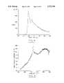
- FIG. 13shows growth rate in an Ar/H 2 /CH 4 plasma as determined by laser interferometry.
- the gas mixturecontained 1% CH 4 and the Ar/H 2 ratio was varied.
- the x-axis of FIG. 13is Ar!/ Ar+CH 4 +H 2 !.
- the growth rateincreases with increasing argon fraction to a peak value near a fraction of 0.75; the growth rate increases by nearly a factor of three over the argon-free condition;
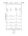
- FIG. 14shows an emission spectrum from a 100 sccm H 2 and 2 sccm CH 4 plasma; only H-alpha and H-beta emission lines from atomic hydrogen are observed;
- FIG. 15shows an emission spectrum from 25 sccm H 2 , 75 sccm Ar and 2 sccm CH 4 plasma; the C 2 Swan bands and atomic hydrogen lines are prominent, while the CH band at 4310 ⁇ and atomic argon lines at 7504 ⁇ and 7635 ⁇ are distinguishable;
- FIG. 16shows emission intensities from H (6560 ⁇ ), Ar (7504 ⁇ ), C 2 (5160 ⁇ band), and CH (4310 ⁇ band) plotted as a function of Ar fraction; C 2 emission increases by the greatest amount and increases in intensity relative to other emitting species, indicating an increase in gas phase concentration as the Ar flow increases.
- FIG. 17shows the growth rate as determined by laser interferometry. The rate increases linearly with CH 4 flow
- FIG. 18shows plasma Emission intensities observed as a function of growth rate for a second experiment; the C 2 emission increases linearly with growth rate, while emission from other species is nearly constant, identifying C 2 as the growth species;
- FIG. 19shows Raman spectra of the films produced in the two experiments; the lower spectrum is from the first experiment, where the Ar fraction in the reactor was varied; the upper spectrum is from the second experiment, where methane flow was increased;
- FIG. 20shows a (100) (2 ⁇ 1):H reconstructed diamond surface
- FIG. 21shows a C 2 molecule inserted into a C--C surface dimer bond
- FIG. 22shows a C 2 molecule inserted into an adjacent C--C surface dimer bond, forming a new surface dimer perpendicular to the previous dimer row;
- FIG. 23shows a second C 2 molecule forming a new surface dimer in an adjacent dimer row
- FIG. 24shows a third C 2 molecule inserted into the trough between the two previously incorporated C 2 molecules
- FIG. 25shows the third C 2 molecule completing insertion into the trough, forming a dimer row perpendicular to the previous surface row.
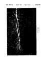
- FIG. 26shows an atomic force micrograph of an array of typical field emission tips
- FIG. 27Ashows a scanning electron microscope image of a diamond film grown in a H 2 /CH 4 plasma
- FIG. 27Bshows a transmission electron microscope image of a diamond layer prepared from a plasma of CH 4 /Ar
- FIG. 27Cshows a transmission electron microscope image of a diamond layer prepared from a plasma of Ar/C 60
- FIG. 27Dshows Atomic Force micrographs of diamond films grown from an H 2 --CH 4 plasma (upper figure) and from an Ar--C 60 plasma with very low (2%) hydrogen concentration.
- the vertical scalesare the same, illustrating a pronounced difference in surface roughness for the two processes.
- FIG. 28Ashows a schematic illustration of field emission tips and a diamond crystallite deposited on one of the tips using an H 2 --CH 4 plasma
- FIG. 28Bshows a schematic illustration of field emission tips covered with a layer of nanocrystalline diamond formed from a plasma of a noble gas and C 60 or CH 4 , C 2 H 2 or anthracene.
- FIG. 29is an atomic resolution TEM, of a diamond film grown in an Ar--C 60 plasma, showing atomically abrupt grain boundaries with no nondiamond intergranular material.
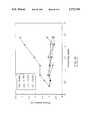
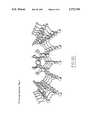
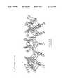
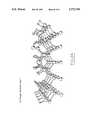
- FIG. 1A microwave plasma deposition system 10 (hereinafter "system 10") constructed in accordance with one form of the invention is illustrated in FIG. 1.
- the system 10is based on a ASTeX (PDS-17) commercial plasma deposition apparatus manufactured by Applied Science and Technology.
- Fullerene containing soot 12 used as a starting materialwas treated to remove hydrocarbon contaminants by contact with methanol.
- the treated soot 12was then thoroughly degassed by conventional vacuum and/or thermal treatment (such as heating at 200° C. for 2 hours).
- the degassed soot 12was placed in a sublimator 14 which is coupled to plasma deposition chamber 16, and the volume of the sublimator 14 is also coupled to the volume of the plasma deposition chamber 16.
- fullerene containing vapor 18can be introduced into the plasma deposition chamber 16 by heating the sublimator 14 (for example, by Pt resistance wire heating) to a temperature adequate to cause fullerene sublimation (such as, about 550° C. to 600° C.).
- a noble carrier gassuch as argon
- lower percentages (0-19%) of hydrogenare introduced through gas inlet 20 enabling the gas mixture to transport the sublimed fullerene containing vapor 18 into the plasma deposition chamber 16.
- a substrate 22was used to accumulate deposited carbon as a diamond layer on the substrate 22.
- the substrate 22can be a single crystal silicon wafer, or one of various metals or ceramics.
- the substrate 22can also be disposed on a graphite stage 24, which not only can support the substrate 22 but can act as a heating element to control the substrate temperature.
- a microwave generator 23Using a microwave generator 23, a microwave field 25 is established within the plasma deposition chamber 16 in order to generate an excited plasma 26.
- a variety of gas mixtures and other experimental conditionswere utilized to produce diamond layers, and a sampling of representative values are shown in Table 1. Films labeled A-E were grown to comparable thickness to allow direct comparison.
- Films F and Gwere grown to examine properties of thick films grown under the same conditions, Film G was grown under conventional H 2 --CH 4 conditions, and a bare silicon substrate was tested for comparison. Diamond film growth was monitored in situ using laser reflectance interferometry to determine growth rate and to allow stopping film growth at a selected thickness.
- the system 10operates to deposit diamond on the substrate 22, and the diamond samples produced were characterized by a variety of conventional materials characterization techniques, such as, X-ray diffraction, Auger electron spectroscopy (AES), electron diffraction, transmission and scanning electron microscopy, atomic force microscopy (AFM), electron energy loss spectroscopy, Raman spectroscopy. In addition, various wear rate tests were performed (see Table 1).
- Raman spectra of the filmswere measured with a Renishaw Raman microscope using a HeNe laser at 632.8 nm with an output of 25 mW focused to a spot size of about 2 nm.
- Raman spectroscopyis widely used to characterize diamond films, although the small grain sizes in these films has a significant effect on the Raman spectrum.
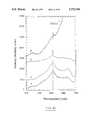
- Raman spectroscopyrevealed a band centered at 1333 cm -1 and a broad band feature at about 1550 cm -1 .
- the 1333 cm -1 bandis characteristic of all diamond films regardless of grain size, and the 1550 cm -1 band feature is also commonly observed from small grain size diamond films.
- a Phillips powder diffractometer with CuK.sub. ⁇ radiationwas used for XRD measurements to ensure the presence of diamond and check for evidence of crystalline graphite.
- X-ray diffraction examination of the diamond layersshowed the three major diamond diffraction peaks corresponding to the (111), (220) and (311) reflections (see FIG. 2).
- Particular regions of the diamond layerwere also examined by selected area electron diffraction and confined the lattice of the film was a face centered cubic structure with lattice constant of 3.53 ⁇ 0.10 Angstroms (the accepted diamond lattice constant is 3.56 Angstroms).
- AES spectrawere obtained using a Physical Electronics model 548 spectrometer with a double pass cylindrical mirror analyzer.
- the carbon KLL peak shapeis sensitive to the bonding state of carbon, providing a qualitative means of assessing the sp 2 /sp 3 ratio of the films.
- Near-edge extended X-ray absorption fine structure (NEXAFS) spectroscopyreveals structures corresponding to graphitic (sp 2 ) electron bonding between carbon atoms (286 eV), hydrogen-carbon bonding (288 eV) and diamond (sp 3 ) bonding between carbon atoms (290 eV).
- TEM imagingwas performed in the JEOL 4000EXII operating at 400 kV.
- Specimens for TEMwere prepared using standard dimpling and ion milling procedures. The surface was characterized using a Burleigh ARIS-3300 AFM to measure the rms surface roughness and a JEOL JXA-840A SEM to image the surface.
- Friction and wear testswere performed with pairs of silicon nitride balls and diamond-coated silicon substrates on a ball-on-disk tribometer. Tests were run in dry nitrogen environments. A Plexiglas cover was fitted over the tribometer, permitting ultra dry environments to be created. Several specimens without the diamond films were also tested, primarily to assess and compare their tribological performance to those with a diamond film. The dead weight applied to the balls was 2N. Frictional force was monitored with the aid of a linear variable-displacement-transducer and was recorded on a floppy disk via a data acquisition system throughout the tests. The rotational velocity was kept between 50 to 150 r/min.
- FIG. 12Ashows the friction coefficient of polished CVD diamond film as a function of surface roughness. Also shown are the measured friction coefficients of a cleaved single crystal natural diamond and an as-deposited diamond film deposited using an Ar--C 60 plasma. There is a strong correlation between the surface roughness and friction coefficient, and the Ar--C 60 film is close in both properties to the cleaved single crystal diamond sample.
- FIG. 12BThe measured friction coefficients for samples A and F in Table I as well as the uncoated Si substrate are shown in FIG. 12B. Referring to Table I and FIG. 12B, it can be seen that for a given carbon precursor, the hydrogen concentration in the plasma strongly affects the roughness and wear rates. The lowest friction and wear coefficients are obtained for low plasma hydrogen concentrations, and the films grown from the C 60 precursor tend to be smoother than those grown from the CH 4 precursor.
- additional diamond filmswere grown in the system 10 (a microwave plasma chemical vapor deposition reactor, ASTeX PDS-17 as previously described).
- the filmswere grown on silicon substrates polished with 0.1 ⁇ m diamond particles to enhance nucleation.
- In-situ diagnosticsincluded plasma emission spectroscopy and surface reflectivity measurements. Raman spectroscopy was performed on the films ex-situ to ensure that diamond films were in fact grown.
- Emission from the plasmawas collected with a quartz optical fiber by viewing a region 1-2 cm above the substrate 22.
- the lightwas transmitted to an Interactive Technology model 103 optical monochromator with entrance and exit slit widths of 50 ⁇ m and 400 ⁇ m respectively.
- the monochromatorwas stepped in 2.3 ⁇ increments with a dwell time of 100 msec from 3000 ⁇ to 8000 ⁇ .
- the dispersed lightwas detected with a Peltier-cooled photomultiplier tube.
- the reflectivity of the growing film surfacewas measured using a 5 mW HeNe laser.
- the reflected beamwas passed through a HeNe laser line filter to eliminate plasma emissions and detected with a photodiode.
- the oscillations in the reflectivitywere used to calculate the film thickness as a function of time and thus provide a measure of the growth rate.
- a Macintosh IIciwas used to control the spectrometer and acquire data from both the spectrometer and photodiode.
- Raman measurements of the filmswere performed with a Renishaw Raman microscope using a HeNe laser at 6328 ⁇ .
- Plasma emissionis observed when atoms or molecules in a plasma are excited to higher energy electronic states which decay mainly by radiative processes.
- the excited statesmay also decay by collisional quenching, and for larger molecules, by intermolecular nonradiative processes.
- many of the species in the plasma which are or interestfor example CH 3 . and C 2 H 2 , cannot be detected by plasma emission measurements.
- the emission intensity, proportional to the excited state population of the speciesis somewhat difficult to relate to the ground state population because changes in plasma conditions can produce changes in the emission intensity of a species by changing not only the ground state population, but also the excitation rate and the competing deexcitation mechanisms such as quenching. This makes use of plasma emission somewhat difficult for quantitative measurement of ground state species concentrations.
- the fraction of Ar in the reactorwas varied to determine the effect on growth rate and plasma emission for the five conditions shown in Table 3.
- the total flow of gas to the reactorwas kept constant with increasing amounts of argon substituted for hydrogen.
- the gas flowwas set and the emission spectrum measured after the growth ratio equilibrated.
- the growth rateis observed to increase with increasing argon fraction to a peak value for an argon fraction near 0.75 (data condition 4) as shown in FIG. 13.
- the argon additionleads to growth rates of up to a factor of three greater than that of hydrogen-methane.
- the change in gas compositionhas a large effect on the gas phase chemistry, as evidenced by the emission spectrum.
- H 2 and Ar flowswere maintained at 50 sccm while the CH 4 flow was varied from 1 to 5 sccm. Measurements of growth rate and plasma emission were made for seven conditions shown in Table 4. Again, for each condition the gas flow was set, and the emission spectrum was measured after the growth rate equilibrated.
- the growth rateincreased linearly with increasing CH 4 flow as shown in FIG. 17.
- the changes in CH 4 flowresult in small changes in the gas composition and can be thought of as a perturbation to the plasma. Since excitation and quenching rates can be expected to change only marginally under these conditions the emission intensity is likely correlated with ground state species concentrations in the plasma.
- the emission intensities of H, Ar, C 2 and CHare plotted as a function of growth rate in FIG. 18, normalized to unity at condition 1.
- the growth rateis unrelated to the H 2 , Ar and CH emission intensities, but increases linearly with C 2 emission intensity.
- the growth ratedepends on the C 2 gas phase concentration in the plasma.
- ⁇is the laser wavelength (0.6328 ⁇ m)
- mis the number of oscillations in the reflectance (31.5)
- dis the film thickness (4.0 ⁇ 0.3 ⁇ m). From this, the index of refraction of the film is calculated to be 2.5 ⁇ 0.2. This is within error of the accepted value of 2.41 for bulk diamond at this wavelength.
- C 2 deposition to form diamondis energetically favorable.
- Ab initio calculationsindicate that C 2 insertion into the reconstructed hydrogen-terminated (100) surface of diamond is energetically favorable with small activation barriers. It has been experimentally determined that diamond films can, using this process, be grown at relatively low temperatures ( ⁇ 500° C.), as opposed to conventional diamond growth processes which require substrate temperatures of 800° C.-1000° C. These high substrate temperatures preclude deposition on many materials of technological importance.
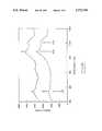
- FIGS. 20-25a proposed mechanism for growth on the diamond (100) (2 ⁇ 1):H reconstructed surface with C 2 is outlined.
- FIG. 20shows the (100) (2 ⁇ 1):H reconstructed diamond surface, thought to be the most likely surface in these environments. The large atoms are C and the small atoms are H terminating the surface.
- a C 2 moleculeimpinges on the surface and inserts into a surface C--C dimer bond, as shown in FIG. 21. The C 2 then inserts into an adjacent C--C bond to form a new surface carbon dimer, as shown in FIG. 22.
- a second C 2 moleculeforms a new surface dimer on an adjacent row, as shown in FIG. 23.
- a third C 2 moleculeinserts into the trough between the two new surface dimers as shown in FIGS. 24 and 25.
- the three C 2 molecules incorporated into the diamond surfaceform a new surface dimer row running perpendicular to the previous dimer row.
- the C 2 growth mechanism as proposed hererequires no hydrogen abstraction reactions from the surface and in principle should proceed in the absence of gas phase atomic hydrogen.
- the previously described methods of manufacturecan be applied to produce equiaxed nanocrystalline diamond film and fine grained dendritic structures.
- Such preferred structuresare advantageous for specialized applications calling for very uniform, fine grained diamond which is quite smooth and can be reliably produced as layers of extremely small thickness.
- diamond layerscan be used to great advantage on field emission microtips (or any such electronic or optical application) which require deposition of a very thin, smooth conformal diamond coating which preserves the topographical features of the substrate.
- Diamondhas been shown to be a cold cathode electron emitting material with emission characteristics which follow the known Fowler-Nordheim relation corresponding to field-induced electron tunneling.
- the materialmust (1) have the low work function/negative electron affinity of diamond, (2) have sufficient electrical conductivity to provide a conducting path to the substrate in order to restore the emitted electrons to the surface, (3) for planar emitters, the film should have a surface topography which enhances the electric field at the surface and (4) for microtip arrays, the film should have a morphology which produces a uniform thin coating on microtips which have contour requirements on the 10-100 nm scale.
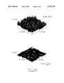
- Microtip arraystypically are very well defined tips 100 as shown in FIGS. 26 and 28. These tips 100 are typically made of silicon using photolithography techniques developed by the semiconductor industry and have submicron size dimensions. Conventional diamond layer deposition techniques produce the morphology of diamond crystals 102 shown in FIG. 27A and FIG. 28A. Such structures would not enable use of diamond coated microtips as field emitters.
- FIG. 9.This figure is a cross-section TEM which shows a 20-30 nm thick film which has a continuity and density unattainable by conventional diamond growth processes.
- a highly equiaxed, nanocrystalline diamond film(average grain size of 15 nm and range of 10-30 nm) can be deposited using one of the methods described herein (see Examples I and VIII). Moreover, as noted in Example V, there is no evidence of graphite formation which further enhances the suitability of the diamond film to a variety of electronic applications.
- Example IXthe electronic properties of the above-described diamond layers are well suited for use as field emission tips and other demanding electronic applications.
- a C 60 sublimation sourcewas coupled to a microwave chamber operated with a microwave generator at 2.45 GHz as shown in FIG. 1.
- the system as a wholeis an ASTeX PDS-17 unit supplied by Applied Science and Technology.
- Fullerene containing sootwas made in a conventional manner or was obtained from MER Corporation. (e.g., about 10% C 60 in the soot).
- the sootwas treated with methanol to remove most of the hydrocarbon constituents.
- the cleaned sootwas place in a gold container which in turn was disposed in a quartz tube wound with nichrome wire used to heat the soot.
- the microwave chamberwas evacuated and the soot heated to about 200° C.-250° C.
- the rate of C 60 sublimationwas determined by placing a silicon wafer in front of the outlet of the sublimation source inside the microwave chamber. An argon gas flow of 20 sccm with a total pressure in the chamber of 100 Torr was established by use of a carrier gas inlet into the sublimation source. The sublimation source was maintained at about 500° C., and adequate C 60 was deposited in one-half an hour on the silicon single crystal (maintained at temperatures above about 470° C. so that a typical C 60 infrared absorption spectrum could be easily noted. Raman spectroscopy confirmed the presence of C 60 . There were no features in the infrared spectrum that could be attributed to species other than C 60 .
- Example IIThe same manufacturing procedure set forth in Example I was followed except the silicon wafer was removed, and fresh soot was placed in the sublimation source.
- the temperature of the sublimation sourcewas raised to about 500° C.
- the microwave generatorwas activated and a 500 watt microwave discharge was initiated at 1 Torr argon.
- a quartz fiber optic cablewas coupled to the microwave chamber to enable viewing of the plasma discharge at a region about 1-1.5 cm above the silicon substrate.
- the light within the fiber optic cablewas transmitted to an Interactive Technology model 103 optical monochromator with 200 micron entrance and exit slit widths.
- the monochromator wavelengthwas stepped in increments of about 2.3 Angstroms with a dwell time of about 100 msec/step.
- the light detectorwas a Peltier cooled photomultiplier tube operating in a pulse counting mode with a dark count rate of 20-30 cps.
- a Macintosh IIci control computerwas used with software to provide a 100 msec gating pulse to the 32-bit National Instruments counter board located in the computer back plane.
- FIG. 3AA typical spectrum obtained from the intensely emerald green plasma discharge is shown in FIG. 3A.
- FIG. 3AAn examination of the Swan bands in FIG. 3A was performed by analyzing emission spectra as a function of sublimator source temperature.
- the Swan band emission intensitieswere found to increase as a function of sublimator temperature (see FIG. 3C).
- the emission intensitiesshould follow the vapor pressure of C 60 (see FIG. 3C, curve B).
- a log plotclearly shows that the argon carrier gas is far from being saturated with the equilibrium C 60 pressure.
- the C 2 concentration in the plasmaincreases with temperature due to increased C 60 volatility which shows the C 2 emission is not a minor constituent, nor is it due to carbon particles transported into the plasma.
- Example IIThe same basic method of Example II was followed except the microwave power level was varied from 500 to 1200 watts. There was no noticeable change in the absolute intensity or the intensity ratios of the different Swan band frequencies.
- the growth rate of diamond film in Example IIwas characterized to be about 1.2 microns/hour which is comparable to or higher than the deposition rate obtained with a conventional plasma containing 1% methane in hydrogen.
- Conventional diamond films grown at this ratehave a very large grain size, rough surface and high defect density.
- By lowering the pressure to ⁇ 300 mTorr and confining the plasma with a magnetic fieldit is possible to reduce the defect density, grain size and surface roughness, but there is a sharp drop in growth rate.
- Smooth filmscan be obtained at high growth rate (0.5-1 micron/hr) by increasing the CH 4 content of the plasma, but the resulting films have an increased graphitic content.
- the films produced using the subject inventionshow much smaller defect density than conventional films prepared at 300 mTorr with a magnetized plasma using CH 4 --H 2 --O 2 mixtures as prepared by the applicants herein.
- the films prepared by the method of the inventionalso show no evidence of graphite contamination, and exhibit atomically abrupt grain boundaries with no nondiamond intergranular material.
- the growth rates obtained with the method of the inventionwere comparable with the high pressure growth rate obtained with the standard method, and 10-100 ⁇ higher than obtained at 300 mTorr using standard plasma composition.
- Example IThe procedure described in Example I was followed except that the chamber pressure was 50 mTorr, using an Ar flow rate >10 sccm with an upper magnet current of 150 A and a lower magnet current of 115 A to improve plasma stability.
- the microwave powerwas 500 watts, and the fullerene sublimator heater was operated at 110 volts, resulting in a sublimation source temperature of about 500° C.
- fullerene rich sootis replaced by a flow of CH 4 gas as the source of carbon for the diamond.
- the experimental conditions for the deposition system 10are set forth in Table 1 for Films D-G.
- acetylene (C 2 H 2 )was also used under similar conditions as CH 4 and diamond was produced.
- FIG. 7shows XRD patterns from Films B-F.
- the characteristic (111), (220) and (311) diamond peaksare evident.
- the strong Si (400) peak due to the silicon substratehas been removed.
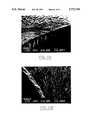
- FIG. 9shows a HRTEM image of a section of Film A.
- the silicon substratehas been removed and a layer of gold deposited on the diamond.
- a 100 ⁇ thick layer composed of amorphous carbon and diamondwas immediately above the silicon substrate and formed preceding diamond film growth.
- the diamond grainsare clearly visible above the amorphous layer and appear as well ordered diamond crystals.
- the boundaries between the grainsare sharp and appear to contain little or no nondiamond phases. This is demonstrated even more clearly by FIG. 29 which shows a grain boundary region at atomic resolution.
- the lines in this figureare the atomic rows, and the spacing matches that of the bulk diamond lattice, unambiguously demonstrating formation of the diamond phase and the lack of any nondiamond phase at the grain boundary. This further indicates these films are composed of nanocrystalline diamond films with little sp 2 carbon present.
- Raman spectra of Films A-C and Gwhich are representative of all the films grown are shown in FIG. 10.
- Raman spectra of Films E and Fare similar to Film C while the Raman spectrum of Film D is similar to Film B.
- the Raman spectrashow a peak at 1332 cm -1 attributed to diamond.
- Features at 1580 and 1330 cm -1have been attributed to sp 2 carbon but probably are due to atoms residing at grain boundaries in this nanocrystalline material.
- An additional feature around 1140 cm -1appears for Films A and C which has been attributed to nanocrystalline diamond.
- an intense fluorescence peak at 2250 cm -1 (1.68 eV)results in the rapidly rising background.
- the weak 1332 cm -1 peak relative to other Raman features for films grown at low hydrogen contentsis attributed to the small grain size in the films rather than an increase in the sp 2 /sp 3 carbon ratio.
- the 1332 cm -1 peak intensityhas been shown to decrease with decreasing grain size both for diamond particles of known size and diamond films, where the grain size was determined from XRD measurements.
- these Raman spectrawere excited using 632.8 nm light, which is more sensitive to the nondiamond carbon phases than the 488 nm Argon ion laser light commonly employed for measuring Raman spectra.
- AFM measurements(see Table 1) of rms surface roughness for Films A-E and G, all grown to ⁇ 2 ⁇ m, shows that higher carbon to hydrogen ratios lead to smooth film growth, while lower ratios lead to rougher films.
- Film Fdemonstrates that in these low hydrogen content plasmas, a 10 ⁇ m thick, smooth (rms roughnesses of 45 nm) film can be grown.
- FIG. 11Ais a cross-sectional SEM micrograph of Film A. As is clear, the surface of this nanocrystalline diamond Film is rather smooth. FIG. 11B shows that the wear track formed on Film A during tribological testing becomes extremely smooth.
- FIG. 12Ashows the measured coefficient of friction for conventionally grown polished CVD diamond film as a function of surface roughness. Also shown are the friction coefficients for a cleaved single crystal natural diamond and an unpolished film grown from an Ar--C 60 plasma. The cleaved natural diamond and the Ar--C 60 grown film have comparable surface roughness and identical friction properties. As is evident from FIG. 12B, Film G with a rough surface finish exhibits a significantly higher friction coefficient than the smooth Film C in dry N 2 . As a reference, the friction coefficient of the Si substrate against the Si 3 N 4 ball is also included in FIG. 12B. The friction coefficient of the rough diamond Film G was somewhat higher than that of the Si substrate, and the wear rate of the counterface material is considerably higher.
- Table 1shows the overall frictional performance and ball wear rate for both the rough and smooth diamond films. Again, the highest friction coefficients are due to rough diamond films, whereas the smooth diamond films exhibit friction coefficients of 0.04 to 0.12. We believe that the large fluctuations in the friction traces and very high initial friction coefficients of rough diamond films are largely due to ploughing and interlocking of asperities across the sliding interface. Sharp asperity tips of diamond crystals can dig in and cut the surface of softer counterface material, thus causing severe abrasion and ploughing. It is known that a high degree of ploughing can cause high frictional traction between sliding surfaces. This in turn promotes high friction and severe abrasion of the much softer counterface material.
- Films A and Cexhibit very low friction coefficients, i.e., 0.04 to 0.12, especially at steady-state (see FIG. 12B). These values are comparable to that of a natural diamond in dry N 2 as conventionally reported. As shown in FIG. 11A, the surface asperities of these films are not faceted and sharp. Most importantly, the sliding contact surfaces of these films become exceedingly smooth under the influence of repeated sliding (see FIG. 11B). As a result, the extent of frictional losses during sliding against Si 3 N 4 remain low, especially after a break-in regime of the sliding tests. In short, these films cause much lower ploughing, hence very little fluctuation in friction traces during sliding.
- Table 1lists the wear rates of Si 3 N 4 balls during sliding against various diamond films. As is evident, compared to smooth diamond films, rough diamond films cause much higher wear losses on counterface balls. This can be attributed to severe abrasion caused by the sharp asperity tips and edges of rough diamond crystals, whereas the smooth films result in much lower wear losses on the Si 3 N 4 ball, up to 100 ⁇ lower than previously reported values for conventionally deposited diamond thin films.
Landscapes
- Chemical & Material Sciences (AREA)
- Organic Chemistry (AREA)
- Engineering & Computer Science (AREA)
- Materials Engineering (AREA)
- Metallurgy (AREA)
- Chemical Kinetics & Catalysis (AREA)
- Crystallography & Structural Chemistry (AREA)
- Mechanical Engineering (AREA)
- Inorganic Chemistry (AREA)
- General Chemical & Material Sciences (AREA)
- Life Sciences & Earth Sciences (AREA)
- General Life Sciences & Earth Sciences (AREA)
- Geology (AREA)
- Physics & Mathematics (AREA)
- Combustion & Propulsion (AREA)
- Plasma & Fusion (AREA)
- Manufacturing & Machinery (AREA)
- Carbon And Carbon Compounds (AREA)
- Crystals, And After-Treatments Of Crystals (AREA)
Abstract
Description
TABLE 1 __________________________________________________________________________ H.sub.2 Ar CH.sub.4 C.sub.60 Substr Growth Diamond RMS Wear Rate Sample Flow Flow Flow T-furn Pres. Power Temp Rate Thickness Roughness Friction × 10.sup.-6 Film ID# sccm sccm sccm °C. Torr W °C. μm/hr μm nm Coef. mm.sup.3 /Nm __________________________________________________________________________A 940825 2 100 0 600 100 1500 850 0.3 1.7 30 0.12 0.01410 90 0 630 100 1500 850 0.9 2.0 105 0.18 0.15 C 940927 2 98 0 630 100 1500 850 0.25 2.0 41 0.04 0.1 B 940926BD 940928 10 90 0.8 20 100 1500 850 0.8 2.0 125 0.21 0.88E 940929 1.5 98 0.8 20 100 1500 850 0.5 2.3 53 0.08 0.4 F 941013 2 100 1 20 100 800 850 0.7 10 45 -- -- G 950802 98 0 2 20 60 1500 800 0.5 6 376 0.3 5.5 Silicon -- -- -- -- -- -- -- -- 0 <3 0.42 1.2 __________________________________________________________________________
TABLE 2 ______________________________________ Excited State Species Transition Wavelength Å Energy (eV) ______________________________________ H .sup.2 P.sup.0 3/2→.sup.2 S1/2 6560 12.1 Ar 4.sub.p ' 1/2!.sub.o →4s' 1/2!1.sup.0 7504 13.5 C.sub.2 d.sup.3 Π.sub.g →a.sup.3 Π.sub.u 5165(0-0) 2.5 CH A.sup.2 Δ→X.sup.2 Π.sub.r 4314(0-0) 2.9 ______________________________________
TABLE 3 ______________________________________ Power: 1500 W Pressure: 80 Torr Temperature: 850° C. H.sub.2 Flow Ar Flow CH.sub.4 Flow Data Point (sccm) (sccm) (sccm) ______________________________________ 1 100 0 2 2 75 25 2 3 50 50 2 4 25 75 2 5 10 90 2 ______________________________________
TABLE 4 ______________________________________ Power: 1500 W Pressure: 100 Torr Temperature: 850° C. H.sub.2 Flow Ar Flow CH.sub.4 Flow Point (sccm) (sccm) (sccm) ______________________________________ 1 50 50 1 2 50 50 1.5 3 50 50 2 4 50 50 2.5 5 50 50 3 6 50 50 4 7 50 50 5 ______________________________________
n=mλ/2d,
Claims (30)
Priority Applications (3)
| Application Number | Priority Date | Filing Date | Title |
|---|---|---|---|
| US08/540,916US5772760A (en) | 1991-11-25 | 1995-10-11 | Method for the preparation of nanocrystalline diamond thin films |
| PCT/US1996/016119WO1997013892A1 (en) | 1995-10-11 | 1996-10-08 | Improved method for the preparation of nanocrystalline diamond thin films |
| AU72609/96AAU7260996A (en) | 1995-10-11 | 1996-10-08 | Improved method for the preparation of nanocrystalline diamond thin films |
Applications Claiming Priority (4)
| Application Number | Priority Date | Filing Date | Title |
|---|---|---|---|
| US07/797,590US5209916A (en) | 1991-11-25 | 1991-11-25 | Conversion of fullerenes to diamond |
| US08/035,419US5370855A (en) | 1991-11-25 | 1993-03-23 | Conversion of fullerenes to diamond |
| US08/143,866US5620512A (en) | 1993-10-27 | 1993-10-27 | Diamond film growth from fullerene precursors |
| US08/540,916US5772760A (en) | 1991-11-25 | 1995-10-11 | Method for the preparation of nanocrystalline diamond thin films |
Related Parent Applications (1)
| Application Number | Title | Priority Date | Filing Date |
|---|---|---|---|
| US08/143,866Continuation-In-PartUS5620512A (en) | 1991-11-25 | 1993-10-27 | Diamond film growth from fullerene precursors |
Publications (1)
| Publication Number | Publication Date |
|---|---|
| US5772760Atrue US5772760A (en) | 1998-06-30 |
Family
ID=24157441
Family Applications (1)
| Application Number | Title | Priority Date | Filing Date |
|---|---|---|---|
| US08/540,916Expired - LifetimeUS5772760A (en) | 1991-11-25 | 1995-10-11 | Method for the preparation of nanocrystalline diamond thin films |
Country Status (3)
| Country | Link |
|---|---|
| US (1) | US5772760A (en) |
| AU (1) | AU7260996A (en) |
| WO (1) | WO1997013892A1 (en) |
Cited By (57)
| Publication number | Priority date | Publication date | Assignee | Title |
|---|---|---|---|---|
| US6087765A (en)* | 1997-12-03 | 2000-07-11 | Motorola, Inc. | Electron emissive film |
| US6258417B1 (en) | 1998-11-24 | 2001-07-10 | Research Foundation Of State University Of New York | Method of producing nanocomposite coatings |
| WO2001057295A1 (en)* | 2000-01-27 | 2001-08-09 | The University Of Chicago | Patterning of nanocrystalline diamond films for diamond microstructures useful in mems and other devices |
| US6356006B1 (en)* | 1997-10-06 | 2002-03-12 | Sumitomo Electric Industries, Ltd. | Diamond wafer, method of estimating a diamond wafer and diamond surface acoustic wave device |
| US6364662B1 (en) | 1998-11-12 | 2002-04-02 | Nobel Biocare Ab | Diamond-like carbon coated dental instrument |
| US6416820B1 (en) | 1999-11-19 | 2002-07-09 | Epion Corporation | Method for forming carbonaceous hard film |
| US6447295B1 (en) | 1999-04-15 | 2002-09-10 | Nobel Biocare Ab | Diamond-like carbon coated dental retaining screws |
| US20020169114A1 (en)* | 2001-01-25 | 2002-11-14 | The United States Of America, Represented By The Secretary, Department Of Health And Human Services | Formulation of boronic acid compounds |
| US6547562B2 (en) | 2000-05-11 | 2003-04-15 | Nobel Biocare Ab | Pseudo-etching of diamond-like carbon coated instruments |
| US20030152700A1 (en)* | 2002-02-11 | 2003-08-14 | Board Of Trustees Operating Michigan State University | Process for synthesizing uniform nanocrystalline films |
| US20030160542A1 (en)* | 2002-01-25 | 2003-08-28 | Board Of Trustees Of Michigan State University | Surface acoustic wave devices based on unpolished nanocrystalline diamond |
| US20030171646A1 (en)* | 2000-04-11 | 2003-09-11 | Advanced Biomedical Devices, Inc. | Implant positioning system and method |
| US20030170906A1 (en)* | 2002-01-23 | 2003-09-11 | Board Of Trustees Of Michigan State University | Conductive diamond spectrographic cells and method of use |
| WO2003078874A2 (en) | 2002-03-11 | 2003-09-25 | Second Sight, Llc | Coated microfluidic delivery system |
| US6667070B1 (en)* | 2001-02-02 | 2003-12-23 | Advanced Micro Devices, Inc. | Method of in situ monitoring of thickness and composition of deposited films using raman spectroscopy |
| US6689453B2 (en) | 1998-11-24 | 2004-02-10 | Research Foundation Of State University Of New York | Articles with nanocomposite coatings |
| US20040220667A1 (en)* | 2003-02-07 | 2004-11-04 | Vladimir Gelfandbein | Implantable device using diamond-like carbon coating |
| US20040221796A1 (en)* | 2002-01-11 | 2004-11-11 | Board Of Trustees Of Michigan State University | Electrically conductive polycrystalline diamond and particulate metal based electrodes |
| US20040258918A1 (en)* | 2003-06-19 | 2004-12-23 | Chaffin John Harvie | Diamond films and methods of making diamond films |
| US20050031785A1 (en)* | 2003-08-07 | 2005-02-10 | The University Of Chicago | Method to grow pure nanocrystalline diamond films at low temperatures and high deposition rates |
| US20050102178A1 (en)* | 2003-11-07 | 2005-05-12 | Phillips Daniel W. | Systems and methods for generating multiple revenue streams involving the use of an integrated appliance |
| US20050154662A1 (en)* | 2003-11-06 | 2005-07-14 | Langenwalter James A. | Asset allocation, rebalancing, and investment management system |
| US20060175953A1 (en)* | 2002-01-11 | 2006-08-10 | Board Of Trustees Of Michigan State University | Electrically conductive diamond electrodes |
| US20060222772A1 (en)* | 2005-03-31 | 2006-10-05 | Bao Feng | Method and apparatus for the production of thin film coatings |
| US20060235475A1 (en)* | 2001-02-28 | 2006-10-19 | Mech Brian V | Implantable device using ultra-nanocrystalline diamond |
| US20070082200A1 (en)* | 2005-10-11 | 2007-04-12 | Gruen Dieter M | An Apparatus, Method, and Article of Manufacture Corresponding to a Self-Composite Comprised of Nanocrystalline Diamond and a Non-Diamond Component that is Useful for Thermoelectric Applications |
| US20070110644A1 (en)* | 2003-12-03 | 2007-05-17 | Yasuhiko Kasama | System for manufacturing a fullerene derivative and method for manufacturing |
| US20070137684A1 (en)* | 2005-10-11 | 2007-06-21 | Gruen Dieter M | Method and Article of Manufacture Corresponding To a Composite Comprised of Ultra Nanocrystalline Diamond, Metal, and Other Nanocarbons Useful for Thermoelectric and Other Applications |
| US20070205521A1 (en)* | 2006-01-27 | 2007-09-06 | Lockheed Martin Corporation | Encapsulation of Semiconductor Components |
| US20070281075A1 (en)* | 2006-05-31 | 2007-12-06 | Cheng-Chia Huang | Optical method to monitor nano thin-film surface structure and thickness thereof |
| US20090017258A1 (en)* | 2007-07-10 | 2009-01-15 | Carlisle John A | Diamond film deposition |
| WO2006130739A3 (en)* | 2005-05-31 | 2009-04-23 | Univ California | Graphitized carbon coatings for composite electrodes |
| US20090173950A1 (en)* | 2008-01-04 | 2009-07-09 | Advanced Diamond Technologies | Controlling diamond film surfaces and layering |
| US7560793B2 (en) | 2002-05-02 | 2009-07-14 | Micron Technology, Inc. | Atomic layer deposition and conversion |
| US7575978B2 (en) | 2005-08-04 | 2009-08-18 | Micron Technology, Inc. | Method for making conductive nanoparticle charge storage element |
| US20090214826A1 (en)* | 2008-01-04 | 2009-08-27 | Charles West | Controlling diamond film surfaces |
| US7667570B1 (en)* | 2004-05-19 | 2010-02-23 | Lockheed Martin Corporation | Nanostructured combination key-lock |
| US7670646B2 (en) | 2002-05-02 | 2010-03-02 | Micron Technology, Inc. | Methods for atomic-layer deposition |
| US7687146B1 (en) | 2004-02-11 | 2010-03-30 | Zyvex Labs, Llc | Simple tool for positional diamond mechanosynthesis, and its method of manufacture |
| US20100089773A1 (en)* | 2002-06-10 | 2010-04-15 | Trustees Of Tufts College | Total organic compound (toc) analyzer |
| US20100267160A1 (en)* | 2006-02-09 | 2010-10-21 | OI Analytical | Total Organic Carbon Analysis |
| US20110005564A1 (en)* | 2005-10-11 | 2011-01-13 | Dimerond Technologies, Inc. | Method and Apparatus Pertaining to Nanoensembles Having Integral Variable Potential Junctions |
| US7927948B2 (en) | 2005-07-20 | 2011-04-19 | Micron Technology, Inc. | Devices with nanocrystals and methods of formation |
| US7989290B2 (en) | 2005-08-04 | 2011-08-02 | Micron Technology, Inc. | Methods for forming rhodium-based charge traps and apparatus including rhodium-based charge traps |
| US8367506B2 (en) | 2007-06-04 | 2013-02-05 | Micron Technology, Inc. | High-k dielectrics with gold nano-particles |
| US8586999B1 (en) | 2012-08-10 | 2013-11-19 | Dimerond Technologies, Llc | Apparatus pertaining to a core of wide band-gap material having a graphene shell |
| US8829331B2 (en) | 2012-08-10 | 2014-09-09 | Dimerond Technologies Llc | Apparatus pertaining to the co-generation conversion of light into electricity |
| US9040395B2 (en) | 2012-08-10 | 2015-05-26 | Dimerond Technologies, Llc | Apparatus pertaining to solar cells having nanowire titanium oxide cores and graphene exteriors and the co-generation conversion of light into electricity using such solar cells |
| US9343275B1 (en)* | 2012-06-06 | 2016-05-17 | Western Digital (Fremont), Llc | Methods for characterizing carbon overcoat |
| DE10149588B4 (en)* | 2001-10-08 | 2017-09-07 | Oerlikon Trading Ag, Trübbach | Process for diamond coating of substrates |
| CN110872119A (en)* | 2018-08-31 | 2020-03-10 | 郑州大学 | Method for synthesizing superfine diamond micro powder |
| US10833285B1 (en) | 2019-06-03 | 2020-11-10 | Dimerond Technologies, Llc | High efficiency graphene/wide band-gap semiconductor heterojunction solar cells |
| US11471172B1 (en) | 2018-12-06 | 2022-10-18 | Gary Bram | Osteotomy drill bit to produce an optimally shaped jawbone opening for a dental implant and abutment |
| CN115928051A (en)* | 2022-11-29 | 2023-04-07 | 香港中文大学(深圳) | Diamond nanoneedle array light-absorbing layer and preparation method thereof |
| US12167951B1 (en) | 2022-01-20 | 2024-12-17 | Gary Bram | Osteotomy drill bit to produce an optimally shaped jawbone opening for a dental implant and abutment |
| US12220296B1 (en) | 2018-12-06 | 2025-02-11 | Gary Bram | Osteotomy drill bit to produce an optimally shaped jawbone opening for a dental implant and abutment |
| USD1088228S1 (en) | 2019-12-05 | 2025-08-12 | Gary Bram | Osteotomy drill |
Families Citing this family (2)
| Publication number | Priority date | Publication date | Assignee | Title |
|---|---|---|---|---|
| DE10259174B4 (en) | 2002-12-18 | 2006-10-12 | Robert Bosch Gmbh | Use of a tribologically stressed component |
| CN105296966B (en)* | 2015-11-16 | 2017-11-03 | 哈尔滨工业大学 | Power othermohygrometer coupling process in microwave enhancing plasma activated chemical vapour deposition |
Citations (11)
| Publication number | Priority date | Publication date | Assignee | Title |
|---|---|---|---|---|
| US4559901A (en)* | 1984-01-31 | 1985-12-24 | Futaba Denshi Kogyo K.K. | Ion beam deposition apparatus |
| US4634600A (en)* | 1984-06-29 | 1987-01-06 | Sumitomo Electric Industries, Ltd. | Surface treatment process |
| US4816286A (en)* | 1985-11-25 | 1989-03-28 | Showa Denko Kabushiki Kaisha | Process for synthesis of diamond by CVD |
| US5015494A (en)* | 1987-02-24 | 1991-05-14 | Semiconductor Energy Laboratory Co., Ltd. | Microwave enhanced CVD method for depositing diamond |
| US5132105A (en)* | 1990-02-02 | 1992-07-21 | Quantametrics, Inc. | Materials with diamond-like properties and method and means for manufacturing them |
| US5209916A (en)* | 1991-11-25 | 1993-05-11 | Gruen Dieter M | Conversion of fullerenes to diamond |
| US5273788A (en)* | 1992-07-20 | 1993-12-28 | The University Of Utah | Preparation of diamond and diamond-like thin films |
| US5360477A (en)* | 1992-03-04 | 1994-11-01 | Semiconductor Energy Laboratory Co., Ltd. | Method for forming diamond and apparatus for forming the same |
| US5370855A (en)* | 1991-11-25 | 1994-12-06 | Gruen; Dieter M. | Conversion of fullerenes to diamond |
| US5449531A (en)* | 1992-11-09 | 1995-09-12 | North Carolina State University | Method of fabricating oriented diamond films on nondiamond substrates and related structures |
| US5529815A (en)* | 1994-11-03 | 1996-06-25 | Lemelson; Jerome H. | Apparatus and method for forming diamond coating |
- 1995
- 1995-10-11USUS08/540,916patent/US5772760A/ennot_activeExpired - Lifetime
- 1996
- 1996-10-08AUAU72609/96Apatent/AU7260996A/ennot_activeAbandoned
- 1996-10-08WOPCT/US1996/016119patent/WO1997013892A1/enactiveApplication Filing
Patent Citations (13)
| Publication number | Priority date | Publication date | Assignee | Title |
|---|---|---|---|---|
| US4559901A (en)* | 1984-01-31 | 1985-12-24 | Futaba Denshi Kogyo K.K. | Ion beam deposition apparatus |
| US4634600A (en)* | 1984-06-29 | 1987-01-06 | Sumitomo Electric Industries, Ltd. | Surface treatment process |
| US4816286A (en)* | 1985-11-25 | 1989-03-28 | Showa Denko Kabushiki Kaisha | Process for synthesis of diamond by CVD |
| US5015494A (en)* | 1987-02-24 | 1991-05-14 | Semiconductor Energy Laboratory Co., Ltd. | Microwave enhanced CVD method for depositing diamond |
| US5132105A (en)* | 1990-02-02 | 1992-07-21 | Quantametrics, Inc. | Materials with diamond-like properties and method and means for manufacturing them |
| US5370855A (en)* | 1991-11-25 | 1994-12-06 | Gruen; Dieter M. | Conversion of fullerenes to diamond |
| US5328676A (en)* | 1991-11-25 | 1994-07-12 | Gruen Dieter M | Conversion of fullerenes to diamond |
| US5209916A (en)* | 1991-11-25 | 1993-05-11 | Gruen Dieter M | Conversion of fullerenes to diamond |
| US5462776A (en)* | 1991-11-25 | 1995-10-31 | Gruen; Dieter M. | Conversion of fullerenes to diamonds |
| US5360477A (en)* | 1992-03-04 | 1994-11-01 | Semiconductor Energy Laboratory Co., Ltd. | Method for forming diamond and apparatus for forming the same |
| US5273788A (en)* | 1992-07-20 | 1993-12-28 | The University Of Utah | Preparation of diamond and diamond-like thin films |
| US5449531A (en)* | 1992-11-09 | 1995-09-12 | North Carolina State University | Method of fabricating oriented diamond films on nondiamond substrates and related structures |
| US5529815A (en)* | 1994-11-03 | 1996-06-25 | Lemelson; Jerome H. | Apparatus and method for forming diamond coating |
Non-Patent Citations (30)
| Title |
|---|
| Annu. Rev. Mater. Sci., vol. 21, 1991, pp. 221 248, Metastable Growth of Diamond and Diamond Like Phases, Angus, Wang and Sunkara.* |
| Annu. Rev. Mater. Sci., vol. 21, 1991, pp. 221-248, "Metastable Growth of Diamond and Diamond-Like Phases," Angus, Wang and Sunkara. |
| Appl. Phys. Lett., Dec. 23, 1991, p. 3461, Nucleation of Diamond Films on Surfaces Using Carbon Clusters, Authors: R.J. Meilunas and R.P.H. Chang.* |
| Chem, Rev., 1991, 91, pp. 1213 1235, C 60 Buckminsterfullerene Authors: Kroto et al.* |
| Chem, Rev., 1991, 91, pp. 1213-1235, "C60 Buckminsterfullerene" Authors: Kroto et al. |
| Chemical Physics Letters, Dec. 20, 1991, "Near Specular Reflection of C60 Ions in Collisions with an HOPG Graphite Surface," Authors: Busmann, Lill and Hertel. |
| Chemical Physics Letters, Dec. 20, 1991, Near Specular Reflection of C 60 Ions in Collisions with an HOPG Graphite Surface, Authors: Busmann, Lill and Hertel.* |
| Cheng et al., "Fabrication and Charaterizing of Diamond -Clad Silicon", Japanese Journal of Applied Physics, Part I, vol. 34, No. 12B, pp. 6926-31. |
| Cheng et al., Fabrication and Charaterizing of Diamond Clad Silicon , Japanese Journal of Applied Physics, Part I, vol. 34, No. 12B, pp. 6926 31.* |
| J. Chem, Phys., Dec. 1990, p. 7800, Laser Deposition of Carbon Clusters on Surfaces: A New Approach to the Study of Fullerenes, Authors: Gerard Meijer and Donald S. Bethune.* |
| J. Chem. Phys., vol. 95, Nov. 1, 1991, pp. 7008 7010, Delayed electron emission from photoexcited C 60 , Authors: Wurz et al.* |
| J. Chem. Phys., vol. 95, Nov. 1, 1991, pp. 7008-7010, "Delayed electron emission from photoexcited C60," Authors: Wurz et al. |
| J. Mater. Res., Jan./Feb. 1988, pp. 133 139, Growth mechanism of vapor deposited diamond, Authors: Frenklach et al.* |
| J. Mater. Res., Jan./Feb. 1988, pp. 133-139, "Growth mechanism of vapor-deposited diamond," Authors: Frenklach et al. |
| J. Phys. Chem, vol. 95, 1991, pp. 8402 8409, Resilience of All Carbon Molecules C 60, C 70 and C 84 : A Surface Scattering Time of Flight Investigation, Author: Beck, St. John, Alvarez, Diedrich and Whetten.* |
| J. Phys. Chem, vol. 95, 1991, pp. 8402-8409, "Resilience of All-Carbon Molecules C60, C70 and C84 : A Surface-Scattering Time-of-Flight Investigation," Author: Beck, St. John, Alvarez, Diedrich and Whetten. |
| Mat. Res. Soc. Symp. Proc. vol. 208, 1991 Materials Research Society, "Spectrometric Characterization of Purified C60 and C70,"Authors: Lykke et al. |
| Mat. Res. Soc. Symp. Proc. vol. 208, 1991 Materials Research Society, Spectrometric Characterization of Purified C 60 and C 70 , Authors: Lykke et al.* |
| Nature, vol. 347, 27 Sept. 1990, pp. 354 358, Solid C 60 : A New Form of Carbon , Kratschmer, Lamb, Fostiropoulos and Huffman.* |
| Nature, vol. 347, 27 Sept. 1990, pp. 354-358, "Solid C60 : A New Form of Carbon", Kratschmer, Lamb, Fostiropoulos and Huffman. |
| Nature, vol. 355, Jan. 16, 1992, p. 237, "Crushing C60 to Diamond at Room Temperature," Authors: Reguerio, Monceau and Hodeau. |
| Nature, vol. 355, Jan. 16, 1992, p. 237, Crushing C 60 to Diamond at Room Temperature, Authors: Reguerio, Monceau and Hodeau.* |
| Popular Science, Aug. 1991, pp. 52 87, Buckyball, The Magic Molecule Author: Edward Edelson.* |
| Popular Science, Aug. 1991, pp. 52-87, "Buckyball, The Magic Molecule" Author: Edward Edelson. |
| Reprint from Inorganic Chemistry, 1991, "Superconductivity at 28.6K in a Rubidium-C60 Fullerene Compound, Rbx C60, Synthesized by a Solution-Phase Technique," pp. 2962-2963. |
| Reprint from Inorganic Chemistry, 1991, First Easily Reproduced Solution Phase Synthesis and Confirmation of Superconductivity in the Fullerene K x C 60 , pp. 2838 2839.* |
| Reprint from Inorganic Chemistry, 1991, First Easily Reproduced Solution-Phase Synthesis and Confirmation of Superconductivity in the Fullerene Kx C60 , pp. 2838-2839. |
| Reprint from Inorganic Chemistry, 1991, Superconductivity at 28.6K in a Rubidium C 60 Fullerene Compound, Rb x C 60 , Synthesized by a Solution Phase Technique, pp. 2962 2963.* |
| Scientific American, Oct. 1991, p. 54, Fullerenes, Authors: Robert F. Curl and Richard E. Smalley.* |
| Scientific American, vol. 267, Oct. 1992, p. 84, Diamond Film Semiconductors, Authors: Michael W. Geis and John C. Angus.* |
Cited By (92)
| Publication number | Priority date | Publication date | Assignee | Title |
|---|---|---|---|---|
| US6356006B1 (en)* | 1997-10-06 | 2002-03-12 | Sumitomo Electric Industries, Ltd. | Diamond wafer, method of estimating a diamond wafer and diamond surface acoustic wave device |
| US6087765A (en)* | 1997-12-03 | 2000-07-11 | Motorola, Inc. | Electron emissive film |
| US6364662B1 (en) | 1998-11-12 | 2002-04-02 | Nobel Biocare Ab | Diamond-like carbon coated dental instrument |
| US6258417B1 (en) | 1998-11-24 | 2001-07-10 | Research Foundation Of State University Of New York | Method of producing nanocomposite coatings |
| US6689453B2 (en) | 1998-11-24 | 2004-02-10 | Research Foundation Of State University Of New York | Articles with nanocomposite coatings |
| US6447295B1 (en) | 1999-04-15 | 2002-09-10 | Nobel Biocare Ab | Diamond-like carbon coated dental retaining screws |
| US6416820B1 (en) | 1999-11-19 | 2002-07-09 | Epion Corporation | Method for forming carbonaceous hard film |
| WO2001057295A1 (en)* | 2000-01-27 | 2001-08-09 | The University Of Chicago | Patterning of nanocrystalline diamond films for diamond microstructures useful in mems and other devices |
| US6811612B2 (en)* | 2000-01-27 | 2004-11-02 | The University Of Chicago | Patterning of nanocrystalline diamond films for diamond microstructures useful in MEMS and other devices |
| US20040129202A1 (en)* | 2000-01-27 | 2004-07-08 | Gruen Dieter M. | Patterning of nanocrystalline diamond films for diamond microstructures useful in mems and other devices |
| US20030171646A1 (en)* | 2000-04-11 | 2003-09-11 | Advanced Biomedical Devices, Inc. | Implant positioning system and method |
| US6547562B2 (en) | 2000-05-11 | 2003-04-15 | Nobel Biocare Ab | Pseudo-etching of diamond-like carbon coated instruments |
| US20020169114A1 (en)* | 2001-01-25 | 2002-11-14 | The United States Of America, Represented By The Secretary, Department Of Health And Human Services | Formulation of boronic acid compounds |
| US6667070B1 (en)* | 2001-02-02 | 2003-12-23 | Advanced Micro Devices, Inc. | Method of in situ monitoring of thickness and composition of deposited films using raman spectroscopy |
| US8630720B2 (en) | 2001-02-28 | 2014-01-14 | Second Sight Medical Products, Inc. | Implantable device using ultra-nanocrystalline diamond |
| US8214032B2 (en) | 2001-02-28 | 2012-07-03 | Second Sight Medical Products, Inc. | Implantable device using ultra-nanocrystalline diamond |
| US20060235475A1 (en)* | 2001-02-28 | 2006-10-19 | Mech Brian V | Implantable device using ultra-nanocrystalline diamond |
| DE10149588B4 (en)* | 2001-10-08 | 2017-09-07 | Oerlikon Trading Ag, Trübbach | Process for diamond coating of substrates |
| US6884290B2 (en) | 2002-01-11 | 2005-04-26 | Board Of Trustees Of Michigan State University | Electrically conductive polycrystalline diamond and particulate metal based electrodes |
| US7534296B2 (en) | 2002-01-11 | 2009-05-19 | Board Of Trustees Of Michigan State University | Electrically conductive diamond electrodes |
| US20040221796A1 (en)* | 2002-01-11 | 2004-11-11 | Board Of Trustees Of Michigan State University | Electrically conductive polycrystalline diamond and particulate metal based electrodes |
| US20060175953A1 (en)* | 2002-01-11 | 2006-08-10 | Board Of Trustees Of Michigan State University | Electrically conductive diamond electrodes |
| US20050200260A1 (en)* | 2002-01-11 | 2005-09-15 | Michigan State University | Electrically conductive polycrystalline diamond and particulate metal based electrodes |
| US20030170906A1 (en)* | 2002-01-23 | 2003-09-11 | Board Of Trustees Of Michigan State University | Conductive diamond spectrographic cells and method of use |
| US6858969B2 (en) | 2002-01-25 | 2005-02-22 | Board Of Trustees Of Michigan State University | Surface acoustic wave devices based on unpolished nanocrystalline diamond |
| US20030160542A1 (en)* | 2002-01-25 | 2003-08-28 | Board Of Trustees Of Michigan State University | Surface acoustic wave devices based on unpolished nanocrystalline diamond |
| US20080226840A1 (en)* | 2002-02-11 | 2008-09-18 | Board Of Trustees Of Michigan State University | Process for synthesizing uniform nanocrystalline films |
| US20030152700A1 (en)* | 2002-02-11 | 2003-08-14 | Board Of Trustees Operating Michigan State University | Process for synthesizing uniform nanocrystalline films |
| WO2003078874A2 (en) | 2002-03-11 | 2003-09-25 | Second Sight, Llc | Coated microfluidic delivery system |
| US7560793B2 (en) | 2002-05-02 | 2009-07-14 | Micron Technology, Inc. | Atomic layer deposition and conversion |
| US7589029B2 (en) | 2002-05-02 | 2009-09-15 | Micron Technology, Inc. | Atomic layer deposition and conversion |
| US7670646B2 (en) | 2002-05-02 | 2010-03-02 | Micron Technology, Inc. | Methods for atomic-layer deposition |
| US8216447B2 (en) | 2002-06-10 | 2012-07-10 | O.I. Corporation | Total organic compound (TOC) analyzer |
| US20100089773A1 (en)* | 2002-06-10 | 2010-04-15 | Trustees Of Tufts College | Total organic compound (toc) analyzer |
| US20040220667A1 (en)* | 2003-02-07 | 2004-11-04 | Vladimir Gelfandbein | Implantable device using diamond-like carbon coating |
| US20040258918A1 (en)* | 2003-06-19 | 2004-12-23 | Chaffin John Harvie | Diamond films and methods of making diamond films |
| US7306778B2 (en)* | 2003-06-19 | 2007-12-11 | Nanotech Llc | Diamond films and methods of making diamond films |
| US20080241480A1 (en)* | 2003-06-19 | 2008-10-02 | John Harvie Chaffin | Diamond films and methods of making diamond films |
| US7771823B2 (en)* | 2003-06-19 | 2010-08-10 | Nanotech Llc | Diamond films and methods of making diamond films |
| US7767184B2 (en)* | 2003-06-19 | 2010-08-03 | Nanotech Llc | Diamond films and methods of making diamond films |
| US20050031785A1 (en)* | 2003-08-07 | 2005-02-10 | The University Of Chicago | Method to grow pure nanocrystalline diamond films at low temperatures and high deposition rates |
| US7556982B2 (en)* | 2003-08-07 | 2009-07-07 | Uchicago Argonne, Llc | Method to grow pure nanocrystalline diamond films at low temperatures and high deposition rates |
| US20050154662A1 (en)* | 2003-11-06 | 2005-07-14 | Langenwalter James A. | Asset allocation, rebalancing, and investment management system |
| US20050102178A1 (en)* | 2003-11-07 | 2005-05-12 | Phillips Daniel W. | Systems and methods for generating multiple revenue streams involving the use of an integrated appliance |
| US20070110644A1 (en)* | 2003-12-03 | 2007-05-17 | Yasuhiko Kasama | System for manufacturing a fullerene derivative and method for manufacturing |
| US7687146B1 (en) | 2004-02-11 | 2010-03-30 | Zyvex Labs, Llc | Simple tool for positional diamond mechanosynthesis, and its method of manufacture |
| US7667570B1 (en)* | 2004-05-19 | 2010-02-23 | Lockheed Martin Corporation | Nanostructured combination key-lock |
| US7749564B2 (en) | 2005-03-31 | 2010-07-06 | Caterpillar Inc. | Method and apparatus for the production of thin film coatings |
| US20060222772A1 (en)* | 2005-03-31 | 2006-10-05 | Bao Feng | Method and apparatus for the production of thin film coatings |
| WO2006130739A3 (en)* | 2005-05-31 | 2009-04-23 | Univ California | Graphitized carbon coatings for composite electrodes |
| US7927948B2 (en) | 2005-07-20 | 2011-04-19 | Micron Technology, Inc. | Devices with nanocrystals and methods of formation |
| US8288818B2 (en) | 2005-07-20 | 2012-10-16 | Micron Technology, Inc. | Devices with nanocrystals and methods of formation |
| US8501563B2 (en) | 2005-07-20 | 2013-08-06 | Micron Technology, Inc. | Devices with nanocrystals and methods of formation |
| US8921914B2 (en) | 2005-07-20 | 2014-12-30 | Micron Technology, Inc. | Devices with nanocrystals and methods of formation |
| US8314456B2 (en) | 2005-08-04 | 2012-11-20 | Micron Technology, Inc. | Apparatus including rhodium-based charge traps |
| US7575978B2 (en) | 2005-08-04 | 2009-08-18 | Micron Technology, Inc. | Method for making conductive nanoparticle charge storage element |
| US9496355B2 (en) | 2005-08-04 | 2016-11-15 | Micron Technology, Inc. | Conductive nanoparticles |
| US7989290B2 (en) | 2005-08-04 | 2011-08-02 | Micron Technology, Inc. | Methods for forming rhodium-based charge traps and apparatus including rhodium-based charge traps |
| US7572332B2 (en)* | 2005-10-11 | 2009-08-11 | Dimerond Technologies, Llc | Self-composite comprised of nanocrystalline diamond and a non-diamond component useful for thermoelectric applications |
| US20110005564A1 (en)* | 2005-10-11 | 2011-01-13 | Dimerond Technologies, Inc. | Method and Apparatus Pertaining to Nanoensembles Having Integral Variable Potential Junctions |
| US20110147669A1 (en)* | 2005-10-11 | 2011-06-23 | Dimerond Technologies, Inc. | Self-Composite Comprised of Nanocrystalline Diamond and a Non-Diamond Component Useful for Thermoelectric Applications |
| US20070082200A1 (en)* | 2005-10-11 | 2007-04-12 | Gruen Dieter M | An Apparatus, Method, and Article of Manufacture Corresponding to a Self-Composite Comprised of Nanocrystalline Diamond and a Non-Diamond Component that is Useful for Thermoelectric Applications |
| US7718000B2 (en) | 2005-10-11 | 2010-05-18 | Dimerond Technologies, Llc | Method and article of manufacture corresponding to a composite comprised of ultra nonacrystalline diamond, metal, and other nanocarbons useful for thermoelectric and other applications |
| US20070137684A1 (en)* | 2005-10-11 | 2007-06-21 | Gruen Dieter M | Method and Article of Manufacture Corresponding To a Composite Comprised of Ultra Nanocrystalline Diamond, Metal, and Other Nanocarbons Useful for Thermoelectric and Other Applications |
| US8257494B2 (en) | 2005-10-11 | 2012-09-04 | Dimerond Technologies, Llc | Self-composite comprised of nanocrystalline diamond and a non-diamond component useful for thermoelectric applications |
| US20070205521A1 (en)* | 2006-01-27 | 2007-09-06 | Lockheed Martin Corporation | Encapsulation of Semiconductor Components |
| US20100267160A1 (en)* | 2006-02-09 | 2010-10-21 | OI Analytical | Total Organic Carbon Analysis |
| US8679408B2 (en) | 2006-02-09 | 2014-03-25 | O.I. Corporation | Total organic carbon analysis |
| US20090092824A1 (en)* | 2006-04-26 | 2009-04-09 | Gruen Dieter M | Apparatus, methods, and articles of manufacture corresponding to a self-composite comprised of nanocrystalline diamond and a non-diamond component and corresponding to a composite comprised of nanocrystalline diamond, metal, and other nanocarbons that is useful for thermoelectric and other applications |
| US20070281075A1 (en)* | 2006-05-31 | 2007-12-06 | Cheng-Chia Huang | Optical method to monitor nano thin-film surface structure and thickness thereof |
| US8367506B2 (en) | 2007-06-04 | 2013-02-05 | Micron Technology, Inc. | High-k dielectrics with gold nano-particles |
| US9064866B2 (en) | 2007-06-04 | 2015-06-23 | Micro Technology, Inc. | High-k dielectrics with gold nano-particles |
| US20090017258A1 (en)* | 2007-07-10 | 2009-01-15 | Carlisle John A | Diamond film deposition |
| US20090173950A1 (en)* | 2008-01-04 | 2009-07-09 | Advanced Diamond Technologies | Controlling diamond film surfaces and layering |
| US8232559B2 (en) | 2008-01-04 | 2012-07-31 | Advanced Diamond Technologies, Inc. | Controlling diamond film surfaces and layering |
| US8227350B2 (en) | 2008-01-04 | 2012-07-24 | Advanced Diamond Technologies, Inc. | Controlling diamond film surfaces and layering |
| US20110186942A1 (en)* | 2008-01-04 | 2011-08-04 | Advanced Diamond Technologies | Controlling diamond film surfaces and layering |
| US20090214826A1 (en)* | 2008-01-04 | 2009-08-27 | Charles West | Controlling diamond film surfaces |
| US9343275B1 (en)* | 2012-06-06 | 2016-05-17 | Western Digital (Fremont), Llc | Methods for characterizing carbon overcoat |
| US8586999B1 (en) | 2012-08-10 | 2013-11-19 | Dimerond Technologies, Llc | Apparatus pertaining to a core of wide band-gap material having a graphene shell |
| US8829331B2 (en) | 2012-08-10 | 2014-09-09 | Dimerond Technologies Llc | Apparatus pertaining to the co-generation conversion of light into electricity |
| US9040395B2 (en) | 2012-08-10 | 2015-05-26 | Dimerond Technologies, Llc | Apparatus pertaining to solar cells having nanowire titanium oxide cores and graphene exteriors and the co-generation conversion of light into electricity using such solar cells |
| CN110872119A (en)* | 2018-08-31 | 2020-03-10 | 郑州大学 | Method for synthesizing superfine diamond micro powder |
| CN110872119B (en)* | 2018-08-31 | 2023-02-24 | 郑州大学 | Method for synthesizing superfine diamond micro powder |
| US11471172B1 (en) | 2018-12-06 | 2022-10-18 | Gary Bram | Osteotomy drill bit to produce an optimally shaped jawbone opening for a dental implant and abutment |
| US12220296B1 (en) | 2018-12-06 | 2025-02-11 | Gary Bram | Osteotomy drill bit to produce an optimally shaped jawbone opening for a dental implant and abutment |
| US10833285B1 (en) | 2019-06-03 | 2020-11-10 | Dimerond Technologies, Llc | High efficiency graphene/wide band-gap semiconductor heterojunction solar cells |
| US11069870B2 (en) | 2019-06-03 | 2021-07-20 | Dimerond Technologies, Llc | High efficiency graphene/wide band-gap semiconductor heterojunction solar cells |
| US11296291B2 (en) | 2019-06-03 | 2022-04-05 | Dimerond Technologies, Llc | High efficiency graphene/wide band-gap semiconductor heterojunction solar cells |
| USD1088228S1 (en) | 2019-12-05 | 2025-08-12 | Gary Bram | Osteotomy drill |
| US12167951B1 (en) | 2022-01-20 | 2024-12-17 | Gary Bram | Osteotomy drill bit to produce an optimally shaped jawbone opening for a dental implant and abutment |
| CN115928051A (en)* | 2022-11-29 | 2023-04-07 | 香港中文大学(深圳) | Diamond nanoneedle array light-absorbing layer and preparation method thereof |
Also Published As
| Publication number | Publication date |
|---|---|
| WO1997013892A1 (en) | 1997-04-17 |
| AU7260996A (en) | 1997-04-30 |
Similar Documents
| Publication | Publication Date | Title |
|---|---|---|
| US5772760A (en) | Method for the preparation of nanocrystalline diamond thin films | |
| US5989511A (en) | Smooth diamond films as low friction, long wear surfaces | |
| WO1997013892A9 (en) | Improved method for the preparation of nanocrystalline diamond thin films | |
| US5849079A (en) | Diamond film growth argon-carbon plasmas | |
| Zhu et al. | Growth and characterization of diamond films on nondiamond substrates for electronic applications | |
| Mitsuda et al. | The growth of diamond in microwave plasma under low pressure | |
| EP0376694B1 (en) | A process for the vapor phase synthesis of diamond and highly crystalline diamond | |
| Zuiker et al. | Physical and tribological properties of diamond films grown in argoncarbon plasmas | |
| US5620512A (en) | Diamond film growth from fullerene precursors | |
| Papakonstantinou et al. | Influence of nitrogen on the structure and nanomechanical properties ofpulsed laser deposited tetrahedral amorphous carbon | |
| Rittihong et al. | Synchrotron-based spectroscopic analysis of diamond-like carbon films from different source gases | |
| Barshilia et al. | Optical emission spectroscopy during the bias-enhanced nucleation of diamond microcrystals by microwave plasma chemical vapor deposition process | |
| US5510157A (en) | Method of producing diamond of controlled quality | |
| Sharda et al. | Highly stressed carbon film coatings on silicon: Potential applications | |
| McNamara et al. | Radial distribution of hydrogen in chemical vapor deposited diamond | |
| Hoffman et al. | Formation mechanism of nano-diamond films from energetic species: From experiment to theory | |
| Feng et al. | Effect of pretreatment process parameters on diamond nucleation on unscratched silicon substrates coated with amorphous carbon films | |
| Gruen et al. | Smooth diamond films as low friction, long wear surfaces | |
| Lai et al. | Deposition of diamond films in a closed hot filament CVD system | |
| Peters et al. | PECVD (Plasma Enhanced Chemical Vapor Deposition) Diamond Thin Films for Research Instrumentation. | |
| Rutledge et al. | Characterization methods | |
| Reinke et al. | Bias-enhanced nucleation of diamond on molybdenum: A photoelectron spectroscopy study of the initial stages of the growth process | |
| JPH07149583A (en) | Hard carbon film coated member | |
| Trombetta et al. | Optical properties of DC arc-discharge plasma CVD diamond | |
| Thomas | Nanocrystalline diamond for nano-electro-mechanical systems |
Legal Events
| Date | Code | Title | Description |
|---|---|---|---|
| AS | Assignment | Owner name:UNIVERSITY OF CHICAGO, THE, ILLINOIS Free format text:ASSIGNMENT OF ASSIGNORS INTEREST;ASSIGNORS:GRUEN, DIETER M.;KRAUSS, ALAN R.;REEL/FRAME:007742/0195 Effective date:19951010 | |
| STCF | Information on status: patent grant | Free format text:PATENTED CASE | |
| FPAY | Fee payment | Year of fee payment:4 | |
| FPAY | Fee payment | Year of fee payment:8 | |
| AS | Assignment | Owner name:U CHICAGO ARGONNE LLC,ILLINOIS Free format text:ASSIGNMENT OF ASSIGNORS INTEREST;ASSIGNOR:UNIVERSITY OF CHICAGO, THE;REEL/FRAME:018385/0618 Effective date:20060925 Owner name:U CHICAGO ARGONNE LLC, ILLINOIS Free format text:ASSIGNMENT OF ASSIGNORS INTEREST;ASSIGNOR:UNIVERSITY OF CHICAGO, THE;REEL/FRAME:018385/0618 Effective date:20060925 | |
| REMI | Maintenance fee reminder mailed | ||
| FPAY | Fee payment | Year of fee payment:12 | |
| SULP | Surcharge for late payment | Year of fee payment:11 | |
| FEPP | Fee payment procedure | Free format text:PAYOR NUMBER ASSIGNED (ORIGINAL EVENT CODE: ASPN); ENTITY STATUS OF PATENT OWNER: SMALL ENTITY |