US5772488A - Method of forming a doped field emitter array - Google Patents
Method of forming a doped field emitter arrayDownload PDFInfo
- Publication number
- US5772488A US5772488AUS08/543,819US54381995AUS5772488AUS 5772488 AUS5772488 AUS 5772488AUS 54381995 AUS54381995 AUS 54381995AUS 5772488 AUS5772488 AUS 5772488A
- Authority
- US
- United States
- Prior art keywords
- emitter
- forming
- electropositive
- tip
- tips
- Prior art date
- Legal status (The legal status is an assumption and is not a legal conclusion. Google has not performed a legal analysis and makes no representation as to the accuracy of the status listed.)
- Expired - Lifetime
Links
- 238000000034methodMethods0.000titleclaimsabstractdescription23
- 230000008569processEffects0.000claimsabstractdescription20
- OAICVXFJPJFONN-UHFFFAOYSA-NPhosphorusChemical compound[P]OAICVXFJPJFONN-UHFFFAOYSA-N0.000claimsabstractdescription16
- 238000004519manufacturing processMethods0.000claimsabstractdescription5
- 239000002904solventSubstances0.000claimsdescription21
- FAPWRFPIFSIZLT-UHFFFAOYSA-MSodium chlorideChemical compound[Na+].[Cl-]FAPWRFPIFSIZLT-UHFFFAOYSA-M0.000claimsdescription20
- 239000000463materialSubstances0.000claimsdescription17
- OKKJLVBELUTLKV-UHFFFAOYSA-NMethanolChemical compoundOCOKKJLVBELUTLKV-UHFFFAOYSA-N0.000claimsdescription15
- BDERNNFJNOPAEC-UHFFFAOYSA-Npropan-1-olChemical compoundCCCOBDERNNFJNOPAEC-UHFFFAOYSA-N0.000claimsdescription14
- 239000000758substrateSubstances0.000claimsdescription13
- 239000011780sodium chlorideSubstances0.000claimsdescription12
- LFQSCWFLJHTTHZ-UHFFFAOYSA-NEthanolChemical compoundCCOLFQSCWFLJHTTHZ-UHFFFAOYSA-N0.000claimsdescription10
- AIYUHDOJVYHVIT-UHFFFAOYSA-Mcaesium chlorideChemical compound[Cl-].[Cs+]AIYUHDOJVYHVIT-UHFFFAOYSA-M0.000claimsdescription10
- 238000010438heat treatmentMethods0.000claimsdescription8
- 150000003839saltsChemical class0.000claimsdescription7
- 229910021417amorphous siliconInorganic materials0.000claimsdescription6
- 229910052710siliconInorganic materials0.000claimsdescription6
- XUIMIQQOPSSXEZ-UHFFFAOYSA-NSiliconChemical compound[Si]XUIMIQQOPSSXEZ-UHFFFAOYSA-N0.000claimsdescription5
- 238000007789sealingMethods0.000claimsdescription5
- 239000010703siliconSubstances0.000claimsdescription5
- 229910052791calciumInorganic materials0.000claimsdescription4
- 229910052739hydrogenInorganic materials0.000claimsdescription4
- 229910052700potassiumInorganic materials0.000claimsdescription4
- 229910052782aluminiumInorganic materials0.000claimsdescription3
- 229910052790berylliumInorganic materials0.000claimsdescription3
- 238000009835boilingMethods0.000claimsdescription3
- 229910052796boronInorganic materials0.000claimsdescription3
- 238000007598dipping methodMethods0.000claimsdescription3
- 229910052738indiumInorganic materials0.000claimsdescription3
- 229910052744lithiumInorganic materials0.000claimsdescription3
- 229910052749magnesiumInorganic materials0.000claimsdescription3
- 229910052708sodiumInorganic materials0.000claimsdescription3
- 229910052712strontiumInorganic materials0.000claimsdescription3
- XLYOFNOQVPJJNP-UHFFFAOYSA-NwaterSubstancesOXLYOFNOQVPJJNP-UHFFFAOYSA-N0.000claimsdescription3
- KFZMGEQAYNKOFK-UHFFFAOYSA-NIsopropanolChemical compoundCC(C)OKFZMGEQAYNKOFK-UHFFFAOYSA-N0.000claimsdescription2
- 229910052733galliumInorganic materials0.000claimsdescription2
- 238000005468ion implantationMethods0.000claimsdescription2
- 229910021424microcrystalline siliconInorganic materials0.000claimsdescription2
- 238000000623plasma-assisted chemical vapour depositionMethods0.000claimsdescription2
- 238000005406washingMethods0.000claims1
- 239000011521glassSubstances0.000description6
- 230000015572biosynthetic processEffects0.000description3
- 239000011248coating agentSubstances0.000description3
- 238000000576coating methodMethods0.000description3
- 238000009826distributionMethods0.000description3
- 239000000203mixtureSubstances0.000description3
- CSCPPACGZOOCGX-UHFFFAOYSA-NAcetoneChemical compoundCC(C)=OCSCPPACGZOOCGX-UHFFFAOYSA-N0.000description2
- 238000011109contaminationMethods0.000description2
- 238000009792diffusion processMethods0.000description2
- 230000000737periodic effectEffects0.000description2
- 238000007740vapor depositionMethods0.000description2
- 229910052792caesiumInorganic materials0.000description1
- TVFDJXOCXUVLDH-UHFFFAOYSA-Ncaesium atomChemical compound[Cs]TVFDJXOCXUVLDH-UHFFFAOYSA-N0.000description1
- 230000008859changeEffects0.000description1
- 238000005229chemical vapour depositionMethods0.000description1
- 229910052804chromiumInorganic materials0.000description1
- 230000003247decreasing effectEffects0.000description1
- 238000000151depositionMethods0.000description1
- 230000008021depositionEffects0.000description1
- 238000005530etchingMethods0.000description1
- 239000010410layerSubstances0.000description1
- 239000005355lead glassSubstances0.000description1
- 230000005012migrationEffects0.000description1
- 238000013508migrationMethods0.000description1
- 229910052750molybdenumInorganic materials0.000description1
- 230000009467reductionEffects0.000description1
- 229910052701rubidiumInorganic materials0.000description1
- 239000002356single layerSubstances0.000description1
- 229910052721tungstenInorganic materials0.000description1
Images
Classifications
- H—ELECTRICITY
- H01—ELECTRIC ELEMENTS
- H01J—ELECTRIC DISCHARGE TUBES OR DISCHARGE LAMPS
- H01J9/00—Apparatus or processes specially adapted for the manufacture, installation, removal, maintenance of electric discharge tubes, discharge lamps, or parts thereof; Recovery of material from discharge tubes or lamps
- H01J9/02—Manufacture of electrodes or electrode systems
- H01J9/022—Manufacture of electrodes or electrode systems of cold cathodes
- H01J9/025—Manufacture of electrodes or electrode systems of cold cathodes of field emission cathodes
- H—ELECTRICITY
- H01—ELECTRIC ELEMENTS
- H01J—ELECTRIC DISCHARGE TUBES OR DISCHARGE LAMPS
- H01J2329/00—Electron emission display panels, e.g. field emission display panels
Definitions
- This inventionrelates to field emission displays, and more particularly to the formation of low work function emitters.
- the required turn-on voltage for an emitter at a constant currentis a function of the work function of the material at the surface of the emitter.
- the required turn-on voltage for an emitter at a constant currentis a function of the work function of the material at the surface of the emitter.
- U.S. Pat. No. 4,325,000, issued Apr. 13, 1982, incorporated herein by referenceand Michaelson, H. B. "Relation Between An Atomic Electronegativity Scale and the Work Function," 22 IBM Res. Develop., No. 1, Jan. 1978.
- Reduction of the work function of a materialcan be achieved by coating the surface with an electropositive element.
- U.S. Pat. No. 5,089,292incorporated herein by reference.
- such knowledgehas never been translated into a useful field emission display.
- Electropositive materialsare very reactive, and, therefore, upon coating on an emitter, they quickly begin to react with most atmospheres, resulting in a high work function material coating the emitter. Accordingly emitters coated with low work function materials on the surface have traditionally not been useful.
- the compositions in which electropositive elements normally existinclude elements that have a very large work function (e.g. Cl).
- the present inventionprovides solutions to the above problems.
- a field emission displaycomprising: an anode; a phosphor located on the anode; a cathode; an evacuated space between the anode and the cathode; an emitter located on the cathode opposite the phosphor; wherein the emitter comprises an electropositive element both in a body of the emitter and on a surface of the emitter.
- a process for manufacturing an FEDcomprising the steps of: forming an emitter comprising an electropositive element in the body of the tip; positioning the emitter in opposing relation to a phosphor display screen; creating an evacuated space between the emitter tip and the phosphor display screen; and causing the electropositive element to migrate to the an emission surface of the emitter.
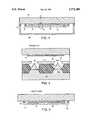
- FIG. 1is a side view of an embodiment of the present invention.
- FIG. 2is a side view of a detailed area of FIG. 1.
- FIG. 3is a side view of an alternative embodiment to the embodiment of the invention seen in FIG. 1.
- a field emission display 1comprising: an anode 10, which in this embodiment comprises a faceplate, or screen of the field emission display.
- This embodimentfurther comprises a phosphor screen 12, located on the anode 10; a cathode 14, attached to anode 10 by glass frit 15; and an evacuated space 16 between the anode 10 and the cathode 14.
- cathode 14 in the region of circle A of FIG. 1comprising: an emitter tip 18 located on the cathode 14 opposite the phosphor screen 12.
- the emitter tip 18comprises an electropositive element 20 both in a body 18a of the emitter tip 18 and on a surface 18b of the emitter tip 18.
- Grid electrode 17Spaced from emitter tip 18 by dielectric 19 is grid electrode 17.
- the distribution of the electropositive element 20 in the body 18a of the emitter tip 18is substantially even.
- the distributionis more uneven, wherein there is a gradient of the electropositive element 20 in the body 18a and the surface 18b is substantially all electropositive element 20.
- the distributionis an exponential change
- the electropositive elementis provided in the body 18a such that the work function of the surface 18b of emitter tip 18 is reduced by at least 50%.
- the work functionis 3.9 eV without an electropositive component, and about 2.0 eV if Na is doped according to the dip process described below.
- Acceptable specific elements for electropositive element 20are chosen from groups IA, IIA, and IIIA of the periodic table.
- One specific element known to be useful as electropositive element 20comprises Cs.
- Another element known to be usefulcomprises Na.
- Others known or believed to be usefulcomprise: H, Li, Be, B, Mg, Al, Ga, Ba, Rb, Ca, K, Sr, and In.
- An example process for manufacturing a field emission display (“FED")comprises the steps of: forming an emitter tip 18 comprising an electropositive element 20 in the body 18a of the emitter tip 18; positioning the emitter tip 18 in opposing relation to a phosphor screen 12 on the display; creating an evacuated space 16 between the emitter tip 18 and the phosphor screen 12; causing the electropositive element 20 to migrate to the emission surface 18b of the emitter tip 18, whereby the display of FIG. 2 results.
- the emitter tip 18is formed by methods that will be understood by those of skill in the art (for example, see U.S. Pat. Nos. 4,940,916; 5,391,259; and 5,229,331, all of which are incorporated herein by reference), and the substrate with the emitter tip 18 is contacted with a solution in a glass container.
- the solutioncomprises an electropositive element as the solute, and a solvent (for example, alcohol).
- solvents believed to be useful according to other embodiments of the inventioninclude: water, acetone, or any other solvent capable of dissolving electropositive salts.
- said electropositive elementcomprises an element chosen from groups IA, IIA, and IIIA of the periodic table.
- One specific element known to be useful as electropositive elementcomprises Cs.
- Others known or believed to be usefulcomprise: H, Li, Be, B, Na, Mg, Al, Ga, Ba, Rb, Ca, K, Sr, and In.
- the contactingcomprises dipping the emitter tip into the solution for a time sufficient to cause 10 m 21 atoms /cm 3 of electropositive material to penetrate into the emitter tip.
- a silicon substrate from which the emitters have been shapedis dipped in a solution of propan-2-ol, as the solvent, and CsCl, the solution being kept just under the boiling temperature.
- a-Siamorphous silicon
- u-Simicro crystalline silicon
- a glass substrate with 7000 angstrom amorphous-silicon emitters formed thereonwas dipped in a solution of propan-1-ol, as the solvent, and NaCl for 15 minutes at a temperature just below boiling.
- the resultwas an approximately 7000 angstrom alpha-silicon/glass structure with Na doped therein.
- SIMS analysis of H, P, and Nawere conducted comparing a similar sample which had not been dipped.
- the NaCl dipped structurehad about 500 times higher Na near the Si surface (at about 500 angstroms depth) then the sample which had not been dipped.
- the Na levelremained higher throughout the 7000 angstroms tested, but decreased to about 80 times higher near the Si/glass interface (at about 6000 angstroms).
- the dipped sampleincluded a slightly higher P than the undipped sample, but the difference was less than about 1.5 times. No H difference was seen between the samples. Mo contamination (due to use of a furnace having therein) was detected on the NaCl dipped sample, but no Mo was seen in the undipped sample. Mo contamination is avoided in other embodiments. Higher K and Ca were also observed in the NaCl dipped sample. Surprisingly, Cl was not detected in either the dipped or undipped sample. This is an important finding as Cl has a high work function and is undesirable in the emitter tip.
- the emitter tipis made after the substrate from which the emitter tip is formed is doped with an electropositive element.
- the substrate on which the emitter tip is manufacturedis dipped, before the formation of the emitter tip, and the emitter tip is then formed on the substrate. According to specific examples of processes believed to be acceptable according to this embodiment, the following parameters are used:
- plasma-enhanced chemical vapor depositionis used to place the electropositive element in the body of the emitter tip.
- the vapor depositionis conducted either before or after the formation of the emitter tip.
- heatingwill cause diffusion of the electropositive element into the body of the emitter tip.
- subsequent heatingcauses the material to migrate to the surface of the emitter tip, where it will not react due to the vacuum, and a low work function emitter tip is thereby achieved.
- Another acceptable method of placement of the electropositive element in the body of the emitter tipis through ion-implantation, again followed by heating after evacuation to cause diffusion.
- the electropositive elementIn embodiments in which the electropositive element is applied before the emitter tip is formed, some of the electropositive element will be exposed during subsequent steps, such as etching. When this occurs, an oxide or non-volatile salt will form, depending upon the atmosphere at the surface of the emitter tip when exposure occurs.
- the oxide or non-volatile salt which is rinsedfor example, with buffered oxide etchant in the case of oxide or water in the case of salt, before further processing.
- Acceptable examples of materials for the substrate which is doped with the electropositive elementinclude, for example, Si, Mo, Cr, and W. Others will occur to those of skill in the art.
- the displayis sealed by glass frit seal 33, chosen to match the thermal expansion characteristic of the cathode 35, which, in this embodiment, comprises a glass substrate 37 on which emitters 39 are formed.
- This embodimentis particularly useful for large area displays.
- the sealingis done in a vacuum space by heating the entire device. The heating to a seal temperature for the frit 33 (for example, 450 degrees C. for a lead-glass-based frit), causes the migration of the electropositive element to the surface of the emitters 39.
- the cathode 14is encased by a backplate 50, which is also sealed in vacuum by a frit 51 by heating.
- a backplate 50which is also sealed in vacuum by a frit 51 by heating.
- the cathode 14comprises a silicon substrate onto which the emitters 18 are formed.
- the cathode 14is attached to faceplate 10 by another frit seal 15, also sealed by heating.
Landscapes
- Engineering & Computer Science (AREA)
- Manufacturing & Machinery (AREA)
- Cathode-Ray Tubes And Fluorescent Screens For Display (AREA)
- Cold Cathode And The Manufacture (AREA)
Abstract
Description
______________________________________ Dip Temperature Solution Composition Dip Time (Degrees C.) ______________________________________ propan-1-ol solvent - NaCl solute 15 minutes 82 methanol solvent - CsCl solute 15 minutes 62 ethanol solvent - NaCl solute 15 minutes 75 methanol solvent NaCl solute 15 minutes 62 propan-1-ol solvent - CsCl solute 15 minutes 82 ehtanol solvent - CsCl solute 15 minutes 75 ______________________________________
______________________________________ Dip Temperature Solution Composition Dip Time (Degrees C.) ______________________________________ propan-1-ol solvent -NaCl solute 15 minutes 82 methanol solvent -CsCl solute 15 minutes 62 ethanol solvent -NaCl solute 15 minutes 75 methanolsolvent NaCl solute 15 minutes 62 propan-1-ol solvent -CsCl solute 15 minutes 82 ethanol solvent -CsCl solute 15 minutes 75 ______________________________________
Claims (14)
Priority Applications (4)
| Application Number | Priority Date | Filing Date | Title |
|---|---|---|---|
| US08/543,819US5772488A (en) | 1995-10-16 | 1995-10-16 | Method of forming a doped field emitter array |
| US09/105,613US6057638A (en) | 1995-10-16 | 1998-06-26 | Low work function emitters and method for production of FED's |
| US09/489,286US7492086B1 (en) | 1995-10-16 | 2000-01-21 | Low work function emitters and method for production of FED's |
| US09/564,356US6515414B1 (en) | 1995-10-16 | 2000-05-01 | Low work function emitters and method for production of fed's |
Applications Claiming Priority (1)
| Application Number | Priority Date | Filing Date | Title |
|---|---|---|---|
| US08/543,819US5772488A (en) | 1995-10-16 | 1995-10-16 | Method of forming a doped field emitter array |
Related Child Applications (1)
| Application Number | Title | Priority Date | Filing Date |
|---|---|---|---|
| US09/105,613DivisionUS6057638A (en) | 1995-10-16 | 1998-06-26 | Low work function emitters and method for production of FED's |
Publications (1)
| Publication Number | Publication Date |
|---|---|
| US5772488Atrue US5772488A (en) | 1998-06-30 |
Family
ID=24169667
Family Applications (4)
| Application Number | Title | Priority Date | Filing Date |
|---|---|---|---|
| US08/543,819Expired - LifetimeUS5772488A (en) | 1995-10-16 | 1995-10-16 | Method of forming a doped field emitter array |
| US09/105,613Expired - Fee RelatedUS6057638A (en) | 1995-10-16 | 1998-06-26 | Low work function emitters and method for production of FED's |
| US09/489,286Expired - Fee RelatedUS7492086B1 (en) | 1995-10-16 | 2000-01-21 | Low work function emitters and method for production of FED's |
| US09/564,356Expired - LifetimeUS6515414B1 (en) | 1995-10-16 | 2000-05-01 | Low work function emitters and method for production of fed's |
Family Applications After (3)
| Application Number | Title | Priority Date | Filing Date |
|---|---|---|---|
| US09/105,613Expired - Fee RelatedUS6057638A (en) | 1995-10-16 | 1998-06-26 | Low work function emitters and method for production of FED's |
| US09/489,286Expired - Fee RelatedUS7492086B1 (en) | 1995-10-16 | 2000-01-21 | Low work function emitters and method for production of FED's |
| US09/564,356Expired - LifetimeUS6515414B1 (en) | 1995-10-16 | 2000-05-01 | Low work function emitters and method for production of fed's |
Country Status (1)
| Country | Link |
|---|---|
| US (4) | US5772488A (en) |
Cited By (8)
| Publication number | Priority date | Publication date | Assignee | Title |
|---|---|---|---|---|
| WO1999044218A1 (en)* | 1998-02-27 | 1999-09-02 | Micron Technology, Inc. | Large-area fed apparatus and method for making same |
| US6004830A (en)* | 1998-02-09 | 1999-12-21 | Advanced Vision Technologies, Inc. | Fabrication process for confined electron field emission device |
| US6045711A (en)* | 1997-12-29 | 2000-04-04 | Industrial Technology Research Institute | Vacuum seal for field emission arrays |
| US20040104658A1 (en)* | 2000-01-14 | 2004-06-03 | Micron Technology, Inc. | Structure and method to enhance field emission in field emitter device |
| US6781319B1 (en)* | 2003-04-11 | 2004-08-24 | Motorola, Inc. | Display and method of manufacture |
| US20080095315A1 (en)* | 2003-01-31 | 2008-04-24 | Cabot Microelectronics Corporation | Method of operating and process for fabricating an electron source |
| USRE40490E1 (en) | 1999-09-02 | 2008-09-09 | Micron Technology, Inc. | Method and apparatus for programmable field emission display |
| US7492086B1 (en) | 1995-10-16 | 2009-02-17 | Micron Technology, Inc. | Low work function emitters and method for production of FED's |
Families Citing this family (4)
| Publication number | Priority date | Publication date | Assignee | Title |
|---|---|---|---|---|
| GB2352315B (en)* | 1999-07-19 | 2003-12-03 | Nokia Mobile Phones Ltd | Sim card reader |
| US20050269286A1 (en)* | 2004-06-08 | 2005-12-08 | Manish Sharma | Method of fabricating a nano-wire |
| KR101299035B1 (en)* | 2006-06-28 | 2013-08-27 | 톰슨 라이센싱 | Liquid crystal display having a field emission backlight |
| US8545599B2 (en)* | 2010-10-28 | 2013-10-01 | Tessera, Inc. | Electrohydrodynamic device components employing solid solutions |
Citations (9)
| Publication number | Priority date | Publication date | Assignee | Title |
|---|---|---|---|---|
| US4325000A (en)* | 1980-04-20 | 1982-04-13 | Burroughs Corporation | Low work function cathode |
| JPH01235124A (en)* | 1988-03-15 | 1989-09-20 | Matsushita Electric Works Ltd | Field emission type electrode |
| US4940916A (en)* | 1987-11-06 | 1990-07-10 | Commissariat A L'energie Atomique | Electron source with micropoint emissive cathodes and display means by cathodoluminescence excited by field emission using said source |
| US5089292A (en)* | 1990-07-20 | 1992-02-18 | Coloray Display Corporation | Field emission cathode array coated with electron work function reducing material, and method |
| US5186670A (en)* | 1992-03-02 | 1993-02-16 | Micron Technology, Inc. | Method to form self-aligned gate structures and focus rings |
| US5210472A (en)* | 1992-04-07 | 1993-05-11 | Micron Technology, Inc. | Flat panel display in which low-voltage row and column address signals control a much pixel activation voltage |
| US5229331A (en)* | 1992-02-14 | 1993-07-20 | Micron Technology, Inc. | Method to form self-aligned gate structures around cold cathode emitter tips using chemical mechanical polishing technology |
| US5358908A (en)* | 1992-02-14 | 1994-10-25 | Micron Technology, Inc. | Method of creating sharp points and other features on the surface of a semiconductor substrate |
| US5391259A (en)* | 1992-05-15 | 1995-02-21 | Micron Technology, Inc. | Method for forming a substantially uniform array of sharp tips |
Family Cites Families (7)
| Publication number | Priority date | Publication date | Assignee | Title |
|---|---|---|---|---|
| US3921022A (en)* | 1974-09-03 | 1975-11-18 | Rca Corp | Field emitting device and method of making same |
| JP2719239B2 (en)* | 1991-02-08 | 1998-02-25 | 工業技術院長 | Field emission device |
| US5449970A (en)* | 1992-03-16 | 1995-09-12 | Microelectronics And Computer Technology Corporation | Diode structure flat panel display |
| US5302238A (en)* | 1992-05-15 | 1994-04-12 | Micron Technology, Inc. | Plasma dry etch to produce atomically sharp asperities useful as cold cathodes |
| US5532177A (en)* | 1993-07-07 | 1996-07-02 | Micron Display Technology | Method for forming electron emitters |
| US5495143A (en)* | 1993-08-12 | 1996-02-27 | Science Applications International Corporation | Gas discharge device having a field emitter array with microscopic emitter elements |
| US5772488A (en) | 1995-10-16 | 1998-06-30 | Micron Display Technology, Inc. | Method of forming a doped field emitter array |
- 1995
- 1995-10-16USUS08/543,819patent/US5772488A/ennot_activeExpired - Lifetime
- 1998
- 1998-06-26USUS09/105,613patent/US6057638A/ennot_activeExpired - Fee Related
- 2000
- 2000-01-21USUS09/489,286patent/US7492086B1/ennot_activeExpired - Fee Related
- 2000-05-01USUS09/564,356patent/US6515414B1/ennot_activeExpired - Lifetime
Patent Citations (10)
| Publication number | Priority date | Publication date | Assignee | Title |
|---|---|---|---|---|
| US4325000A (en)* | 1980-04-20 | 1982-04-13 | Burroughs Corporation | Low work function cathode |
| US4940916A (en)* | 1987-11-06 | 1990-07-10 | Commissariat A L'energie Atomique | Electron source with micropoint emissive cathodes and display means by cathodoluminescence excited by field emission using said source |
| US4940916B1 (en)* | 1987-11-06 | 1996-11-26 | Commissariat Energie Atomique | Electron source with micropoint emissive cathodes and display means by cathodoluminescence excited by field emission using said source |
| JPH01235124A (en)* | 1988-03-15 | 1989-09-20 | Matsushita Electric Works Ltd | Field emission type electrode |
| US5089292A (en)* | 1990-07-20 | 1992-02-18 | Coloray Display Corporation | Field emission cathode array coated with electron work function reducing material, and method |
| US5229331A (en)* | 1992-02-14 | 1993-07-20 | Micron Technology, Inc. | Method to form self-aligned gate structures around cold cathode emitter tips using chemical mechanical polishing technology |
| US5358908A (en)* | 1992-02-14 | 1994-10-25 | Micron Technology, Inc. | Method of creating sharp points and other features on the surface of a semiconductor substrate |
| US5186670A (en)* | 1992-03-02 | 1993-02-16 | Micron Technology, Inc. | Method to form self-aligned gate structures and focus rings |
| US5210472A (en)* | 1992-04-07 | 1993-05-11 | Micron Technology, Inc. | Flat panel display in which low-voltage row and column address signals control a much pixel activation voltage |
| US5391259A (en)* | 1992-05-15 | 1995-02-21 | Micron Technology, Inc. | Method for forming a substantially uniform array of sharp tips |
Non-Patent Citations (13)
| Title |
|---|
| Bauch et al. Apr. 1989 "Effect of Cs Contamination on the Interface State Density of Mnos Capacitors,"Applied Surface Science 39: 356-363. |
| Bauch et al. Apr. 1989 Effect of Cs Contamination on the Interface State Density of Mnos Capacitors, Applied Surface Science 39: 356 363.* |
| Branston et al. Oct. 1991 "Field Emission from Metal-Coated Silicon Tips,"IEEE Transactions on Electron Devices, vol. 38, No. 10, pp. 2329-2333. |
| Branston et al. Oct. 1991 Field Emission from Metal Coated Silicon Tips, IEEE Transactions on Electron Devices, vol. 38, No. 10, pp. 2329 2333.* |
| Ea et al. Jul. 1990 Avalanche Electron Emission Cathode Array, Vacuume Microelectronics Conference.* |
| Evtukh et al. Jul. 30, 1995 "Parameters of the Tip Arrays Covered by Low Work Function Layers," Institute of Semiconductor Physics Academy of Sciences, Prospect Nauki 45, Kiev-252028, Ukraine (Aug. 1995). |
| Evtukh et al. Jul. 30, 1995 Parameters of the Tip Arrays Covered by Low Work Function Layers, Institute of Semiconductor Physics Academy of Sciences, Prospect Nauki 45, Kiev 252028, Ukraine (Aug. 1995).* |
| Evtukh, et al., "Parameters of the Tip Arrays Covered by Low Work Function Layers," J. Vac. Sci. Tech. B 14(3),pp.2130-2134 Pub. May-Jun. 1996). |
| Evtukh, et al., Parameters of the Tip Arrays Covered by Low Work Function Layers, J. Vac. Sci. Tech. B 14(3),pp.2130 2134 Pub. May Jun. 1996).* |
| Macaulay et al. 24 Aug. 1992 "Ceslated thin-film field-emission microcathode arrays," Appl. Phys. Lett., vol. 61, NO. 8, pp. 997-999. |
| Macaulay et al. 24 Aug. 1992 Ceslated thin film field emission microcathode arrays, Appl. Phys. Lett., vol. 61, NO. 8, pp. 997 999.* |
| Michaelson H.B Jan. 1978 "Relation Between an Atomic Electronegativity Scale and the Work Function," IBM J. Res. Develop, vol. 22, No. 1, pp. 72-80. |
| Michaelson H.B Jan. 1978 Relation Between an Atomic Electronegativity Scale and the Work Function, IBM J. Res. Develop, vol. 22, No. 1, pp. 72 80.* |
Cited By (15)
| Publication number | Priority date | Publication date | Assignee | Title |
|---|---|---|---|---|
| US7492086B1 (en) | 1995-10-16 | 2009-02-17 | Micron Technology, Inc. | Low work function emitters and method for production of FED's |
| US6045711A (en)* | 1997-12-29 | 2000-04-04 | Industrial Technology Research Institute | Vacuum seal for field emission arrays |
| US6004830A (en)* | 1998-02-09 | 1999-12-21 | Advanced Vision Technologies, Inc. | Fabrication process for confined electron field emission device |
| US20060189244A1 (en)* | 1998-02-27 | 2006-08-24 | Cathey David A | Method for making large-area FED apparatus |
| US6495956B2 (en) | 1998-02-27 | 2002-12-17 | Micron Technology, Inc. | Large-area FED apparatus and method for making same |
| US20030038588A1 (en)* | 1998-02-27 | 2003-02-27 | Micron Technology, Inc. | Large-area FED apparatus and method for making same |
| US7033238B2 (en) | 1998-02-27 | 2006-04-25 | Micron Technology, Inc. | Method for making large-area FED apparatus |
| WO1999044218A1 (en)* | 1998-02-27 | 1999-09-02 | Micron Technology, Inc. | Large-area fed apparatus and method for making same |
| US7462088B2 (en) | 1998-02-27 | 2008-12-09 | Micron Technology, Inc. | Method for making large-area FED apparatus |
| US6255772B1 (en) | 1998-02-27 | 2001-07-03 | Micron Technology, Inc. | Large-area FED apparatus and method for making same |
| USRE40490E1 (en) | 1999-09-02 | 2008-09-09 | Micron Technology, Inc. | Method and apparatus for programmable field emission display |
| US20040104658A1 (en)* | 2000-01-14 | 2004-06-03 | Micron Technology, Inc. | Structure and method to enhance field emission in field emitter device |
| US20080095315A1 (en)* | 2003-01-31 | 2008-04-24 | Cabot Microelectronics Corporation | Method of operating and process for fabricating an electron source |
| US7875469B2 (en)* | 2003-01-31 | 2011-01-25 | Cabot Microelectronics Corporation | Method of operating and process for fabricating an electron source |
| US6781319B1 (en)* | 2003-04-11 | 2004-08-24 | Motorola, Inc. | Display and method of manufacture |
Also Published As
| Publication number | Publication date |
|---|---|
| US7492086B1 (en) | 2009-02-17 |
| US6057638A (en) | 2000-05-02 |
| US6515414B1 (en) | 2003-02-04 |
Similar Documents
| Publication | Publication Date | Title |
|---|---|---|
| US5772488A (en) | Method of forming a doped field emitter array | |
| US5666025A (en) | Flat-panel display containing structure for enhancing electron emission from carbon-containing cathode | |
| US20010004979A1 (en) | Field emission display and method for fabricating the same | |
| Allen | Field emission from silicon and germanium; field desorption and surface migration | |
| EP0468036A1 (en) | ENCLOSED FIELD EMISSION DEVICE IN ESSENTIAL ORTHOGONAL VAPOR DEPOSITION. | |
| JPH07111869B2 (en) | Method for manufacturing cathode-luminescence display means | |
| Rittner et al. | Studies on the mechanism of operation of the L cathode. I | |
| US4154632A (en) | Method of diffusing aluminum into silicon substrate for manufacturing semiconductor device | |
| Arthur | Gallium arsenide surface structure and reaction kinetics: Field emission microscopy | |
| US5041757A (en) | Sputtered scandate coatings for dispenser cathodes and methods for making same | |
| Baun | Characterization of tungsten impregnated dispenser cathodes using ISS and SIMS | |
| Mroczkowski | Electron emission characteristics of sputtered lanthanum hexaboride | |
| US5065070A (en) | Sputtered scandate coatings for dispenser cathodes | |
| Haas et al. | Thermionic studies of various uranium compounds | |
| US3465196A (en) | Electric discharge device with means to prevent release of occluded gases from the envelope thereof and method | |
| JPH0644893A (en) | Cathode structure | |
| CA1184020A (en) | Method of manufacturing semiconductor device | |
| Lamartine et al. | A model of dispenser cathode activity | |
| US5619091A (en) | Diamond films treated with alkali-halides | |
| Carroll | Scanning-Beam Performance from Negative-Electron-Affinity Activated Silicon Cold Cathode | |
| US3711326A (en) | Promethium sources | |
| Verma | Potential and limitations of caesium iodide as a dynode material for use in electron multipliers | |
| Gotoh et al. | Fabrication of gated niobium nitride field emitter array | |
| Yavas et al. | Pulsed Laser Deposition of Diamond-Like Carbon Films on Gated Si Field Emitter Arrays for Improved Electron Emission | |
| Chopra | Impregnated dispenser M-type cathodes for MW tubes—an overview |
Legal Events
| Date | Code | Title | Description |
|---|---|---|---|
| AS | Assignment | Owner name:MICRON DISPLAY TECHNOLOGY, INC., IDAHO Free format text:ASSIGNMENT OF ASSIGNORS INTEREST;ASSIGNORS:CATHEY, DAVID A.;CHADHA, SURJIT S.;MORADI, BEHNAM;REEL/FRAME:007875/0443;SIGNING DATES FROM 19951002 TO 19951004 | |
| STCF | Information on status: patent grant | Free format text:PATENTED CASE | |
| AS | Assignment | Owner name:MICRON TECHNOLOGY, INC., IDAHO Free format text:MERGER;ASSIGNOR:MICRON DISPLAY TECHNOLOGY, INC.;REEL/FRAME:010859/0379 Effective date:19971216 | |
| FPAY | Fee payment | Year of fee payment:4 | |
| FPAY | Fee payment | Year of fee payment:8 | |
| FPAY | Fee payment | Year of fee payment:12 | |
| AS | Assignment | Owner name:U.S. BANK NATIONAL ASSOCIATION, AS COLLATERAL AGENT, CALIFORNIA Free format text:SECURITY INTEREST;ASSIGNOR:MICRON TECHNOLOGY, INC.;REEL/FRAME:038669/0001 Effective date:20160426 Owner name:U.S. BANK NATIONAL ASSOCIATION, AS COLLATERAL AGEN Free format text:SECURITY INTEREST;ASSIGNOR:MICRON TECHNOLOGY, INC.;REEL/FRAME:038669/0001 Effective date:20160426 | |
| AS | Assignment | Owner name:MORGAN STANLEY SENIOR FUNDING, INC., AS COLLATERAL AGENT, MARYLAND Free format text:PATENT SECURITY AGREEMENT;ASSIGNOR:MICRON TECHNOLOGY, INC.;REEL/FRAME:038954/0001 Effective date:20160426 Owner name:MORGAN STANLEY SENIOR FUNDING, INC., AS COLLATERAL Free format text:PATENT SECURITY AGREEMENT;ASSIGNOR:MICRON TECHNOLOGY, INC.;REEL/FRAME:038954/0001 Effective date:20160426 | |
| AS | Assignment | Owner name:U.S. BANK NATIONAL ASSOCIATION, AS COLLATERAL AGENT, CALIFORNIA Free format text:CORRECTIVE ASSIGNMENT TO CORRECT THE REPLACE ERRONEOUSLY FILED PATENT #7358718 WITH THE CORRECT PATENT #7358178 PREVIOUSLY RECORDED ON REEL 038669 FRAME 0001. ASSIGNOR(S) HEREBY CONFIRMS THE SECURITY INTEREST;ASSIGNOR:MICRON TECHNOLOGY, INC.;REEL/FRAME:043079/0001 Effective date:20160426 Owner name:U.S. BANK NATIONAL ASSOCIATION, AS COLLATERAL AGEN Free format text:CORRECTIVE ASSIGNMENT TO CORRECT THE REPLACE ERRONEOUSLY FILED PATENT #7358718 WITH THE CORRECT PATENT #7358178 PREVIOUSLY RECORDED ON REEL 038669 FRAME 0001. ASSIGNOR(S) HEREBY CONFIRMS THE SECURITY INTEREST;ASSIGNOR:MICRON TECHNOLOGY, INC.;REEL/FRAME:043079/0001 Effective date:20160426 | |
| AS | Assignment | Owner name:JPMORGAN CHASE BANK, N.A., AS COLLATERAL AGENT, ILLINOIS Free format text:SECURITY INTEREST;ASSIGNORS:MICRON TECHNOLOGY, INC.;MICRON SEMICONDUCTOR PRODUCTS, INC.;REEL/FRAME:047540/0001 Effective date:20180703 Owner name:JPMORGAN CHASE BANK, N.A., AS COLLATERAL AGENT, IL Free format text:SECURITY INTEREST;ASSIGNORS:MICRON TECHNOLOGY, INC.;MICRON SEMICONDUCTOR PRODUCTS, INC.;REEL/FRAME:047540/0001 Effective date:20180703 | |
| AS | Assignment | Owner name:MICRON TECHNOLOGY, INC., IDAHO Free format text:RELEASE BY SECURED PARTY;ASSIGNOR:U.S. BANK NATIONAL ASSOCIATION, AS COLLATERAL AGENT;REEL/FRAME:047243/0001 Effective date:20180629 | |
| AS | Assignment | Owner name:MICRON TECHNOLOGY, INC., IDAHO Free format text:RELEASE BY SECURED PARTY;ASSIGNOR:MORGAN STANLEY SENIOR FUNDING, INC., AS COLLATERAL AGENT;REEL/FRAME:050937/0001 Effective date:20190731 | |
| AS | Assignment | Owner name:MICRON SEMICONDUCTOR PRODUCTS, INC., IDAHO Free format text:RELEASE BY SECURED PARTY;ASSIGNOR:JPMORGAN CHASE BANK, N.A., AS COLLATERAL AGENT;REEL/FRAME:051028/0001 Effective date:20190731 Owner name:MICRON TECHNOLOGY, INC., IDAHO Free format text:RELEASE BY SECURED PARTY;ASSIGNOR:JPMORGAN CHASE BANK, N.A., AS COLLATERAL AGENT;REEL/FRAME:051028/0001 Effective date:20190731 |