US5770849A - Smart card device with pager and visual image display - Google Patents
Smart card device with pager and visual image displayDownload PDFInfo
- Publication number
- US5770849A US5770849AUS08/702,087US70208796AUS5770849AUS 5770849 AUS5770849 AUS 5770849AUS 70208796 AUS70208796 AUS 70208796AUS 5770849 AUS5770849 AUS 5770849A
- Authority
- US
- United States
- Prior art keywords
- smart card
- card device
- data
- dimensional array
- image display
- Prior art date
- Legal status (The legal status is an assumption and is not a legal conclusion. Google has not performed a legal analysis and makes no representation as to the accuracy of the status listed.)
- Expired - Lifetime
Links
Images


Classifications
- G—PHYSICS
- G07—CHECKING-DEVICES
- G07F—COIN-FREED OR LIKE APPARATUS
- G07F7/00—Mechanisms actuated by objects other than coins to free or to actuate vending, hiring, coin or paper currency dispensing or refunding apparatus
- G07F7/08—Mechanisms actuated by objects other than coins to free or to actuate vending, hiring, coin or paper currency dispensing or refunding apparatus by coded identity card or credit card or other personal identification means
- G07F7/10—Mechanisms actuated by objects other than coins to free or to actuate vending, hiring, coin or paper currency dispensing or refunding apparatus by coded identity card or credit card or other personal identification means together with a coded signal, e.g. in the form of personal identification information, like personal identification number [PIN] or biometric data
- G07F7/1008—Active credit-cards provided with means to personalise their use, e.g. with PIN-introduction/comparison system
- G—PHYSICS
- G06—COMPUTING OR CALCULATING; COUNTING
- G06K—GRAPHICAL DATA READING; PRESENTATION OF DATA; RECORD CARRIERS; HANDLING RECORD CARRIERS
- G06K7/00—Methods or arrangements for sensing record carriers, e.g. for reading patterns
- G06K7/0013—Methods or arrangements for sensing record carriers, e.g. for reading patterns by galvanic contacts, e.g. card connectors for ISO-7816 compliant smart cards or memory cards, e.g. SD card readers
- G—PHYSICS
- G06—COMPUTING OR CALCULATING; COUNTING
- G06Q—INFORMATION AND COMMUNICATION TECHNOLOGY [ICT] SPECIALLY ADAPTED FOR ADMINISTRATIVE, COMMERCIAL, FINANCIAL, MANAGERIAL OR SUPERVISORY PURPOSES; SYSTEMS OR METHODS SPECIALLY ADAPTED FOR ADMINISTRATIVE, COMMERCIAL, FINANCIAL, MANAGERIAL OR SUPERVISORY PURPOSES, NOT OTHERWISE PROVIDED FOR
- G06Q20/00—Payment architectures, schemes or protocols
- G06Q20/30—Payment architectures, schemes or protocols characterised by the use of specific devices or networks
- G06Q20/34—Payment architectures, schemes or protocols characterised by the use of specific devices or networks using cards, e.g. integrated circuit [IC] cards or magnetic cards
- G06Q20/341—Active cards, i.e. cards including their own processing means, e.g. including an IC or chip
- G—PHYSICS
- G07—CHECKING-DEVICES
- G07F—COIN-FREED OR LIKE APPARATUS
- G07F7/00—Mechanisms actuated by objects other than coins to free or to actuate vending, hiring, coin or paper currency dispensing or refunding apparatus
- G07F7/08—Mechanisms actuated by objects other than coins to free or to actuate vending, hiring, coin or paper currency dispensing or refunding apparatus by coded identity card or credit card or other personal identification means
- G07F7/0873—Details of the card reader
- G07F7/088—Details of the card reader the card reader being part of the point of sale [POS] terminal or electronic cash register [ECR] itself
- G07F7/0886—Details of the card reader the card reader being part of the point of sale [POS] terminal or electronic cash register [ECR] itself the card reader being portable for interacting with a POS or ECR in realizing a payment transaction
Definitions
- the present inventionpertains, generally, to portable smart card devices and, more particularly, to a portable smart card device including a communications transceiver and a visual display.
- Smart cardsare becoming very popular around the world.
- a smart cardis defined as a card (similar in size to a common credit card) containing a semiconductor chip with some electronics and a memory for storing information.
- Smart cardsare used to store personal information, ranging from medical information to financial data, as well as the storage of monetary value.
- the large amount of information, or data, stored on a smart cardis not generally accessible or capable of editing or use without the intervention of a smart card device, that is capable of being interfaced with the smart card.
- various different smart cardsare presently in use, including those that operate at a variety of different voltages and those that can be accessed by electrical contacts, contactless cards, optically readable cards, magnetically readable cards, etc. It is desirable, therefore, to provide means whereby the owner can view the stored information on the card to determine the status as well as providing means for the conducting of commercial and financial transactions utilizing the smart card.
- a smart card deviceincluding a portable housing with a viewing aperture and a visual image display, such as a virtual image display, positioned in the housing to provide an image for viewing at the viewing aperture.
- the visual image displayalso includes a data input terminal designed to receive image data thereon.
- a sensor structureis mounted in the housing and constructed to have a smart card with data stored thereon positioned adjacent thereto in data sensing juxtaposition.
- the sensor structureincludes an input terminal for receiving data thereon and an output terminal having sensed data thereon.
- the smart card device of the present inventionfurther includes a transceiver mounted in the housing and connected to the electronics for receiving and transmitting data between the electronics of the portable smart card device and the host database.
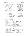
- FIG. 1is an isometric view of a portable smart card device in accordance with the present invention
- FIG. 2is a simplified sectional view as seen along the line 2--2 of FIG. 1;
- FIG. 3is a simplified schematic view of a portion of the portable smart card device of FIG. 1;
- FIG. 4is a simplified block diagram of a portion of the portable smart card device of FIG. 1;
- FIG. 5is a view in top plan of a portion of the apparatus of FIG. 4;
- FIGS. 6, 7 and 8are top front and side views of a portion of the portable smart card device of FIG. 1;
- FIG. 9is an enlarged side view of the apparatus of FIG. 6;
- FIG. 10is a block diagram of another visual display for the portable smart card device of FIG. 1;
- FIG. 11is an isometric illustrating the operation of the portable smart card device of FIG. 1;
- FIG. 12is a block diagram of the portable smart card device of FIG. 1.
- FIGS. 1 and 2illustrate a specific embodiment of a smart card device 10 in accordance with the present invention.
- Smart card device 10includes a portable housing 11 which is ergonomically designed to be handheld, that is, housing 11 is formed to conveniently fit the hand and allow comfortable use of a plurality of controls 19 to operate the device.
- Housing 11also includes a slot 12 for receiving a smart card 13 therein and allowing the sensing of information stored on smart card 13.
- Slot 12is designed to place smart card 13 adjacent to sensor structure 15 mounted in housing 11 in data sensing juxtaposition. It will of course be understood that while slot 12 is preferable for correctly positioning smart card 13, other structures might be utilized, including simply placing smart card 13 adjacent to a sensor structure that is externally accessible.
- Housing 11also has a visual display 14 mounted therein for providing a visual image of the information stored on smart card 13 and information pertaining to transactions performed utilizing smart card device 10 and communications with a host database (discussed presently).
- Electronics 16are mounted in housing 11 in electrical communication with sensor structure 15 and a communications transceiver 17, which in this specific embodiment are illustrated as being mounted directly on a circuit board containing and interconnecting electronics 16, sensor structure 15, and communications transceiver 17.
- the circuit board containing electronics 16is also positioned to have mounted thereon and electrically connected to electronics 16, apparatus 20 including a two dimensional array of light emitting devices connected to provide a complete real image in visual display 14.
- electronics 16include a central processing unit (CPU) and memory (RAM or ROM) capable of working with the CPU and visual display 14.
- sensor structure 15is constructed to physically engage external electrical contacts on smart card 13 so that smart card 13 is directly connected to the CPU in electronics 16.
- the CPUis programmed to interface with the memory and circuitry on smart card 13 and provide the information stored on smart card 13 to visual display 14 in the form of image data. Visual display 14 then generates an image (or images) of the sensed data from smart card 13.
- sensor structure 15can include optical sensors, capable of sensing optically stored information, magnetic sensors, capable of sensing magnetically stored information, and/or electronic sensors, capable of sensing electronically stored information, in addition to or instead of physically engaging electrical contacts.
- the CPU in electronics 16is programmed to interface with communications transceiver 17 and provide for transmissions to and from smart card device 10, thus sensor structure 15 is constructed to communicate information to smart card 13 from the CPU, as well as communicating information from smart card 13 to the CPU.
- smart card device 10uses cryptological calculations, making data transmissions secure.
- security informationsuch as a PIN code, which could be input as a series of unique numbers or letters in visual display 14 using controls 19, or as a biometric identifier, such as a finger print or retinal scan.
- the display element 14when fabricated as a high resolution touch sensitive panel, is capable of not only displaying data but also acting as the biometric input device for more secure applications.
- the smart card CPUprocesses the security information and using communications transceiver 17, transmits a transaction packet, dependent upon user input, to a host financial database.
- the transaction packet once received by the host databaseis verified and processed by the host database, transmitting confirmation back to smart card device 10, which subsequently records the information on smart card 13 and provides a visual image thereof.
- a central processing unitCPU
- CPUcentral processing unit
- the transmission of information from smart card device 10 to the host databaseutilizes wireless technology, more specifically communications transceiver 17, such as a two-way pager device, capable of transmitting and receiving the information utilized during the transaction.
- communications transceiver 17such as a two-way pager device, capable of transmitting and receiving the information utilized during the transaction.
- speaker/microphone 18is provided within housing 11 of smart card device 10 a speaker/microphone 18 as part of communications transceiver 17.
- smart card device 10as a conventional pager device is anticipated by this disclosure.
- controls 19allow the user to choose the mode of operation of device 10, more specifically choosing between a smart card reader/transmission mode or in a conventional pager mode.
- smart card device 10is programmed to permit use as a conventional pager as a default when a smart card, such as smart card 13, is not physically engaged in slot 12.
- smart card device 10is capable of conducting transactions allowing for remote transactions, such as the addition of monetary value to value holding smart cards as well as the purchase, thus subsequent debit from a value card, such as for the purchase of catalog sales merchandise.
- remote transactionssuch as the addition of monetary value to value holding smart cards as well as the purchase
- a value cardsuch as for the purchase of catalog sales merchandise.
- the userwould be able to receive and preview specially formatted graphical advertisements within display 14, such as for a movie theatre.
- the userwould conduct a transaction for the purchase of movie tickets by transferring money from an inserted stored value card.
- the ticket purchase informationwould be transmitted form the host database and ultimately stored on the smart card. Once arriving at a movie theatre location, the user would then produce the card holding the purchased ticket information.
- the combination of communications transceiver 17 to smart card device 10makes it possible to access a wide variety of interactive graphical consumer data.
- Display 14includes apparatus 20 for providing an image on a surface 23.
- An optical system, represented by lens 24,is positioned in spaced relation to surface 23 of apparatus 20 and produces a virtual image viewable by an eye spaced from an aperture 25 defined by lens 24.
- Apparatus 20is illustrated in more detail in FIG. 4 and includes, for example, semiconductor electronics such as a light emitting device (LED) array 26 driven by data processing circuits 27.
- Data processing circuits 27include, for example, logic and switching circuit arrays for controlling each LED in LED array 26.
- Data processing circuits 27include, in addition to or instead of the logic and switching arrays, a microprocessor or similar circuitry for processing input signals of software instructions to produce a desired image on a device such as LED array 26. It will be understood that data processing circuits 27 and LED array 26, while illustrated separately for purposes of this description, could be formed on the same semiconductor chip in some applications.
- LED array 26includes light emitting diodes which are utilized because of the extremely small size that can be achieved and because of the simplicity of construction and operation. It will of course be understood that other image generating devices may be utilized, including but not limited to lasers (such as vertical cavity surface emitting lasers), liquid crystal devices, organic light emitting diodes, etc.
- FIG. 5a plan view of LED array 26 is illustrated in which the LEDs are formed in a regular pattern of rows and columns on a single substrate 29, which in this embodiment is a semiconductor chip. Portions of substrate 29 are broken away to simplify the drawing but it should be understood that many of the other circuits, and especially drivers, could be included on the same substrate.
- the specific LEDsare energized to produce an image or images.
- Digital or analog datais received at input terminal 28 and converted by data processing circuits 27 into signals capable of energizing selected LEDs to generate the predetermined image.
- LED array 26 and substrate 29are greatly enlarged in the figures.
- the actual size of substrate 29is on the order of a few milli-meters along each side, with the light emitting area or array being generally in the range of 2 to 50 milli-meters and preferably 5 to 10 milli-meters, with each LED being less than 20 microns on each side and preferably on the order of as little as one micron on a side. It should be understood that the actual light emitting device array is much smaller, because bonding pads, etc. add several milli-meters of area on each side. Generally, the larger size substrates or chips simply mean that more light emitting devices are used in the array to provide more definition, color, etc.
- the lens systemrepresented schematically by lens 24, is mounted in spaced relation from surface 23 of apparatus 20 so as to receive the image from surface 23, magnify it a predetermined amount and create the aperture within which the virtual image is viewed.
- lens 24magnifies the image fifteen times (15 ⁇ ) so that the image from LED array 26 is magnified fifteen times its original angular size.
- a magnification of at least tenis required to magnify the image sufficiently to be perceived by a human eye.
- the lens systemmay be adjustable for focus and additional magnification, if desired, or may be fixed in housing 11 for simplicity.
- FIGS. 6, 7 and 8illustrate a top plan view, front view, and side elevation, respectively, of a miniature virtual image display 30 which, in a preferred embodiment, is used as visual display 14 in smart card device 10.
- Miniature virtual image display 30incorporates a single fold optical magnifier 32.
- FIGS. 6, 7 and 8illustrate miniature virtual image display 30 approximately the actual size to provide some indication as to the extent of the reduction in size achieved by the apparatus.
- Display 30includes image generating apparatus 35 with an array of light emitting devices, such as organic or inorganic light emitting diodes, field emission devices, vertical cavity surface emitting lasers, liquid crystal devices, etc.
- image generating apparatus 35includes an array of light emitting devices, more specifically an array containing 240 columns and 144 rows of light emitting devices.
- Each light emitting deviceis fabricated approximately 20 microns on a side with a center-to-center spacing between adjacent devices of no more than 20 microns. Each light emitting device is turned ON with approximately 1.8 volts and utilizes approximately 50 ⁇ A of current when it is turned ON. Apparatus 35 produces a luminance less than approximately 15 fL. Apparatus 35 is mounted on the under-surface of a glass substrate 36 and a driver board 38 is bump-bonded to substrate 36. Additional information on driver boards and bonding of substrates to the driver boards is disclosed in U.S. Pat. No. 5,432,358, entitled "INTEGRATED ELECTRO-OPTICAL PACKAGE", issued Jul. 11, 1995 and assigned to the same assignee, which information is included herein by reference.
- Single fold optical magnifier 32is also mounted on substrate 36 and includes a plurality of optical elements defining a light path from apparatus 35 to a viewing aperture 39, best seen in FIG. 7.
- the plurality of optical elementsare constructed to angularly magnify images, generated by apparatus 35, at a light inlet of a first optical element by greater than ten. Because of the length of the optical path and the size of apparatus 35 (the image source), the horizontal field of view of the optics ranges from approximately 11 degrees at a magnification of 10 ⁇ to 22 degrees at a magnification of 20 ⁇ , with the present embodiment having a horizontal field of view of approximately 16 degrees and a magnification of 15 ⁇ .
- the plurality of optical elementsincludes a first optical element 40 having a field flattening light inlet 42, a spheric surface serving as a light outlet 43 and directed at an angle to field flattening light inlet 42 and a reflecting surface 45 optically positioned between field flattening light inlet 42 and light outlet 43 so as to direct light from field flattening light inlet 42 to light outlet 43.
- element 40is formed as a prism and is molded from an optical quality plastic.
- optical quality plasticis material having a high index of refraction, between approximately 1.5 and 1.6.
- Reflecting surface 45may be a separate silvered mirror that is simply molded into first optical element 40, or reflecting surface 45 can be silvered after formation of first optical element 40, or reflecting surface 45 can be uncoated and used in a total internal reflection mode.
- field flattening light inlet 42takes the form of an aspheric field flattening concave surface molded directly into first optical element 40 and formed as an integral part thereof. It will be understood, however, that field flattening light inlet 42 could be formed as a separate lens and subsequently positioned in optical alignment with the lower surface of first optical element 40. Separate components of course result in additional components and assembly steps which can increase the cost and size of the final structure.
- Reflecting surface 45is disposed, with respect to field flattening light inlet 42 and light outlet 43, to fold or bend light passing through first optical element 40 at an angle between approximately 80° to 100°. More specifically, in the embodiment illustrated, light is reflected at an angle of approximately 95°. It has been found, for example, that an angle of 95° avoids vignetting on the lower part of the image at the outlet of single fold optical magnifier 32.
- a significant part of the design of miniature virtual image display 30is the use of a solid, single fold prism with a convex outlet face to enable increased angular magnification (reduced effective focal length) in the same volume of space compared to the use of a simple turning mirror in the air.
- the plurality of optical elementsfurther includes an optical lens 47 having a light inlet 48, positioned adjacent light outlet 43 of first optical element 40, and a light outlet 49.
- optical lens 47is a biaspheric optical lens having an aspheric surface defining light inlet 48 and an aspheric surface defining light outlet 49.
- Optical lens 47is fixedly mounted relative to first optical element 40 by any convenient means including an outer housing (illustrated schematically in FIGS. 6-8), a mounting frame, or any other convenient structure.
- the aspheric surfacesincluding light outlet 49 and light inlet 48 of optical lens 47 and light outlet 43 and field flattening light inlet 42 of first optical element 40 are designed to reduce and/or eliminate any aberration in wavefront as it passes from field flattening light inlet 42 to light outlet 49 of optical lens 47.
- the plurality of optical elementsdefine a light path from field flattening light inlet 42 of first optical element 40 to light outlet 49 of optical lens 47.
- the total average optical length of the optical pathshould be in the range of approximately 15 to 35 millimeters.
- the optical path from field flattening light inlet 42 to the aspheric surface defining light outlet 49 of optical lens 47is approximately 20 millimeters.
- the plurality of optical elementsare constructed to include at least one diffractive optical element positioned in the light path so as to provide additional, primarily chromatic (in this embodiment), aberration correction.
- a diffractive optical element 50is incorporated into the aspheric surface defining light inlet 48 of optical lens 47. It will of course be understood that diffractive optical elements can, instead of, or in addition to diffractive optical element 50, can be included in any other surface of the plurality of elements in miniature virtual image display 30.
- a diffractive optical elementis included in a surface that is substantially normal to the light path, as opposed to those in which the light strikes the surface at an angle, the diffractive optical element is somewhat easier to construct because of rotational symmetry, whereas surfaces on which light strikes at an angle have nonrotational symmetry. Because the aspheric surfaces and diffractive optical element 50 make optical lens 47 relatively complex, it has been found that fabrication of optical lens 47 is best done by injection molding.
- first optical element 40 and optical lens 47can be constructed to form a complete magnifier
- a low power optical lens 51is included as an example of possible extensions of the magnifier.
- Low power optical lens 51includes a spheric surface which defines a light input 52 and a spheric surface which defines a light output 53.
- a diffractive optical element 54is formed in the inlet surface of low power optical lens 51 to provide additional aberration correction.
- Low power optical lens 51is mounted adjacent optical lens 47 and forms an outlet optical element that defines an aperture through which the angularly magnified image can be viewed.
- low power optical lens 51may add somewhat to the size and complexity of miniature virtual image display 30, but provides some angular magnification and aberration correction that reduces the complexity of the various other elements, which can in many applications reduce the overall cost of display 30. Because of its low power, low power optical lens 51 may also be used as the package window, or viewing aperture. In applications in which only first optical element 40 and optical lens 47 are utilized, it may be convenient to define the viewing aperture with a glass or plastic window, which may be clear, a light filter, etc.
- first optical element 40(and other elements 47 and 51, if desired) is mounted on substrate 36 by means of a threaded adjustment 56 which can be rotated by a thumb screw, screwdriver, etc., to move the fixed assembly of elements 40, 47 and 51 vertically toward and away from substrate 36 and apparatus 35. Focusing is accomplished by simply changing the distance between field flattening light inlet 42 and the image generated on apparatus 35.
- FIG. 10is a block diagram of a direct retinal scan display, which might also be utilized as visual display 14 of FIG. 2.
- a laser 60which may be any of the well known lasers including solid state lasers, such as vertical cavity surface emitting lasers, diode lasers, diode-pumped lasers, etc., supplies a coherent light beam to a modulator 62.
- Modulator 62impresses video information onto the light beam generally by modulating the intensity of the light beam as, for example, by providing changes in the power level of laser 60.
- the modulationcould be as simple as turning laser 60 off and on, which essentially translates into a digital system.
- Acousto-optic modulatorsare one of the preferred modulators for most applications, but other techniques, such as electro-optics and mechanical are completely feasible.
- the modulated light beam from modulator 62is directed to a deflection system 63.
- a lens system 64is used to focus the light beam from deflection system 63 into an eye.
- the focal length of lens system 64is chosen so that the scanning system focal point is within the pupil of the eye and the coherent beam focal point is at the retina of the eye.
- Timing and control of modulator 62 and deflection system 63is provided by electronics 65.
- Electronics 65includes a basic oscillator, or timer, which provides the timing signals to cause the sweeping and modulating to occur at the proper times.
- electronics 65provides video signals to modulator 62 to modulate the light beam to the correct intensity at the required times.
- electronics 65provides horizontal and vertical (orthogonal) deflection signals to cause deflection system 63 to periodically scan the light beam in a raster.
- the horizontal deflection frequencymay be on the order of 15 to 30 kHz.
- the vertical deflectionis on the order of 60 Hz.
- the modulating frequencymay be on the order of 12 MHz.
- deflection system 63The purpose of deflection system 63 is to scan the modulated light beam on the retina of the eye, or "write" an image on the retina.
- deflection system 63 and lens system 64There are many possible configurations for deflection system 63 and lens system 64, depending upon the application of the display and how it is desired to form the image in the eye. Additional information on this type of display is available in a copending U.S. patent application entitled “DIRECT RETINAL SCAN DISPLAY", Ser. No. 08/292,193, filed Aug. 18, 1994, assigned to the same assignee, which is a file wrapper continuation of U.S. patent application entitled “DIRECT RETINAL SCAN DISPLAY", Ser. No. 07/857,193, filed Mar. 24, 1992. While the direct retinal scan display does not technically generate a virtual image, the direct retinal scan display is included in the definition of a virtual display apparatus for purposes of this disclosure because of the similarity thereto.
- FIG. 11a perspective view of smart card device 10 is illustrated with miniature virtual image display 30 mounted therein so that only viewing aperture 39 is visible. It is anticipated by this disclosure, that dependent upon the use requirements of device 10, there may be included within housing 11 a direct view display (not shown) for the viewing of a direct view image, such as in the instance where device 10 is being utilized simply as a conventional paging unit.
- FIG. 11further illustrates a typical view 70, or virtual image, of the information stored on smart card 13, as well as transaction information, as seen by an operator looking into viewing aperture 39 of smart card device 10, which view 70 (virtual image) appears to be behind smart card device 10.
- View 70could appear to be as large as an 8.5 by 11 sheet of paper or larger and could include, for example, a complete financial statement of previous account activity, or simply informational data regarding the current transaction, etc.
- FIG. 12a simplified block diagram of smart card device 10 is illustrated.
- a central processor unit (CPU) 75is illustrated as a part of electronics 16, using a random access memory (RAM) 76 and a read only memory (ROM) 77.
- RAMrandom access memory
- ROMread only memory
- an MC68HC05SC21 available commercially from MOTOROLA, INC.is utilized as CPU 75.
- RAM 76 and ROM 77can be internal to CPU 75 and/or external memories can be provided for additional or specialized features.
- a power management circuit 80is provided to accommodate different smart cards with different power and/or different voltage requirements (e.g. voltages in a range of 1 to 12 volts).
- a card interface 82is used to couple the smart card to CPU 75 and, as described previously, may include any or all of electrical contacts for direct physical connection, optical readers, magnetic sensors, electronic sensors (e.g. infrared sensors, RF sensors, etc. for contactless cards).
- card interface 82includes sensor structure 15 (FIG. 2) including data input and output terminals 83.
- a user interface 85is provided to allow the user to communicate with CPU 75 and, ultimately, the smart card.
- User interface 85includes various buttons and controls for operating visual display 14 (in this embodiment).
- user interface 85includes at least an OFF/ON control and means, such as a cursor for pull-down menus, advance/reverse images, etc., to control the views being generated by visual display 14.
- a security circuit 86which generally will allow operation of smart card device 10 only in response to some secret information known only to the smart card owner, e.g. a PIN number, biometric input, some internal circuit that matches an internal circuit of the smart card, etc. as well as the completion of specific transactions in response to verification of security information by the host database.
- user interface 85may include one or more buttons (generally similar to controls 19 of FIG. 1) which must be properly operated by the user to activate smart card device 10.
- a visual display 90includes an array of light emitting devices coupled to driver circuits 92, RAM 93 for storing and/or correctly orienting image data supplied by CPU 75 and data input terminal 94.
- visual display 90can be any of the displays described above and preferably is miniature virtual image display 30 (FIGS. 6-9).
- visual display 90can include an LCD array such as that described in U.S. Pat. No. 5,486,946, entitled "INTEGRATED ELECTRO-OPTIC PACKAGE FOR REFLECTIVE SPATIAL LIGHT MODULATORS", issued Jan. 23, 1996 and assigned to the same assignee.
- some typical electronics for generating an image on an array of light emitting devicesis described in U.S. Pat. No.
- a communications transceiver 95such as a two-way pager, or the like, including a data input/output terminal 97, communicates with a host database 96 to transact business between smart card device 10 and the host database 96.
- new and improved apparatusfor viewing information and conducting specific transactions utilizing a smart card.
- the new and improved apparatuscan be standardized to receive virtually any of the multiple types of smart cards and contains safe features to prevent unwarranted viewing of the information.
- the new and improved apparatusis portable and easy to operate so that each smart card owner can easily carry an apparatus with them, if they desire, or have one at home or the office for instant apprisal of information stored on the smart card as well as the conduction of commercial and/or financial transactions utilizing the smart card.
Landscapes
- Engineering & Computer Science (AREA)
- General Physics & Mathematics (AREA)
- Physics & Mathematics (AREA)
- Business, Economics & Management (AREA)
- Theoretical Computer Science (AREA)
- General Business, Economics & Management (AREA)
- Accounting & Taxation (AREA)
- Strategic Management (AREA)
- Computer Networks & Wireless Communication (AREA)
- Microelectronics & Electronic Packaging (AREA)
- Artificial Intelligence (AREA)
- Computer Vision & Pattern Recognition (AREA)
- Devices For Indicating Variable Information By Combining Individual Elements (AREA)
- Control Of Vending Devices And Auxiliary Devices For Vending Devices (AREA)
- Mobile Radio Communication Systems (AREA)
- Telephonic Communication Services (AREA)
- Control Of Indicators Other Than Cathode Ray Tubes (AREA)
Abstract
Description
Claims (25)
Priority Applications (5)
| Application Number | Priority Date | Filing Date | Title |
|---|---|---|---|
| US08/702,087US5770849A (en) | 1996-08-23 | 1996-08-23 | Smart card device with pager and visual image display |
| EP97114066AEP0825546A3 (en) | 1996-08-23 | 1997-08-14 | Smart card device with pager and visual image display |
| KR1019970039871AKR19980018848A (en) | 1996-08-23 | 1997-08-21 | Smart card device with pager and visual image display |
| JP9241805AJPH10187904A (en) | 1996-08-23 | 1997-08-22 | Smart card device with pager and visual image display |
| CN97117654ACN1176439A (en) | 1996-08-23 | 1997-08-22 | Smart card device with pager and visual image display |
Applications Claiming Priority (1)
| Application Number | Priority Date | Filing Date | Title |
|---|---|---|---|
| US08/702,087US5770849A (en) | 1996-08-23 | 1996-08-23 | Smart card device with pager and visual image display |
Publications (1)
| Publication Number | Publication Date |
|---|---|
| US5770849Atrue US5770849A (en) | 1998-06-23 |
Family
ID=24819820
Family Applications (1)
| Application Number | Title | Priority Date | Filing Date |
|---|---|---|---|
| US08/702,087Expired - LifetimeUS5770849A (en) | 1996-08-23 | 1996-08-23 | Smart card device with pager and visual image display |
Country Status (5)
| Country | Link |
|---|---|
| US (1) | US5770849A (en) |
| EP (1) | EP0825546A3 (en) |
| JP (1) | JPH10187904A (en) |
| KR (1) | KR19980018848A (en) |
| CN (1) | CN1176439A (en) |
Cited By (126)
| Publication number | Priority date | Publication date | Assignee | Title |
|---|---|---|---|---|
| US6003135A (en)* | 1997-06-04 | 1999-12-14 | Spyrus, Inc. | Modular security device |
| US6019284A (en)* | 1998-01-27 | 2000-02-01 | Viztec Inc. | Flexible chip card with display |
| US6068183A (en)* | 1998-04-17 | 2000-05-30 | Viztec Inc. | Chip card system |
| US6088802A (en)* | 1997-06-04 | 2000-07-11 | Spyrus, Inc. | Peripheral device with integrated security functionality |
| US6216015B1 (en) | 1999-02-04 | 2001-04-10 | Motorola, Inc. | Wireless subscriber unit and method for managing smart card data |
| US6243689B1 (en)* | 1998-12-29 | 2001-06-05 | Robert G. Norton | System and method for authorizing electronic funds transfer at a point of sale |
| US6315195B1 (en)* | 1998-04-17 | 2001-11-13 | Diebold, Incorporated | Transaction apparatus and method |
| US20020019811A1 (en)* | 2000-05-31 | 2002-02-14 | Veristar Corporation | Biometric financial transaction system and method |
| US20020029254A1 (en)* | 2000-09-06 | 2002-03-07 | Davis Terry L. | Method and system for managing personal information |
| WO2002029703A1 (en)* | 2000-10-06 | 2002-04-11 | Dieceland Technologies Corp. | Electronic movie card |
| US20020054078A1 (en)* | 2000-06-13 | 2002-05-09 | Yoshinori Taniwaki | Audience information collecting system, audience information collecting method, and information providing method |
| US6394343B1 (en)* | 1999-10-14 | 2002-05-28 | Jon N. Berg | System for card to card transfer of monetary values |
| US6404862B1 (en)* | 1998-05-29 | 2002-06-11 | International Computers Limited | Authentication device |
| US20020128977A1 (en)* | 2000-09-12 | 2002-09-12 | Anant Nambiar | Microchip-enabled online transaction system |
| US6450407B1 (en) | 1998-04-17 | 2002-09-17 | Viztec, Inc. | Chip card rebate system |
| US6484260B1 (en)* | 1998-04-24 | 2002-11-19 | Identix, Inc. | Personal identification system |
| US6490443B1 (en) | 1999-09-02 | 2002-12-03 | Automated Business Companies | Communication and proximity authorization systems |
| US20030028435A1 (en)* | 2000-06-28 | 2003-02-06 | Joel Gaillard | System and method for deferred purchase of a product |
| US20030080852A1 (en)* | 2001-10-31 | 2003-05-01 | International Business Machines Corporation | Secure smart card |
| US20030135462A1 (en)* | 1998-11-17 | 2003-07-17 | Brake Francis B. | Customer activated multi-value (CAM) card |
| US20030141963A1 (en)* | 2000-02-15 | 2003-07-31 | Urs Furter | Transponder device for the identification of objects in front of pieces of equipment |
| US6631849B2 (en) | 2000-12-06 | 2003-10-14 | Bank One, Delaware, National Association | Selectable multi-purpose card |
| US20040044961A1 (en)* | 2002-08-28 | 2004-03-04 | Leonid Pesenson | Method and system for transformation of an extensible markup language document |
| US20040056087A1 (en)* | 2002-09-20 | 2004-03-25 | Bonneau Walter C. | Dynamic smart card/media imaging |
| US20040059675A1 (en)* | 2001-03-16 | 2004-03-25 | Joel Gaillard | System and method for replacing identification data on a portable transaction device |
| US20040171406A1 (en)* | 2003-02-28 | 2004-09-02 | Gary Purk | Transaction card providing displayed information |
| US20040188519A1 (en)* | 2003-03-31 | 2004-09-30 | Kepler, Ltd. A Hong Kong Corporation | Personal biometric authentication and authorization device |
| US20050029349A1 (en)* | 2001-04-26 | 2005-02-10 | Mcgregor Christopher M. | Bio-metric smart card, bio-metric smart card reader, and method of use |
| US20050144133A1 (en)* | 1994-11-28 | 2005-06-30 | Ned Hoffman | System and method for processing tokenless biometric electronic transmissions using an electronic rule module clearinghouse |
| US20050154663A1 (en)* | 1999-06-04 | 2005-07-14 | First Usa Bank, N.A. | System and method for card processing with automated payment of club, merchant, and service provider fees |
| US6920437B2 (en) | 1996-07-15 | 2005-07-19 | Intelli-Check, Inc. | Authentication system for identification documents |
| US20050168340A1 (en)* | 2002-03-18 | 2005-08-04 | Mosher Walter W.Jr. | Enhanced identification appliance having a plurality or data sets for authentication |
| US6931538B1 (en)* | 1999-09-24 | 2005-08-16 | Takashi Sawaguchi | Portable personal authentication apparatus and electronic system to which access is permitted by the same |
| US6934664B1 (en) | 2002-05-20 | 2005-08-23 | Palm, Inc. | System and method for monitoring a security state of an electronic device |
| US20050263596A1 (en)* | 2004-05-12 | 2005-12-01 | Solicore, Inc. | Portable charger, including portable sleeve, for an electronically readable card |
| US7040533B1 (en) | 1998-04-17 | 2006-05-09 | Diebold, Incorporated | Cash withdrawal from ATM via videophone |
| US7051925B2 (en) | 2001-08-13 | 2006-05-30 | Bankone Delaware, N.A. | System and method for funding a collective account by use of an electronic tag |
| US20060165236A1 (en)* | 2005-01-27 | 2006-07-27 | Research In Motion Limited, A Canadian Corporation | Wireless personal area network having authentication and associated methods |
| US7086586B1 (en) | 2003-08-13 | 2006-08-08 | Bank One, Delaware, National Association | System and method for a card payment program providing mutual benefits to card issuers and cardholders based on financial performance |
| US7130828B2 (en) | 1998-06-22 | 2006-10-31 | Jpmorgan Chase Bank, N.A. | Debit purchasing of stored value card for use by and/or delivery to others |
| US7165049B2 (en) | 2000-02-09 | 2007-01-16 | Jpmorgan Chase Bank, N.A. | Sponsor funded stored value card |
| US7181017B1 (en) | 2001-03-23 | 2007-02-20 | David Felsher | System and method for secure three-party communications |
| US7207477B1 (en) | 2004-03-08 | 2007-04-24 | Diebold, Incorporated | Wireless transfer of account data and signature from hand-held device to electronic check generator |
| US7260549B2 (en) | 2000-04-07 | 2007-08-21 | Jpmorgan Chase Bank, N.A. | Method and system for managing risk |
| US7306141B1 (en) | 2001-08-13 | 2007-12-11 | Jpmorgan Chase Bank, N.A. | System and method for funding a collective account by use of an electronic tag |
| US20080021841A1 (en)* | 2000-08-01 | 2008-01-24 | First Usa Bank, N.A. | System and method for transponder-enabled account transactions |
| US7401731B1 (en) | 2005-05-27 | 2008-07-22 | Jpmorgan Chase Bank, Na | Method and system for implementing a card product with multiple customized relationships |
| USD576671S1 (en) | 2008-02-21 | 2008-09-09 | Jpmorganchase Bank, N.A. | Overlapping transaction device |
| US7433829B2 (en) | 2000-12-12 | 2008-10-07 | Jpmorgan Chase Bank, N.A. | System and method for managing global risk |
| USD582476S1 (en) | 2008-02-21 | 2008-12-09 | Jpmorgan Chase Bank, N.A. | Pivoting transaction device |
| USD582977S1 (en) | 2008-02-21 | 2008-12-16 | Jpmorgan Chase Bank, N.A. | Transaction device |
| US7505918B1 (en) | 2006-05-26 | 2009-03-17 | Jpmorgan Chase Bank | Method and system for managing risks |
| US7512566B1 (en) | 2001-12-11 | 2009-03-31 | Jpmorgan Chase Bank, N.A. | System and method for using a stored value account having subaccount feature |
| US7526449B1 (en) | 2001-04-17 | 2009-04-28 | Jpmorgan Chase Bank N.A. | Optically encoded card and system and method for using |
| US7558407B2 (en) | 1994-11-28 | 2009-07-07 | Yt Acquisition Corporation | Tokenless electronic transaction system |
| US7587368B2 (en) | 2000-07-06 | 2009-09-08 | David Paul Felsher | Information record infrastructure, system and method |
| US7593875B2 (en) | 2002-03-08 | 2009-09-22 | Jp Morgan Chase Bank | Financial system for isolated economic environment |
| US7593876B2 (en) | 2003-10-15 | 2009-09-22 | Jp Morgan Chase Bank | System and method for processing partially unstructured data |
| USD602986S1 (en) | 2009-03-06 | 2009-10-27 | Jpmorgan Chase Bank, N.A. | Metal transaction device |
| US7631193B1 (en) | 1994-11-28 | 2009-12-08 | Yt Acquisition Corporation | Tokenless identification system for authorization of electronic transactions and electronic transmissions |
| US7634448B1 (en) | 2004-03-08 | 2009-12-15 | Diebold Self-Service Systems Division Of Diebold, Incorporated | Self-service checkout during item purchase via videophone |
| US7660763B1 (en) | 1998-11-17 | 2010-02-09 | Jpmorgan Chase Bank, N.A. | Customer activated multi-value (CAM) card |
| US7676425B1 (en) | 2002-07-29 | 2010-03-09 | Jpmorgan Chase Bank, N.A. | Method and system for providing flexible financing |
| US7698567B2 (en) | 1994-11-28 | 2010-04-13 | Yt Acquisition Corporation | System and method for tokenless biometric electronic scrip |
| USD617378S1 (en) | 2009-02-12 | 2010-06-08 | Jpmorgan Chase Bank, N.A. | Transaction device with a gem-like surface appearance |
| US7747463B1 (en) | 1998-06-22 | 2010-06-29 | Jpmorgan Chase Bank, N.A. | Debit purchasing of stored value card for use by and/or delivery to others |
| US7756896B1 (en) | 2002-03-11 | 2010-07-13 | Jp Morgan Chase Bank | System and method for multi-dimensional risk analysis |
| US7753259B1 (en) | 2006-04-13 | 2010-07-13 | Jpmorgan Chase Bank, N.A. | System and method for granting promotional rewards to both customers and non-customers |
| USD620975S1 (en) | 2009-02-12 | 2010-08-03 | Jpmorgan Chase Bank, N.A. | Transaction device |
| US7784682B2 (en) | 2006-02-08 | 2010-08-31 | Jpmorgan Chase Bank, N.A. | System and method for granting promotional rewards to both customers and non-customers |
| US7792522B1 (en) | 2006-01-13 | 2010-09-07 | Positive Access Corporation | Software key control for mobile devices |
| USD623690S1 (en) | 2010-03-05 | 2010-09-14 | Jpmorgan Chase Bank, N.A. | Metal transaction device with gem-like surface |
| US7801816B2 (en) | 2001-05-23 | 2010-09-21 | Jp Morgan Chase Bank, N.A. | System and method for currency selectable stored value instrument |
| US7809595B2 (en) | 2002-09-17 | 2010-10-05 | Jpmorgan Chase Bank, Na | System and method for managing risks associated with outside service providers |
| US7809641B2 (en) | 2001-07-26 | 2010-10-05 | Jpmorgan Chase Bank, National Association | System and method for funding a collective account |
| US7860789B2 (en) | 2001-07-24 | 2010-12-28 | Jpmorgan Chase Bank, N.A. | Multiple account advanced payment card and method of routing card transactions |
| US7882032B1 (en) | 1994-11-28 | 2011-02-01 | Open Invention Network, Llc | System and method for tokenless biometric authorization of electronic communications |
| USD635186S1 (en) | 2008-06-30 | 2011-03-29 | Jpmorgan Chase Bank, N.A. | Metal transaction device |
| USD636020S1 (en) | 2008-07-17 | 2011-04-12 | Jpmorgan Chase Bank, N.A. | Eco-friendly transaction device |
| US7953663B1 (en) | 2003-09-04 | 2011-05-31 | Jpmorgan Chase Bank, N.A. | System and method for financial instrument pre-qualification and offering |
| USD643064S1 (en) | 2010-07-29 | 2011-08-09 | Jpmorgan Chase Bank, N.A. | Metal transaction device with gem-like surface |
| US8020754B2 (en) | 2001-08-13 | 2011-09-20 | Jpmorgan Chase Bank, N.A. | System and method for funding a collective account by use of an electronic tag |
| US8036431B1 (en)* | 1999-10-29 | 2011-10-11 | Identix Incorporated | Portable apparatus for identification verification |
| US8145549B2 (en) | 2003-05-30 | 2012-03-27 | Jpmorgan Chase Bank, N.A. | System and method for offering risk-based interest rates in a credit instutment |
| US8239323B2 (en) | 2003-09-23 | 2012-08-07 | Jpmorgan Chase Bank, N.A. | Method and system for distribution of unactivated bank account cards |
| US8392301B1 (en) | 2002-03-08 | 2013-03-05 | Jpmorgan Chase Bank, N.A. | Financial system for isolated economic environment |
| US8396809B1 (en) | 2002-05-14 | 2013-03-12 | Hewlett-Packard Development Company, L.P. | Method for reducing purchase time |
| US8408455B1 (en) | 2006-02-08 | 2013-04-02 | Jpmorgan Chase Bank, N.A. | System and method for granting promotional rewards to both customers and non-customers |
| US8417601B1 (en) | 2007-10-18 | 2013-04-09 | Jpmorgan Chase Bank, N.A. | Variable rate payment card |
| US8533111B1 (en) | 2004-08-03 | 2013-09-10 | Jpmorgan Chase Bank, N.A. | System and method for providing promotional pricing |
| US8600830B2 (en) | 2003-02-05 | 2013-12-03 | Steven M. Hoffberg | System and method for providing a payment to a non-winning auction participant |
| US8612341B2 (en) | 2000-02-23 | 2013-12-17 | Jpmorgan Chase Bank, N.A. | Computerized funding of a second financial account by a first financial card |
| US8630898B1 (en) | 2005-02-22 | 2014-01-14 | Jpmorgan Chase Bank, N.A. | Stored value card provided with merchandise as rebate |
| US8676642B1 (en) | 2007-07-05 | 2014-03-18 | Jpmorgan Chase Bank, N.A. | System and method for granting promotional rewards to financial account holders |
| US8719085B2 (en) | 2001-01-18 | 2014-05-06 | Jpmorgan Chase Bank, N.A. | System and method for administering a brokerage rebate card program |
| US8725589B1 (en) | 2009-07-30 | 2014-05-13 | Jpmorgan Chase Bank, N.A. | Methods for personalizing multi-layer transaction cards |
| US8751391B2 (en) | 2002-03-29 | 2014-06-10 | Jpmorgan Chase Bank, N.A. | System and process for performing purchase transactions using tokens |
| US8793160B2 (en) | 1999-12-07 | 2014-07-29 | Steve Sorem | System and method for processing transactions |
| US8800857B1 (en) | 2001-08-13 | 2014-08-12 | Jpmorgan Chase Bank, N.A. | System and method for crediting loyalty program points and providing loyalty rewards by use of an electronic tag |
| US9165323B1 (en)* | 2000-05-31 | 2015-10-20 | Open Innovation Network, LLC | Biometric transaction system and method |
| US9240089B2 (en) | 2002-03-25 | 2016-01-19 | Jpmorgan Chase Bank, N.A. | Systems and methods for time variable financial authentication |
| US9305292B1 (en) | 2008-07-03 | 2016-04-05 | Jpmorgan Chase Bank, N.A. | Systems and methods for providing an adaptable transponder device |
| US9665818B1 (en) | 2016-06-21 | 2017-05-30 | Bank Of America Corporation | Organic light emitting diode (“OLED”) universal plastic |
| US9697388B1 (en) | 2016-06-14 | 2017-07-04 | Bank Of America Corporation | Unfoldable OLED reader/displays for the visually-impaired |
| US9747539B1 (en) | 2016-06-21 | 2017-08-29 | Bank Of America Corporation | Organic light emitting diode (“OLED”) travel card |
| US9760124B1 (en) | 2016-07-11 | 2017-09-12 | Bank Of America Corporation | Organic light emitting diode (“OLED”)-based displays |
| US9794797B2 (en) | 2005-10-04 | 2017-10-17 | Steven M. Hoffberg | Multifactorial optimization system and method |
| US9858558B1 (en) | 2016-07-08 | 2018-01-02 | Bank Of America Corporation | Multi-screen automated teller machine (ATM)/automated teller assist (ATA) machines for use by wheelchair users |
| US9990642B2 (en) | 2002-10-11 | 2018-06-05 | Jpmorgan Chase Bank, N.A. | System and method for granting promotional rewards to credit account holders |
| US10043183B2 (en) | 2016-08-30 | 2018-08-07 | Bank Of America Corporation | Organic light emitting diode (“OLED”) visual authentication circuit board |
| US10127443B2 (en) | 2004-11-09 | 2018-11-13 | Intellicheck Mobilisa, Inc. | System and method for comparing documents |
| US10163154B2 (en) | 2016-06-21 | 2018-12-25 | Bank Of America Corporation | OLED (“organic light emitting diode”) teller windows |
| US10176676B2 (en) | 2016-09-23 | 2019-01-08 | Bank Of America Corporation | Organic light emitting diode (“OLED”) display with quick service terminal (“QST”) functionality |
| US10282536B1 (en) | 2002-03-29 | 2019-05-07 | Jpmorgan Chase Bank, N.A. | Method and system for performing purchase and other transactions using tokens with multiple chips |
| US10297100B1 (en) | 2002-05-17 | 2019-05-21 | Intellicheck Mobilisa, Inc. | Identification verification system |
| US10332190B1 (en) | 2004-01-30 | 2019-06-25 | Jpmorgan Chase Bank, N.A. | System and method for trade payment exchange |
| US10339531B2 (en) | 2016-06-10 | 2019-07-02 | Bank Of America Corporation | Organic light emitting diode (“OLED”) security authentication system |
| USD854083S1 (en) | 2013-03-27 | 2019-07-16 | Jpmorgan Chase Bank, N.A. | Hybrid transaction device |
| US10361802B1 (en) | 1999-02-01 | 2019-07-23 | Blanding Hovenweep, Llc | Adaptive pattern recognition based control system and method |
| US10373409B2 (en) | 2014-10-31 | 2019-08-06 | Intellicheck, Inc. | Identification scan in compliance with jurisdictional or other rules |
| US10460135B1 (en) | 2016-06-21 | 2019-10-29 | Bank Of America Corporation | Foldable organic light emitting diode (“OLED”) purchasing instrument reader |
| US10580068B2 (en) | 2016-07-11 | 2020-03-03 | Bank Of America Corporation | OLED-based secure monitoring of valuables |
| US10726417B1 (en) | 2002-03-25 | 2020-07-28 | Jpmorgan Chase Bank, N.A. | Systems and methods for multifactor authentication |
| US10783336B2 (en) | 2016-06-21 | 2020-09-22 | Bank Of America Corporation | Reshape-able OLED device for positioning payment instrument |
| US10970027B2 (en) | 2016-06-21 | 2021-04-06 | Bank Of America Corporation | Combination organic light emitting diode (“OLED”) device |
| US11138488B2 (en) | 2019-06-26 | 2021-10-05 | Bank Of America Corporation | Organic light emitting diode (“OLED”) single-use payment instrument |
Families Citing this family (6)
| Publication number | Priority date | Publication date | Assignee | Title |
|---|---|---|---|---|
| DE69807513T2 (en) | 1997-10-22 | 2003-04-24 | Cambridge Consultants Ltd., Cambridge | PORTABLE CHIP CARD |
| US6424845B1 (en)* | 1998-06-19 | 2002-07-23 | Ncr Corporation | Portable communication device |
| JP2000200319A (en)* | 1998-08-11 | 2000-07-18 | Citibank Na | Newest model plastic card for financial transaction and information transaction |
| AU1065300A (en)* | 1998-11-12 | 2000-06-05 | International Data Limited doing business as Cardtalk Unlimi ted | Interactive communication system |
| DE60033231T2 (en)* | 2000-06-20 | 2007-11-15 | Lucent Technologies Inc. | Paging system |
| KR100694042B1 (en)* | 2000-09-07 | 2007-03-12 | 삼성전자주식회사 | Adapter for Digital Trading Cards |
Citations (4)
| Publication number | Priority date | Publication date | Assignee | Title |
|---|---|---|---|---|
| US4614861A (en)* | 1984-11-15 | 1986-09-30 | Intellicard International, Inc. | Unitary, self-contained card verification and validation system and method |
| US4972476A (en)* | 1989-05-11 | 1990-11-20 | Nathans Robert L | Counterfeit proof ID card having a scrambled facial image |
| US5180906A (en)* | 1989-08-09 | 1993-01-19 | Kabushiki Kaisha Toshiba | Method of manufacturing card |
| US5235680A (en)* | 1987-07-31 | 1993-08-10 | Moore Business Forms, Inc. | Apparatus and method for communicating textual and image information between a host computer and a remote display terminal |
Family Cites Families (7)
| Publication number | Priority date | Publication date | Assignee | Title |
|---|---|---|---|---|
| JPS62137689A (en)* | 1985-12-11 | 1987-06-20 | Sharp Corp | Information processing device for IC card |
| EP0357827A1 (en)* | 1988-09-09 | 1990-03-14 | Sixcom S.P.A. | Multi-reader for magnetic band cards, optical bar-code cards, electronic microprocessors cards having a light source and a high resolving detector for the card reflected beams |
| US5272319A (en)* | 1991-12-19 | 1993-12-21 | Rey Jean Yves | Memory holder for credit card or the like |
| US5325429A (en)* | 1992-06-08 | 1994-06-28 | Motorola, Inc. | Apparatus for accepting and retaining an information card |
| JP2898887B2 (en)* | 1994-08-31 | 1999-06-02 | 沖電気工業株式会社 | IC card reader |
| US5491491A (en)* | 1994-10-31 | 1996-02-13 | Motorola | Portable electronic equipment with binocular virtual display |
| US5517011A (en)* | 1994-11-21 | 1996-05-14 | Oki Electric Industry Co. Ltd. | Slotless card reader |
- 1996
- 1996-08-23USUS08/702,087patent/US5770849A/ennot_activeExpired - Lifetime
- 1997
- 1997-08-14EPEP97114066Apatent/EP0825546A3/ennot_activeWithdrawn
- 1997-08-21KRKR1019970039871Apatent/KR19980018848A/ennot_activeCeased
- 1997-08-22CNCN97117654Apatent/CN1176439A/enactivePending
- 1997-08-22JPJP9241805Apatent/JPH10187904A/enactivePending
Patent Citations (5)
| Publication number | Priority date | Publication date | Assignee | Title |
|---|---|---|---|---|
| US4614861A (en)* | 1984-11-15 | 1986-09-30 | Intellicard International, Inc. | Unitary, self-contained card verification and validation system and method |
| US5235680A (en)* | 1987-07-31 | 1993-08-10 | Moore Business Forms, Inc. | Apparatus and method for communicating textual and image information between a host computer and a remote display terminal |
| US5235680B1 (en)* | 1987-07-31 | 1999-06-22 | Moore Business Forms Inc | Apparatus and method for communicating textual and image information between a host computer and a remote display terminal |
| US4972476A (en)* | 1989-05-11 | 1990-11-20 | Nathans Robert L | Counterfeit proof ID card having a scrambled facial image |
| US5180906A (en)* | 1989-08-09 | 1993-01-19 | Kabushiki Kaisha Toshiba | Method of manufacturing card |
Cited By (229)
| Publication number | Priority date | Publication date | Assignee | Title |
|---|---|---|---|---|
| US7613659B1 (en) | 1994-11-28 | 2009-11-03 | Yt Acquisition Corporation | System and method for processing tokenless biometric electronic transmissions using an electronic rule module clearinghouse |
| US7698567B2 (en) | 1994-11-28 | 2010-04-13 | Yt Acquisition Corporation | System and method for tokenless biometric electronic scrip |
| US8831994B1 (en) | 1994-11-28 | 2014-09-09 | Open Invention Network, Llc | System and method for tokenless biometric authorization of electronic communications |
| US7606401B2 (en) | 1994-11-28 | 2009-10-20 | Yt Acquisition Corporation | System and method for processing tokenless biometric electronic transmissions using an electronic rule module clearinghouse |
| US20050144133A1 (en)* | 1994-11-28 | 2005-06-30 | Ned Hoffman | System and method for processing tokenless biometric electronic transmissions using an electronic rule module clearinghouse |
| US8260716B2 (en) | 1994-11-28 | 2012-09-04 | Open Invention Network, Llc | System and method for processing tokenless biometric electronic transmissions using an electronic rule module clearinghouse |
| US7558407B2 (en) | 1994-11-28 | 2009-07-07 | Yt Acquisition Corporation | Tokenless electronic transaction system |
| US7631193B1 (en) | 1994-11-28 | 2009-12-08 | Yt Acquisition Corporation | Tokenless identification system for authorization of electronic transactions and electronic transmissions |
| US7882032B1 (en) | 1994-11-28 | 2011-02-01 | Open Invention Network, Llc | System and method for tokenless biometric authorization of electronic communications |
| US7620605B2 (en) | 1994-11-28 | 2009-11-17 | Yt Acquisition Corporation | System and method for processing tokenless biometric electronic transmissions using an electronic rule module clearinghouse |
| US7899751B2 (en) | 1996-07-15 | 2011-03-01 | Intelli-Check, Inc. | Parsing an identification document in accordance with a jurisdictional format |
| US20090294529A1 (en)* | 1996-07-15 | 2009-12-03 | Messina Kevin M | Parsing an identification document in accordance with a jurisdictional format |
| US8566244B2 (en) | 1996-07-15 | 2013-10-22 | Intellicheck Mobilisa, Inc. | Parsing an identification document in accordance with a jurisdictional format |
| US6920437B2 (en) | 1996-07-15 | 2005-07-19 | Intelli-Check, Inc. | Authentication system for identification documents |
| US6003135A (en)* | 1997-06-04 | 1999-12-14 | Spyrus, Inc. | Modular security device |
| US6088802A (en)* | 1997-06-04 | 2000-07-11 | Spyrus, Inc. | Peripheral device with integrated security functionality |
| US6402039B1 (en) | 1998-01-27 | 2002-06-11 | Viztec Inc. | Flexible chip card with display |
| US6019284A (en)* | 1998-01-27 | 2000-02-01 | Viztec Inc. | Flexible chip card with display |
| US6315195B1 (en)* | 1998-04-17 | 2001-11-13 | Diebold, Incorporated | Transaction apparatus and method |
| US7040533B1 (en) | 1998-04-17 | 2006-05-09 | Diebold, Incorporated | Cash withdrawal from ATM via videophone |
| US6450407B1 (en) | 1998-04-17 | 2002-09-17 | Viztec, Inc. | Chip card rebate system |
| US6905072B2 (en) | 1998-04-17 | 2005-06-14 | Diebold, Incorporated | Apparatus and method of transmitting transaction signature |
| US20040084524A1 (en)* | 1998-04-17 | 2004-05-06 | Diebold, Incorporated | Apparatus and method of transmitting transaction signature |
| US6068183A (en)* | 1998-04-17 | 2000-05-30 | Viztec Inc. | Chip card system |
| US6702181B2 (en) | 1998-04-17 | 2004-03-09 | Diebold, Incorporated | Portable automated banking apparatus and system |
| US6484260B1 (en)* | 1998-04-24 | 2002-11-19 | Identix, Inc. | Personal identification system |
| US6404862B1 (en)* | 1998-05-29 | 2002-06-11 | International Computers Limited | Authentication device |
| US7809643B2 (en) | 1998-06-22 | 2010-10-05 | Jpmorgan Chase Bank, N.A. | Debit purchasing of stored value card for use by and/or delivery to others |
| US7805368B2 (en) | 1998-06-22 | 2010-09-28 | Jpmorgan Chase Bank, N.A. | Debit purchasing of stored value card for use by and/or delivery to others |
| US7363273B2 (en) | 1998-06-22 | 2008-04-22 | Jpmorgan Chase Bank, N.A. | Debit purchasing of stored value card for use by and/or delivery to others |
| US7818253B2 (en) | 1998-06-22 | 2010-10-19 | Jpmorgan Chase Bank, N.A. | Debit purchasing of stored value card for use by and/or delivery to others |
| US7174314B2 (en) | 1998-06-22 | 2007-02-06 | Jpmorgan Chase Bank, N.A. | Debit purchasing of stored value card for use by and/or delivery to others |
| US7174317B2 (en) | 1998-06-22 | 2007-02-06 | Jpmorgan Chase Bank, N.A. | Debit purchasing of stored value card for use by and/or delivery to others |
| US7174316B2 (en) | 1998-06-22 | 2007-02-06 | Jpmorgan Chase Bank, N.A. | Debit purchasing of stored value card for use by and/or delivery to others |
| US7747463B1 (en) | 1998-06-22 | 2010-06-29 | Jpmorgan Chase Bank, N.A. | Debit purchasing of stored value card for use by and/or delivery to others |
| US7174315B2 (en) | 1998-06-22 | 2007-02-06 | Jpmorgan Chase Bank, N.A. | Debit purchasing of stored value card for use by and/or deliveries to others |
| US7171388B2 (en) | 1998-06-22 | 2007-01-30 | Jpmorgan Chase Bank, N.A. | Debit purchasing of stored value card for use by and/or delivery to others |
| US8005756B2 (en) | 1998-06-22 | 2011-08-23 | Jpmorgan Chase Bank, N.A. | Debit purchasing of stored value card for use by and/or delivery to others |
| US7130828B2 (en) | 1998-06-22 | 2006-10-31 | Jpmorgan Chase Bank, N.A. | Debit purchasing of stored value card for use by and/or delivery to others |
| US7809642B1 (en) | 1998-06-22 | 2010-10-05 | Jpmorgan Chase Bank, N.A. | Debit purchasing of stored value card for use by and/or delivery to others |
| US7072864B2 (en) | 1998-11-17 | 2006-07-04 | Bank One Deleware, N.A. | Customer activated multi-value (CAM) card |
| US7263507B1 (en) | 1998-11-17 | 2007-08-28 | Jp Morgan Chase Bank, N.A. | Customer activated multi-value (CAM) card |
| US6865547B1 (en) | 1998-11-17 | 2005-03-08 | Bank One Delaware, N.A. | Customer activated multi-value (CAM) card |
| US7707111B2 (en) | 1998-11-17 | 2010-04-27 | Jpmorgan Chase Bank, N.A. | Customer activated multi-value (CAM) card |
| US7660763B1 (en) | 1998-11-17 | 2010-02-09 | Jpmorgan Chase Bank, N.A. | Customer activated multi-value (CAM) card |
| US20030135462A1 (en)* | 1998-11-17 | 2003-07-17 | Brake Francis B. | Customer activated multi-value (CAM) card |
| US7801799B1 (en) | 1998-11-17 | 2010-09-21 | Jpmorgan Chase Bank, N.A. | Customer activated multi-value (CAM) card |
| US6243689B1 (en)* | 1998-12-29 | 2001-06-05 | Robert G. Norton | System and method for authorizing electronic funds transfer at a point of sale |
| US10361802B1 (en) | 1999-02-01 | 2019-07-23 | Blanding Hovenweep, Llc | Adaptive pattern recognition based control system and method |
| US6216015B1 (en) | 1999-02-04 | 2001-04-10 | Motorola, Inc. | Wireless subscriber unit and method for managing smart card data |
| US7499887B2 (en) | 1999-06-04 | 2009-03-03 | Jpmorgan Chase Bank, N.A. | System and method for card processing with automated payment of club, merchant, and service provider fees |
| US20050154663A1 (en)* | 1999-06-04 | 2005-07-14 | First Usa Bank, N.A. | System and method for card processing with automated payment of club, merchant, and service provider fees |
| US8645265B2 (en) | 1999-06-04 | 2014-02-04 | Jpmorgan Chase Bank, N.A. | System and method for card processing with automated payment of club, merchant, and service provider fees |
| US7676429B2 (en) | 1999-06-04 | 2010-03-09 | Jpmorgan Chase Bank, N.A. | Credit instrument and system providing multiple services including access to credit services and access to a service provider club |
| US8958846B2 (en) | 1999-09-02 | 2015-02-17 | Charles Freeny, III | Communication and proximity authorization systems |
| US6490443B1 (en) | 1999-09-02 | 2002-12-03 | Automated Business Companies | Communication and proximity authorization systems |
| US20070037554A1 (en)* | 1999-09-02 | 2007-02-15 | Freeny Charles C Jr | Communication and proximity authorization systems |
| US6931538B1 (en)* | 1999-09-24 | 2005-08-16 | Takashi Sawaguchi | Portable personal authentication apparatus and electronic system to which access is permitted by the same |
| US6394343B1 (en)* | 1999-10-14 | 2002-05-28 | Jon N. Berg | System for card to card transfer of monetary values |
| US6502748B2 (en) | 1999-10-14 | 2003-01-07 | Jon N. Berg | System for card to card transfer of secure data |
| US8036431B1 (en)* | 1999-10-29 | 2011-10-11 | Identix Incorporated | Portable apparatus for identification verification |
| US8793160B2 (en) | 1999-12-07 | 2014-07-29 | Steve Sorem | System and method for processing transactions |
| US7165049B2 (en) | 2000-02-09 | 2007-01-16 | Jpmorgan Chase Bank, N.A. | Sponsor funded stored value card |
| US20030141963A1 (en)* | 2000-02-15 | 2003-07-31 | Urs Furter | Transponder device for the identification of objects in front of pieces of equipment |
| US6972664B2 (en)* | 2000-02-15 | 2005-12-06 | Sokymat Automotive Gmbh | Transponder device for the identification of objects in front of pieces of equipment |
| US8612341B2 (en) | 2000-02-23 | 2013-12-17 | Jpmorgan Chase Bank, N.A. | Computerized funding of a second financial account by a first financial card |
| US8700529B2 (en) | 2000-02-23 | 2014-04-15 | Jpmorgan Chase Bank, N.A. | Mutual fund card method and system |
| US7603283B1 (en) | 2000-04-07 | 2009-10-13 | Jpmorgan Chase Bank, N.A. | Method and system for managing risk |
| US7260549B2 (en) | 2000-04-07 | 2007-08-21 | Jpmorgan Chase Bank, N.A. | Method and system for managing risk |
| US9483764B1 (en)* | 2000-05-31 | 2016-11-01 | Open Invention Network, Llc | Biometric financial transaction system and method |
| US8630933B1 (en)* | 2000-05-31 | 2014-01-14 | Open Invention Network, Llc | Biometric financial transaction system and method |
| US7970678B2 (en)* | 2000-05-31 | 2011-06-28 | Lapsley Philip D | Biometric financial transaction system and method |
| US9165323B1 (en)* | 2000-05-31 | 2015-10-20 | Open Innovation Network, LLC | Biometric transaction system and method |
| US8073756B1 (en)* | 2000-05-31 | 2011-12-06 | Open Invention Network, Llc | Biometric financial transaction system and method |
| US8452680B1 (en)* | 2000-05-31 | 2013-05-28 | Open Invention Network, Llc | Biometric financial transaction system and method |
| US20020019811A1 (en)* | 2000-05-31 | 2002-02-14 | Veristar Corporation | Biometric financial transaction system and method |
| US7565329B2 (en)* | 2000-05-31 | 2009-07-21 | Yt Acquisition Corporation | Biometric financial transaction system and method |
| US8630932B1 (en)* | 2000-05-31 | 2014-01-14 | Open Invention Network, Llc | Biometric financial transaction system and method |
| US6959419B2 (en)* | 2000-06-13 | 2005-10-25 | Sony Corporation | Audience information collecting system, audience information collecting method, and information providing method |
| US20020054078A1 (en)* | 2000-06-13 | 2002-05-09 | Yoshinori Taniwaki | Audience information collecting system, audience information collecting method, and information providing method |
| US20030028458A1 (en)* | 2000-06-28 | 2003-02-06 | Joel Gaillard | System and method to accomplish a transaction |
| US20030028435A1 (en)* | 2000-06-28 | 2003-02-06 | Joel Gaillard | System and method for deferred purchase of a product |
| US7587368B2 (en) | 2000-07-06 | 2009-09-08 | David Paul Felsher | Information record infrastructure, system and method |
| US8781904B2 (en) | 2000-08-01 | 2014-07-15 | Jpmorgan Chase Bank, N.A. | System and method for transponder-enabled account transactions |
| US8781905B2 (en) | 2000-08-01 | 2014-07-15 | Jpmorgan Chase Bank, N.A. | System and method for transponder-enabled account transactions |
| US20080021841A1 (en)* | 2000-08-01 | 2008-01-24 | First Usa Bank, N.A. | System and method for transponder-enabled account transactions |
| US7702538B2 (en) | 2000-08-01 | 2010-04-20 | Jpmorgan Chase Bank, N.A. | System and method for transponder-enabled account transactions |
| US20020029254A1 (en)* | 2000-09-06 | 2002-03-07 | Davis Terry L. | Method and system for managing personal information |
| US20020128977A1 (en)* | 2000-09-12 | 2002-09-12 | Anant Nambiar | Microchip-enabled online transaction system |
| WO2002029703A1 (en)* | 2000-10-06 | 2002-04-11 | Dieceland Technologies Corp. | Electronic movie card |
| US7191952B2 (en) | 2000-12-06 | 2007-03-20 | Jpmorgan Chase Bank, N.A. | Selectable multi-purpose card |
| US6631849B2 (en) | 2000-12-06 | 2003-10-14 | Bank One, Delaware, National Association | Selectable multi-purpose card |
| US7591416B2 (en) | 2000-12-06 | 2009-09-22 | Jpmorgan Chase Bank, N.A. | Selectable multi-purpose card |
| US20050092830A1 (en)* | 2000-12-06 | 2005-05-05 | George Blossom | Selectable multi-purpose card |
| US7163153B2 (en) | 2000-12-06 | 2007-01-16 | Jpmorgan Chase Bank N.A. | Selectable multi-purpose card |
| US7357331B2 (en) | 2000-12-06 | 2008-04-15 | Jpmorgan Chase Bank, N.A. | Selectable multi-purpose card |
| US7433829B2 (en) | 2000-12-12 | 2008-10-07 | Jpmorgan Chase Bank, N.A. | System and method for managing global risk |
| US8719085B2 (en) | 2001-01-18 | 2014-05-06 | Jpmorgan Chase Bank, N.A. | System and method for administering a brokerage rebate card program |
| US20040059675A1 (en)* | 2001-03-16 | 2004-03-25 | Joel Gaillard | System and method for replacing identification data on a portable transaction device |
| US7181017B1 (en) | 2001-03-23 | 2007-02-20 | David Felsher | System and method for secure three-party communications |
| US8904181B1 (en) | 2001-03-23 | 2014-12-02 | David P. Felsher | System and method for secure three-party communications |
| US9419951B1 (en) | 2001-03-23 | 2016-08-16 | St. Luke Technologies, Llc | System and method for secure three-party communications |
| US7526449B1 (en) | 2001-04-17 | 2009-04-28 | Jpmorgan Chase Bank N.A. | Optically encoded card and system and method for using |
| US20050029349A1 (en)* | 2001-04-26 | 2005-02-10 | Mcgregor Christopher M. | Bio-metric smart card, bio-metric smart card reader, and method of use |
| US7801816B2 (en) | 2001-05-23 | 2010-09-21 | Jp Morgan Chase Bank, N.A. | System and method for currency selectable stored value instrument |
| US7860789B2 (en) | 2001-07-24 | 2010-12-28 | Jpmorgan Chase Bank, N.A. | Multiple account advanced payment card and method of routing card transactions |
| US7890422B1 (en) | 2001-07-24 | 2011-02-15 | Jpmorgan Chase Bank, N.A. | Multiple account advanced payment card and method of routing card transactions |
| US7809641B2 (en) | 2001-07-26 | 2010-10-05 | Jpmorgan Chase Bank, National Association | System and method for funding a collective account |
| US7349866B2 (en) | 2001-08-13 | 2008-03-25 | Jpmorgan Chase Bank, N.A. | System and method for funding a collective account by use of an electronic tag |
| US8800857B1 (en) | 2001-08-13 | 2014-08-12 | Jpmorgan Chase Bank, N.A. | System and method for crediting loyalty program points and providing loyalty rewards by use of an electronic tag |
| US7051925B2 (en) | 2001-08-13 | 2006-05-30 | Bankone Delaware, N.A. | System and method for funding a collective account by use of an electronic tag |
| US8020754B2 (en) | 2001-08-13 | 2011-09-20 | Jpmorgan Chase Bank, N.A. | System and method for funding a collective account by use of an electronic tag |
| US7306141B1 (en) | 2001-08-13 | 2007-12-11 | Jpmorgan Chase Bank, N.A. | System and method for funding a collective account by use of an electronic tag |
| US7311244B1 (en) | 2001-08-13 | 2007-12-25 | Jpmorgan Chase Bank, N.A. | System and method for funding a collective account by use of an electronic tag |
| US8033451B2 (en) | 2001-08-13 | 2011-10-11 | Jpmorgan Chase Bank, National Association | System and method for funding a collective account by use of an electronic tag |
| US20030080852A1 (en)* | 2001-10-31 | 2003-05-01 | International Business Machines Corporation | Secure smart card |
| US7512566B1 (en) | 2001-12-11 | 2009-03-31 | Jpmorgan Chase Bank, N.A. | System and method for using a stored value account having subaccount feature |
| US7593875B2 (en) | 2002-03-08 | 2009-09-22 | Jp Morgan Chase Bank | Financial system for isolated economic environment |
| US8392301B1 (en) | 2002-03-08 | 2013-03-05 | Jpmorgan Chase Bank, N.A. | Financial system for isolated economic environment |
| US7756896B1 (en) | 2002-03-11 | 2010-07-13 | Jp Morgan Chase Bank | System and method for multi-dimensional risk analysis |
| US20050168340A1 (en)* | 2002-03-18 | 2005-08-04 | Mosher Walter W.Jr. | Enhanced identification appliance having a plurality or data sets for authentication |
| US7849619B2 (en) | 2002-03-18 | 2010-12-14 | Mosher Jr Walter W | Enhanced identification appliance for verifying and authenticating the bearer through biometric data |
| US10726417B1 (en) | 2002-03-25 | 2020-07-28 | Jpmorgan Chase Bank, N.A. | Systems and methods for multifactor authentication |
| US9240089B2 (en) | 2002-03-25 | 2016-01-19 | Jpmorgan Chase Bank, N.A. | Systems and methods for time variable financial authentication |
| US10282536B1 (en) | 2002-03-29 | 2019-05-07 | Jpmorgan Chase Bank, N.A. | Method and system for performing purchase and other transactions using tokens with multiple chips |
| US8751391B2 (en) | 2002-03-29 | 2014-06-10 | Jpmorgan Chase Bank, N.A. | System and process for performing purchase transactions using tokens |
| US8396809B1 (en) | 2002-05-14 | 2013-03-12 | Hewlett-Packard Development Company, L.P. | Method for reducing purchase time |
| US10297100B1 (en) | 2002-05-17 | 2019-05-21 | Intellicheck Mobilisa, Inc. | Identification verification system |
| US10726656B2 (en) | 2002-05-17 | 2020-07-28 | Intellicheck, Inc. | Identification verification system |
| US11232670B2 (en) | 2002-05-17 | 2022-01-25 | Intellicheck, Inc. | Identification verification system |
| US6934664B1 (en) | 2002-05-20 | 2005-08-23 | Palm, Inc. | System and method for monitoring a security state of an electronic device |
| US7676425B1 (en) | 2002-07-29 | 2010-03-09 | Jpmorgan Chase Bank, N.A. | Method and system for providing flexible financing |
| US8239304B1 (en) | 2002-07-29 | 2012-08-07 | Jpmorgan Chase Bank, N.A. | Method and system for providing pre-approved targeted products |
| US8095459B2 (en) | 2002-07-29 | 2012-01-10 | Jpmorgan Chase Bank, N.A. | Method and system for providing flexible financing |
| US20040044961A1 (en)* | 2002-08-28 | 2004-03-04 | Leonid Pesenson | Method and system for transformation of an extensible markup language document |
| US7809595B2 (en) | 2002-09-17 | 2010-10-05 | Jpmorgan Chase Bank, Na | System and method for managing risks associated with outside service providers |
| US20040056087A1 (en)* | 2002-09-20 | 2004-03-25 | Bonneau Walter C. | Dynamic smart card/media imaging |
| US7306143B2 (en) | 2002-09-20 | 2007-12-11 | Cubic Corporation | Dynamic smart card/media imaging |
| US9990642B2 (en) | 2002-10-11 | 2018-06-05 | Jpmorgan Chase Bank, N.A. | System and method for granting promotional rewards to credit account holders |
| US10007923B1 (en) | 2002-10-11 | 2018-06-26 | Jpmorgan Chase Bank, N.A. | System and method for granting promotional rewards to credit account holders |
| US10163137B2 (en) | 2003-02-05 | 2018-12-25 | Steven M. Hoffberg | System and method for incentivizing participation in a market transaction |
| US9818136B1 (en) | 2003-02-05 | 2017-11-14 | Steven M. Hoffberg | System and method for determining contingent relevance |
| US10943273B2 (en) | 2003-02-05 | 2021-03-09 | The Hoffberg Family Trust 2004-1 | System and method for determining contingent relevance |
| US11790413B2 (en) | 2003-02-05 | 2023-10-17 | Hoffberg Family Trust 2 | System and method for communication |
| US8600830B2 (en) | 2003-02-05 | 2013-12-03 | Steven M. Hoffberg | System and method for providing a payment to a non-winning auction participant |
| US7440771B2 (en)* | 2003-02-28 | 2008-10-21 | American Express Travel Related Services Company, Inc. | Transaction card providing displayed information |
| US20040171406A1 (en)* | 2003-02-28 | 2004-09-02 | Gary Purk | Transaction card providing displayed information |
| US6983882B2 (en) | 2003-03-31 | 2006-01-10 | Kepler, Ltd. | Personal biometric authentication and authorization device |
| US20040188519A1 (en)* | 2003-03-31 | 2004-09-30 | Kepler, Ltd. A Hong Kong Corporation | Personal biometric authentication and authorization device |
| US8145549B2 (en) | 2003-05-30 | 2012-03-27 | Jpmorgan Chase Bank, N.A. | System and method for offering risk-based interest rates in a credit instutment |
| US8306907B2 (en) | 2003-05-30 | 2012-11-06 | Jpmorgan Chase Bank N.A. | System and method for offering risk-based interest rates in a credit instrument |
| US7360693B1 (en) | 2003-08-13 | 2008-04-22 | Jpmorgan Chase Bank, N.A. | System and method for a card benefit program providing benefits to program members based on program performance |
| US7086586B1 (en) | 2003-08-13 | 2006-08-08 | Bank One, Delaware, National Association | System and method for a card payment program providing mutual benefits to card issuers and cardholders based on financial performance |
| US7953663B1 (en) | 2003-09-04 | 2011-05-31 | Jpmorgan Chase Bank, N.A. | System and method for financial instrument pre-qualification and offering |
| US8239323B2 (en) | 2003-09-23 | 2012-08-07 | Jpmorgan Chase Bank, N.A. | Method and system for distribution of unactivated bank account cards |
| US8463681B2 (en) | 2003-09-23 | 2013-06-11 | Jpmorgan Chase Bank, N.A. | Method and system for distribution of unactivated bank account cards |
| US7593876B2 (en) | 2003-10-15 | 2009-09-22 | Jp Morgan Chase Bank | System and method for processing partially unstructured data |
| US10332190B1 (en) | 2004-01-30 | 2019-06-25 | Jpmorgan Chase Bank, N.A. | System and method for trade payment exchange |
| US7207477B1 (en) | 2004-03-08 | 2007-04-24 | Diebold, Incorporated | Wireless transfer of account data and signature from hand-held device to electronic check generator |
| US7634448B1 (en) | 2004-03-08 | 2009-12-15 | Diebold Self-Service Systems Division Of Diebold, Incorporated | Self-service checkout during item purchase via videophone |
| US20050263596A1 (en)* | 2004-05-12 | 2005-12-01 | Solicore, Inc. | Portable charger, including portable sleeve, for an electronically readable card |
| US8533111B1 (en) | 2004-08-03 | 2013-09-10 | Jpmorgan Chase Bank, N.A. | System and method for providing promotional pricing |
| US10127443B2 (en) | 2004-11-09 | 2018-11-13 | Intellicheck Mobilisa, Inc. | System and method for comparing documents |
| US10643068B2 (en) | 2004-11-09 | 2020-05-05 | Intellicheck, Inc. | Systems and methods for comparing documents |
| US11531810B2 (en) | 2004-11-09 | 2022-12-20 | Intellicheck, Inc. | Systems and methods for comparing documents |
| US9107074B2 (en) | 2005-01-27 | 2015-08-11 | Blackberry Limited | Wireless personal area network having authentication and associated methods |
| US8553885B2 (en) | 2005-01-27 | 2013-10-08 | Blackberry Limited | Wireless personal area network having authentication and associated methods |
| US20060165236A1 (en)* | 2005-01-27 | 2006-07-27 | Research In Motion Limited, A Canadian Corporation | Wireless personal area network having authentication and associated methods |
| US8630898B1 (en) | 2005-02-22 | 2014-01-14 | Jpmorgan Chase Bank, N.A. | Stored value card provided with merchandise as rebate |
| US8245909B2 (en) | 2005-05-27 | 2012-08-21 | Jpmorgan Chase Bank, Na | Method and system for implementing a card product with multiple customized relationships |
| US7401731B1 (en) | 2005-05-27 | 2008-07-22 | Jpmorgan Chase Bank, Na | Method and system for implementing a card product with multiple customized relationships |
| US7941355B1 (en) | 2005-05-27 | 2011-05-10 | Jpmorgan Chase Bank, N.A. | Universal payment protection |
| US8469265B2 (en) | 2005-05-27 | 2013-06-25 | Jpmorgan Chase Bank, N.A. | Method and system for implementing a card product with multiple customized relationships |
| US8925802B1 (en) | 2005-05-27 | 2015-01-06 | Jpmorgan Chase Bank, N.A. | Method and system for implementing a card product with multiple customized relationships |
| US8752759B1 (en) | 2005-05-27 | 2014-06-17 | Jpmorgan Chase Bank, N.A. | Method and system for implementing a card product with multiple customized relationships |
| US9794797B2 (en) | 2005-10-04 | 2017-10-17 | Steven M. Hoffberg | Multifactorial optimization system and method |
| USRE49334E1 (en) | 2005-10-04 | 2022-12-13 | Hoffberg Family Trust 2 | Multifactorial optimization system and method |
| US10567975B2 (en) | 2005-10-04 | 2020-02-18 | Hoffberg Family Trust 2 | Multifactorial optimization system and method |
| US20100293096A1 (en)* | 2006-01-13 | 2010-11-18 | Bussey Mark G | Software key control for mobile devices |
| US8532640B2 (en) | 2006-01-13 | 2013-09-10 | Positive Access Corporation | Software key control for mobile devices |
| US7792522B1 (en) | 2006-01-13 | 2010-09-07 | Positive Access Corporation | Software key control for mobile devices |
| US8408455B1 (en) | 2006-02-08 | 2013-04-02 | Jpmorgan Chase Bank, N.A. | System and method for granting promotional rewards to both customers and non-customers |
| US8517258B2 (en) | 2006-02-08 | 2013-08-27 | Jpmorgan Chase Bank, N.A. | System and method for granting promotional rewards to both customers and non-customers |
| US7926711B2 (en) | 2006-02-08 | 2011-04-19 | Jpmorgan Chase Bank, N.A. | System and method for granting promotional rewards to both customers and non-customers |
| US7784682B2 (en) | 2006-02-08 | 2010-08-31 | Jpmorgan Chase Bank, N.A. | System and method for granting promotional rewards to both customers and non-customers |
| US7753259B1 (en) | 2006-04-13 | 2010-07-13 | Jpmorgan Chase Bank, N.A. | System and method for granting promotional rewards to both customers and non-customers |
| US7505918B1 (en) | 2006-05-26 | 2009-03-17 | Jpmorgan Chase Bank | Method and system for managing risks |
| US8676642B1 (en) | 2007-07-05 | 2014-03-18 | Jpmorgan Chase Bank, N.A. | System and method for granting promotional rewards to financial account holders |
| US8417601B1 (en) | 2007-10-18 | 2013-04-09 | Jpmorgan Chase Bank, N.A. | Variable rate payment card |
| US8533086B1 (en) | 2007-10-18 | 2013-09-10 | Jpmorgan Chase Bank, N.A. | Variable rate payment card |
| USD576671S1 (en) | 2008-02-21 | 2008-09-09 | Jpmorganchase Bank, N.A. | Overlapping transaction device |
| USD582476S1 (en) | 2008-02-21 | 2008-12-09 | Jpmorgan Chase Bank, N.A. | Pivoting transaction device |
| USD582977S1 (en) | 2008-02-21 | 2008-12-16 | Jpmorgan Chase Bank, N.A. | Transaction device |
| USD602522S1 (en) | 2008-02-21 | 2009-10-20 | Jpmorgan Chase Bank, N.A. | Transaction device |
| USD643062S1 (en) | 2008-06-30 | 2011-08-09 | Jpmorgan Chase Bank, N.A. | Metal transaction device |
| USD635186S1 (en) | 2008-06-30 | 2011-03-29 | Jpmorgan Chase Bank, N.A. | Metal transaction device |
| US9305292B1 (en) | 2008-07-03 | 2016-04-05 | Jpmorgan Chase Bank, N.A. | Systems and methods for providing an adaptable transponder device |
| USD636020S1 (en) | 2008-07-17 | 2011-04-12 | Jpmorgan Chase Bank, N.A. | Eco-friendly transaction device |
| USD636021S1 (en) | 2008-07-17 | 2011-04-12 | Jpmorgan Chase Bank, N.A. | Eco-friendly transaction device |
| USD622315S1 (en) | 2009-02-12 | 2010-08-24 | Jpmorgan Chase Bank, N.A. | Transaction device with a gem-like surface appearance |
| USD620975S1 (en) | 2009-02-12 | 2010-08-03 | Jpmorgan Chase Bank, N.A. | Transaction device |
| USD628236S1 (en) | 2009-02-12 | 2010-11-30 | Jpmorgan Chase Bank, N.A. | Transaction device |
| USD617378S1 (en) | 2009-02-12 | 2010-06-08 | Jpmorgan Chase Bank, N.A. | Transaction device with a gem-like surface appearance |
| USD622314S1 (en) | 2009-02-12 | 2010-08-24 | Jpmorgan Chase Bank, N.A. | Transaction device with a gem-like surface appearance |
| USD602986S1 (en) | 2009-03-06 | 2009-10-27 | Jpmorgan Chase Bank, N.A. | Metal transaction device |
| US8725589B1 (en) | 2009-07-30 | 2014-05-13 | Jpmorgan Chase Bank, N.A. | Methods for personalizing multi-layer transaction cards |
| USD623690S1 (en) | 2010-03-05 | 2010-09-14 | Jpmorgan Chase Bank, N.A. | Metal transaction device with gem-like surface |
| USD643064S1 (en) | 2010-07-29 | 2011-08-09 | Jpmorgan Chase Bank, N.A. | Metal transaction device with gem-like surface |
| USD854083S1 (en) | 2013-03-27 | 2019-07-16 | Jpmorgan Chase Bank, N.A. | Hybrid transaction device |
| US10373409B2 (en) | 2014-10-31 | 2019-08-06 | Intellicheck, Inc. | Identification scan in compliance with jurisdictional or other rules |
| US10339531B2 (en) | 2016-06-10 | 2019-07-02 | Bank Of America Corporation | Organic light emitting diode (“OLED”) security authentication system |
| US9697388B1 (en) | 2016-06-14 | 2017-07-04 | Bank Of America Corporation | Unfoldable OLED reader/displays for the visually-impaired |
| US10163154B2 (en) | 2016-06-21 | 2018-12-25 | Bank Of America Corporation | OLED (“organic light emitting diode”) teller windows |
| US9978010B2 (en) | 2016-06-21 | 2018-05-22 | Bank Of America Corporation | Organic light emitting diode (“OLED”) universal plastic |
| US10460135B1 (en) | 2016-06-21 | 2019-10-29 | Bank Of America Corporation | Foldable organic light emitting diode (“OLED”) purchasing instrument reader |
| US10325313B2 (en) | 2016-06-21 | 2019-06-18 | Bank Of America Corporation | OLED (“organic light emitting diode”) teller windows |
| US9665818B1 (en) | 2016-06-21 | 2017-05-30 | Bank Of America Corporation | Organic light emitting diode (“OLED”) universal plastic |
| US9747539B1 (en) | 2016-06-21 | 2017-08-29 | Bank Of America Corporation | Organic light emitting diode (“OLED”) travel card |
| US10331990B2 (en) | 2016-06-21 | 2019-06-25 | Bank Of America Corporation | Organic light emitting diode (“OLED”) universal plastic |
| US10970027B2 (en) | 2016-06-21 | 2021-04-06 | Bank Of America Corporation | Combination organic light emitting diode (“OLED”) device |
| US10783336B2 (en) | 2016-06-21 | 2020-09-22 | Bank Of America Corporation | Reshape-able OLED device for positioning payment instrument |
| US10783332B2 (en) | 2016-06-21 | 2020-09-22 | Bank Of America Corporation | Foldable organic light emitting diode (“OLED”) purchasing instrument reader |
| US9858558B1 (en) | 2016-07-08 | 2018-01-02 | Bank Of America Corporation | Multi-screen automated teller machine (ATM)/automated teller assist (ATA) machines for use by wheelchair users |
| US9760124B1 (en) | 2016-07-11 | 2017-09-12 | Bank Of America Corporation | Organic light emitting diode (“OLED”)-based displays |
| US10580068B2 (en) | 2016-07-11 | 2020-03-03 | Bank Of America Corporation | OLED-based secure monitoring of valuables |
| US10043183B2 (en) | 2016-08-30 | 2018-08-07 | Bank Of America Corporation | Organic light emitting diode (“OLED”) visual authentication circuit board |
| US10157383B2 (en) | 2016-08-30 | 2018-12-18 | Bank Of America Corporation | Organic light emitting diode (“OLED”) visual authentication circuit board |
| US10176676B2 (en) | 2016-09-23 | 2019-01-08 | Bank Of America Corporation | Organic light emitting diode (“OLED”) display with quick service terminal (“QST”) functionality |
| US11138488B2 (en) | 2019-06-26 | 2021-10-05 | Bank Of America Corporation | Organic light emitting diode (“OLED”) single-use payment instrument |
Also Published As
| Publication number | Publication date |
|---|---|
| EP0825546A3 (en) | 1999-10-06 |
| KR19980018848A (en) | 1998-06-05 |
| CN1176439A (en) | 1998-03-18 |
| JPH10187904A (en) | 1998-07-21 |
| EP0825546A2 (en) | 1998-02-25 |
Similar Documents
| Publication | Publication Date | Title |
|---|---|---|
| US5770849A (en) | Smart card device with pager and visual image display | |
| US5867795A (en) | Portable electronic device with transceiver and visual image display | |
| US5728998A (en) | Secure smart card reader with virtual image display and pull-down options | |
| US5734154A (en) | Smart card with Iintegrated reader and visual image display | |
| US5763862A (en) | Dual card smart card reader | |
| US4689478A (en) | System for handling transactions including a portable personal terminal | |
| US4634845A (en) | Portable personal terminal for use in a system for handling transactions | |
| EP1023692B1 (en) | Portable ic card | |
| US7581682B2 (en) | Image-recording device, method for recording an image that is visualized on a display unit, arrangement of an image-recording device and a display unit, use of said image-recording device, and use of said arrangement | |
| US6603443B1 (en) | Compact display system controlled by eye position sensory system | |
| US5818634A (en) | Dual mode optical Magnifier system | |
| US7472825B2 (en) | Transaction terminal | |
| EP0101711A1 (en) | A portable device for storing and transferring data | |
| EP1046130A1 (en) | Transmitting advertisements to smart cards | |
| EP0207125B1 (en) | Portable personal terminal and system for handling transactions including such terminal | |
| US20090212110A1 (en) | Virtual barcodes | |
| US5644430A (en) | Single fold optical magnifier for use in image manifestation apparatus | |
| US5630001A (en) | Image generator for use in image manifestation apparatus | |
| CA1272810A (en) | System for handling transactions including a portable personal terminal |
Legal Events
| Date | Code | Title | Description |
|---|---|---|---|
| AS | Assignment | Owner name:MOTOROLA, INC., ILLINOIS Free format text:ASSIGNMENT OF ASSIGNORS INTEREST;ASSIGNORS:NOVIS, SCOTT R.;CARNS, WILLIAM E.;JACHIMOWICZ, KAREN E.;REEL/FRAME:008191/0233 Effective date:19960814 | |
| STCF | Information on status: patent grant | Free format text:PATENTED CASE | |
| FPAY | Fee payment | Year of fee payment:4 | |
| AS | Assignment | Owner name:FREESCALE SEMICONDUCTOR, INC., TEXAS Free format text:ASSIGNMENT OF ASSIGNORS INTEREST;ASSIGNOR:MOTOROLA, INC.;REEL/FRAME:015698/0657 Effective date:20040404 Owner name:FREESCALE SEMICONDUCTOR, INC.,TEXAS Free format text:ASSIGNMENT OF ASSIGNORS INTEREST;ASSIGNOR:MOTOROLA, INC.;REEL/FRAME:015698/0657 Effective date:20040404 | |
| FPAY | Fee payment | Year of fee payment:8 | |
| AS | Assignment | Owner name:CITIBANK, N.A. AS COLLATERAL AGENT, NEW YORK Free format text:SECURITY AGREEMENT;ASSIGNORS:FREESCALE SEMICONDUCTOR, INC.;FREESCALE ACQUISITION CORPORATION;FREESCALE ACQUISITION HOLDINGS CORP.;AND OTHERS;REEL/FRAME:018855/0129 Effective date:20061201 Owner name:CITIBANK, N.A. AS COLLATERAL AGENT,NEW YORK Free format text:SECURITY AGREEMENT;ASSIGNORS:FREESCALE SEMICONDUCTOR, INC.;FREESCALE ACQUISITION CORPORATION;FREESCALE ACQUISITION HOLDINGS CORP.;AND OTHERS;REEL/FRAME:018855/0129 Effective date:20061201 | |
| FPAY | Fee payment | Year of fee payment:12 | |
| AS | Assignment | Owner name:CITIBANK, N.A., AS COLLATERAL AGENT,NEW YORK Free format text:SECURITY AGREEMENT;ASSIGNOR:FREESCALE SEMICONDUCTOR, INC.;REEL/FRAME:024397/0001 Effective date:20100413 Owner name:CITIBANK, N.A., AS COLLATERAL AGENT, NEW YORK Free format text:SECURITY AGREEMENT;ASSIGNOR:FREESCALE SEMICONDUCTOR, INC.;REEL/FRAME:024397/0001 Effective date:20100413 | |
| AS | Assignment | Owner name:CITIBANK, N.A., AS NOTES COLLATERAL AGENT, NEW YORK Free format text:SECURITY AGREEMENT;ASSIGNOR:FREESCALE SEMICONDUCTOR, INC.;REEL/FRAME:030633/0424 Effective date:20130521 Owner name:CITIBANK, N.A., AS NOTES COLLATERAL AGENT, NEW YOR Free format text:SECURITY AGREEMENT;ASSIGNOR:FREESCALE SEMICONDUCTOR, INC.;REEL/FRAME:030633/0424 Effective date:20130521 | |
| AS | Assignment | Owner name:CITIBANK, N.A., AS NOTES COLLATERAL AGENT, NEW YORK Free format text:SECURITY AGREEMENT;ASSIGNOR:FREESCALE SEMICONDUCTOR, INC.;REEL/FRAME:031591/0266 Effective date:20131101 Owner name:CITIBANK, N.A., AS NOTES COLLATERAL AGENT, NEW YOR Free format text:SECURITY AGREEMENT;ASSIGNOR:FREESCALE SEMICONDUCTOR, INC.;REEL/FRAME:031591/0266 Effective date:20131101 | |
| AS | Assignment | Owner name:FREESCALE SEMICONDUCTOR, INC., TEXAS Free format text:PATENT RELEASE;ASSIGNOR:CITIBANK, N.A., AS COLLATERAL AGENT;REEL/FRAME:037356/0553 Effective date:20151207 Owner name:FREESCALE SEMICONDUCTOR, INC., TEXAS Free format text:PATENT RELEASE;ASSIGNOR:CITIBANK, N.A., AS COLLATERAL AGENT;REEL/FRAME:037354/0225 Effective date:20151207 Owner name:FREESCALE SEMICONDUCTOR, INC., TEXAS Free format text:PATENT RELEASE;ASSIGNOR:CITIBANK, N.A., AS COLLATERAL AGENT;REEL/FRAME:037356/0143 Effective date:20151207 | |
| AS | Assignment | Owner name:MORGAN STANLEY SENIOR FUNDING, INC., MARYLAND Free format text:ASSIGNMENT AND ASSUMPTION OF SECURITY INTEREST IN PATENTS;ASSIGNOR:CITIBANK, N.A.;REEL/FRAME:037486/0517 Effective date:20151207 | |
| AS | Assignment | Owner name:MORGAN STANLEY SENIOR FUNDING, INC., MARYLAND Free format text:ASSIGNMENT AND ASSUMPTION OF SECURITY INTEREST IN PATENTS;ASSIGNOR:CITIBANK, N.A.;REEL/FRAME:037518/0292 Effective date:20151207 | |
| AS | Assignment | Owner name:MORGAN STANLEY SENIOR FUNDING, INC., MARYLAND Free format text:SUPPLEMENT TO THE SECURITY AGREEMENT;ASSIGNOR:FREESCALE SEMICONDUCTOR, INC.;REEL/FRAME:039138/0001 Effective date:20160525 | |
| AS | Assignment | Owner name:NXP, B.V., F/K/A FREESCALE SEMICONDUCTOR, INC., NETHERLANDS Free format text:RELEASE BY SECURED PARTY;ASSIGNOR:MORGAN STANLEY SENIOR FUNDING, INC.;REEL/FRAME:040925/0001 Effective date:20160912 Owner name:NXP, B.V., F/K/A FREESCALE SEMICONDUCTOR, INC., NE Free format text:RELEASE BY SECURED PARTY;ASSIGNOR:MORGAN STANLEY SENIOR FUNDING, INC.;REEL/FRAME:040925/0001 Effective date:20160912 | |
| AS | Assignment | Owner name:NXP B.V., NETHERLANDS Free format text:RELEASE BY SECURED PARTY;ASSIGNOR:MORGAN STANLEY SENIOR FUNDING, INC.;REEL/FRAME:040928/0001 Effective date:20160622 | |
| AS | Assignment | Owner name:MORGAN STANLEY SENIOR FUNDING, INC., MARYLAND Free format text:CORRECTIVE ASSIGNMENT TO CORRECT THE REMOVE PATENTS 8108266 AND 8062324 AND REPLACE THEM WITH 6108266 AND 8060324 PREVIOUSLY RECORDED ON REEL 037518 FRAME 0292. ASSIGNOR(S) HEREBY CONFIRMS THE ASSIGNMENT AND ASSUMPTION OF SECURITY INTEREST IN PATENTS;ASSIGNOR:CITIBANK, N.A.;REEL/FRAME:041703/0536 Effective date:20151207 | |
| AS | Assignment | Owner name:SHENZHEN XINGUODU TECHNOLOGY CO., LTD., CHINA Free format text:CORRECTIVE ASSIGNMENT TO CORRECT THE TO CORRECT THE APPLICATION NO. FROM 13,883,290 TO 13,833,290 PREVIOUSLY RECORDED ON REEL 041703 FRAME 0536. ASSIGNOR(S) HEREBY CONFIRMS THE THE ASSIGNMENT AND ASSUMPTION OF SECURITYINTEREST IN PATENTS.;ASSIGNOR:MORGAN STANLEY SENIOR FUNDING, INC.;REEL/FRAME:048734/0001 Effective date:20190217 | |
| AS | Assignment | Owner name:NXP B.V., NETHERLANDS Free format text:RELEASE BY SECURED PARTY;ASSIGNOR:MORGAN STANLEY SENIOR FUNDING, INC.;REEL/FRAME:050744/0097 Effective date:20190903 | |
| AS | Assignment | Owner name:MORGAN STANLEY SENIOR FUNDING, INC., MARYLAND Free format text:CORRECTIVE ASSIGNMENT TO CORRECT THE REMOVE APPLICATION11759915 AND REPLACE IT WITH APPLICATION 11759935 PREVIOUSLY RECORDED ON REEL 037486 FRAME 0517. ASSIGNOR(S) HEREBY CONFIRMS THE ASSIGNMENT AND ASSUMPTION OF SECURITYINTEREST IN PATENTS;ASSIGNOR:CITIBANK, N.A.;REEL/FRAME:053547/0421 Effective date:20151207 | |
| AS | Assignment | Owner name:NXP B.V., NETHERLANDS Free format text:CORRECTIVE ASSIGNMENT TO CORRECT THE REMOVEAPPLICATION 11759915 AND REPLACE IT WITH APPLICATION11759935 PREVIOUSLY RECORDED ON REEL 040928 FRAME 0001. ASSIGNOR(S) HEREBY CONFIRMS THE RELEASE OF SECURITYINTEREST;ASSIGNOR:MORGAN STANLEY SENIOR FUNDING, INC.;REEL/FRAME:052915/0001 Effective date:20160622 | |
| AS | Assignment | Owner name:NXP, B.V. F/K/A FREESCALE SEMICONDUCTOR, INC., NETHERLANDS Free format text:CORRECTIVE ASSIGNMENT TO CORRECT THE REMOVEAPPLICATION 11759915 AND REPLACE IT WITH APPLICATION11759935 PREVIOUSLY RECORDED ON REEL 040925 FRAME 0001. ASSIGNOR(S) HEREBY CONFIRMS THE RELEASE OF SECURITYINTEREST;ASSIGNOR:MORGAN STANLEY SENIOR FUNDING, INC.;REEL/FRAME:052917/0001 Effective date:20160912 |