US5770504A - Method for increasing latch-up immunity in CMOS devices - Google Patents
Method for increasing latch-up immunity in CMOS devicesDownload PDFInfo
- Publication number
- US5770504A US5770504AUS08/819,615US81961597AUS5770504AUS 5770504 AUS5770504 AUS 5770504AUS 81961597 AUS81961597 AUS 81961597AUS 5770504 AUS5770504 AUS 5770504A
- Authority
- US
- United States
- Prior art keywords
- mobility
- latch
- shallow trench
- semiconductor substrate
- devices
- Prior art date
- Legal status (The legal status is an assumption and is not a legal conclusion. Google has not performed a legal analysis and makes no representation as to the accuracy of the status listed.)
- Expired - Lifetime
Links
- 238000000034methodMethods0.000titleclaimsabstractdescription19
- 230000036039immunityEffects0.000titleabstractdescription12
- 239000004065semiconductorSubstances0.000claimsdescription24
- 239000000758substrateSubstances0.000claimsdescription23
- XKRFYHLGVUSROY-UHFFFAOYSA-NArgonChemical compound[Ar]XKRFYHLGVUSROY-UHFFFAOYSA-N0.000claimsdescription4
- IJGRMHOSHXDMSA-UHFFFAOYSA-NAtomic nitrogenChemical compoundN#NIJGRMHOSHXDMSA-UHFFFAOYSA-N0.000claimsdescription4
- 230000008859changeEffects0.000claimsdescription4
- 239000002019doping agentSubstances0.000claimsdescription4
- ZOXJGFHDIHLPTG-UHFFFAOYSA-NBoronChemical compound[B]ZOXJGFHDIHLPTG-UHFFFAOYSA-N0.000claimsdescription2
- OAICVXFJPJFONN-UHFFFAOYSA-NPhosphorusChemical compound[P]OAICVXFJPJFONN-UHFFFAOYSA-N0.000claimsdescription2
- 229910052787antimonyInorganic materials0.000claimsdescription2
- WATWJIUSRGPENY-UHFFFAOYSA-Nantimony atomChemical compound[Sb]WATWJIUSRGPENY-UHFFFAOYSA-N0.000claimsdescription2
- 229910052786argonInorganic materials0.000claimsdescription2
- QVGXLLKOCUKJST-UHFFFAOYSA-Natomic oxygenChemical compound[O]QVGXLLKOCUKJST-UHFFFAOYSA-N0.000claimsdescription2
- 229910052796boronInorganic materials0.000claimsdescription2
- 229910052732germaniumInorganic materials0.000claimsdescription2
- GNPVGFCGXDBREM-UHFFFAOYSA-Ngermanium atomChemical compound[Ge]GNPVGFCGXDBREM-UHFFFAOYSA-N0.000claimsdescription2
- 229910052738indiumInorganic materials0.000claimsdescription2
- APFVFJFRJDLVQX-UHFFFAOYSA-Nindium atomChemical compound[In]APFVFJFRJDLVQX-UHFFFAOYSA-N0.000claimsdescription2
- 230000007935neutral effectEffects0.000claimsdescription2
- 229910052757nitrogenInorganic materials0.000claimsdescription2
- 239000001301oxygenSubstances0.000claimsdescription2
- 229910052760oxygenInorganic materials0.000claimsdescription2
- 229910052698phosphorusInorganic materials0.000claimsdescription2
- 239000011574phosphorusSubstances0.000claimsdescription2
- 230000000593degrading effectEffects0.000claims16
- 230000000254damaging effectEffects0.000claims8
- 239000007943implantSubstances0.000abstractdescription32
- 238000002955isolationMethods0.000abstractdescription18
- 239000000969carrierSubstances0.000abstractdescription7
- 238000000206photolithographyMethods0.000abstractdescription3
- 239000002800charge carrierSubstances0.000abstractdescription2
- VYPSYNLAJGMNEJ-UHFFFAOYSA-NSilicium dioxideChemical compoundO=[Si]=OVYPSYNLAJGMNEJ-UHFFFAOYSA-N0.000description6
- 230000000873masking effectEffects0.000description6
- 239000000463materialSubstances0.000description6
- 230000003647oxidationEffects0.000description5
- 238000007254oxidation reactionMethods0.000description5
- 230000003247decreasing effectEffects0.000description3
- 239000000377silicon dioxideSubstances0.000description3
- 229910052581Si3N4Inorganic materials0.000description2
- 230000009471actionEffects0.000description2
- 230000008901benefitEffects0.000description2
- 239000004020conductorSubstances0.000description2
- 238000009792diffusion processMethods0.000description2
- 238000004519manufacturing processMethods0.000description2
- 230000003071parasitic effectEffects0.000description2
- 238000001020plasma etchingMethods0.000description2
- HQVNEWCFYHHQES-UHFFFAOYSA-Nsilicon nitrideChemical compoundN12[Si]34N5[Si]62N3[Si]51N64HQVNEWCFYHHQES-UHFFFAOYSA-N0.000description2
- 230000001960triggered effectEffects0.000description2
- 230000015572biosynthetic processEffects0.000description1
- 239000000356contaminantSubstances0.000description1
- 230000000694effectsEffects0.000description1
- 238000005516engineering processMethods0.000description1
- 238000005530etchingMethods0.000description1
- 238000002513implantationMethods0.000description1
- 238000005468ion implantationMethods0.000description1
- 238000003672processing methodMethods0.000description1
- 230000009467reductionEffects0.000description1
- 235000012239silicon dioxideNutrition0.000description1
- 239000000126substanceSubstances0.000description1
Images


Classifications
- H—ELECTRICITY
- H10—SEMICONDUCTOR DEVICES; ELECTRIC SOLID-STATE DEVICES NOT OTHERWISE PROVIDED FOR
- H10D—INORGANIC ELECTRIC SEMICONDUCTOR DEVICES
- H10D84/00—Integrated devices formed in or on semiconductor substrates that comprise only semiconducting layers, e.g. on Si wafers or on GaAs-on-Si wafers
- H10D84/80—Integrated devices formed in or on semiconductor substrates that comprise only semiconducting layers, e.g. on Si wafers or on GaAs-on-Si wafers characterised by the integration of at least one component covered by groups H10D12/00 or H10D30/00, e.g. integration of IGFETs
- H10D84/82—Integrated devices formed in or on semiconductor substrates that comprise only semiconducting layers, e.g. on Si wafers or on GaAs-on-Si wafers characterised by the integration of at least one component covered by groups H10D12/00 or H10D30/00, e.g. integration of IGFETs of only field-effect components
- H10D84/83—Integrated devices formed in or on semiconductor substrates that comprise only semiconducting layers, e.g. on Si wafers or on GaAs-on-Si wafers characterised by the integration of at least one component covered by groups H10D12/00 or H10D30/00, e.g. integration of IGFETs of only field-effect components of only insulated-gate FETs [IGFET]
- H10D84/85—Complementary IGFETs, e.g. CMOS
- H10D84/854—Complementary IGFETs, e.g. CMOS comprising arrangements for preventing bipolar actions between the different IGFET regions, e.g. arrangements for latchup prevention
- H—ELECTRICITY
- H01—ELECTRIC ELEMENTS
- H01L—SEMICONDUCTOR DEVICES NOT COVERED BY CLASS H10
- H01L21/00—Processes or apparatus adapted for the manufacture or treatment of semiconductor or solid state devices or of parts thereof
- H01L21/70—Manufacture or treatment of devices consisting of a plurality of solid state components formed in or on a common substrate or of parts thereof; Manufacture of integrated circuit devices or of parts thereof
- H01L21/71—Manufacture of specific parts of devices defined in group H01L21/70
- H01L21/76—Making of isolation regions between components
- H01L21/762—Dielectric regions, e.g. EPIC dielectric isolation, LOCOS; Trench refilling techniques, SOI technology, use of channel stoppers
- H01L21/76224—Dielectric regions, e.g. EPIC dielectric isolation, LOCOS; Trench refilling techniques, SOI technology, use of channel stoppers using trench refilling with dielectric materials
- H01L21/76237—Dielectric regions, e.g. EPIC dielectric isolation, LOCOS; Trench refilling techniques, SOI technology, use of channel stoppers using trench refilling with dielectric materials introducing impurities in trench side or bottom walls, e.g. for forming channel stoppers or alter isolation behavior
- H—ELECTRICITY
- H10—SEMICONDUCTOR DEVICES; ELECTRIC SOLID-STATE DEVICES NOT OTHERWISE PROVIDED FOR
- H10D—INORGANIC ELECTRIC SEMICONDUCTOR DEVICES
- H10D84/00—Integrated devices formed in or on semiconductor substrates that comprise only semiconducting layers, e.g. on Si wafers or on GaAs-on-Si wafers
- H10D84/01—Manufacture or treatment
- H10D84/0123—Integrating together multiple components covered by H10D12/00 or H10D30/00, e.g. integrating multiple IGBTs
- H10D84/0126—Integrating together multiple components covered by H10D12/00 or H10D30/00, e.g. integrating multiple IGBTs the components including insulated gates, e.g. IGFETs
- H10D84/0165—Integrating together multiple components covered by H10D12/00 or H10D30/00, e.g. integrating multiple IGBTs the components including insulated gates, e.g. IGFETs the components including complementary IGFETs, e.g. CMOS devices
- H10D84/0188—Manufacturing their isolation regions
- Y—GENERAL TAGGING OF NEW TECHNOLOGICAL DEVELOPMENTS; GENERAL TAGGING OF CROSS-SECTIONAL TECHNOLOGIES SPANNING OVER SEVERAL SECTIONS OF THE IPC; TECHNICAL SUBJECTS COVERED BY FORMER USPC CROSS-REFERENCE ART COLLECTIONS [XRACs] AND DIGESTS
- Y10—TECHNICAL SUBJECTS COVERED BY FORMER USPC
- Y10S—TECHNICAL SUBJECTS COVERED BY FORMER USPC CROSS-REFERENCE ART COLLECTIONS [XRACs] AND DIGESTS
- Y10S148/00—Metal treatment
- Y10S148/04—Dopants, special
- Y—GENERAL TAGGING OF NEW TECHNOLOGICAL DEVELOPMENTS; GENERAL TAGGING OF CROSS-SECTIONAL TECHNOLOGIES SPANNING OVER SEVERAL SECTIONS OF THE IPC; TECHNICAL SUBJECTS COVERED BY FORMER USPC CROSS-REFERENCE ART COLLECTIONS [XRACs] AND DIGESTS
- Y10—TECHNICAL SUBJECTS COVERED BY FORMER USPC
- Y10S—TECHNICAL SUBJECTS COVERED BY FORMER USPC CROSS-REFERENCE ART COLLECTIONS [XRACs] AND DIGESTS
- Y10S148/00—Metal treatment
- Y10S148/05—Etch and refill
- Y—GENERAL TAGGING OF NEW TECHNOLOGICAL DEVELOPMENTS; GENERAL TAGGING OF CROSS-SECTIONAL TECHNOLOGIES SPANNING OVER SEVERAL SECTIONS OF THE IPC; TECHNICAL SUBJECTS COVERED BY FORMER USPC CROSS-REFERENCE ART COLLECTIONS [XRACs] AND DIGESTS
- Y10—TECHNICAL SUBJECTS COVERED BY FORMER USPC
- Y10S—TECHNICAL SUBJECTS COVERED BY FORMER USPC CROSS-REFERENCE ART COLLECTIONS [XRACs] AND DIGESTS
- Y10S148/00—Metal treatment
- Y10S148/085—Isolated-integrated
- Y—GENERAL TAGGING OF NEW TECHNOLOGICAL DEVELOPMENTS; GENERAL TAGGING OF CROSS-SECTIONAL TECHNOLOGIES SPANNING OVER SEVERAL SECTIONS OF THE IPC; TECHNICAL SUBJECTS COVERED BY FORMER USPC CROSS-REFERENCE ART COLLECTIONS [XRACs] AND DIGESTS
- Y10—TECHNICAL SUBJECTS COVERED BY FORMER USPC
- Y10S—TECHNICAL SUBJECTS COVERED BY FORMER USPC CROSS-REFERENCE ART COLLECTIONS [XRACs] AND DIGESTS
- Y10S148/00—Metal treatment
- Y10S148/086—Isolated zones
Definitions
- This inventiongenerally relates to semiconductor devices, and more specifically relates to methods and structures to increase latch-up immunity.
- Latch-upis a well known problem caused by unwanted transistor action between elements of the integrated circuit. This unwanted transistor action can be triggered by a wide variety of events, and can cause the semiconductor device to fail.
- Latch-upis generally caused by the close proximity of n-channel and p-channel devices in modern CMOS devices.
- CMOS devicesfabricated on a p-type substrate would contain a p-channel device fabricated in a n-well (or n-type region) and an n-channel device fabricated in a p-well (or p-type region), with only a short distance between the wells.
- This structureinherently forms a parasitic lateral bipolar structure (npn) and parasitic vertical bipolar structure (pnp). Under certain biasing conditions the pnp structure can supply base current to npn structure (or vice versa), causing a large current to flow from one well to the other well. This large current can damage the CMOS device.
- CMOS devicesto latch-up has been addressed in several ways.
- One wayinvolves reducing the "gain" or beta of the transistor (npn and pnp). This generally reduces the propensity of the CMOS device to latch-up by increasing the trigger voltage/current, where the trigger voltage/current is the voltage/current that must be applied to a node to induce latch-up.
- the latch-up holding voltageis the lowest stable voltage that can support a large current after latch-up is triggered.
- the latch-up immunityis increased and the likelihood of the circuit being damaged is decreased.
- the optimal situationis to have a holding voltage greater than the burn-in voltage, typically 1.5 times the nominal supply voltage (Vdd).
- Shallow trench isolationhas been used between the n-channel and p-channel devices to minimize the likelihood of latch-up.
- STIShallow trench isolation
- the present inventionovercomes the limitations of the prior art and provides a device and method to increase the latch-up immunity of CMOS devices by reducing the mobility of charge carriers between the devices.
- the preferred embodimentuses an implant formed beneath trench isolation between n-channel and p-channel devices.
- the implantreduces the mobility of the carriers wich flow from P+ regions to N+ regions and vice versa. This increases the latch-up holding voltage and thus improves the reliability of the technology.
- the implantscan be formed without the need for additional photolithography masks.
- the advantage of the present inventionis to increase the immunity to latch-up without adding undue complexity to the manufacturing process or requiring a larger area on the semiconductor substrate.
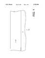
- FIG. 1is a cross sectional side view of a wafer portion
- FIG. 2is a cross sectional side view of a wafer portion with after trench etch for shallow trench isolation
- FIG. 3is a cross sectional side view of a wafer portion with a shallow trench isolation with sidewall oxidation
- FIG. 4is a cross sectional side view of a wafer portion with a shallow trench isolation and an implant beneath the shallow trench isolation;
- FIG. 5is a cross sectional side view of a wafer portion with a finished shallow trench isolation and an implant beneath the shallow trench isolation;
- FIG. 6is a cross sectional side view of a wafer portion with devices fabricated in the n-well and p-well.
- the preferred embodiment of the present inventionovercomes the limitations of the prior art and provides a device and method to increase the latch-up immunity of CMOS devices by decreasing carrier mobility between n-channel and p-channel devices. This is accomplished by forming an implant between the devices.
- the implantis formed beneath a shallow trench isolation (STI) between the n-channel and p-channel devices.
- STIshallow trench isolation
- the implantcan be formed without requiring additional high energy implants or additional mask levels.
- FIG. 1is a cross-sectional schematic view of wafer portion 100 on which a CMOS device will be fabricated.
- the wafer portion 100comprises a p+ substrate with a p- epitaxial layer at the top portion.
- CMOS deviceCMOS device
- shallow trench isolation (STI) 102is used to separate n-channel from p-channel devices.
- the STIcan be formed with any suitable processing method, such as reactive ion etching (RIE).
- RIEreactive ion etching
- a masking layer 104is deposited across the wafer 100.
- the masking layercan comprise any suitable material, for example, a layer of silicon dioxide (SiO 2 ) under a layer of silicon nitride (SiN) is a commonly used material that may be patterned to form an etch mask.
- the masking layer 104is then patterned using conventional photolithography techniques.
- the STI 102is then formed by etching away portions of the wafer no longer covered by masking layer 104.
- Further processing stepswill form n-channel devices and p-channel devices on the wafer portion 100. Isolation regions such as STI 102 are formed between these various devices (i.e., between two n-channel devices, between two p-channel devices and between an n-channel and a p-channel device. In all these cases the STI 102 serves to isolate the devices from each other.
- the preferred embodimentresults in less mobility for carriers beneath the STI 102 and thus allows the STI 102 to be more shallow than prior art STI's and still maintain effective isolation between devices.
- the preferred embodimentimproves the scalibility of STI without decreasing the latch-up immunity.
- the next stepis to grow sidewall oxidation 110 (suitably SiO 2 ) in the STI trench.
- the sidewall oxidation 110serves to reduce stress incurred by the STI etch and to remove surface contaminants.
- the latch-up immunityis increased by reducing the mobility of carriers that travel under the STI 102.
- an implant or implantsare used that improves the latch-up holding voltage. These implants can be made without additional masks.
- a speciesis implanted forming implant 106 underneath STI 102.
- the implantationcan be done with any suitable procedure, such as traditional ion implantation techniques.
- the masking layer 104blocks the implants from entering the other portions of wafer 100.
- the implantis self aligned, and does not require additional masks or process steps.
- the implantscan comprise any suitable material that would sufficiently degrade conductor mobility beneath STI 102.
- elements for implantsare selected to minimize n-well or p-well counterdoping, and as such the preferred implant would result in minimal doping change for the adjacent n-wells or p-wells.
- the preferred implantshould be selected to have low diffusitivity, thus reducing the probability of the implants diffusing into neighboring devices.
- the elementspreferably comprise large, heavy elements. Large elements result in an increased probability of scattering, and hence significantly decrease the mobility of the conductors beneath the STI. When latch-up occurs, the current flows almost entirely beneath the STI 102, thus reductions in the mobility beneath the STI 102 will increase the latch-up holding voltage.
- the preferred implantscan be electrically neutral species, such as argon (Ar), germanium (Ge), oxygen (0), nitrogen (N), and would thus decrease the mobility of carriers with a very low change to the dopant profile of the substrate.
- the implantscan be p-type and n-type materials used in combination to reduce the mobility while resulting a low net dopant profile changes.
- speciessuch as indium (In) in combination with antimony (Sb) and phosphorus (P) in combination with boron (B) can be used.
- the implantsare preferably either a counter doping combination of n-type and p-type materials to minimize effects to neighboring wells, or an electrically inactive species.
- the implantsare preferably implanted at relatively low energies to keep the implants directly under the STI 102.
- the implant 106is formed before the formation of the sidewall oxidation 110.
- the fabrication of the wafercontinues.
- the STI trenchis then filled and the wafer 100 is then planaraized with a chemical mechanical polish (CMP). This removes the remaining masking layer 104 and excess sidewall oxidation, resulting in the finished shallow trench isolation.
- CMPchemical mechanical polish
- a n-channel deviceincluding a gate 602, gate oxide 604 and diffusions 606 and 608 are formed in the p-well 610.
- a p-channel deviceincluding a gate 612, gate oxide 614 and diffusions 616 and 618 are formed in the n-well 620.
- the implant 106serves to increase the latch-up holding voltage by reducing carrier mobility between the devices. This increases the latch-up immunity of the CMOS devices.
Landscapes
- Engineering & Computer Science (AREA)
- Physics & Mathematics (AREA)
- Condensed Matter Physics & Semiconductors (AREA)
- General Physics & Mathematics (AREA)
- Manufacturing & Machinery (AREA)
- Computer Hardware Design (AREA)
- Microelectronics & Electronic Packaging (AREA)
- Power Engineering (AREA)
- Metal-Oxide And Bipolar Metal-Oxide Semiconductor Integrated Circuits (AREA)
- Element Separation (AREA)
Abstract
Description
Claims (8)
Priority Applications (7)
| Application Number | Priority Date | Filing Date | Title |
|---|---|---|---|
| US08/819,615US5770504A (en) | 1997-03-17 | 1997-03-17 | Method for increasing latch-up immunity in CMOS devices |
| TW086119222ATW353796B (en) | 1997-03-17 | 1997-12-18 | Method and device to increase latch-up immunity in CMOS devices |
| KR1019980001521AKR100288669B1 (en) | 1997-03-17 | 1998-01-20 | Method and device to increase latch-up immunity in cmos devices |
| MYPI98000730AMY120978A (en) | 1997-03-17 | 1998-02-20 | Method and device to increase latch- up immunity in cmos device |
| JP10039909AJP2938422B2 (en) | 1997-03-17 | 1998-02-23 | Method and apparatus for increasing latch-up immunity in CMOS devices |
| SG1998000433ASG60207A1 (en) | 1997-03-17 | 1998-02-26 | Method and device to increase latch-up immunity in cmos devices |
| US09/044,356US20010011758A1 (en) | 1997-03-17 | 1998-03-19 | Method and device to increase latch-up immunity in cmos device |
Applications Claiming Priority (1)
| Application Number | Priority Date | Filing Date | Title |
|---|---|---|---|
| US08/819,615US5770504A (en) | 1997-03-17 | 1997-03-17 | Method for increasing latch-up immunity in CMOS devices |
Related Child Applications (1)
| Application Number | Title | Priority Date | Filing Date |
|---|---|---|---|
| US09/044,356DivisionUS20010011758A1 (en) | 1997-03-17 | 1998-03-19 | Method and device to increase latch-up immunity in cmos device |
Publications (1)
| Publication Number | Publication Date |
|---|---|
| US5770504Atrue US5770504A (en) | 1998-06-23 |
Family
ID=25228617
Family Applications (2)
| Application Number | Title | Priority Date | Filing Date |
|---|---|---|---|
| US08/819,615Expired - LifetimeUS5770504A (en) | 1997-03-17 | 1997-03-17 | Method for increasing latch-up immunity in CMOS devices |
| US09/044,356AbandonedUS20010011758A1 (en) | 1997-03-17 | 1998-03-19 | Method and device to increase latch-up immunity in cmos device |
Family Applications After (1)
| Application Number | Title | Priority Date | Filing Date |
|---|---|---|---|
| US09/044,356AbandonedUS20010011758A1 (en) | 1997-03-17 | 1998-03-19 | Method and device to increase latch-up immunity in cmos device |
Country Status (6)
| Country | Link |
|---|---|
| US (2) | US5770504A (en) |
| JP (1) | JP2938422B2 (en) |
| KR (1) | KR100288669B1 (en) |
| MY (1) | MY120978A (en) |
| SG (1) | SG60207A1 (en) |
| TW (1) | TW353796B (en) |
Cited By (40)
| Publication number | Priority date | Publication date | Assignee | Title |
|---|---|---|---|---|
| US5970362A (en)* | 1997-12-18 | 1999-10-19 | Advanced Micro Devices, Inc. | Simplified shallow trench isolation formation with no polish stop |
| US6133123A (en)* | 1997-08-21 | 2000-10-17 | Micron Technology, Inc. | Fabrication of semiconductor gettering structures by ion implantation |
| US6144086A (en)* | 1999-04-30 | 2000-11-07 | International Business Machines Corporation | Structure for improved latch-up using dual depth STI with impurity implant |
| US6177333B1 (en)* | 1999-01-14 | 2001-01-23 | Micron Technology, Inc. | Method for making a trench isolation for semiconductor devices |
| US6218704B1 (en)* | 1997-05-07 | 2001-04-17 | International Business Machines Corporation | ESD protection structure and method |
| US6232165B1 (en)* | 1998-12-09 | 2001-05-15 | Winbond Electronics Corporation | Buried guard rings and method for forming the same |
| US6235610B1 (en)* | 1998-01-13 | 2001-05-22 | Stmicroelectronics S.R.L. | Process for selectively implanting dopants into the bottom of a deep trench |
| US6245639B1 (en)* | 1999-02-08 | 2001-06-12 | Taiwan Semiconductor Manufacturing Company | Method to reduce a reverse narrow channel effect for MOSFET devices |
| KR20010066388A (en)* | 1999-12-31 | 2001-07-11 | 박종섭 | Method for forming semiconductor device with trench type isolation layer |
| US6262453B1 (en)* | 1998-04-24 | 2001-07-17 | Magepower Semiconductor Corp. | Double gate-oxide for reducing gate-drain capacitance in trenched DMOS with high-dopant concentration buried-region under trenched gate |
| US6423615B1 (en) | 1999-09-22 | 2002-07-23 | Intel Corporation | Silicon wafers for CMOS and other integrated circuits |
| US6465283B1 (en)* | 2000-02-01 | 2002-10-15 | Industrial Technology Research Institute | Structure and fabrication method using latch-up implantation for improving latch-up immunity in CMOS fabrication process |
| US6504219B1 (en)* | 1999-12-22 | 2003-01-07 | Lsi Logic Corporation | Indium field implant for punchthrough protection in semiconductor devices |
| US6514833B1 (en)* | 1999-09-24 | 2003-02-04 | Advanced Micro Devices, Inc. | Method of inhibiting lateral diffusion between adjacent wells by introducing carbon or fluorine ions into bottom of STI groove |
| US20030038337A1 (en)* | 1998-12-28 | 2003-02-27 | Kenji Kanamitsu | Semiconductor integrated circuit device and a method of manufacturing the same |
| US6537888B2 (en)* | 2000-07-26 | 2003-03-25 | Samsung Electronics Co., Ltd. | Method for fabricating a semiconductor device reducing junction leakage current and narrow width effect |
| US20030162400A1 (en)* | 2002-02-22 | 2003-08-28 | International Business Machines Corporation | Deep trench isolation of embedded DRAM for improved latch-up immunity |
| US6686252B2 (en)* | 2001-03-10 | 2004-02-03 | International Business Machines Corporation | Method and structure to reduce CMOS inter-well leakage |
| US20040132263A1 (en)* | 2002-07-24 | 2004-07-08 | Jae-Kyu Lee | Method for forming shallow well of semiconductor device using low-energy ion implantation |
| KR100449318B1 (en)* | 2001-12-20 | 2004-09-18 | 동부전자 주식회사 | Method for forming isolation layer in semiconductor device |
| US20040219769A1 (en)* | 2001-11-16 | 2004-11-04 | Voldman Steven H. | Method and structure for improving latch-up immunity using non-dopant implants |
| US20040251511A1 (en)* | 2002-05-07 | 2004-12-16 | Agere Systems Inc. | Semiconductor device including an isolation trench having a dopant barrier layer formed on a sidewall thereof and a method of manufacture therefor |
| US20050095804A1 (en)* | 2003-09-19 | 2005-05-05 | Atmel Germany Gmbh | Method of fabricating semiconductor components through implantation and diffusion in a semiconductor substrate |
| US7012316B1 (en) | 2004-09-17 | 2006-03-14 | International Business Machines Corporation | Isolation structures in semiconductor integrated circuits (IC) |
| US20060076582A1 (en)* | 2003-03-03 | 2006-04-13 | Matsushita Electric Industrial Co., Ltd. | Solid-state imaging device, method for manufacturing the same and interline transfer CCD image sensor |
| US20070122963A1 (en)* | 2005-11-28 | 2007-05-31 | Via Technologies, Inc. Of R.O.C. | Latch-up prevention in semiconductor circuits |
| US20070161207A1 (en)* | 2005-12-28 | 2007-07-12 | Hyuk Park | Method for Manufacturing Semiconductor Device |
| US20070170517A1 (en)* | 2006-01-26 | 2007-07-26 | International Business Machines Corporation | CMOS devices adapted to reduce latchup and methods of manufacturing the same |
| US7391200B1 (en) | 2007-02-02 | 2008-06-24 | Netlogic Microsystems, Inc. | P-channel power chip |
| US20080171413A1 (en)* | 2007-01-17 | 2008-07-17 | International Business Machines Corporation | Method of Reducing Detrimental STI-Induced Stress in MOSFET Channels |
| US20080211064A1 (en)* | 2007-03-01 | 2008-09-04 | Orner Bradley A | Deep trench based far subcollector reachthrough |
| KR100948296B1 (en) | 2007-11-30 | 2010-03-17 | 주식회사 동부하이텍 | Manufacturing Method of Semiconductor Device |
| US7808223B1 (en) | 2007-05-08 | 2010-10-05 | Netlogic Microsystems, Inc. | Transistor with spatially integrated schottky diode |
| US20110284985A1 (en)* | 2010-05-20 | 2011-11-24 | Globalfoundries Inc. | Shallow trench isolation extension |
| US8274265B1 (en) | 2007-02-28 | 2012-09-25 | Netlogic Microsystems, Inc. | Multi-phase power system with redundancy |
| CN103137618A (en)* | 2011-12-01 | 2013-06-05 | 台湾积体电路制造股份有限公司 | Localized carrier lifetime reduction |
| KR20140108952A (en)* | 2013-03-04 | 2014-09-15 | 삼성전자주식회사 | Method of manufacturing a semiconductor device |
| US9196729B2 (en) | 2013-07-17 | 2015-11-24 | Samsung Electronics Co., Ltd. | Semiconductor device having buried channel array and method of manufacturing the same |
| US20160300906A1 (en)* | 2015-04-07 | 2016-10-13 | Taiwan Semiconductor Manufacturing Company, Ltd. | Semiconductor device having barrier layer to prevent impurity diffusion |
| US11164746B2 (en)* | 2018-06-26 | 2021-11-02 | Taiwan Semiconductor Manufacturing Co., Ltd. | Method of manufacturing semiconductor devices and a semiconductor device |
Families Citing this family (2)
| Publication number | Priority date | Publication date | Assignee | Title |
|---|---|---|---|---|
| KR20030096703A (en)* | 2002-06-17 | 2003-12-31 | 주식회사 하이닉스반도체 | method for fabricating semicinductor device |
| US7750429B2 (en)* | 2007-05-15 | 2010-07-06 | International Business Machines Corporation | Self-aligned and extended inter-well isolation structure |
Citations (17)
| Publication number | Priority date | Publication date | Assignee | Title |
|---|---|---|---|---|
| US4027380A (en)* | 1974-06-03 | 1977-06-07 | Fairchild Camera And Instrument Corporation | Complementary insulated gate field effect transistor structure and process for fabricating the structure |
| US4470852A (en)* | 1982-09-03 | 1984-09-11 | Ncr Corporation | Method of making CMOS device and contacts therein by enhanced oxidation of selectively implanted regions |
| US4477310A (en)* | 1983-08-12 | 1984-10-16 | Tektronix, Inc. | Process for manufacturing MOS integrated circuit with improved method of forming refractory metal silicide areas |
| US4578128A (en)* | 1984-12-03 | 1986-03-25 | Ncr Corporation | Process for forming retrograde dopant distributions utilizing simultaneous outdiffusion of dopants |
| US4599789A (en)* | 1984-06-15 | 1986-07-15 | Harris Corporation | Process of making twin well VLSI CMOS |
| US4646123A (en)* | 1983-10-11 | 1987-02-24 | At&T Bell Laboratories | Latchup-preventing CMOS device |
| US4647957A (en)* | 1983-10-11 | 1987-03-03 | At&T Bell Laboratories | Latchup-preventing CMOS device |
| US4653177A (en)* | 1985-07-25 | 1987-03-31 | At&T Bell Laboratories | Method of making and selectively doping isolation trenches utilized in CMOS devices |
| US4656730A (en)* | 1984-11-23 | 1987-04-14 | American Telephone And Telegraph Company, At&T Bell Laboratories | Method for fabricating CMOS devices |
| US4683488A (en)* | 1984-03-29 | 1987-07-28 | Hughes Aircraft Company | Latch-up resistant CMOS structure for VLSI including retrograded wells |
| US4729006A (en)* | 1986-03-17 | 1988-03-01 | International Business Machines Corporation | Sidewall spacers for CMOS circuit stress relief/isolation and method for making |
| US4766090A (en)* | 1986-04-21 | 1988-08-23 | American Telephone And Telegraph Company, At&T Bell Laboratories | Methods for fabricating latchup-preventing CMOS device |
| US4947227A (en)* | 1985-09-16 | 1990-08-07 | Texas Instruments, Incorporated | Latch-up resistant CMOS structure |
| US4963502A (en)* | 1988-08-25 | 1990-10-16 | Texas Instruments, Incorporated | Method of making oxide-isolated source/drain transistor |
| US5179038A (en)* | 1989-12-22 | 1993-01-12 | North American Philips Corp., Signetics Division | High density trench isolation for MOS circuits |
| US5420061A (en)* | 1993-08-13 | 1995-05-30 | Micron Semiconductor, Inc. | Method for improving latchup immunity in a dual-polysilicon gate process |
| US5536675A (en)* | 1993-12-30 | 1996-07-16 | Intel Corporation | Isolation structure formation for semiconductor circuit fabrication |
- 1997
- 1997-03-17USUS08/819,615patent/US5770504A/ennot_activeExpired - Lifetime
- 1997-12-18TWTW086119222Apatent/TW353796B/ennot_activeIP Right Cessation
- 1998
- 1998-01-20KRKR1019980001521Apatent/KR100288669B1/ennot_activeExpired - Fee Related
- 1998-02-20MYMYPI98000730Apatent/MY120978A/enunknown
- 1998-02-23JPJP10039909Apatent/JP2938422B2/ennot_activeExpired - Fee Related
- 1998-02-26SGSG1998000433Apatent/SG60207A1/enunknown
- 1998-03-19USUS09/044,356patent/US20010011758A1/ennot_activeAbandoned
Patent Citations (17)
| Publication number | Priority date | Publication date | Assignee | Title |
|---|---|---|---|---|
| US4027380A (en)* | 1974-06-03 | 1977-06-07 | Fairchild Camera And Instrument Corporation | Complementary insulated gate field effect transistor structure and process for fabricating the structure |
| US4470852A (en)* | 1982-09-03 | 1984-09-11 | Ncr Corporation | Method of making CMOS device and contacts therein by enhanced oxidation of selectively implanted regions |
| US4477310A (en)* | 1983-08-12 | 1984-10-16 | Tektronix, Inc. | Process for manufacturing MOS integrated circuit with improved method of forming refractory metal silicide areas |
| US4646123A (en)* | 1983-10-11 | 1987-02-24 | At&T Bell Laboratories | Latchup-preventing CMOS device |
| US4647957A (en)* | 1983-10-11 | 1987-03-03 | At&T Bell Laboratories | Latchup-preventing CMOS device |
| US4683488A (en)* | 1984-03-29 | 1987-07-28 | Hughes Aircraft Company | Latch-up resistant CMOS structure for VLSI including retrograded wells |
| US4599789A (en)* | 1984-06-15 | 1986-07-15 | Harris Corporation | Process of making twin well VLSI CMOS |
| US4656730A (en)* | 1984-11-23 | 1987-04-14 | American Telephone And Telegraph Company, At&T Bell Laboratories | Method for fabricating CMOS devices |
| US4578128A (en)* | 1984-12-03 | 1986-03-25 | Ncr Corporation | Process for forming retrograde dopant distributions utilizing simultaneous outdiffusion of dopants |
| US4653177A (en)* | 1985-07-25 | 1987-03-31 | At&T Bell Laboratories | Method of making and selectively doping isolation trenches utilized in CMOS devices |
| US4947227A (en)* | 1985-09-16 | 1990-08-07 | Texas Instruments, Incorporated | Latch-up resistant CMOS structure |
| US4729006A (en)* | 1986-03-17 | 1988-03-01 | International Business Machines Corporation | Sidewall spacers for CMOS circuit stress relief/isolation and method for making |
| US4766090A (en)* | 1986-04-21 | 1988-08-23 | American Telephone And Telegraph Company, At&T Bell Laboratories | Methods for fabricating latchup-preventing CMOS device |
| US4963502A (en)* | 1988-08-25 | 1990-10-16 | Texas Instruments, Incorporated | Method of making oxide-isolated source/drain transistor |
| US5179038A (en)* | 1989-12-22 | 1993-01-12 | North American Philips Corp., Signetics Division | High density trench isolation for MOS circuits |
| US5420061A (en)* | 1993-08-13 | 1995-05-30 | Micron Semiconductor, Inc. | Method for improving latchup immunity in a dual-polysilicon gate process |
| US5536675A (en)* | 1993-12-30 | 1996-07-16 | Intel Corporation | Isolation structure formation for semiconductor circuit fabrication |
Cited By (83)
| Publication number | Priority date | Publication date | Assignee | Title |
|---|---|---|---|---|
| US6218704B1 (en)* | 1997-05-07 | 2001-04-17 | International Business Machines Corporation | ESD protection structure and method |
| US6465873B1 (en)* | 1997-08-21 | 2002-10-15 | Micron Technology, Inc. | Semiconductor gettering structures |
| US6133123A (en)* | 1997-08-21 | 2000-10-17 | Micron Technology, Inc. | Fabrication of semiconductor gettering structures by ion implantation |
| US6509248B1 (en)* | 1997-08-21 | 2003-01-21 | Micron Technology, Inc. | Fabrication of semiconductor gettering structures by ion implantation |
| US6479875B1 (en) | 1997-08-21 | 2002-11-12 | Micron Technology, Inc. | Fabrication of semiconductor gettering structures by ion implantation |
| US5970362A (en)* | 1997-12-18 | 1999-10-19 | Advanced Micro Devices, Inc. | Simplified shallow trench isolation formation with no polish stop |
| US6235610B1 (en)* | 1998-01-13 | 2001-05-22 | Stmicroelectronics S.R.L. | Process for selectively implanting dopants into the bottom of a deep trench |
| US6262453B1 (en)* | 1998-04-24 | 2001-07-17 | Magepower Semiconductor Corp. | Double gate-oxide for reducing gate-drain capacitance in trenched DMOS with high-dopant concentration buried-region under trenched gate |
| US6232165B1 (en)* | 1998-12-09 | 2001-05-15 | Winbond Electronics Corporation | Buried guard rings and method for forming the same |
| US6476451B2 (en)* | 1998-12-09 | 2002-11-05 | Winbond Electronics Corporation | Buried guard rings for CMOS device |
| US6544839B1 (en)* | 1998-12-28 | 2003-04-08 | Hitachi, Ltd. | Semiconductor integrated circuit device and a method of manufacturing the same |
| US20050014340A1 (en)* | 1998-12-28 | 2005-01-20 | Kenji Kanamitsu | Method of manufacturing a semiconductor integrated circuit device having a trench |
| US6967141B2 (en) | 1998-12-28 | 2005-11-22 | Renesas Technology Corp. | Method of manufacturing a semiconductor integrated circuit device having a trench |
| US20050260820A1 (en)* | 1998-12-28 | 2005-11-24 | Kenji Kanamitsu | Method of manufacturing a semiconductor integrated circuit device having a trench |
| US7524729B2 (en) | 1998-12-28 | 2009-04-28 | Renesas Technology Corp. | Method of manufacturing a semiconductor integrated circuit device having a trench |
| US20030038337A1 (en)* | 1998-12-28 | 2003-02-27 | Kenji Kanamitsu | Semiconductor integrated circuit device and a method of manufacturing the same |
| US20040262641A1 (en)* | 1999-01-14 | 2004-12-30 | Rhodes Howard E. | Trench isolation for semiconductor devices |
| US20010013631A1 (en)* | 1999-01-14 | 2001-08-16 | Howard E. Rhodes | Trench isolation for semiconductor devices |
| US6177333B1 (en)* | 1999-01-14 | 2001-01-23 | Micron Technology, Inc. | Method for making a trench isolation for semiconductor devices |
| US7071531B2 (en) | 1999-01-14 | 2006-07-04 | Micron Technology, Inc. | Trench isolation for semiconductor devices |
| US20060244015A1 (en)* | 1999-01-14 | 2006-11-02 | Rhodes Howard E | Trench isolation for semiconductor devices |
| US6245639B1 (en)* | 1999-02-08 | 2001-06-12 | Taiwan Semiconductor Manufacturing Company | Method to reduce a reverse narrow channel effect for MOSFET devices |
| US6144086A (en)* | 1999-04-30 | 2000-11-07 | International Business Machines Corporation | Structure for improved latch-up using dual depth STI with impurity implant |
| US6667522B2 (en) | 1999-09-22 | 2003-12-23 | Intel Corporation | Silicon wafers for CMOS and other integrated circuits |
| US6423615B1 (en) | 1999-09-22 | 2002-07-23 | Intel Corporation | Silicon wafers for CMOS and other integrated circuits |
| US6514833B1 (en)* | 1999-09-24 | 2003-02-04 | Advanced Micro Devices, Inc. | Method of inhibiting lateral diffusion between adjacent wells by introducing carbon or fluorine ions into bottom of STI groove |
| US6504219B1 (en)* | 1999-12-22 | 2003-01-07 | Lsi Logic Corporation | Indium field implant for punchthrough protection in semiconductor devices |
| KR20010066388A (en)* | 1999-12-31 | 2001-07-11 | 박종섭 | Method for forming semiconductor device with trench type isolation layer |
| US6465283B1 (en)* | 2000-02-01 | 2002-10-15 | Industrial Technology Research Institute | Structure and fabrication method using latch-up implantation for improving latch-up immunity in CMOS fabrication process |
| US6740954B2 (en)* | 2000-07-26 | 2004-05-25 | Samsung Electronics Co, Ltd. | Semiconductor device reducing junction leakage current and narrow width effect |
| US6537888B2 (en)* | 2000-07-26 | 2003-03-25 | Samsung Electronics Co., Ltd. | Method for fabricating a semiconductor device reducing junction leakage current and narrow width effect |
| US6946710B2 (en) | 2001-03-10 | 2005-09-20 | International Business Machines Corporation | Method and structure to reduce CMOS inter-well leakage |
| US20040166620A1 (en)* | 2001-03-10 | 2004-08-26 | Logan Lyndon R. | Method and structure to reduce CMOS inter-well leakage |
| US6686252B2 (en)* | 2001-03-10 | 2004-02-03 | International Business Machines Corporation | Method and structure to reduce CMOS inter-well leakage |
| US7041581B2 (en) | 2001-11-16 | 2006-05-09 | International Business Machines Corporation | Method and structure for improving latch-up immunity using non-dopant implants |
| US20040219769A1 (en)* | 2001-11-16 | 2004-11-04 | Voldman Steven H. | Method and structure for improving latch-up immunity using non-dopant implants |
| KR100449318B1 (en)* | 2001-12-20 | 2004-09-18 | 동부전자 주식회사 | Method for forming isolation layer in semiconductor device |
| US7138319B2 (en) | 2002-02-22 | 2006-11-21 | International Business Machines Corporation | Deep trench isolation of embedded DRAM for improved latch-up immunity |
| US6885080B2 (en) | 2002-02-22 | 2005-04-26 | International Business Machines Corporation | Deep trench isolation of embedded DRAM for improved latch-up immunity |
| US20050106836A1 (en)* | 2002-02-22 | 2005-05-19 | Tze-Chiang Chen | Deep trench isolation of embedded dram for improved latch-up immunity |
| US20030162400A1 (en)* | 2002-02-22 | 2003-08-28 | International Business Machines Corporation | Deep trench isolation of embedded DRAM for improved latch-up immunity |
| US20040251511A1 (en)* | 2002-05-07 | 2004-12-16 | Agere Systems Inc. | Semiconductor device including an isolation trench having a dopant barrier layer formed on a sidewall thereof and a method of manufacture therefor |
| CN100359665C (en)* | 2002-07-24 | 2008-01-02 | 三星电子株式会社 | Method of forming shallow wells of semiconductor devices using low energy ion implantation |
| US20040132263A1 (en)* | 2002-07-24 | 2004-07-08 | Jae-Kyu Lee | Method for forming shallow well of semiconductor device using low-energy ion implantation |
| US6844239B2 (en)* | 2002-07-24 | 2005-01-18 | Samsung Electronics Co., Ltd. | Method for forming shallow well of semiconductor device using low-energy ion implantation |
| US20060076582A1 (en)* | 2003-03-03 | 2006-04-13 | Matsushita Electric Industrial Co., Ltd. | Solid-state imaging device, method for manufacturing the same and interline transfer CCD image sensor |
| EP1455389A3 (en)* | 2003-03-03 | 2009-04-01 | Panasonic Corporation | Solid-state imaging device, method for manufacturing the same and interline transfer CCD image sensor |
| US7358105B2 (en)* | 2003-03-03 | 2008-04-15 | Matsushita Electric Industrial Co., Ltd. | Solid-state imaging device, method for manufacturing the same and interline transfer CCD image sensor |
| US20050095804A1 (en)* | 2003-09-19 | 2005-05-05 | Atmel Germany Gmbh | Method of fabricating semiconductor components through implantation and diffusion in a semiconductor substrate |
| US7144796B2 (en)* | 2003-09-19 | 2006-12-05 | Atmel Germany Gmbh | Method of fabricating semiconductor components through implantation and diffusion in a semiconductor substrate |
| CN100392816C (en)* | 2003-09-19 | 2008-06-04 | Atmel德国有限公司 | Method for manufacturing a semiconductor element in a semiconductor substrate |
| US7012316B1 (en) | 2004-09-17 | 2006-03-14 | International Business Machines Corporation | Isolation structures in semiconductor integrated circuits (IC) |
| US20060060935A1 (en)* | 2004-09-17 | 2006-03-23 | International Business Machines Corporation | Isolation structures in semiconductor integrated circuits (ic) |
| US20070122963A1 (en)* | 2005-11-28 | 2007-05-31 | Via Technologies, Inc. Of R.O.C. | Latch-up prevention in semiconductor circuits |
| US20070161207A1 (en)* | 2005-12-28 | 2007-07-12 | Hyuk Park | Method for Manufacturing Semiconductor Device |
| US20070170517A1 (en)* | 2006-01-26 | 2007-07-26 | International Business Machines Corporation | CMOS devices adapted to reduce latchup and methods of manufacturing the same |
| US7618857B2 (en)* | 2007-01-17 | 2009-11-17 | International Business Machines Corporation | Method of reducing detrimental STI-induced stress in MOSFET channels |
| US20080171413A1 (en)* | 2007-01-17 | 2008-07-17 | International Business Machines Corporation | Method of Reducing Detrimental STI-Induced Stress in MOSFET Channels |
| US7391200B1 (en) | 2007-02-02 | 2008-06-24 | Netlogic Microsystems, Inc. | P-channel power chip |
| US8274265B1 (en) | 2007-02-28 | 2012-09-25 | Netlogic Microsystems, Inc. | Multi-phase power system with redundancy |
| US8836306B2 (en) | 2007-02-28 | 2014-09-16 | Netlogic Microsystems, Inc. | Multi-phase power system with redundancy |
| US8901909B2 (en) | 2007-02-28 | 2014-12-02 | Netlogic Microsystems, Inc. | Multi-phase power system with redundancy |
| US8105924B2 (en) | 2007-03-01 | 2012-01-31 | International Business Machines Corporation | Deep trench based far subcollector reachthrough |
| US20100117189A1 (en)* | 2007-03-01 | 2010-05-13 | International Business Machines Corporation | Deep trench based far subcollector reachthrough |
| US20080211064A1 (en)* | 2007-03-01 | 2008-09-04 | Orner Bradley A | Deep trench based far subcollector reachthrough |
| US7691734B2 (en)* | 2007-03-01 | 2010-04-06 | International Business Machines Corporation | Deep trench based far subcollector reachthrough |
| US7808223B1 (en) | 2007-05-08 | 2010-10-05 | Netlogic Microsystems, Inc. | Transistor with spatially integrated schottky diode |
| KR100948296B1 (en) | 2007-11-30 | 2010-03-17 | 주식회사 동부하이텍 | Manufacturing Method of Semiconductor Device |
| US8956948B2 (en)* | 2010-05-20 | 2015-02-17 | Globalfoundries Inc. | Shallow trench isolation extension |
| US20110284985A1 (en)* | 2010-05-20 | 2011-11-24 | Globalfoundries Inc. | Shallow trench isolation extension |
| US20130140667A1 (en)* | 2011-12-01 | 2013-06-06 | Taiwan Semiconductor Manufacturing Company, Ltd. | Localized carrier lifetime reduction |
| CN103137618A (en)* | 2011-12-01 | 2013-06-05 | 台湾积体电路制造股份有限公司 | Localized carrier lifetime reduction |
| US9698044B2 (en)* | 2011-12-01 | 2017-07-04 | Taiwan Semiconductor Manufacturing Company, Ltd. | Localized carrier lifetime reduction |
| US10381259B2 (en) | 2011-12-01 | 2019-08-13 | Taiwan Semiconductor Manufacturing Company, Ltd. | Semiconductor device with localized carrier lifetime reduction and fabrication method thereof |
| KR20140108952A (en)* | 2013-03-04 | 2014-09-15 | 삼성전자주식회사 | Method of manufacturing a semiconductor device |
| US9490160B2 (en) | 2013-03-04 | 2016-11-08 | Samsung Electronics Co., Ltd. | Method of manufacturing semiconductor device |
| US9196729B2 (en) | 2013-07-17 | 2015-11-24 | Samsung Electronics Co., Ltd. | Semiconductor device having buried channel array and method of manufacturing the same |
| US9728598B2 (en)* | 2015-04-07 | 2017-08-08 | Taiwan Semiconductor Manufacturing Co., Ltd. | Semiconductor device having barrier layer to prevent impurity diffusion |
| US20170317164A1 (en)* | 2015-04-07 | 2017-11-02 | Taiwan Semiconductor Manufacturing Co., Ltd. | Semiconductor device having barrier layer to prevent impurity diffusion |
| US10096672B2 (en)* | 2015-04-07 | 2018-10-09 | Taiwan Semiconductor Manufacturing Co., Ltd. | Semiconductor device having barrier layer to prevent impurity diffusion |
| US20160300906A1 (en)* | 2015-04-07 | 2016-10-13 | Taiwan Semiconductor Manufacturing Company, Ltd. | Semiconductor device having barrier layer to prevent impurity diffusion |
| US11164746B2 (en)* | 2018-06-26 | 2021-11-02 | Taiwan Semiconductor Manufacturing Co., Ltd. | Method of manufacturing semiconductor devices and a semiconductor device |
| US11908864B2 (en) | 2018-06-26 | 2024-02-20 | Taiwan Semiconductor Manufacturing Company, Ltd. | Method of manufacturing semiconductor devices and a semiconductor device |
Also Published As
| Publication number | Publication date |
|---|---|
| MY120978A (en) | 2005-12-30 |
| US20010011758A1 (en) | 2001-08-09 |
| JPH10261766A (en) | 1998-09-29 |
| JP2938422B2 (en) | 1999-08-23 |
| KR100288669B1 (en) | 2001-06-01 |
| TW353796B (en) | 1999-03-01 |
| KR19980079630A (en) | 1998-11-25 |
| SG60207A1 (en) | 1999-02-22 |
Similar Documents
| Publication | Publication Date | Title |
|---|---|---|
| US5770504A (en) | Method for increasing latch-up immunity in CMOS devices | |
| EP0661751B1 (en) | Method of making a CMOS device with high and low voltage transistors | |
| US6445044B2 (en) | Apparatus improving latchup immunity in a dual-polysilicon gate | |
| US6228726B1 (en) | Method to suppress CMOS device latchup and improve interwell isolation | |
| US4435896A (en) | Method for fabricating complementary field effect transistor devices | |
| US5416351A (en) | Electrostatic discharge protection | |
| KR100243715B1 (en) | CMOS structure with FET in isolated well with depletion unit and method | |
| US4835115A (en) | Method for forming oxide-capped trench isolation | |
| US20070158779A1 (en) | Methods and semiconductor structures for latch-up suppression using a buried damage layer | |
| US20060220109A1 (en) | Selectively doped trench device isolation | |
| JPH0332224B2 (en) | ||
| JP3364903B2 (en) | Deep divot mask for improving performance and reliability of buried channel PFET | |
| US4707456A (en) | Method of making a planar structure containing MOS and bipolar transistors | |
| US6514833B1 (en) | Method of inhibiting lateral diffusion between adjacent wells by introducing carbon or fluorine ions into bottom of STI groove | |
| KR20020094955A (en) | Semiconductor device with sti sidewall implant | |
| US7095087B2 (en) | Semiconductor device and fabrication method thereof | |
| US6855618B2 (en) | Radiation hardened semiconductor device | |
| JP2534991B2 (en) | Manufacturing method of CMOS structure | |
| US6083795A (en) | Large angle channel threshold implant for improving reverse narrow width effect | |
| US6011283A (en) | Pillar emitter for BiCMOS devices | |
| US6933203B2 (en) | Methods for improving well to well isolation | |
| US6790722B1 (en) | Logic SOI structure, process and application for vertical bipolar transistor | |
| US20030062572A1 (en) | Transistor with bottomwall/sidewall junction capacitance reduction region and method | |
| US6890832B1 (en) | Radiation hardening method for shallow trench isolation in CMOS | |
| US5049519A (en) | Latch-up resistant CMOS process |
Legal Events
| Date | Code | Title | Description |
|---|---|---|---|
| AS | Assignment | Owner name:INTERNATIONAL BUSINESS MACHINES CORPORATION, NEW Y Free format text:ASSIGNMENT OF ASSIGNORS INTEREST;ASSIGNORS:BROWN, JEFFREY S.;GAUTHIER, JR. ROBERT J;TIAN, XIAOWEI;REEL/FRAME:008590/0164 Effective date:19970312 | |
| STCF | Information on status: patent grant | Free format text:PATENTED CASE | |
| CC | Certificate of correction | ||
| FEPP | Fee payment procedure | Free format text:PAYOR NUMBER ASSIGNED (ORIGINAL EVENT CODE: ASPN); ENTITY STATUS OF PATENT OWNER: LARGE ENTITY | |
| FPAY | Fee payment | Year of fee payment:4 | |
| FPAY | Fee payment | Year of fee payment:8 | |
| FPAY | Fee payment | Year of fee payment:12 | |
| AS | Assignment | Owner name:GLOBALFOUNDRIES U.S. 2 LLC, NEW YORK Free format text:ASSIGNMENT OF ASSIGNORS INTEREST;ASSIGNOR:INTERNATIONAL BUSINESS MACHINES CORPORATION;REEL/FRAME:036550/0001 Effective date:20150629 | |
| AS | Assignment | Owner name:GLOBALFOUNDRIES INC., CAYMAN ISLANDS Free format text:ASSIGNMENT OF ASSIGNORS INTEREST;ASSIGNORS:GLOBALFOUNDRIES U.S. 2 LLC;GLOBALFOUNDRIES U.S. INC.;REEL/FRAME:036779/0001 Effective date:20150910 | |
| AS | Assignment | Owner name:GLOBALFOUNDRIES U.S. INC., NEW YORK Free format text:RELEASE BY SECURED PARTY;ASSIGNOR:WILMINGTON TRUST, NATIONAL ASSOCIATION;REEL/FRAME:056987/0001 Effective date:20201117 |