US5770465A - Trench-filling etch-masking microfabrication technique - Google Patents
Trench-filling etch-masking microfabrication techniqueDownload PDFInfo
- Publication number
- US5770465A US5770465AUS08/668,378US66837896AUS5770465AUS 5770465 AUS5770465 AUS 5770465AUS 66837896 AUS66837896 AUS 66837896AUS 5770465 AUS5770465 AUS 5770465A
- Authority
- US
- United States
- Prior art keywords
- trench
- substrate
- etch
- sog
- etching
- Prior art date
- Legal status (The legal status is an assumption and is not a legal conclusion. Google has not performed a legal analysis and makes no representation as to the accuracy of the status listed.)
- Expired - Lifetime
Links
- 238000000034methodMethods0.000titleclaimsabstractdescription72
- 238000011049fillingMethods0.000titleclaimsabstractdescription47
- 239000000758substrateSubstances0.000claimsabstractdescription92
- 239000000463materialSubstances0.000claimsabstractdescription27
- 238000005530etchingMethods0.000claimsabstractdescription25
- 238000004519manufacturing processMethods0.000claimsabstractdescription11
- 238000001465metallisationMethods0.000claimsdescription4
- 230000000873masking effectEffects0.000abstractdescription6
- XUIMIQQOPSSXEZ-UHFFFAOYSA-NSiliconChemical compound[Si]XUIMIQQOPSSXEZ-UHFFFAOYSA-N0.000description66
- 229910052710siliconInorganic materials0.000description63
- 239000010703siliconSubstances0.000description63
- 238000001020plasma etchingMethods0.000description50
- VYPSYNLAJGMNEJ-UHFFFAOYSA-NSilicium dioxideChemical compoundO=[Si]=OVYPSYNLAJGMNEJ-UHFFFAOYSA-N0.000description27
- 238000005229chemical vapour depositionMethods0.000description13
- 238000001459lithographyMethods0.000description13
- XPDWGBQVDMORPB-UHFFFAOYSA-NFluoroformChemical compoundFC(F)FXPDWGBQVDMORPB-UHFFFAOYSA-N0.000description10
- 239000000377silicon dioxideSubstances0.000description10
- 235000012239silicon dioxideNutrition0.000description10
- KZBUYRJDOAKODT-UHFFFAOYSA-NChlorineChemical compoundClClKZBUYRJDOAKODT-UHFFFAOYSA-N0.000description9
- 229910052751metalInorganic materials0.000description9
- 239000002184metalSubstances0.000description9
- 235000012431wafersNutrition0.000description9
- ZAMOUSCENKQFHK-UHFFFAOYSA-NChlorine atomChemical compound[Cl]ZAMOUSCENKQFHK-UHFFFAOYSA-N0.000description7
- 239000000460chlorineSubstances0.000description7
- 229910052801chlorineInorganic materials0.000description7
- 230000003287optical effectEffects0.000description7
- 229920002120photoresistant polymerPolymers0.000description7
- 229910052814silicon oxideInorganic materials0.000description7
- 238000001312dry etchingMethods0.000description6
- 230000008020evaporationEffects0.000description5
- 238000001704evaporationMethods0.000description5
- 230000007246mechanismEffects0.000description5
- KRHYYFGTRYWZRS-UHFFFAOYSA-NFluoraneChemical compoundFKRHYYFGTRYWZRS-UHFFFAOYSA-N0.000description4
- 229910001218Gallium arsenideInorganic materials0.000description4
- 230000015572biosynthetic processEffects0.000description4
- 238000000151depositionMethods0.000description4
- 230000008021depositionEffects0.000description4
- 238000005516engineering processMethods0.000description4
- 238000005755formation reactionMethods0.000description4
- 239000011521glassSubstances0.000description4
- 150000002739metalsChemical class0.000description4
- 229910052782aluminiumInorganic materials0.000description3
- XAGFODPZIPBFFR-UHFFFAOYSA-NaluminiumChemical compound[Al]XAGFODPZIPBFFR-UHFFFAOYSA-N0.000description3
- 230000008901benefitEffects0.000description3
- 239000005380borophosphosilicate glassSubstances0.000description3
- 239000003989dielectric materialSubstances0.000description3
- 238000005498polishingMethods0.000description3
- 239000007787solidSubstances0.000description3
- 229910052581Si3N4Inorganic materials0.000description2
- 238000005253claddingMethods0.000description2
- 239000013078crystalSubstances0.000description2
- 238000005429filling processMethods0.000description2
- -1reflowed oxideSubstances0.000description2
- 239000004065semiconductorSubstances0.000description2
- HQVNEWCFYHHQES-UHFFFAOYSA-Nsilicon nitrideChemical compoundN12[Si]34N5[Si]62N3[Si]51N64HQVNEWCFYHHQES-UHFFFAOYSA-N0.000description2
- OKTJSMMVPCPJKN-UHFFFAOYSA-NCarbonChemical compound[C]OKTJSMMVPCPJKN-UHFFFAOYSA-N0.000description1
- 238000000637aluminium metallisationMethods0.000description1
- 229910052799carbonInorganic materials0.000description1
- 238000000708deep reactive-ion etchingMethods0.000description1
- 238000007598dipping methodMethods0.000description1
- 238000002955isolationMethods0.000description1
- 239000007788liquidSubstances0.000description1
- 238000012986modificationMethods0.000description1
- 230000004048modificationEffects0.000description1
- 229910021421monocrystalline siliconInorganic materials0.000description1
- 238000002360preparation methodMethods0.000description1
- 230000001681protective effectEffects0.000description1
- XUIMIQQOPSSXEZ-RNFDNDRNSA-Nsilicon-32 atomChemical compound[32Si]XUIMIQQOPSSXEZ-RNFDNDRNSA-N0.000description1
- 239000002210silicon-based materialSubstances0.000description1
- 238000004528spin coatingMethods0.000description1
Images


Classifications
- B—PERFORMING OPERATIONS; TRANSPORTING
- B81—MICROSTRUCTURAL TECHNOLOGY
- B81C—PROCESSES OR APPARATUS SPECIALLY ADAPTED FOR THE MANUFACTURE OR TREATMENT OF MICROSTRUCTURAL DEVICES OR SYSTEMS
- B81C1/00—Manufacture or treatment of devices or systems in or on a substrate
- B81C1/00436—Shaping materials, i.e. techniques for structuring the substrate or the layers on the substrate
- B81C1/00555—Achieving a desired geometry, i.e. controlling etch rates, anisotropy or selectivity
- B81C1/00619—Forming high aspect ratio structures having deep steep walls
- B—PERFORMING OPERATIONS; TRANSPORTING
- B81—MICROSTRUCTURAL TECHNOLOGY
- B81C—PROCESSES OR APPARATUS SPECIALLY ADAPTED FOR THE MANUFACTURE OR TREATMENT OF MICROSTRUCTURAL DEVICES OR SYSTEMS
- B81C1/00—Manufacture or treatment of devices or systems in or on a substrate
- B81C1/00436—Shaping materials, i.e. techniques for structuring the substrate or the layers on the substrate
- B81C1/00444—Surface micromachining, i.e. structuring layers on the substrate
- B81C1/00468—Releasing structures
- B81C1/00484—Processes for releasing structures not provided for in group B81C1/00476
- B—PERFORMING OPERATIONS; TRANSPORTING
- B81—MICROSTRUCTURAL TECHNOLOGY
- B81B—MICROSTRUCTURAL DEVICES OR SYSTEMS, e.g. MICROMECHANICAL DEVICES
- B81B2203/00—Basic microelectromechanical structures
- B81B2203/01—Suspended structures, i.e. structures allowing a movement
- B81B2203/0118—Cantilevers
- B—PERFORMING OPERATIONS; TRANSPORTING
- B81—MICROSTRUCTURAL TECHNOLOGY
- B81B—MICROSTRUCTURAL DEVICES OR SYSTEMS, e.g. MICROMECHANICAL DEVICES
- B81B2203/00—Basic microelectromechanical structures
- B81B2203/03—Static structures
- B81B2203/0361—Tips, pillars
- B—PERFORMING OPERATIONS; TRANSPORTING
- B81—MICROSTRUCTURAL TECHNOLOGY
- B81C—PROCESSES OR APPARATUS SPECIALLY ADAPTED FOR THE MANUFACTURE OR TREATMENT OF MICROSTRUCTURAL DEVICES OR SYSTEMS
- B81C2201/00—Manufacture or treatment of microstructural devices or systems
- B81C2201/05—Temporary protection of devices or parts of the devices during manufacturing
- B81C2201/053—Depositing a protective layers
Definitions
- the present inventionis directed to a new microfabrication technique which uses trench filling materials as etch masks to achieve a variety of complex-shaped microstructures.
- microstructures of various topologye.g. multiple level, ultra-high aspect ratio ( ⁇ 200:1) structures.
- high aspect ratio ( ⁇ 10:1) released structures with smooth bottomsare essential in many applications.
- high quality micro-gearsrequire such a structure.
- theyhave been fabricated using LIGA process.
- LIGAsuffers from the rather complex and expensive lithographic tools involved, as well as the very thick layer deposition required which is very time and money consuming.
- the present inventionis a process which provides multiple level, ultra-high aspect ratio ( ⁇ 100:1) microstructures.
- the techniquecan be used to form ultra-high aspect ratio structures having very small gaps between each of the structures.
- multi-level, fine-line (submicron) structures of various height/widthscan now be easily fabricated on the same chip.
- the first stepis to etch deep trenches in a silicon wafer using Cl 2 RIE, with the depth of the trenches equal to the desired height of the oxide mask (e.g. 100 microns).
- a thin 1000 angstrom LTOis deposited to round up the corners of the silicon trenches.
- the trenchesare filled with spin coating SOG, having a curing temperature of 425 degrees. Oxide etch-back or micropolishing is used to expose the top surface of the silicon wafer.
- the SOG-oxidethen serves as an etch mask for the deep etching of silicon (e.g. 100 microns).
- trench filling materialse.g. reflowed silicon oxide, spin-on dielectrics, or metals
- micro fabricationcan be conducted with generic optical lithographic tools and without a thick layer deposition.
- the processprovides a planar top surface after forming the mask through trench definition and filling, thus providing a convenient platform for subsequent processing steps.
- very fine line (submicron) lithographycan be carried out.
- Prior attempts to form high aspect ratio structuresresulted in a topology which did not lend itself to additional lithographic processing, i.e. it was not possible to get light down between tall structures after they had been formed.
- high stability linear XYZ microactuatorscan be fabricated.
- the processallows the fabrication of supporting springs as well as comb actuators in all directions, thus ensuring linear operation over a large range.
- actuators fabricated using this techniqueare highly stable in all directions, due to their ultra-high aspect ratio.
- FIGS. 1a-1killustrate in diagrammatic form the process steps using the novel trench filling mask of the present invention
- FIGS. 2a-2millustrate in diagrammatic form the process steps associated with forming mask structures of varying height
- FIGS. 3a-3hillustrate in diagrammatic form the process steps associated with forming multi-level mask structures
- FIGS. 4a-4cillustrate in diagrammatic form the process steps associated with forming differently sized released structures
- FIGS. 5a-5fillustrate in diagrammatic form the process steps used to form differently sized released structures having oxide sidewalls
- FIGS. 6a-6fillustrate in diagrammatic form the process steps used to form similarly sized released structures having oxide sidewalls
- FIGS. 7a-7billustrate in diagrammatic form the process steps use to form thick, solid structures as well as thin structures
- FIGS. 8a-8iillustrate in diagrammatic form the process steps used to form differently sized structures having multiple sidewall layers
- FIGS. 9a-9gillustrate in diagrammatic form the process steps used to form structures having differently sized interiors, but with similarly sized sidewall oxide layers;
- FIGS. 10 and 11a-11gillustrate in diagrammatic form a portion of a linear XYZ microactuator fabricated using the process steps described above;
- FIGS. 12a-fillustrate in diagrammatic form the process steps used in forming a movable waveguide structure
- FIGS. 13a-billustrate in diagrammatic form an in-plane movable grating structure
- FIGS. 14illustrates in diagrammatic form another embodiment of an optical grating, one which has a variable period
- FIGS. 15a-billustrate, in diagrammatic form, the last step in forming smooth-bottomed released structures.
- a trench-filling etch-masking techniqueis used to fabricate a variety of complex-shaped microstructures.
- this techniqueis demonstrated using spin-on-glass (SOG) as an etch mask during deep reactive ion etching (RIE) into a single crystal silicon substrate.
- SOGspin-on-glass
- RIEdeep reactive ion etching
- the processis applicable to the use of a variety of trench filling materials (e.g. reflowed oxide, metals) to fill trenches formed in other substrates (e.g. GaAs).
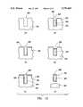
- FIGS. 1a through 1kdepict the process steps used to fill trenches formed in silicon, to which reference is now made.
- FIGS. 1a through 1kdepicts a cross-sectional view alongside a corresponding three-dimensional view.
- a bare silicon wafer 10serves as the starting substrate in a preferred form of the invention.
- waferssuch as GaAs may be used.
- a 1.5 Am thick layer of silicon oxide 12is deposited on the top surface 11 of the wafer through chemical vapor deposition (CVD).
- the silicon oxide 12may also be deposited by evaporation or can be thermally grown.
- the silicon oxide 12is covered by a photoresist layer and a lithography process is used to expose the photoresist at the desired locations of the trenches. Such processes are well known to those of skill in the art.
- the oxide 12is then patterned by dry etching (e.g. CHF 3 or CF 4 RIE) as at 13 to expose the bare silicon surface 11 where trenches will be formed, resulting in the structure depicted in FIG. 1b.
- dry etchinge.g. CHF 3 or CF 4 RIE
- an anisotropic Cl 2 RIEis then used to create a 10 ⁇ m deep trench 14 in the silicon substrate 10 at the location of pattern 13.
- An etchant having a high etch selectivity of silicon/oxideis preferred. Trenches are shaped and located depending on the features desired, as determined by the lithography step.
- the remaining oxide 12is then removed by CHF 3 RIE.
- Other etching meanscan be used such as, for example, buffered HF.
- a conformal layer approximately 1000 ⁇ thick of low temperature CVD oxide 16is next deposited to round out the sharp corners in the trenches. It should be noted that this step is recommended if spin-on-glass (SOG) will be used to fill the trenches, however, it is unnecessary if other filling mechanisms are used.
- a layer of spin-on-glass (SOG) 18is spun on at room temperature, covering oxide layer 16 and filling trench 14.
- SOGa low viscosity liquid when applied, will fill trenches whose widths are comparable to the nominal thickness of SOG on the top surface of a substrate.
- the thickness of SOG on a large open areadepends on the specific type of SOG. To fill 1 ⁇ m wide trenches, for example, a typical thickness of SOG on the base substrate would be approximately 1 ⁇ m.
- the SOGis then baked, typically on a hotplate at three temperatures, 90° C., 150° C. and 250° C. for two minutes each.
- the SOGis subsequently cured at approximately 425° C., in a convection oven for 1 hour, forming SOG oxide.
- other filling mechanismscan be used such as, for example, BPSG and PSG.
- An optional SOG layercan then be spun on to provide further planarization of the top surface of the wafer.
- a CHF 3 RIEis used to clear away SOG layer 18 and oxide layer 16 on the top surface of silicon substrate 10, leaving an exposed surface 11 and a SOG-filled trench 20.
- Micromechanical polishing or another etching mechanismmay be used, depending on the particular trench filling material.
- a chlorine RIE stepis then used to etch deeply into the silicon substrate 10 around the trench 20, to a depth of, for example, 100 microns.
- the SOG and the oxide 16block the etching of the substrate below trench 20, so that an island structure 22 is formed, comprised of CVD oxide 16, SOG 18, and silicon substrate 10.
- the SOG and oxide 16are also etched, although the SOG to silicon etch selectivity is approximately 20:1 in a C1 2 RIE.
- FIG. 1gdepicts SOG 18 and oxide 16 having a lessor height as compared to FIG. 1f.
- the island structureincludes a top 23 and sidewalls 24 and 26.
- silicon substrate 10has a new top surface 28.
- a conformal layer, approximately 3000 ⁇ thick, of low temperature CVD silicon dioxide 30is deposited on sidewalls 24, 26 and on top surface 23 and 28.
- Other conformally coated materials having a high etch selectivity over the substrate materialmay be used such as, for example, silicon nitride.
- An anisotropic etch of silicon dioxideis conducted using CHF 3 or CF 4 RIE to remove the oxide from the top surface 28 of silicon substrate 10 and from the top surface 23 of island structure 22, leaving behind a protective oxide layer 30 covering the sidewalls 24, 26.
- a chlorine RIE stepis then used to etch further down into the silicon substrate 10 to a depth of between 2 to 5 ⁇ m, leaving an extended island structure 31, as depicted in FIG. 1a.
- the top surface of the substrateis lowered, as at 28', below the side wall oxide 30, exposing the silicon forming the base 32 of the island structure.
- structure 31is released from substrate 10 by an isotropic SF 6 RIE etch which removes base silicon 32 to produce a released beam 33 which is comprised of oxide 16, SOG 18 and a core 34 of silicon.
- the beamfurther includes sidewalls 36, 38 formed from the silicon dioxide sidewall layer 30.
- the release etchextends upwardly behind the dioxide walls 36, 38 to produce an overhang below the bottom 39 of the beam, and also further lowers the surface of substrate 10, as indicated at 28".
- FIG. 1kdepicts a metal layer 40, preferably aluminum, which is sputtered over beam structure 33 to cover the top and the side walls of the beam, and to cover the surface 28" of the substrate 10.
- the metal layeris typically formed 1000 to 4000 ⁇ thick.
- FIGS. 2a to 2mdepict, in cross-section, the steps for forming SOG trench filling mask structures of different heights in a single substrate. Although any number of SOG masks of differing heights can be formed, FIGS. 2a-m specifically illustrate process steps for forming three different mask heights, through the formation of three different trench depths.
- FIGS. 2a-mspecifically illustrate process steps for forming three different mask heights, through the formation of three different trench depths.
- the processstarts with a bare silicon wafer 50 serving as a substrate and having a surface 51.
- a layer 52 of oxidesuch as silicon dioxide is deposited over the silicon substrate surface 51.
- the oxidecan be deposited by chemical vapor deposition (CVD) or evaporation or can be thermally grown.
- a first level lithographyis conducted to expose the oxide at the location (or locations) 54 of what will ultimately be the deepest trenches.
- the oxideis then patterned by dry etching, using for example CHF 3 or CF 4 RIE, at the locations of the deepest trenches.
- an etch step with a high etch selectivity of silicon to oxideis carried out to etch a trench 56 into the silicon substrate 50.
- a suitable etchantis Cl 2 RIE.
- a photoresist layer 58is next deposited and another lithography is performed to expose the silicon oxide layer 52 at the location (or locations) of what will ultimately be shallower trenches 60, as illustrated in FIG. 2c.
- the oxide 52 at the locations of the shallower trench as 60is etched away by anisotropic dry etching (CHF 3 or CF 4 RIE) (see FIG. 2d), and all photoresist is subsequently removed, resulting in the cross-section depicted in FIG. 2e.
- an etch step with a high etch selectivity of silicon to oxide(e.g. C1 2 RIE) is again done to etch into the silicon substrate 50, making trench 56 deeper and forming shallower trench 62.
- a high etch selectivity of silicon to oxidee.g. C1 2 RIE
- a third lithography stepis done to define the locations of what will ultimately be the shallowest trenches.
- a photoresist layer 64is deposited on oxide layer 52 and patterned to expose the oxide at the location (or locations) of the shallowest trench as 66.
- the oxide 52is then etched away at the locations of the shallowest trenches 66, the etch being conducted using a dry anisotropic etch as previously explained.
- all oxide 52is removed to expose substrate surface 51, by dipping the wafer into buffered hydrofluoric acid.
- Other dry etching processescan be used, for example, CHF 3 RIE. This step is optional but may be helpful in some applications. Thus, what remains are three trenches of different depths.
- SOG layer 70is spun on and subsequently baked and cured as was described with respect to FIG. 1e. Again, other filling mechanisms, such as BPSG or PSG, may be appropriate, depending upon a particular application.
- the SOG on the top silicon surface 51is then removed by an etch-back using, for example, CF 4 RIE (see FIG. 2m). Mechanical polishing may also be used to expose the bare silicon surface 51 except at the locations of the filled trenches 72, 74 and 76.
- FIGS. 3a-hdepict, in cross-section, process steps for forming SOG trench filling mask structures at a level below the top surface of a substrate.
- the process stepsare generally similar to those described previously with respect to FIGS. 1 and 2.
- the resulting filled trenches 72, 74 and 76serve as masks during subsequent etch steps to be described later.
- These filled trenchesbecome either tall, released beam structures in their own right, or serve as masks during additional deep etching into the base silicon substrate to form high aspect ratio beams. Again, these processes will be described later.
- a conformal layer of silicon dioxideis deposited on the top surface 82 of silicon substrate 84.
- the oxide layercan be deposited by evaporation or CVD, or thermally grown.
- the silicon oxideis then patterned by lithography and CHF 3 or CF 4 RIE such that the silicon substrate 84 is exposed at the area 86 where a lower level structure will be formed.
- a large open area 86is required to form a wide well. This ensures that SOG will fill the trench that will be ultimately formed at the bottom of the well defined by the open area, rather than fill the well.
- an etch step with high silicon to silicon dioxide etch selectivityis done to etch into the substrate 84 to a desired depth, forming a large trench 88.
- a layer 90 of silicon dioxideis then deposited (by CVD or evaporation) or is thermally grown, resulting in the cross-section as depicted in FIG. 3c.
- the silicon dioxide 90is then patterned by lithography and CHF 3 or CF 4 RIE to define areas 92 where trenches will be etched (FIG. 3d).
- An anisotropic etch(e.g. Cl 2 RIE) is conducted to etch deep into the substrate 84, forming trench 94, as illustrated in FIG. 3e, and the oxide layers are etched away (FIG. 3f). Thereafter, a SOG layer 96 is spun on (FIG. 3g) and subsequently baked and cured as was described with respect to the previous FIGS. 1e and 2l.
- other filling mechanismssuch as BPSG or PSG, may be appropriate, depending upon a particular application.
- the SOG on the top of silicon substrate 84is then removed by an etch-back using, for example, CF 4 RIE, resulting in SOG-filled trench 98.
- Mechanical polishingmay also be used to expose the bare silicon surface 82 except at the location of the filled trench.
- SOG filled trench 98can serve either as a released beam or as a mask during deep silicon etching to form high aspect ratio beams.
- FIGS. 2 and 3illustrate the various ways in which SOG trench fill masks can be formed.
- FIGS. 4-9depict, in cross-section, various ways in which, depending on the specific application, the mask structures can be used to form release structures. These Figures depict "post-fill-up" processes.
- SOG masks 100 and 102 of different depthsare shown in a substrate 104 after the trench filling process steps as discussed above with respect to FIGS. 2a-2m.
- an etch stepis conducted, using an isotropic etch such as SF 6 RIE to first release the SOG structure 102 (FIG. 4b) and to thereafter release SOG structure 100 (FIG. 4c).
- the released SOG structurespreferably are cantilevered, from unetched substrate adjacent the ends of the SOG beams.
- SOGalso is etched although the selectivity of silicon/SOG is about the same as that of silicon/regular silicon dioxide, which is typically approximately 20:1 in Cl 2 RIE.
- FIGS. 5a-5fgenerally depict the release of much taller (higher aspect ratio) structures.
- SOG structures 109 and 110are formed as depicted in FIG. 5a.
- An isotropic etche.g. SF 6 RIE
- an anisotropic etche.g. Chlorine RIE
- a layer 118 of oxideis conformally deposited through, for example CVD or evaporation, or thermally grown on the structures 110 and 112, as well as covering the top surface 120 of substrate 104.
- An anisotropic etch stepis then used to etch away the oxide on the top of island 112 and on substrate surface 120, thus exposing the substrate 104, FIG. 5e.
- Taller structure 122consists of SOG region 109 and silicon core region 116 bounded by oxide walls 126 and 128 formed from layer 118.
- shorter structure 124consists of SOG region 110 bounded by oxide walls 130 and 132, also formed from oxide layer 118.
- FIG. 6depicts process steps for forming two similar "tall," or high aspect ratio structures, each formed from a SOG mask having a different height than the other.
- SOG masks 140 and 142are provided in silicon substrate 144 (FIG. 6a) .
- an anisotropic etch stepis conducted to etch down into the substrate to form island structures 146 and 148.
- Each islandconsists of a SOG region, 140 and 142 respectively, over a region of silicon, 150 and 152 respectively.
- a conformal layer of oxide 154is deposited or thermally grown on both islands, and an anisotropic etch (e.g.
- CF 4 RIECF 4 RIE
- An optional anisotropic etch using, for example, chlorine RIE, followed by an isotropic etch using, for example, SF 6 RIE,are then conducted, forming released beam structures 156 and 158 extending over the floor 155' of substrate 144.
- FIGS. 7a-7hdepict process steps for producing a released solid structure and a released structure consisting only of sidewalls.
- FIGS. 7a-7fare essentially the same as those shown in FIGS. 6a-6f, and as such they will not be described. These steps result in the released beam structures 160 and 162 depicted in FIG. 7f.
- Each of these structuresincludes a SOG region, 164 and 166 respectively; a silicon core region, 168 and 170 respectively; and sidewalls 172 and 174, respectively.
- An anisotropic oxide etche.g., CF 4 RIE
- CF 4 RIEanisotropic oxide etch
- FIGS. 8a-8iillustrate a process for fabrication of SOG released beams having multiple side wall layers and being of different aspect ratios.
- an anisotropic etchis conducted around SOG masks 180 and 182 to etch down into the substrate 104, leaving the bottom of SOG mask 180 below the surface 184 of substrate 104 (FIG. 8b) and forming island structure 183.
- a conformal layer 186 of oxideis then deposited or thermally grown on the substrate, on mask 180, and on island 183. This is followed by an anisotropic etch that removes the oxide 186 from the surface 184 and from the tops of masks 180 and 182. Referring to FIG.
- an isotropic etche.g. SF 6 RIE
- SOG mask 180is not released at this stage, but instead forms an island having sidewalls 198 bounding only the SOG region 180.
- An anisotropic etche.g., Chlorine RIE
- Island structure 200consists of SOG region 180, including sidewalls 198, atop a core silicon region 202.
- the island 200 and beam 190 structuresare then coated by a conformal layer of oxide 204. Thereafter, the oxide 204 is etched away from the surface 206 of substrate 104 and from the tops of structures 190 and 200 by an anisotropic oxide etch (e.g., CF 4 RIE), as illustrated in FIG. 8h. Finally, referring to FIG. 8i, the island structure 200 is released from the substrate 104 by an isotropic etch with a high etch selectivity of substrate to oxide (e.g., SF 6 RIE) to provide a released beam.
- CF 4 RIEanisotropic oxide etch
- FIGS. 9a-9gAnother configuration for released beams fabricated utilizing the above-described SOG masking process is illustrated in FIGS. 9a-9g, wherein beams having differently sized interior, or core, structures but similar oxide sidewalls are provided.
- an anisotropic etch stepis conducted to etch down into the substrate around SOG masks 220 and 222, as has been described previously, to produce island 223.
- etch depthis controlled such that the bottom 224 of the SOG trench-filling mask 220 remains below the top surface 226 of substrate 104.
- Island 223includes SOG mask 222 and underlying silicon region 227, as previously described with respect to FIGS. 7b and 8b. As depicted in FIG.
- a conformal layer of oxide 230is then deposited or thermally grown over the entire structure, and an anisotropic etch (e.g., Cl 2 RIE) is then conducted to remove the oxide 230 from the surface 226 of substrate 104 and from the tops of SOG mask 220 and island 223 (see FIG. 9d).
- an isotropic etche.g. SF 6 RIE
- isotropic etchis then used to release island structure 223 beneath sidewalls 236 formed from layer 230 and bounding SOG region 222 and underlying silicon region 227 to produce released beam 238.
- An anisotropic etch(e.g., Chlorine RIE) is then conducted to etch deep into the substrate 104, resulting in the island structure 240 depicted in FIG. 9f and including SOG mask 220 and underlying core structure 241.
- an isotropic etch(e.g., SF 6 RIE) is conducted to release the island structure 240, to produce released beam 242 having oxide sidewalls 244 formed from layer 230. Since sidewalls 236 and 244 were formed by layer 230 when the underlying mask 220 and island 222 were at the same height (FIG. 9d), the sidewalls also are of the same height, even though the underlying SOG mask 220 in beam 242 is of a different height than the underlying SOG mask 222 and core 227 in beam 238.
- a layer of metal such as aluminumcan be sputtered onto the structures depicted in FIGS. 4c, 5f, 6f, 7h, 8i and 9g.
- This metalcovers the sidewalls of the structures nearly conformally, typically to a thickness of approximately 0.2 ⁇ m, and was illustrated with respect to the description of FIG. 1.
- SOGcan be removed by using either a dry etching step using, for example, CHF 3 or CF 4 RIE. This etching also etches silicon. Or, a buffered hydrofluoric acid (BHF) can be used to remove the SOG without attacking the silicon beams.
- BHFbuffered hydrofluoric acid
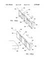
- FIGS. 10 and 11illustrate an application of the present invention in the forming of a linear ultra-high aspect ratio comb-type micro-actuator.
- FIG. 10is a top plan view of the basic structure of an electrostatic comb actuator 250, depicting a movable fingers element 252 and a fixed fingers element 254.
- the fingersare conductive, or are covered by conductive layers, so that when appropriate potential differences are applied between the fixed and movable fingers, relative movement is produced.
- Figs. 11a-11gdepict a 3-D, cutaway view of a comb actuator formed using the present inventive process.
- the process steps used to form the actuatorinclude steps described with respect to FIGS. 1, 2 and 3.
- Fig. 11aillustrates at 256 a "masking trench" design for the actuator of FIG. 10, in a cutaway view, depicting shallow trench 260, and deeper trenches 262, 263 formed in a silicon substrate 264 having a top surface 265.
- These trenchesare formed at different depths in the manner as described previously with reference to FIGS. 2 and 3.
- trenches 262 and 263are formed at the bottom of wells 266 and 267 as described with respect to FIG. 3.
- the trenchescan be formed closely spaced together, for example 3 to 6 ⁇ m apart.
- the trenchescan be formed to a variety of depths, for example 5 ⁇ m deep for shallow trench 260, and approximately 10 ⁇ m for deeper trenches 262 and 263, measured from the bottom of 1-3 ⁇ m deep wells 266 and 267.
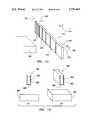
- FIG. 11bdepicts the deposition of SOG layer 268 to a depth of 4 ⁇ m on the top surface of substrate 264.
- the SOGfills each of the trenches 260, 262 and 263, but does not fill wells 266 and 267 during the spin-on process.
- the SOG layeris etched from the top surface of substrate 264, leaving trenches 260, 262 and 263 filled with SOG.
- a layer of CVD silicon dioxide 270 approximately 1.5-2 ⁇ m thickis then deposited and patterned on the top surface 265 of silicon substrate 264.
- the oxide layercontacts shallow trench 262 at 272.
- the oxide layerwill be formed into a spring/anchor structure 274 having a released spring portion 276 approximately 5-10 ⁇ m wide and 100-1000 ⁇ m long, and an anchor portion 277.
- FIG. 11edepicts the partially exposed beams 278, 279 and 280, and released spring 276 resulting from an isotropic RIE into the silicon substrate 264.
- the isotropic etchusing SF 6 for example, is used to etch approximately 3-6 ⁇ m into the substrate, exposing the beams and releasing the spring 276. Due to the size of the anchor region, it is not released as a result of the etch process, but rather, it sits upon island 282.
- an anisotropic RIEusing Cl 2 for example, is used to vertically etch approximately 5 ⁇ m further into the silicon substrate, further increasing the exposed height of beams 278, 279 and 280.
- beam 278is now formed with a top SOG region 284 and a bottom region 285, still attached to substrate 264.
- Beams 279 and 280, formed entirely of SOG,are also still attached to the substrate 264.
- Anchor 277stands atop a taller island 286.
- FIG. 11gdepicts a final actuator structure 250.
- a layer of CVD oxide 288 approximately 0.2 ⁇ m thickis conformally deposited, followed by an anisotropic RIE to etch the oxide 288, exposing silicon as described with respect to FIGS. 1h and 1i.
- an isotropic RIE etchusing for example SF 6 , is done to release the moveable fingers 290 attached to spring 276 in the manner described with respect to FIG. 1j. It is worth noting that the fixed fingers 291 and 292 stay unreleased.
- a layer of metalsuch as, for example, Aluminum, approximately 0.2 ⁇ m thick is sputtered to form a metallization layer 289 overlaying the movable 290 and fixed fingers 291 and 292, as well as the spring 276 and anchor 277 and the base substrate 264, in a manner similar to that described with respect to FIG. 1k.
- FIG. 12a-12fdepict a method for fabricating a movable waveguide structure using the SOG mask process of the invention.
- a waveguideis typically composed of a core and a cladding.
- the present inventioncan be used to form a released, movable, waveguide having a core formed from SOG or some other trench filling material.
- the claddingincludes a thin layer at the bottom of the trench, a sidewall layer and a layer on top. These layers can be deposited dielectrics or metals depending on the specific design.
- the use of SOGis advantageous due to the low temperatures used in the process and SOG's compatibility with various substrates. This last aspect is particularly desirable in optical waveguide structures since it is advantageous to form the optical waveguide on the same chip with a fabricated semiconductor laser.
- FIG. 12aillustrates the formation of a trench 300 in a silicon substrate 302.
- a conformal silicon nitride layer 304is deposited, FIG. 12b, and trench 300 is filled with SOG 306, as has been described previously, FIG. 12c.
- an oxide etch backis conducted using, for example, CF 4 RIE, to remove oxide from the top of substrate 302 and from the top portion 307 of trench 300.
- a suitable waveguide material 308is evaporated onto the structure, and finally, as depicted in FIG. 12f, the structure 310 is released by SF 6 RIE, resulting in a movable waveguide structure.
- FIGS. 13a and billustrate an in-plane movable, variable (spatial) period optical grating 320, fabricated using the SOG trench filling mask process of the present invention.
- the XY actuators for moving the gratingare not shown.
- FIG. 13adepicts a masking trench definition for the device, including the depiction of shallower trenches 322 and 324, as well as deeper trenches 326, 328 and 330. These trenches were formed in the manner as described with respect to FIG. 2.
- Lines 332 and 334illustrate the directions for connection to X actuators for moving grating 320 along an x axis
- lines 336 and 338indicate the directions for connection to Y actuators for moving the grating along a y axis
- Directional arrow 340indicates that the device can be connected to rotational actuators.
- FIG. 13billustrates the grating structure 320 after fabrication of elements in the trenches of FIG. 13a, and after their release, as described above.
- the gratingis integrated with an on-chip semiconductor laser 350, and further includes transparent oxide regions 352, 354 and 356, as well as opaque, silicon regions 358 and 360.
- the oxide regionsare the SOG trench-filling material in trenches 326, 328 and 330, respectively.
- FIG. 14illustrates a released optical grating 370 having a varied spatial period.
- Grating lines 372are silicon material between transparent SOG oxide regions, and vary in density across the face of the grating 370, being less dense in region 374 and more dense in region 376. Thus, moving the grating in the X direction will vary the period of the grating with respect to laser 350.
- FIGS. 15a and 15billustrate a high aspect ratio released structure having a smooth bottom.
- the structureis formed without the need for a thick layer deposition.
- FIGS. 15a (a cross-section view) and 15b (a three dimensional view)illustrate only the last step in the process since the previous steps are exactly as those shown in FIGS. 1a-f.
- An SF 6 RIEis used to release the structure 380 from the silicon substrate 382.
- the structurehas a SOG interior 384, bounded on it's sides 386 and bottom 388 by a CVD oxide layer, resulting in a very smooth bottom surface 388 on the structure.
- the present inventive trench-filling etch masking micro-fabrication techniqueopens up a tremendous area of exciting new applications. It utilizes the novel concept of using materials to fill up trenches which then serve as etch masks, allowing the formation of microstructures with topologies impractical using conventional technologies.
- the inventive processis a low temperature, low stress process resulting in ultra-high aspect ratio (100-200:1) structures.
- ultra-high aspect ratio structurescan be formed, each level independently controlled.
- three dimensional linear actuatorscan be fabricated by following simple steps based on the present novel technique.
- ultra-high aspect ratio XYZ flexure structurescan be formed without the need for complex lithography steps.
Landscapes
- Engineering & Computer Science (AREA)
- Manufacturing & Machinery (AREA)
- Microelectronics & Electronic Packaging (AREA)
- Physics & Mathematics (AREA)
- Geometry (AREA)
- Micromachines (AREA)
- Drying Of Semiconductors (AREA)
Abstract
Description
Claims (6)
Priority Applications (1)
| Application Number | Priority Date | Filing Date | Title |
|---|---|---|---|
| US08/668,378US5770465A (en) | 1995-06-23 | 1996-06-21 | Trench-filling etch-masking microfabrication technique |
Applications Claiming Priority (2)
| Application Number | Priority Date | Filing Date | Title |
|---|---|---|---|
| US43995P | 1995-06-23 | 1995-06-23 | |
| US08/668,378US5770465A (en) | 1995-06-23 | 1996-06-21 | Trench-filling etch-masking microfabrication technique |
Publications (1)
| Publication Number | Publication Date |
|---|---|
| US5770465Atrue US5770465A (en) | 1998-06-23 |
Family
ID=26667635
Family Applications (1)
| Application Number | Title | Priority Date | Filing Date |
|---|---|---|---|
| US08/668,378Expired - LifetimeUS5770465A (en) | 1995-06-23 | 1996-06-21 | Trench-filling etch-masking microfabrication technique |
Country Status (1)
| Country | Link |
|---|---|
| US (1) | US5770465A (en) |
Cited By (37)
| Publication number | Priority date | Publication date | Assignee | Title |
|---|---|---|---|---|
| US6020272A (en)* | 1998-10-08 | 2000-02-01 | Sandia Corporation | Method for forming suspended micromechanical structures |
| WO1999036941A3 (en)* | 1998-01-15 | 2000-02-10 | Cornell Res Foundation Inc | Trench isolation for micromechanical devices |
| US6180536B1 (en)* | 1998-06-04 | 2001-01-30 | Cornell Research Foundation, Inc. | Suspended moving channels and channel actuators for microfluidic applications and method for making |
| US6251248B1 (en)* | 1999-10-15 | 2001-06-26 | Ching-Bin Lin | Microfabrication process for making microstructures having high aspect ratio |
| US6277756B1 (en)* | 1999-02-12 | 2001-08-21 | Denso Corporation | Method for manufacturing semiconductor device |
| DE10021489C2 (en)* | 1999-10-20 | 2002-03-28 | Lin Ching Bin | Microfabrication process for the production of microstructures with a large aspect ratio |
| US6402301B1 (en) | 2000-10-27 | 2002-06-11 | Lexmark International, Inc | Ink jet printheads and methods therefor |
| AU749702B2 (en)* | 1998-09-08 | 2002-07-04 | Commonwealth Scientific And Industrial Research Organisation | Three-dimensional microstructure |
| US20020113034A1 (en)* | 1999-06-16 | 2002-08-22 | Kionix, Inc. | Methods of fabricating microelectromechanical and microfluidic devices |
| US20020136518A1 (en)* | 2001-03-21 | 2002-09-26 | Wang Everett X. | Fabrication of optical waveguides for reduction of minimum waveguide spacing |
| US20030044106A1 (en)* | 2001-07-24 | 2003-03-06 | Chuang-Chia Lin | Mems element having perpendicular portion formed from substrate |
| US6544863B1 (en) | 2001-08-21 | 2003-04-08 | Calient Networks, Inc. | Method of fabricating semiconductor wafers having multiple height subsurface layers |
| US6563106B1 (en) | 2000-02-01 | 2003-05-13 | Calient Networks, Inc. | Micro-electro-mechanical-system (MEMS) mirror device and methods for fabricating the same |
| US6571628B1 (en) | 2000-10-16 | 2003-06-03 | Institute Of Microelectronics | Z-axis accelerometer |
| US6583031B2 (en) | 2001-07-25 | 2003-06-24 | Onix Microsystems, Inc. | Method of making a MEMS element having perpendicular portion formed from substrate |
| US6599842B2 (en)* | 1999-11-29 | 2003-07-29 | Applied Materials, Inc. | Method for rounding corners and removing damaged outer surfaces of a trench |
| US20030161069A1 (en)* | 2002-02-27 | 2003-08-28 | Seagate Technology, Llc | Wafer-level fabrication method for top or side slider bond pads |
| US6624077B2 (en) | 2001-12-17 | 2003-09-23 | Applied Materials, Inc. | Integrated circuit waveguide |
| US6628041B2 (en) | 2000-05-16 | 2003-09-30 | Calient Networks, Inc. | Micro-electro-mechanical-system (MEMS) mirror device having large angle out of plane motion using shaped combed finger actuators and method for fabricating the same |
| US20040094800A1 (en)* | 2001-01-15 | 2004-05-20 | Fairchild Korea Semiconductor Ltd. | High voltage semiconductor device having high breakdown voltage and method of fabricating the same |
| US6753638B2 (en) | 2000-02-03 | 2004-06-22 | Calient Networks, Inc. | Electrostatic actuator for micromechanical systems |
| US20040161576A1 (en)* | 2003-02-14 | 2004-08-19 | Hiroyuki Yoshimura | Method of manufacturing master disc for magnetic transfer, a master disc thereof, and a master disc formed thereby |
| US20040198063A1 (en)* | 2002-06-27 | 2004-10-07 | Kanakasabapathi Subramanian | Three dimensional high aspect ratio micromachining |
| US6819820B1 (en) | 2000-11-29 | 2004-11-16 | Analog Devices, Inc. | Use of applied force to improve MEMS switch performance |
| US6825967B1 (en) | 2000-09-29 | 2004-11-30 | Calient Networks, Inc. | Shaped electrodes for micro-electro-mechanical-system (MEMS) devices to improve actuator performance and methods for fabricating the same |
| WO2004014785A3 (en)* | 2002-08-05 | 2005-02-10 | Univ Kassel | Method for producing at least one small opening in a layer on a substrate and components produced according to said method |
| US6887391B1 (en)* | 2000-03-24 | 2005-05-03 | Analog Devices, Inc. | Fabrication and controlled release of structures using etch-stop trenches |
| US20050153506A1 (en)* | 2004-01-13 | 2005-07-14 | Yinan Chen | Isolation structure for trench capacitors and fabrication method thereof |
| US20050199013A1 (en)* | 2004-03-12 | 2005-09-15 | Applied Materials, Inc. | Use of amorphous carbon film as a hardmask in the fabrication of optical waveguides |
| US20080138987A1 (en)* | 2004-11-26 | 2008-06-12 | Applied Materials, Inc. | Edge removal of silicon-on-insulator transfer wafer |
| US7728339B1 (en) | 2002-05-03 | 2010-06-01 | Calient Networks, Inc. | Boundary isolation for microelectromechanical devices |
| US20120092771A1 (en)* | 2010-10-18 | 2012-04-19 | International Business Machines Corporation | Embedded vertical optical grating for heterogeneous integration |
| US20130233824A1 (en)* | 2012-01-01 | 2013-09-12 | Acacia Communications Inc. | Low-loss, wide-band grating coupler and method of making same |
| US20150087092A1 (en)* | 2013-04-22 | 2015-03-26 | Empire Technology Development Llc | Opto-mechanical alignment |
| US20170365507A1 (en)* | 2012-07-25 | 2017-12-21 | Infineon Technologies Ag | Field Emission Devices and Methods of Making Thereof |
| JP2018531803A (en)* | 2015-09-30 | 2018-11-01 | メムズ ドライブ, インク.Mems Drive, Inc. | Simplified MEMS device manufacturing process |
| US12103843B2 (en) | 2021-01-20 | 2024-10-01 | Calient.Ai Inc. | MEMS mirror arrays with reduced crosstalk |
Citations (11)
| Publication number | Priority date | Publication date | Assignee | Title |
|---|---|---|---|---|
| US4968585A (en)* | 1989-06-20 | 1990-11-06 | The Board Of Trustees Of The Leland Stanford Jr. University | Microfabricated cantilever stylus with integrated conical tip |
| DE4000496A1 (en)* | 1989-08-17 | 1991-02-21 | Bosch Gmbh Robert | METHOD FOR STRUCTURING A SEMICONDUCTOR BODY |
| US5256592A (en)* | 1989-10-20 | 1993-10-26 | Oki Electric Industry Co., Ltd. | Method for fabricating a semiconductor integrated circuit device |
| US5273939A (en)* | 1991-03-09 | 1993-12-28 | Robert Bosch Gmbh | Method of assembling micromechanical sensors |
| US5296092A (en)* | 1992-01-16 | 1994-03-22 | Samsung Electronics Co., Ltd. | Planarization method for a semiconductor substrate |
| US5306659A (en)* | 1993-03-29 | 1994-04-26 | International Business Machines Corporation | Reach-through isolation etching method for silicon-on-insulator devices |
| US5316979A (en)* | 1992-01-16 | 1994-05-31 | Cornell Research Foundation, Inc. | RIE process for fabricating submicron, silicon electromechanical structures |
| US5324683A (en)* | 1993-06-02 | 1994-06-28 | Motorola, Inc. | Method of forming a semiconductor structure having an air region |
| US5372968A (en)* | 1993-09-27 | 1994-12-13 | United Microelectronics Corporation | Planarized local oxidation by trench-around technology |
| US5393375A (en)* | 1992-02-03 | 1995-02-28 | Cornell Research Foundation, Inc. | Process for fabricating submicron single crystal electromechanical structures |
| US5407860A (en)* | 1994-05-27 | 1995-04-18 | Texas Instruments Incorporated | Method of forming air gap dielectric spaces between semiconductor leads |
- 1996
- 1996-06-21USUS08/668,378patent/US5770465A/ennot_activeExpired - Lifetime
Patent Citations (11)
| Publication number | Priority date | Publication date | Assignee | Title |
|---|---|---|---|---|
| US4968585A (en)* | 1989-06-20 | 1990-11-06 | The Board Of Trustees Of The Leland Stanford Jr. University | Microfabricated cantilever stylus with integrated conical tip |
| DE4000496A1 (en)* | 1989-08-17 | 1991-02-21 | Bosch Gmbh Robert | METHOD FOR STRUCTURING A SEMICONDUCTOR BODY |
| US5256592A (en)* | 1989-10-20 | 1993-10-26 | Oki Electric Industry Co., Ltd. | Method for fabricating a semiconductor integrated circuit device |
| US5273939A (en)* | 1991-03-09 | 1993-12-28 | Robert Bosch Gmbh | Method of assembling micromechanical sensors |
| US5296092A (en)* | 1992-01-16 | 1994-03-22 | Samsung Electronics Co., Ltd. | Planarization method for a semiconductor substrate |
| US5316979A (en)* | 1992-01-16 | 1994-05-31 | Cornell Research Foundation, Inc. | RIE process for fabricating submicron, silicon electromechanical structures |
| US5393375A (en)* | 1992-02-03 | 1995-02-28 | Cornell Research Foundation, Inc. | Process for fabricating submicron single crystal electromechanical structures |
| US5306659A (en)* | 1993-03-29 | 1994-04-26 | International Business Machines Corporation | Reach-through isolation etching method for silicon-on-insulator devices |
| US5324683A (en)* | 1993-06-02 | 1994-06-28 | Motorola, Inc. | Method of forming a semiconductor structure having an air region |
| US5372968A (en)* | 1993-09-27 | 1994-12-13 | United Microelectronics Corporation | Planarized local oxidation by trench-around technology |
| US5407860A (en)* | 1994-05-27 | 1995-04-18 | Texas Instruments Incorporated | Method of forming air gap dielectric spaces between semiconductor leads |
Cited By (73)
| Publication number | Priority date | Publication date | Assignee | Title |
|---|---|---|---|---|
| WO1999036941A3 (en)* | 1998-01-15 | 2000-02-10 | Cornell Res Foundation Inc | Trench isolation for micromechanical devices |
| US6180536B1 (en)* | 1998-06-04 | 2001-01-30 | Cornell Research Foundation, Inc. | Suspended moving channels and channel actuators for microfluidic applications and method for making |
| AU749702B2 (en)* | 1998-09-08 | 2002-07-04 | Commonwealth Scientific And Industrial Research Organisation | Three-dimensional microstructure |
| US6020272A (en)* | 1998-10-08 | 2000-02-01 | Sandia Corporation | Method for forming suspended micromechanical structures |
| US6277756B1 (en)* | 1999-02-12 | 2001-08-21 | Denso Corporation | Method for manufacturing semiconductor device |
| US6969470B2 (en) | 1999-06-16 | 2005-11-29 | Kionix, Inc. | Method for fabricating ESI device using smile and delayed LOCOS techniques |
| US6824697B2 (en) | 1999-06-16 | 2004-11-30 | Kionix, Inc. | Method for fabricating mems and microfluidic devices using smile, latent masking, and delayed locos techniques |
| US6780336B2 (en) | 1999-06-16 | 2004-08-24 | James E. Moon | Methods of fabricating MEMS and microfluidic devices using latent masking technique |
| US20020113034A1 (en)* | 1999-06-16 | 2002-08-22 | Kionix, Inc. | Methods of fabricating microelectromechanical and microfluidic devices |
| US6444138B1 (en)* | 1999-06-16 | 2002-09-03 | James E. Moon | Method of fabricating microelectromechanical and microfluidic devices |
| US6706200B2 (en) | 1999-06-16 | 2004-03-16 | Kionix, Inc. | Method for fabricating ESI device using smile and delayed LOCOS techniques |
| US6464892B2 (en) | 1999-06-16 | 2002-10-15 | James E. Moon | Methods of fabricating microelectromechanical and microfluidic devices |
| US6913701B2 (en) | 1999-06-16 | 2005-07-05 | Kionix, Inc. | Method for fabricating integrated LC/ESI device using SMILE, latent masking, and delayed LOCOS techniques |
| US6702950B2 (en) | 1999-06-16 | 2004-03-09 | James E. Moon | Method for fabricating LC device using latent masking and delayed LOCOS techniques |
| US20040082088A1 (en)* | 1999-06-16 | 2004-04-29 | Kionix, Inc. | Method for fabricating ESI device using smile and delayed LOCOS techniques |
| US20040079723A1 (en)* | 1999-06-16 | 2004-04-29 | Moon James E. | Method for fabricating integrated LC/ESI device using SMILE,latent masking, and delayed LOCOS techniques |
| US6673253B2 (en) | 1999-06-16 | 2004-01-06 | Kionix, Inc. | Method of fabricating integrated LC/ESI device using smile, latent masking, and delayed locos techniques. |
| US6251248B1 (en)* | 1999-10-15 | 2001-06-26 | Ching-Bin Lin | Microfabrication process for making microstructures having high aspect ratio |
| DE10021489C2 (en)* | 1999-10-20 | 2002-03-28 | Lin Ching Bin | Microfabrication process for the production of microstructures with a large aspect ratio |
| US6599842B2 (en)* | 1999-11-29 | 2003-07-29 | Applied Materials, Inc. | Method for rounding corners and removing damaged outer surfaces of a trench |
| US6563106B1 (en) | 2000-02-01 | 2003-05-13 | Calient Networks, Inc. | Micro-electro-mechanical-system (MEMS) mirror device and methods for fabricating the same |
| US6753638B2 (en) | 2000-02-03 | 2004-06-22 | Calient Networks, Inc. | Electrostatic actuator for micromechanical systems |
| US20040246306A1 (en)* | 2000-02-03 | 2004-12-09 | Scott Adams | Electrostatic actuator for microelectromechanical systems and methods of fabrication |
| US7098571B2 (en) | 2000-02-03 | 2006-08-29 | Calient Networks, Inc. | Electrostatic actuator for microelectromechanical systems and methods of fabrication |
| US7261826B2 (en) | 2000-02-03 | 2007-08-28 | Calient Networks, Inc. | Electrostatic actuator for microelectromechanical systems and methods of fabrication |
| US6887391B1 (en)* | 2000-03-24 | 2005-05-03 | Analog Devices, Inc. | Fabrication and controlled release of structures using etch-stop trenches |
| US6628041B2 (en) | 2000-05-16 | 2003-09-30 | Calient Networks, Inc. | Micro-electro-mechanical-system (MEMS) mirror device having large angle out of plane motion using shaped combed finger actuators and method for fabricating the same |
| US6825967B1 (en) | 2000-09-29 | 2004-11-30 | Calient Networks, Inc. | Shaped electrodes for micro-electro-mechanical-system (MEMS) devices to improve actuator performance and methods for fabricating the same |
| US6662654B2 (en) | 2000-10-16 | 2003-12-16 | Institute Of Microelectronics | Z-axis accelerometer |
| US6571628B1 (en) | 2000-10-16 | 2003-06-03 | Institute Of Microelectronics | Z-axis accelerometer |
| US6402301B1 (en) | 2000-10-27 | 2002-06-11 | Lexmark International, Inc | Ink jet printheads and methods therefor |
| US20040247237A1 (en)* | 2000-11-29 | 2004-12-09 | Murali Chaparala | Use of applied force to improve mems switch performance |
| US6888979B2 (en) | 2000-11-29 | 2005-05-03 | Analog Devices, Inc. | MEMS mirrors with precision clamping mechanism |
| US6819820B1 (en) | 2000-11-29 | 2004-11-16 | Analog Devices, Inc. | Use of applied force to improve MEMS switch performance |
| US7129542B2 (en)* | 2001-01-15 | 2006-10-31 | Fairchild Korea Semiconductor Ltd. | High voltage semiconductor device having high breakdown voltage and method of fabricating the same |
| US20040094800A1 (en)* | 2001-01-15 | 2004-05-20 | Fairchild Korea Semiconductor Ltd. | High voltage semiconductor device having high breakdown voltage and method of fabricating the same |
| US20020136518A1 (en)* | 2001-03-21 | 2002-09-26 | Wang Everett X. | Fabrication of optical waveguides for reduction of minimum waveguide spacing |
| US7039288B2 (en)* | 2001-03-21 | 2006-05-02 | Intel Corporation | Fabrication of optical waveguides for reduction of minimum waveguide spacing |
| US6813412B2 (en) | 2001-07-24 | 2004-11-02 | Michael J. Daneman | Mems element having perpendicular portion formed from substrate |
| US20030044106A1 (en)* | 2001-07-24 | 2003-03-06 | Chuang-Chia Lin | Mems element having perpendicular portion formed from substrate |
| US6583031B2 (en) | 2001-07-25 | 2003-06-24 | Onix Microsystems, Inc. | Method of making a MEMS element having perpendicular portion formed from substrate |
| US6544863B1 (en) | 2001-08-21 | 2003-04-08 | Calient Networks, Inc. | Method of fabricating semiconductor wafers having multiple height subsurface layers |
| US6624077B2 (en) | 2001-12-17 | 2003-09-23 | Applied Materials, Inc. | Integrated circuit waveguide |
| US7254885B2 (en)* | 2002-02-27 | 2007-08-14 | Seagate Technology, Llc | Wafer-level fabrication method for top or side slider bond pads |
| US20030161069A1 (en)* | 2002-02-27 | 2003-08-28 | Seagate Technology, Llc | Wafer-level fabrication method for top or side slider bond pads |
| US7728339B1 (en) | 2002-05-03 | 2010-06-01 | Calient Networks, Inc. | Boundary isolation for microelectromechanical devices |
| US7504757B2 (en) | 2002-06-27 | 2009-03-17 | Cornell Research Foundation, Inc. | Multi-finger z-actuator |
| US7045466B2 (en) | 2002-06-27 | 2006-05-16 | Cornell Research Foundation, Inc. | Three dimensional high aspect ratio micromachining |
| US20060157807A1 (en)* | 2002-06-27 | 2006-07-20 | Cornell Research Foundation, Inc. | Three dimensional high aspect ratio micromachining |
| US20040198063A1 (en)* | 2002-06-27 | 2004-10-07 | Kanakasabapathi Subramanian | Three dimensional high aspect ratio micromachining |
| US20060165957A1 (en)* | 2002-08-05 | 2006-07-27 | Egbert Oesterschulze | Method for producing at least one small opening in a layer on a substrate and components produced according ot said method |
| WO2004014785A3 (en)* | 2002-08-05 | 2005-02-10 | Univ Kassel | Method for producing at least one small opening in a layer on a substrate and components produced according to said method |
| US20040161576A1 (en)* | 2003-02-14 | 2004-08-19 | Hiroyuki Yoshimura | Method of manufacturing master disc for magnetic transfer, a master disc thereof, and a master disc formed thereby |
| US7041567B2 (en)* | 2004-01-13 | 2006-05-09 | Nanya Technology Corp. | Isolation structure for trench capacitors and fabrication method thereof |
| US20050151182A1 (en)* | 2004-01-13 | 2005-07-14 | Yi-Nan Chen | Isolation structure for trench capacitors and fabrication method thereof |
| US20050153506A1 (en)* | 2004-01-13 | 2005-07-14 | Yinan Chen | Isolation structure for trench capacitors and fabrication method thereof |
| US20050199013A1 (en)* | 2004-03-12 | 2005-09-15 | Applied Materials, Inc. | Use of amorphous carbon film as a hardmask in the fabrication of optical waveguides |
| US7079740B2 (en) | 2004-03-12 | 2006-07-18 | Applied Materials, Inc. | Use of amorphous carbon film as a hardmask in the fabrication of optical waveguides |
| US20090061545A1 (en)* | 2004-11-26 | 2009-03-05 | Applied Materials, Inc. | Edge Removal Of Silicon-On-Insulator Transfer Wafer |
| US20080138987A1 (en)* | 2004-11-26 | 2008-06-12 | Applied Materials, Inc. | Edge removal of silicon-on-insulator transfer wafer |
| EP1662560A3 (en)* | 2004-11-26 | 2009-07-22 | Applied Materials, Inc. | Edge removal of silicon-on-insulator transfer wafer |
| US7749908B2 (en) | 2004-11-26 | 2010-07-06 | S.O.I.Tec Silicon On Insulator Technologies | Edge removal of silicon-on-insulator transfer wafer |
| US7951718B2 (en) | 2004-11-26 | 2011-05-31 | Applied Materials, Inc. | Edge removal of silicon-on-insulator transfer wafer |
| US8767299B2 (en)* | 2010-10-18 | 2014-07-01 | International Business Machines Corporation | Embedded vertical optical grating for heterogeneous integration |
| US20120092771A1 (en)* | 2010-10-18 | 2012-04-19 | International Business Machines Corporation | Embedded vertical optical grating for heterogeneous integration |
| US20130233824A1 (en)* | 2012-01-01 | 2013-09-12 | Acacia Communications Inc. | Low-loss, wide-band grating coupler and method of making same |
| US8883018B2 (en)* | 2012-01-01 | 2014-11-11 | Acacia Communications Inc. | Low-loss, wide-band grating coupler and method of making same |
| US20170365507A1 (en)* | 2012-07-25 | 2017-12-21 | Infineon Technologies Ag | Field Emission Devices and Methods of Making Thereof |
| US10504772B2 (en)* | 2012-07-25 | 2019-12-10 | Infineon Technologies Ag | Field emission devices and methods of making thereof |
| US20150087092A1 (en)* | 2013-04-22 | 2015-03-26 | Empire Technology Development Llc | Opto-mechanical alignment |
| US9252321B2 (en)* | 2013-04-22 | 2016-02-02 | Empire Technology Development Llc | Opto-mechanical alignment |
| JP2018531803A (en)* | 2015-09-30 | 2018-11-01 | メムズ ドライブ, インク.Mems Drive, Inc. | Simplified MEMS device manufacturing process |
| US12103843B2 (en) | 2021-01-20 | 2024-10-01 | Calient.Ai Inc. | MEMS mirror arrays with reduced crosstalk |
Similar Documents
| Publication | Publication Date | Title |
|---|---|---|
| US5770465A (en) | Trench-filling etch-masking microfabrication technique | |
| US7504757B2 (en) | Multi-finger z-actuator | |
| US5846849A (en) | Microstructure and single mask, single-crystal process for fabrication thereof | |
| US5316979A (en) | RIE process for fabricating submicron, silicon electromechanical structures | |
| US6586841B1 (en) | Mechanical landing pad formed on the underside of a MEMS device | |
| DE60128437T2 (en) | Method for producing micromechanical and microoptomechanical structures with backside metallization | |
| DE60128529T2 (en) | Process for the production of micromechanical and microoptomechanical structures with exposure of monocrystalline silicon | |
| US6808952B1 (en) | Process for fabricating a microelectromechanical structure | |
| US20130012024A1 (en) | Structure for microelectronics and microsystem and manufacturing process | |
| US6887391B1 (en) | Fabrication and controlled release of structures using etch-stop trenches | |
| US6884732B2 (en) | Method of fabricating a device having a desired non-planar surface or profile and device produced thereby | |
| Sniegowski | Chemical-mechanical polishing: enhancing the manufacturability of MEMS | |
| WO2008016985A2 (en) | Fabrication of an integrated terahertz source using field emitter array with grating structure | |
| US6472332B1 (en) | Surface micromachined structure fabrication methods for a fluid ejection device | |
| US6613243B2 (en) | Method of making a 3-D structure using an erodable mask formed from a film having a composition that varies in its direction of thickness | |
| DE60128440T2 (en) | Method for producing micromechanical and microoptomechanical structures with an applied pattern | |
| Hofmann et al. | Monolithic three-dimensional single-crystal silicon microelectromechanical systems | |
| JP2006015440A (en) | Method of manufacturing semiconductor structure |
Legal Events
| Date | Code | Title | Description |
|---|---|---|---|
| AS | Assignment | Owner name:CORNELL RESEARCH FOUNDATION, INC., NEW YORK Free format text:ASSIGNMENT OF ASSIGNORS INTEREST;ASSIGNORS:MACDONALD, NOEL C.;HUANG, XIAOJUN TRENT;CHEN, LIANG-YUH;REEL/FRAME:008150/0789;SIGNING DATES FROM 19960823 TO 19960906 | |
| STCF | Information on status: patent grant | Free format text:PATENTED CASE | |
| FEPP | Fee payment procedure | Free format text:PAT HLDR NO LONGER CLAIMS SMALL ENT STAT AS NONPROFIT ORG (ORIGINAL EVENT CODE: LSM3); ENTITY STATUS OF PATENT OWNER: LARGE ENTITY | |
| REFU | Refund | Free format text:REFUND - PAYMENT OF MAINTENANCE FEE, 4TH YR, SMALL ENTITY (ORIGINAL EVENT CODE: R283); ENTITY STATUS OF PATENT OWNER: LARGE ENTITY | |
| AS | Assignment | Owner name:VENTURE LENDING & LEASING III, INC., AS AGENT, CAL Free format text:SECURITY AGREEMENT;ASSIGNOR:CALIENT OPTICAL COMPONENTS, INC.;REEL/FRAME:011934/0464 Effective date:20010516 | |
| FPAY | Fee payment | Year of fee payment:4 | |
| AS | Assignment | Owner name:PENTECH FINANCIAL SERVICES, INC., CALIFORNIA Free format text:SECURITY INTEREST;ASSIGNOR:CALIENT OPTICAL COMPONENTS, INC.;REEL/FRAME:012252/0175 Effective date:20010516 | |
| AS | Assignment | Owner name:DARPA, VIRGINIA Free format text:CONFIRMATORY LICENSE;ASSIGNOR:CORNELL RESEARCH FOUNDATION, INC.;REEL/FRAME:012875/0957 Effective date:20020423 | |
| AS | Assignment | Owner name:CALIENT OPTICAL COMPONENTS, INC., NEW YORK Free format text:RELEASE AGREEMENT;ASSIGNORS:VENTURE LENDING;LEASING III, INC.;REEL/FRAME:016172/0341 Effective date:20040825 Owner name:CALIENT OPTICAL COMPONENTS, INC., NEW YORK Free format text:RELEASE AGREEMENT;ASSIGNOR:PENTECH FINANCIAL SERVICES, INC.;REEL/FRAME:016182/0031 Effective date:20040831 | |
| FPAY | Fee payment | Year of fee payment:8 | |
| FEPP | Fee payment procedure | Free format text:PAYOR NUMBER ASSIGNED (ORIGINAL EVENT CODE: ASPN); ENTITY STATUS OF PATENT OWNER: LARGE ENTITY | |
| FPAY | Fee payment | Year of fee payment:12 | |
| REMI | Maintenance fee reminder mailed | ||
| SULP | Surcharge for late payment | Year of fee payment:11 | |
| AS | Assignment | Owner name:CALIENT HOLDINGS, LLC, CALIFORNIA Free format text:SECURITY INTEREST;ASSIGNOR:CALIENT TECHNOLOGIES, INC.;REEL/FRAME:044914/0972 Effective date:20171215 | |
| AS | Assignment | Owner name:CALIENT TECHNOLOGIES, INC., CALIFORNIA Free format text:RELEASE BY SECURED PARTY;ASSIGNOR:CALIENT HOLDINGS, LLC;REEL/FRAME:053251/0224 Effective date:20200720 |