US5769989A - Method and system for reworkable direct chip attach (DCA) structure with thermal enhancement - Google Patents
Method and system for reworkable direct chip attach (DCA) structure with thermal enhancementDownload PDFInfo
- Publication number
- US5769989A US5769989AUS08/530,452US53045295AUS5769989AUS 5769989 AUS5769989 AUS 5769989AUS 53045295 AUS53045295 AUS 53045295AUS 5769989 AUS5769989 AUS 5769989A
- Authority
- US
- United States
- Prior art keywords
- carrier board
- integrated circuit
- circuit device
- solder
- solder layer
- Prior art date
- Legal status (The legal status is an assumption and is not a legal conclusion. Google has not performed a legal analysis and makes no representation as to the accuracy of the status listed.)
- Expired - Lifetime
Links
- 238000000034methodMethods0.000titleclaimsdescription20
- 229910000679solderInorganic materials0.000claimsabstractdescription58
- 239000010410layerSubstances0.000claimsabstractdescription39
- 239000012790adhesive layerSubstances0.000claimsabstractdescription16
- 239000000853adhesiveSubstances0.000description15
- 230000001070adhesive effectEffects0.000description15
- 239000000463materialSubstances0.000description7
- 239000002184metalSubstances0.000description7
- 230000000712assemblyEffects0.000description4
- 238000000429assemblyMethods0.000description4
- 238000005476solderingMethods0.000description4
- 230000015572biosynthetic processEffects0.000description3
- 230000002950deficientEffects0.000description3
- VYPSYNLAJGMNEJ-UHFFFAOYSA-NSilicium dioxideChemical compoundO=[Si]=OVYPSYNLAJGMNEJ-UHFFFAOYSA-N0.000description2
- 239000011248coating agentSubstances0.000description2
- 238000000576coating methodMethods0.000description2
- 238000002844meltingMethods0.000description2
- 230000008018meltingEffects0.000description2
- 239000000126substanceSubstances0.000description2
- 239000004642PolyimideSubstances0.000description1
- ATJFFYVFTNAWJD-UHFFFAOYSA-NTinChemical compound[Sn]ATJFFYVFTNAWJD-UHFFFAOYSA-N0.000description1
- 229910045601alloyInorganic materials0.000description1
- 239000000956alloySubstances0.000description1
- 238000005219brazingMethods0.000description1
- 239000000919ceramicSubstances0.000description1
- 238000004140cleaningMethods0.000description1
- 230000007547defectEffects0.000description1
- 238000011161developmentMethods0.000description1
- 229910003460diamondInorganic materials0.000description1
- 239000010432diamondSubstances0.000description1
- 238000004100electronic packagingMethods0.000description1
- 239000010408filmSubstances0.000description1
- 239000007788liquidSubstances0.000description1
- 238000004519manufacturing processMethods0.000description1
- 239000002923metal particleSubstances0.000description1
- 238000013021overheatingMethods0.000description1
- 239000002245particleSubstances0.000description1
- 239000004033plasticSubstances0.000description1
- 229920001721polyimidePolymers0.000description1
- 230000005855radiationEffects0.000description1
- 230000009257reactivityEffects0.000description1
- 238000012216screeningMethods0.000description1
- 239000000377silicon dioxideSubstances0.000description1
- 239000002904solventSubstances0.000description1
- 238000010561standard procedureMethods0.000description1
- 238000003860storageMethods0.000description1
- 239000000758substrateSubstances0.000description1
- 239000010409thin filmSubstances0.000description1
- 239000012808vapor phaseSubstances0.000description1
Images

Classifications
- H—ELECTRICITY
- H01—ELECTRIC ELEMENTS
- H01L—SEMICONDUCTOR DEVICES NOT COVERED BY CLASS H10
- H01L24/00—Arrangements for connecting or disconnecting semiconductor or solid-state bodies; Methods or apparatus related thereto
- H01L24/80—Methods for connecting semiconductor or other solid state bodies using means for bonding being attached to, or being formed on, the surface to be connected
- H01L24/83—Methods for connecting semiconductor or other solid state bodies using means for bonding being attached to, or being formed on, the surface to be connected using a layer connector
- H—ELECTRICITY
- H01—ELECTRIC ELEMENTS
- H01L—SEMICONDUCTOR DEVICES NOT COVERED BY CLASS H10
- H01L24/00—Arrangements for connecting or disconnecting semiconductor or solid-state bodies; Methods or apparatus related thereto
- H01L24/01—Means for bonding being attached to, or being formed on, the surface to be connected, e.g. chip-to-package, die-attach, "first-level" interconnects; Manufacturing methods related thereto
- H01L24/26—Layer connectors, e.g. plate connectors, solder or adhesive layers; Manufacturing methods related thereto
- H01L24/31—Structure, shape, material or disposition of the layer connectors after the connecting process
- H01L24/32—Structure, shape, material or disposition of the layer connectors after the connecting process of an individual layer connector
- H—ELECTRICITY
- H05—ELECTRIC TECHNIQUES NOT OTHERWISE PROVIDED FOR
- H05K—PRINTED CIRCUITS; CASINGS OR CONSTRUCTIONAL DETAILS OF ELECTRIC APPARATUS; MANUFACTURE OF ASSEMBLAGES OF ELECTRICAL COMPONENTS
- H05K1/00—Printed circuits
- H05K1/02—Details
- H05K1/0201—Thermal arrangements, e.g. for cooling, heating or preventing overheating
- H05K1/0203—Cooling of mounted components
- H05K1/0204—Cooling of mounted components using means for thermal conduction connection in the thickness direction of the substrate
- H05K1/0206—Cooling of mounted components using means for thermal conduction connection in the thickness direction of the substrate by printed thermal vias
- H—ELECTRICITY
- H01—ELECTRIC ELEMENTS
- H01L—SEMICONDUCTOR DEVICES NOT COVERED BY CLASS H10
- H01L2224/00—Indexing scheme for arrangements for connecting or disconnecting semiconductor or solid-state bodies and methods related thereto as covered by H01L24/00
- H01L2224/01—Means for bonding being attached to, or being formed on, the surface to be connected, e.g. chip-to-package, die-attach, "first-level" interconnects; Manufacturing methods related thereto
- H01L2224/26—Layer connectors, e.g. plate connectors, solder or adhesive layers; Manufacturing methods related thereto
- H01L2224/31—Structure, shape, material or disposition of the layer connectors after the connecting process
- H01L2224/32—Structure, shape, material or disposition of the layer connectors after the connecting process of an individual layer connector
- H01L2224/321—Disposition
- H01L2224/32151—Disposition the layer connector connecting between a semiconductor or solid-state body and an item not being a semiconductor or solid-state body, e.g. chip-to-substrate, chip-to-passive
- H01L2224/32221—Disposition the layer connector connecting between a semiconductor or solid-state body and an item not being a semiconductor or solid-state body, e.g. chip-to-substrate, chip-to-passive the body and the item being stacked
- H01L2224/32225—Disposition the layer connector connecting between a semiconductor or solid-state body and an item not being a semiconductor or solid-state body, e.g. chip-to-substrate, chip-to-passive the body and the item being stacked the item being non-metallic, e.g. insulating substrate with or without metallisation
- H—ELECTRICITY
- H01—ELECTRIC ELEMENTS
- H01L—SEMICONDUCTOR DEVICES NOT COVERED BY CLASS H10
- H01L2224/00—Indexing scheme for arrangements for connecting or disconnecting semiconductor or solid-state bodies and methods related thereto as covered by H01L24/00
- H01L2224/01—Means for bonding being attached to, or being formed on, the surface to be connected, e.g. chip-to-package, die-attach, "first-level" interconnects; Manufacturing methods related thereto
- H01L2224/42—Wire connectors; Manufacturing methods related thereto
- H01L2224/47—Structure, shape, material or disposition of the wire connectors after the connecting process
- H01L2224/48—Structure, shape, material or disposition of the wire connectors after the connecting process of an individual wire connector
- H01L2224/4805—Shape
- H01L2224/4809—Loop shape
- H01L2224/48091—Arched
- H—ELECTRICITY
- H01—ELECTRIC ELEMENTS
- H01L—SEMICONDUCTOR DEVICES NOT COVERED BY CLASS H10
- H01L2224/00—Indexing scheme for arrangements for connecting or disconnecting semiconductor or solid-state bodies and methods related thereto as covered by H01L24/00
- H01L2224/01—Means for bonding being attached to, or being formed on, the surface to be connected, e.g. chip-to-package, die-attach, "first-level" interconnects; Manufacturing methods related thereto
- H01L2224/42—Wire connectors; Manufacturing methods related thereto
- H01L2224/47—Structure, shape, material or disposition of the wire connectors after the connecting process
- H01L2224/48—Structure, shape, material or disposition of the wire connectors after the connecting process of an individual wire connector
- H01L2224/481—Disposition
- H01L2224/48151—Connecting between a semiconductor or solid-state body and an item not being a semiconductor or solid-state body, e.g. chip-to-substrate, chip-to-passive
- H01L2224/48221—Connecting between a semiconductor or solid-state body and an item not being a semiconductor or solid-state body, e.g. chip-to-substrate, chip-to-passive the body and the item being stacked
- H01L2224/48225—Connecting between a semiconductor or solid-state body and an item not being a semiconductor or solid-state body, e.g. chip-to-substrate, chip-to-passive the body and the item being stacked the item being non-metallic, e.g. insulating substrate with or without metallisation
- H01L2224/48227—Connecting between a semiconductor or solid-state body and an item not being a semiconductor or solid-state body, e.g. chip-to-substrate, chip-to-passive the body and the item being stacked the item being non-metallic, e.g. insulating substrate with or without metallisation connecting the wire to a bond pad of the item
- H—ELECTRICITY
- H01—ELECTRIC ELEMENTS
- H01L—SEMICONDUCTOR DEVICES NOT COVERED BY CLASS H10
- H01L2224/00—Indexing scheme for arrangements for connecting or disconnecting semiconductor or solid-state bodies and methods related thereto as covered by H01L24/00
- H01L2224/73—Means for bonding being of different types provided for in two or more of groups H01L2224/10, H01L2224/18, H01L2224/26, H01L2224/34, H01L2224/42, H01L2224/50, H01L2224/63, H01L2224/71
- H01L2224/732—Location after the connecting process
- H01L2224/73251—Location after the connecting process on different surfaces
- H01L2224/73265—Layer and wire connectors
- H—ELECTRICITY
- H01—ELECTRIC ELEMENTS
- H01L—SEMICONDUCTOR DEVICES NOT COVERED BY CLASS H10
- H01L2224/00—Indexing scheme for arrangements for connecting or disconnecting semiconductor or solid-state bodies and methods related thereto as covered by H01L24/00
- H01L2224/80—Methods for connecting semiconductor or other solid state bodies using means for bonding being attached to, or being formed on, the surface to be connected
- H01L2224/83—Methods for connecting semiconductor or other solid state bodies using means for bonding being attached to, or being formed on, the surface to be connected using a layer connector
- H01L2224/8319—Arrangement of the layer connectors prior to mounting
- H—ELECTRICITY
- H01—ELECTRIC ELEMENTS
- H01L—SEMICONDUCTOR DEVICES NOT COVERED BY CLASS H10
- H01L2224/00—Indexing scheme for arrangements for connecting or disconnecting semiconductor or solid-state bodies and methods related thereto as covered by H01L24/00
- H01L2224/80—Methods for connecting semiconductor or other solid state bodies using means for bonding being attached to, or being formed on, the surface to be connected
- H01L2224/83—Methods for connecting semiconductor or other solid state bodies using means for bonding being attached to, or being formed on, the surface to be connected using a layer connector
- H01L2224/838—Bonding techniques
- H01L2224/83801—Soldering or alloying
- H—ELECTRICITY
- H01—ELECTRIC ELEMENTS
- H01L—SEMICONDUCTOR DEVICES NOT COVERED BY CLASS H10
- H01L2924/00—Indexing scheme for arrangements or methods for connecting or disconnecting semiconductor or solid-state bodies as covered by H01L24/00
- H01L2924/01—Chemical elements
- H01L2924/01006—Carbon [C]
- H—ELECTRICITY
- H01—ELECTRIC ELEMENTS
- H01L—SEMICONDUCTOR DEVICES NOT COVERED BY CLASS H10
- H01L2924/00—Indexing scheme for arrangements or methods for connecting or disconnecting semiconductor or solid-state bodies as covered by H01L24/00
- H01L2924/01—Chemical elements
- H01L2924/01013—Aluminum [Al]
- H—ELECTRICITY
- H01—ELECTRIC ELEMENTS
- H01L—SEMICONDUCTOR DEVICES NOT COVERED BY CLASS H10
- H01L2924/00—Indexing scheme for arrangements or methods for connecting or disconnecting semiconductor or solid-state bodies as covered by H01L24/00
- H01L2924/01—Chemical elements
- H01L2924/01027—Cobalt [Co]
- H—ELECTRICITY
- H01—ELECTRIC ELEMENTS
- H01L—SEMICONDUCTOR DEVICES NOT COVERED BY CLASS H10
- H01L2924/00—Indexing scheme for arrangements or methods for connecting or disconnecting semiconductor or solid-state bodies as covered by H01L24/00
- H01L2924/01—Chemical elements
- H01L2924/01033—Arsenic [As]
- H—ELECTRICITY
- H01—ELECTRIC ELEMENTS
- H01L—SEMICONDUCTOR DEVICES NOT COVERED BY CLASS H10
- H01L2924/00—Indexing scheme for arrangements or methods for connecting or disconnecting semiconductor or solid-state bodies as covered by H01L24/00
- H01L2924/01—Chemical elements
- H01L2924/0105—Tin [Sn]
- H—ELECTRICITY
- H01—ELECTRIC ELEMENTS
- H01L—SEMICONDUCTOR DEVICES NOT COVERED BY CLASS H10
- H01L2924/00—Indexing scheme for arrangements or methods for connecting or disconnecting semiconductor or solid-state bodies as covered by H01L24/00
- H01L2924/01—Chemical elements
- H01L2924/01079—Gold [Au]
- H—ELECTRICITY
- H01—ELECTRIC ELEMENTS
- H01L—SEMICONDUCTOR DEVICES NOT COVERED BY CLASS H10
- H01L2924/00—Indexing scheme for arrangements or methods for connecting or disconnecting semiconductor or solid-state bodies as covered by H01L24/00
- H01L2924/01—Chemical elements
- H01L2924/01082—Lead [Pb]
- H—ELECTRICITY
- H01—ELECTRIC ELEMENTS
- H01L—SEMICONDUCTOR DEVICES NOT COVERED BY CLASS H10
- H01L2924/00—Indexing scheme for arrangements or methods for connecting or disconnecting semiconductor or solid-state bodies as covered by H01L24/00
- H01L2924/013—Alloys
- H01L2924/014—Solder alloys
- H—ELECTRICITY
- H01—ELECTRIC ELEMENTS
- H01L—SEMICONDUCTOR DEVICES NOT COVERED BY CLASS H10
- H01L2924/00—Indexing scheme for arrangements or methods for connecting or disconnecting semiconductor or solid-state bodies as covered by H01L24/00
- H01L2924/06—Polymers
- H01L2924/078—Adhesive characteristics other than chemical
- H—ELECTRICITY
- H01—ELECTRIC ELEMENTS
- H01L—SEMICONDUCTOR DEVICES NOT COVERED BY CLASS H10
- H01L2924/00—Indexing scheme for arrangements or methods for connecting or disconnecting semiconductor or solid-state bodies as covered by H01L24/00
- H01L2924/10—Details of semiconductor or other solid state devices to be connected
- H01L2924/11—Device type
- H01L2924/14—Integrated circuits
- H—ELECTRICITY
- H05—ELECTRIC TECHNIQUES NOT OTHERWISE PROVIDED FOR
- H05K—PRINTED CIRCUITS; CASINGS OR CONSTRUCTIONAL DETAILS OF ELECTRIC APPARATUS; MANUFACTURE OF ASSEMBLAGES OF ELECTRICAL COMPONENTS
- H05K1/00—Printed circuits
- H05K1/02—Details
- H05K1/0201—Thermal arrangements, e.g. for cooling, heating or preventing overheating
- H05K1/0212—Printed circuits or mounted components having integral heating means
- H—ELECTRICITY
- H05—ELECTRIC TECHNIQUES NOT OTHERWISE PROVIDED FOR
- H05K—PRINTED CIRCUITS; CASINGS OR CONSTRUCTIONAL DETAILS OF ELECTRIC APPARATUS; MANUFACTURE OF ASSEMBLAGES OF ELECTRICAL COMPONENTS
- H05K2201/00—Indexing scheme relating to printed circuits covered by H05K1/00
- H05K2201/09—Shape and layout
- H05K2201/09209—Shape and layout details of conductors
- H05K2201/095—Conductive through-holes or vias
- H05K2201/09572—Solder filled plated through-hole in the final product
- H—ELECTRICITY
- H05—ELECTRIC TECHNIQUES NOT OTHERWISE PROVIDED FOR
- H05K—PRINTED CIRCUITS; CASINGS OR CONSTRUCTIONAL DETAILS OF ELECTRIC APPARATUS; MANUFACTURE OF ASSEMBLAGES OF ELECTRICAL COMPONENTS
- H05K2203/00—Indexing scheme relating to apparatus or processes for manufacturing printed circuits covered by H05K3/00
- H05K2203/04—Soldering or other types of metallurgic bonding
- H05K2203/049—Wire bonding
- H—ELECTRICITY
- H05—ELECTRIC TECHNIQUES NOT OTHERWISE PROVIDED FOR
- H05K—PRINTED CIRCUITS; CASINGS OR CONSTRUCTIONAL DETAILS OF ELECTRIC APPARATUS; MANUFACTURE OF ASSEMBLAGES OF ELECTRICAL COMPONENTS
- H05K2203/00—Indexing scheme relating to apparatus or processes for manufacturing printed circuits covered by H05K3/00
- H05K2203/17—Post-manufacturing processes
- H05K2203/176—Removing, replacing or disconnecting component; Easily removable component
- H—ELECTRICITY
- H05—ELECTRIC TECHNIQUES NOT OTHERWISE PROVIDED FOR
- H05K—PRINTED CIRCUITS; CASINGS OR CONSTRUCTIONAL DETAILS OF ELECTRIC APPARATUS; MANUFACTURE OF ASSEMBLAGES OF ELECTRICAL COMPONENTS
- H05K3/00—Apparatus or processes for manufacturing printed circuits
- H05K3/30—Assembling printed circuits with electric components, e.g. with resistor
- H05K3/32—Assembling printed circuits with electric components, e.g. with resistor electrically connecting electric components or wires to printed circuits
- H05K3/34—Assembling printed circuits with electric components, e.g. with resistor electrically connecting electric components or wires to printed circuits by soldering
- H05K3/341—Surface mounted components
- H—ELECTRICITY
- H05—ELECTRIC TECHNIQUES NOT OTHERWISE PROVIDED FOR
- H05K—PRINTED CIRCUITS; CASINGS OR CONSTRUCTIONAL DETAILS OF ELECTRIC APPARATUS; MANUFACTURE OF ASSEMBLAGES OF ELECTRICAL COMPONENTS
- H05K3/00—Apparatus or processes for manufacturing printed circuits
- H05K3/40—Forming printed elements for providing electric connections to or between printed circuits
- H05K3/42—Plated through-holes or plated via connections
- H05K3/429—Plated through-holes specially for multilayer circuits, e.g. having connections to inner circuit layers
- Y—GENERAL TAGGING OF NEW TECHNOLOGICAL DEVELOPMENTS; GENERAL TAGGING OF CROSS-SECTIONAL TECHNOLOGIES SPANNING OVER SEVERAL SECTIONS OF THE IPC; TECHNICAL SUBJECTS COVERED BY FORMER USPC CROSS-REFERENCE ART COLLECTIONS [XRACs] AND DIGESTS
- Y10—TECHNICAL SUBJECTS COVERED BY FORMER USPC
- Y10S—TECHNICAL SUBJECTS COVERED BY FORMER USPC CROSS-REFERENCE ART COLLECTIONS [XRACs] AND DIGESTS
- Y10S156/00—Adhesive bonding and miscellaneous chemical manufacture
- Y10S156/934—Apparatus having delaminating means adapted for delaminating a specified article
- Y10S156/941—Means for delaminating semiconductive product
- Y—GENERAL TAGGING OF NEW TECHNOLOGICAL DEVELOPMENTS; GENERAL TAGGING OF CROSS-SECTIONAL TECHNOLOGIES SPANNING OVER SEVERAL SECTIONS OF THE IPC; TECHNICAL SUBJECTS COVERED BY FORMER USPC CROSS-REFERENCE ART COLLECTIONS [XRACs] AND DIGESTS
- Y10—TECHNICAL SUBJECTS COVERED BY FORMER USPC
- Y10S—TECHNICAL SUBJECTS COVERED BY FORMER USPC CROSS-REFERENCE ART COLLECTIONS [XRACs] AND DIGESTS
- Y10S428/00—Stock material or miscellaneous articles
- Y10S428/901—Printed circuit
- Y—GENERAL TAGGING OF NEW TECHNOLOGICAL DEVELOPMENTS; GENERAL TAGGING OF CROSS-SECTIONAL TECHNOLOGIES SPANNING OVER SEVERAL SECTIONS OF THE IPC; TECHNICAL SUBJECTS COVERED BY FORMER USPC CROSS-REFERENCE ART COLLECTIONS [XRACs] AND DIGESTS
- Y10—TECHNICAL SUBJECTS COVERED BY FORMER USPC
- Y10T—TECHNICAL SUBJECTS COVERED BY FORMER US CLASSIFICATION
- Y10T156/00—Adhesive bonding and miscellaneous chemical manufacture
- Y10T156/19—Delaminating means
- Y—GENERAL TAGGING OF NEW TECHNOLOGICAL DEVELOPMENTS; GENERAL TAGGING OF CROSS-SECTIONAL TECHNOLOGIES SPANNING OVER SEVERAL SECTIONS OF THE IPC; TECHNICAL SUBJECTS COVERED BY FORMER USPC CROSS-REFERENCE ART COLLECTIONS [XRACs] AND DIGESTS
- Y10—TECHNICAL SUBJECTS COVERED BY FORMER USPC
- Y10T—TECHNICAL SUBJECTS COVERED BY FORMER US CLASSIFICATION
- Y10T29/00—Metal working
- Y10T29/49—Method of mechanical manufacture
- Y10T29/49718—Repairing
- Y10T29/49721—Repairing with disassembling
- Y10T29/4973—Replacing of defective part
- Y—GENERAL TAGGING OF NEW TECHNOLOGICAL DEVELOPMENTS; GENERAL TAGGING OF CROSS-SECTIONAL TECHNOLOGIES SPANNING OVER SEVERAL SECTIONS OF THE IPC; TECHNICAL SUBJECTS COVERED BY FORMER USPC CROSS-REFERENCE ART COLLECTIONS [XRACs] AND DIGESTS
- Y10—TECHNICAL SUBJECTS COVERED BY FORMER USPC
- Y10T—TECHNICAL SUBJECTS COVERED BY FORMER US CLASSIFICATION
- Y10T428/00—Stock material or miscellaneous articles
- Y10T428/31504—Composite [nonstructural laminate]
- Y10T428/31678—Of metal
- Y10T428/31681—Next to polyester, polyamide or polyimide [e.g., alkyd, glue, or nylon, etc.]
Definitions
- the present inventionrelates to surface mounting operations in general, and in particular to a method and system for surface mounting electronic circuit assemblies. Still more particularly, the present invention relates to a method and system for surface mounting electronic circuit assemblies to allow easy removal of any wire-bonded surface-mounted integrated circuits on a carrier board.
- DCAdirect chip attach
- the surface-mounted circuit assemblyhas four layers, namely, an integrated circuit device, an adhesive layer, the solder layer and the carrier board.
- the integrated circuit deviceis removably attached to a solder layer which is disposed on top of the carrier board, with an adhesive layer disposed between the integrated device and the solder layer.
- the carrier boardincludes at least one aperture or "via" disposed beneath the location where the integrated circuit device is to be mounted.
- the viais filled with solder such that the solder layer upon which the integrated circuit device is situated is thermo-conductively connected to the back side of the carrier board. This configuration allows an integrated circuit device to be easily removed from the carrier board by the local application of heat to the back side of the carrier board.
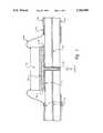
- FIG. 1is a cross-sectional view of a surface-mounted circuit assembly according to the preferred embodiment of the present invention.
- FIG. 2is an alternative embodiment of the present invention in which a multiple number of vias is used.
- FIG. 1illustrates an integrated circuit device 10 which is mounted to a carrier board 40.
- carrier board 40typically includes metal traces 42, device mounting pad 43, wirebondable overplate layers 44 (such as Au over Ni), and a solder mask 46.
- a metal-coated via 50is provided through carrier board 40.
- the metal-coated via 50is located beneath integrated circuit device 10 and is electrically and thermally connected to device mounting pad 43.
- integrated circuit device 10is also electrically connected to wirebondable overplate layers 44 through metal bondwires 48.
- a solder layer 30is disposed on the pad site of integrated circuit device 10 by a solder application process such as wave soldering or application of solder paste to the solder pad.
- a solder application processsuch as wave soldering or application of solder paste to the solder pad.
- the solderflows through via 50 and subsequently coats an even layer of solder on the device pad of integrated circuit device 10 to form the solder layer 30.
- solder paste processthe addition of solder involves standard techniques such as stencilling or screening solder paste followed by vapor-phase reflow, or reflow by infrared radiation, hot air, or a hot plate. The subsequent reflow of solder paste results in the formation of a solder coating on a device pad.
- via 50is filled with solder such that the solder layer 30 is electrically and thermally connected to the back side of the carrier board 40.
- An integrated circuit device 10is then applied to the solder layer 30 with an adhesive layer 20.
- integrated circuit device 10thereafter, should integrated circuit device 10 become defective for any reason, it can be dislodged, after the removal of metal bondwires 48, by simply applying heat locally to the back side of the carrier board 40 at which via 50 is located.
- the integrated circuit device 10 along with the adhesive layer 20can easily be removed from the surface of the carrier board 40.
- the removal of the defective integrated circuit device 10may be accomplished by lifting the device 10 away from the carrier board 40 with a specific device-handler (not shown).
- adhesive layer 20is of a non-meltable nature, it will stay adhered to the bottom side of the integrated circuit device 10 as the integrated device 10 is being lifted away, without leaving any residue behind. Hence, the device site is ready to use without additional cleaning or redressing. Furthermore, because heat is only applied locally to the via, there is no potential risk of damaging the defective device site or the adjacent sites due to overheating.
- Solder layer 30may be a layer of ordinary solder, a special type of solder such as lead-free, a brazing alloy, or any other substance compatible with the carrier board material and the wiring.
- the melting temperature of the substance used as solder layer 30must exceed the normal operating temperature of the circuit assembly, and must be low enough that it can flow and reflow without damaging the material of the carrier board; melting temperature is typically in the range of 100° C. to 400° C.
- Solder layer 30normally covers device pad areas in the range of 2-25mm on a side, and has a conventional thickness of approximately 0.001-0.25mm. The thickness of the solder layer is determined by known considerations such as metal reactivity and adequate liquid film formation for subsequent device removal.
- a variety of adhesivescan be used as adhesive layer 20.
- the adhesive materialmay be thermally conductive or insulative, as well as electrically conductive or insulative. However, the adhesive material need not be heat-softenable in order to provide rework capability. This allows the use of some adhesive materials which sacrifice softenability or tearability in order to achieve higher bond strength or other desirable properties.
- Electrically insulating adhesivescan be made electrically conductive by impregnating them with metal particles. Otherwise, electrically insulating adhesives can be made thermally conductive by impregnating them with particles of diamond, BN, AIN, silica, ZnO, etc. Examples of adhesive materials that can be used as adhesive layer 20 are electrically conductive AblestikTM 84-LMI or electrically/thermally insulative AblestikTM 84-3.
- a multiple number of viascan be used at the device sites throughout the carrier board 40.
- three vias 52are shown to be used underneath integrated circuit device 10.
- a solder layer 30is disposed on the pad site of integrated circuit device 10 by a solder application process such as wave soldering or application of solder paste to the solder pad.
- the solderflows through vias 52 and subsequently coats an even layer of solder on the device pad of integrated circuit device 10 to form the solder layer 30.
- solder paste processthe subsequent reflow of solder paste results in the formation of a solder coating on a device pad.
- solder layer 30is electrically and thermally connected to the back side of the carrier board 40.
- the integrated circuit device 10is subsequently attached to solder layer 30 with an adhesive layer 20 in between the integrated circuit device 10 and solder layer 30.
- This surface-mounted circuit assembly configurationprovides a reworkable structure for efficient and cost effective device removal and replacement. Furthermore, the vias also provide an in-service thermal enhancement to the integrated circuit devices on the carrier board.
- the present inventionis applicable to all wirebonding technology, where the integrated circuit devices are wirebonded to either a variety of substrate materials (such as FR4, polyimide, ceramic, metal and thin film) or leadframes as is in the case for most plastic packages such as SOIC, PQFP, PLCC, DIP, etc.
- substrate materialssuch as FR4, polyimide, ceramic, metal and thin film
- leadframesas is in the case for most plastic packages such as SOIC, PQFP, PLCC, DIP, etc.
- the concepts under the present inventioncould also be used to provide reworkability for any electrical component interconnections with the use of conductive adhesives as well. This may become extremely important in future applications when the use of lead-free systems are of primary concern in environmentally conscious products. For example, leaded components could be bonded to pads on a carrier board coated with a tin based leadfree solder with a conductive adhesive similar to those used for wirebonded integrated circuit attach. The fusible lead-free solder on the pad surface could then be melted to allow for reworkability of the adhesive attached component leads.
- the present inventionalso possesses a broad range of applicability within the realm of electronic packaging well beyond the use for rework of wirebonded integrated circuit devices.
Landscapes
- Engineering & Computer Science (AREA)
- Microelectronics & Electronic Packaging (AREA)
- Computer Hardware Design (AREA)
- Power Engineering (AREA)
- Electric Connection Of Electric Components To Printed Circuits (AREA)
Abstract
Description
Claims (7)
Priority Applications (1)
| Application Number | Priority Date | Filing Date | Title |
|---|---|---|---|
| US08/530,452US5769989A (en) | 1995-09-19 | 1995-09-19 | Method and system for reworkable direct chip attach (DCA) structure with thermal enhancement |
Applications Claiming Priority (1)
| Application Number | Priority Date | Filing Date | Title |
|---|---|---|---|
| US08/530,452US5769989A (en) | 1995-09-19 | 1995-09-19 | Method and system for reworkable direct chip attach (DCA) structure with thermal enhancement |
Publications (1)
| Publication Number | Publication Date |
|---|---|
| US5769989Atrue US5769989A (en) | 1998-06-23 |
Family
ID=24113687
Family Applications (1)
| Application Number | Title | Priority Date | Filing Date |
|---|---|---|---|
| US08/530,452Expired - LifetimeUS5769989A (en) | 1995-09-19 | 1995-09-19 | Method and system for reworkable direct chip attach (DCA) structure with thermal enhancement |
Country Status (1)
| Country | Link |
|---|---|
| US (1) | US5769989A (en) |
Cited By (34)
| Publication number | Priority date | Publication date | Assignee | Title |
|---|---|---|---|---|
| US6084775A (en)* | 1998-12-09 | 2000-07-04 | International Business Machines Corporation | Heatsink and package structures with fusible release layer |
| US6156150A (en)* | 1996-04-16 | 2000-12-05 | Matsushita Electric Industrial Co., Ltd. | IC component separating method and separating apparatus |
| US6253675B1 (en) | 1999-06-29 | 2001-07-03 | Carl P. Mayer | Solder paste stenciling apparatus and method of use for rework |
| US6605868B2 (en)* | 1998-12-10 | 2003-08-12 | Kabushiki Kaisha Toshiba | Insulating substrate including multilevel insulative ceramic layers joined with an intermediate layer |
| US6715203B2 (en)* | 2000-02-18 | 2004-04-06 | Eupec Europaeische Gesellschaft Fuer Leistungshalbleiter Mbh & Co. Kg | Substrate for power semiconductor modules with through-plating of solder and method for its production |
| US20040111854A1 (en)* | 2001-12-18 | 2004-06-17 | Rikiya Kamimura | Method and appratus of recycling printed circuit board |
| US6905914B1 (en)* | 2002-11-08 | 2005-06-14 | Amkor Technology, Inc. | Wafer level package and fabrication method |
| US20050133574A1 (en)* | 2003-12-19 | 2005-06-23 | Hispano Suiza | Process for soldering an electronic component on an electronic card, process for repairing the card and installation for using the process |
| WO2007039330A1 (en)* | 2005-09-30 | 2007-04-12 | Siemens Aktiengesellschaft | Printed board and method for producing the same |
| US20070181640A1 (en)* | 2006-02-03 | 2007-08-09 | Quanta Computer Inc. | Lead-free solder reworking system and method thereof |
| US7361533B1 (en) | 2002-11-08 | 2008-04-22 | Amkor Technology, Inc. | Stacked embedded leadframe |
| US7572681B1 (en) | 2005-12-08 | 2009-08-11 | Amkor Technology, Inc. | Embedded electronic component package |
| US20100061056A1 (en)* | 2008-09-08 | 2010-03-11 | Damion Searls | Mainboard assembly including a package overlying a die directly attached to the mainboard |
| US7723210B2 (en) | 2002-11-08 | 2010-05-25 | Amkor Technology, Inc. | Direct-write wafer level chip scale package |
| US7902660B1 (en) | 2006-05-24 | 2011-03-08 | Amkor Technology, Inc. | Substrate for semiconductor device and manufacturing method thereof |
| US20110091640A1 (en)* | 2008-10-17 | 2011-04-21 | Samsung Electro-Mechanics Co., Ltd. | Non-shrinking ceramic substrate and method of manufacturing the same |
| US20110205719A1 (en)* | 2010-02-24 | 2011-08-25 | Atsushi Watanabe | Electronic component |
| US20110242765A1 (en)* | 2010-03-31 | 2011-10-06 | Hong Kong Applied Science and Technology Research Institute Company Limited | Semiconductor package and method of manufacturing the same |
| US8294276B1 (en) | 2010-05-27 | 2012-10-23 | Amkor Technology, Inc. | Semiconductor device and fabricating method thereof |
| US8324511B1 (en) | 2010-04-06 | 2012-12-04 | Amkor Technology, Inc. | Through via nub reveal method and structure |
| US8390130B1 (en) | 2011-01-06 | 2013-03-05 | Amkor Technology, Inc. | Through via recessed reveal structure and method |
| US20130099388A1 (en)* | 2011-10-21 | 2013-04-25 | Hynix Semiconductor Inc. | Stacked semiconductor package |
| US8440554B1 (en) | 2010-08-02 | 2013-05-14 | Amkor Technology, Inc. | Through via connected backside embedded circuit features structure and method |
| US8487445B1 (en) | 2010-10-05 | 2013-07-16 | Amkor Technology, Inc. | Semiconductor device having through electrodes protruding from dielectric layer |
| US8552548B1 (en) | 2011-11-29 | 2013-10-08 | Amkor Technology, Inc. | Conductive pad on protruding through electrode semiconductor device |
| US8791501B1 (en) | 2010-12-03 | 2014-07-29 | Amkor Technology, Inc. | Integrated passive device structure and method |
| US8796561B1 (en) | 2009-10-05 | 2014-08-05 | Amkor Technology, Inc. | Fan out build up substrate stackable package and method |
| WO2014124272A2 (en) | 2013-02-07 | 2014-08-14 | Greene Lyon Group, Inc. | Removal of electronic chips and other components from printed wire boards using liquid heat media |
| US8937381B1 (en) | 2009-12-03 | 2015-01-20 | Amkor Technology, Inc. | Thin stackable package and method |
| US9048298B1 (en) | 2012-03-29 | 2015-06-02 | Amkor Technology, Inc. | Backside warpage control structure and fabrication method |
| US9129943B1 (en) | 2012-03-29 | 2015-09-08 | Amkor Technology, Inc. | Embedded component package and fabrication method |
| US9691734B1 (en) | 2009-12-07 | 2017-06-27 | Amkor Technology, Inc. | Method of forming a plurality of electronic component packages |
| US10362720B2 (en) | 2014-08-06 | 2019-07-23 | Greene Lyon Group, Inc. | Rotational removal of electronic chips and other components from printed wire boards using liquid heat media |
| CN113056113A (en)* | 2020-07-31 | 2021-06-29 | 广州立景创新科技有限公司 | Method for manufacturing electronic component module |
Citations (17)
| Publication number | Priority date | Publication date | Assignee | Title |
|---|---|---|---|---|
| DE2241333A1 (en)* | 1972-08-23 | 1974-03-21 | Philips Patentverwaltung | METHOD FOR ESTABLISHING AN ELECTRICALLY CONDUCTIVE CONNECTION BETWEEN TWO PARTS OF CURRENT PATHS OF THE SAME CONDUCTOR TRACK LAYING ON A CARRIER PLATE |
| US3991347A (en)* | 1975-01-31 | 1976-11-09 | Amp Incorporated | Plated-through hole soldering to filter body |
| US4012832A (en)* | 1976-03-12 | 1977-03-22 | Sperry Rand Corporation | Method for non-destructive removal of semiconductor devices |
| GB2050906A (en)* | 1979-06-13 | 1981-01-14 | Cii Honeywell Bull | Non-destructive dismantling of a modular electronic component |
| US4360144A (en)* | 1981-01-21 | 1982-11-23 | Basf Wyandotte Corporation | Printed circuit board soldering |
| US4818823A (en)* | 1987-07-06 | 1989-04-04 | Micro-Circuits, Inc. | Adhesive component means for attaching electrical components to conductors |
| US4893216A (en)* | 1988-08-09 | 1990-01-09 | Northern Telecom Limited | Circuit board and method of soldering |
| US5072874A (en)* | 1991-01-31 | 1991-12-17 | Microelectronics And Computer Technology Corporation | Method and apparatus for using desoldering material |
| US5179366A (en)* | 1991-06-24 | 1993-01-12 | Motorola, Inc. | End terminated high power chip resistor assembly |
| US5189261A (en)* | 1990-10-09 | 1993-02-23 | Ibm Corporation | Electrical and/or thermal interconnections and methods for obtaining such |
| US5220724A (en)* | 1990-09-08 | 1993-06-22 | Robert Bosch Gmbh | Method of securing surface-mounted devices to a substrate |
| US5227589A (en)* | 1991-12-23 | 1993-07-13 | Motorola, Inc. | Plated-through interconnect solder thief |
| US5268048A (en)* | 1992-12-10 | 1993-12-07 | Hewlett-Packard Company | Reworkable die attachment |
| US5270903A (en)* | 1990-09-10 | 1993-12-14 | Codex Corporation | Printed circuit board manufacturing method accommodates wave soldering and press fitting of components |
| US5290624A (en)* | 1991-04-24 | 1994-03-01 | Ciba-Geigy Corporation | Heat-conductive adhesive films, laminates with heat-conductive adhesive layers and the use thereof |
| US5340947A (en)* | 1992-06-22 | 1994-08-23 | Cirqon Technologies Corporation | Ceramic substrates with highly conductive metal vias |
| US5368219A (en)* | 1993-11-04 | 1994-11-29 | Nordson Corporation | Method and apparatus for applying solder flux to a printed circuit |
- 1995
- 1995-09-19USUS08/530,452patent/US5769989A/ennot_activeExpired - Lifetime
Patent Citations (17)
| Publication number | Priority date | Publication date | Assignee | Title |
|---|---|---|---|---|
| DE2241333A1 (en)* | 1972-08-23 | 1974-03-21 | Philips Patentverwaltung | METHOD FOR ESTABLISHING AN ELECTRICALLY CONDUCTIVE CONNECTION BETWEEN TWO PARTS OF CURRENT PATHS OF THE SAME CONDUCTOR TRACK LAYING ON A CARRIER PLATE |
| US3991347A (en)* | 1975-01-31 | 1976-11-09 | Amp Incorporated | Plated-through hole soldering to filter body |
| US4012832A (en)* | 1976-03-12 | 1977-03-22 | Sperry Rand Corporation | Method for non-destructive removal of semiconductor devices |
| GB2050906A (en)* | 1979-06-13 | 1981-01-14 | Cii Honeywell Bull | Non-destructive dismantling of a modular electronic component |
| US4360144A (en)* | 1981-01-21 | 1982-11-23 | Basf Wyandotte Corporation | Printed circuit board soldering |
| US4818823A (en)* | 1987-07-06 | 1989-04-04 | Micro-Circuits, Inc. | Adhesive component means for attaching electrical components to conductors |
| US4893216A (en)* | 1988-08-09 | 1990-01-09 | Northern Telecom Limited | Circuit board and method of soldering |
| US5220724A (en)* | 1990-09-08 | 1993-06-22 | Robert Bosch Gmbh | Method of securing surface-mounted devices to a substrate |
| US5270903A (en)* | 1990-09-10 | 1993-12-14 | Codex Corporation | Printed circuit board manufacturing method accommodates wave soldering and press fitting of components |
| US5189261A (en)* | 1990-10-09 | 1993-02-23 | Ibm Corporation | Electrical and/or thermal interconnections and methods for obtaining such |
| US5072874A (en)* | 1991-01-31 | 1991-12-17 | Microelectronics And Computer Technology Corporation | Method and apparatus for using desoldering material |
| US5290624A (en)* | 1991-04-24 | 1994-03-01 | Ciba-Geigy Corporation | Heat-conductive adhesive films, laminates with heat-conductive adhesive layers and the use thereof |
| US5179366A (en)* | 1991-06-24 | 1993-01-12 | Motorola, Inc. | End terminated high power chip resistor assembly |
| US5227589A (en)* | 1991-12-23 | 1993-07-13 | Motorola, Inc. | Plated-through interconnect solder thief |
| US5340947A (en)* | 1992-06-22 | 1994-08-23 | Cirqon Technologies Corporation | Ceramic substrates with highly conductive metal vias |
| US5268048A (en)* | 1992-12-10 | 1993-12-07 | Hewlett-Packard Company | Reworkable die attachment |
| US5368219A (en)* | 1993-11-04 | 1994-11-29 | Nordson Corporation | Method and apparatus for applying solder flux to a printed circuit |
Cited By (75)
| Publication number | Priority date | Publication date | Assignee | Title |
|---|---|---|---|---|
| US6156150A (en)* | 1996-04-16 | 2000-12-05 | Matsushita Electric Industrial Co., Ltd. | IC component separating method and separating apparatus |
| US6084775A (en)* | 1998-12-09 | 2000-07-04 | International Business Machines Corporation | Heatsink and package structures with fusible release layer |
| US6605868B2 (en)* | 1998-12-10 | 2003-08-12 | Kabushiki Kaisha Toshiba | Insulating substrate including multilevel insulative ceramic layers joined with an intermediate layer |
| US6253675B1 (en) | 1999-06-29 | 2001-07-03 | Carl P. Mayer | Solder paste stenciling apparatus and method of use for rework |
| US6715203B2 (en)* | 2000-02-18 | 2004-04-06 | Eupec Europaeische Gesellschaft Fuer Leistungshalbleiter Mbh & Co. Kg | Substrate for power semiconductor modules with through-plating of solder and method for its production |
| US7107661B2 (en)* | 2001-12-18 | 2006-09-19 | Denso Corporation | Method of recycling printed circuit board |
| US20040111854A1 (en)* | 2001-12-18 | 2004-06-17 | Rikiya Kamimura | Method and appratus of recycling printed circuit board |
| US8710649B1 (en) | 2002-11-08 | 2014-04-29 | Amkor Technology, Inc. | Wafer level package and fabrication method |
| US8501543B1 (en) | 2002-11-08 | 2013-08-06 | Amkor Technology, Inc. | Direct-write wafer level chip scale package |
| US9406645B1 (en) | 2002-11-08 | 2016-08-02 | Amkor Technology, Inc. | Wafer level package and fabrication method |
| US7192807B1 (en) | 2002-11-08 | 2007-03-20 | Amkor Technology, Inc. | Wafer level package and fabrication method |
| US9871015B1 (en) | 2002-11-08 | 2018-01-16 | Amkor Technology, Inc. | Wafer level package and fabrication method |
| US7247523B1 (en) | 2002-11-08 | 2007-07-24 | Amkor Technology, Inc. | Two-sided wafer escape package |
| US8952522B1 (en) | 2002-11-08 | 2015-02-10 | Amkor Technology, Inc. | Wafer level package and fabrication method |
| US8119455B1 (en) | 2002-11-08 | 2012-02-21 | Amkor Technology, Inc. | Wafer level package fabrication method |
| US7361533B1 (en) | 2002-11-08 | 2008-04-22 | Amkor Technology, Inc. | Stacked embedded leadframe |
| US7420272B1 (en) | 2002-11-08 | 2008-09-02 | Amkor Technology, Inc. | Two-sided wafer escape package |
| US8691632B1 (en) | 2002-11-08 | 2014-04-08 | Amkor Technology, Inc. | Wafer level package and fabrication method |
| US9054117B1 (en) | 2002-11-08 | 2015-06-09 | Amkor Technology, Inc. | Wafer level package and fabrication method |
| US8486764B1 (en) | 2002-11-08 | 2013-07-16 | Amkor Technology, Inc. | Wafer level package and fabrication method |
| US7692286B1 (en) | 2002-11-08 | 2010-04-06 | Amkor Technology, Inc. | Two-sided fan-out wafer escape package |
| US7714431B1 (en) | 2002-11-08 | 2010-05-11 | Amkor Technology, Inc. | Electronic component package comprising fan-out and fan-in traces |
| US7723210B2 (en) | 2002-11-08 | 2010-05-25 | Amkor Technology, Inc. | Direct-write wafer level chip scale package |
| US10665567B1 (en) | 2002-11-08 | 2020-05-26 | Amkor Technology, Inc. | Wafer level package and fabrication method |
| US6905914B1 (en)* | 2002-11-08 | 2005-06-14 | Amkor Technology, Inc. | Wafer level package and fabrication method |
| US7932595B1 (en) | 2002-11-08 | 2011-04-26 | Amkor Technology, Inc. | Electronic component package comprising fan-out traces |
| US8298866B1 (en) | 2002-11-08 | 2012-10-30 | Amkor Technology, Inc. | Wafer level package and fabrication method |
| US8188584B1 (en) | 2002-11-08 | 2012-05-29 | Amkor Technology, Inc. | Direct-write wafer level chip scale package |
| EP1545174A3 (en)* | 2003-12-19 | 2008-03-05 | Hispano Suiza | Method and apparatus for soldering or repairing an electronic component mounted on a circuit board |
| US20050133574A1 (en)* | 2003-12-19 | 2005-06-23 | Hispano Suiza | Process for soldering an electronic component on an electronic card, process for repairing the card and installation for using the process |
| FR2864419A1 (en)* | 2003-12-19 | 2005-06-24 | Hispano Suiza Sa | METHOD FOR ARMING AN ELECTRONIC COMPONENT ON AN ELECTRONIC CARD, A METHOD FOR REPAIRING THE CARD, AND A INSTALLATION FOR CARRYING OUT THE METHOD |
| US7428979B2 (en) | 2003-12-19 | 2008-09-30 | Hispano Suiza | Process for soldering an electronic component on an electronic card, process for repairing the card and installation for using the process |
| WO2007039330A1 (en)* | 2005-09-30 | 2007-04-12 | Siemens Aktiengesellschaft | Printed board and method for producing the same |
| US7572681B1 (en) | 2005-12-08 | 2009-08-11 | Amkor Technology, Inc. | Embedded electronic component package |
| US7977163B1 (en) | 2005-12-08 | 2011-07-12 | Amkor Technology, Inc. | Embedded electronic component package fabrication method |
| US20070181640A1 (en)* | 2006-02-03 | 2007-08-09 | Quanta Computer Inc. | Lead-free solder reworking system and method thereof |
| US7902660B1 (en) | 2006-05-24 | 2011-03-08 | Amkor Technology, Inc. | Substrate for semiconductor device and manufacturing method thereof |
| US10251273B2 (en) | 2008-09-08 | 2019-04-02 | Intel Corporation | Mainboard assembly including a package overlying a die directly attached to the mainboard |
| US10555417B2 (en) | 2008-09-08 | 2020-02-04 | Intel Corporation | Mainboard assembly including a package overlying a die directly attached to the mainboard |
| US20100061056A1 (en)* | 2008-09-08 | 2010-03-11 | Damion Searls | Mainboard assembly including a package overlying a die directly attached to the mainboard |
| US20110091640A1 (en)* | 2008-10-17 | 2011-04-21 | Samsung Electro-Mechanics Co., Ltd. | Non-shrinking ceramic substrate and method of manufacturing the same |
| US8796561B1 (en) | 2009-10-05 | 2014-08-05 | Amkor Technology, Inc. | Fan out build up substrate stackable package and method |
| US8937381B1 (en) | 2009-12-03 | 2015-01-20 | Amkor Technology, Inc. | Thin stackable package and method |
| US10546833B2 (en) | 2009-12-07 | 2020-01-28 | Amkor Technology, Inc. | Method of forming a plurality of electronic component packages |
| US9691734B1 (en) | 2009-12-07 | 2017-06-27 | Amkor Technology, Inc. | Method of forming a plurality of electronic component packages |
| US8867227B2 (en)* | 2010-02-24 | 2014-10-21 | Panasonic Corporation | Electronic component |
| CN102194787A (en)* | 2010-02-24 | 2011-09-21 | 松下电器产业株式会社 | Electronic component |
| US20110205719A1 (en)* | 2010-02-24 | 2011-08-25 | Atsushi Watanabe | Electronic component |
| US20110242765A1 (en)* | 2010-03-31 | 2011-10-06 | Hong Kong Applied Science and Technology Research Institute Company Limited | Semiconductor package and method of manufacturing the same |
| US8248803B2 (en)* | 2010-03-31 | 2012-08-21 | Hong Kong Applied Science and Technology Research Institute Company Limited | Semiconductor package and method of manufacturing the same |
| US9324614B1 (en) | 2010-04-06 | 2016-04-26 | Amkor Technology, Inc. | Through via nub reveal method and structure |
| US8324511B1 (en) | 2010-04-06 | 2012-12-04 | Amkor Technology, Inc. | Through via nub reveal method and structure |
| US8294276B1 (en) | 2010-05-27 | 2012-10-23 | Amkor Technology, Inc. | Semiconductor device and fabricating method thereof |
| US9159672B1 (en) | 2010-08-02 | 2015-10-13 | Amkor Technology, Inc. | Through via connected backside embedded circuit features structure and method |
| US8440554B1 (en) | 2010-08-02 | 2013-05-14 | Amkor Technology, Inc. | Through via connected backside embedded circuit features structure and method |
| US8900995B1 (en) | 2010-10-05 | 2014-12-02 | Amkor Technology, Inc. | Semiconductor device and manufacturing method thereof |
| US8487445B1 (en) | 2010-10-05 | 2013-07-16 | Amkor Technology, Inc. | Semiconductor device having through electrodes protruding from dielectric layer |
| US8791501B1 (en) | 2010-12-03 | 2014-07-29 | Amkor Technology, Inc. | Integrated passive device structure and method |
| US8390130B1 (en) | 2011-01-06 | 2013-03-05 | Amkor Technology, Inc. | Through via recessed reveal structure and method |
| US9082833B1 (en) | 2011-01-06 | 2015-07-14 | Amkor Technology, Inc. | Through via recessed reveal structure and method |
| US9136249B2 (en)* | 2011-10-21 | 2015-09-15 | SK Hynix Inc. | Stacked semiconductor package |
| US20130099388A1 (en)* | 2011-10-21 | 2013-04-25 | Hynix Semiconductor Inc. | Stacked semiconductor package |
| US10410967B1 (en) | 2011-11-29 | 2019-09-10 | Amkor Technology, Inc. | Electronic device comprising a conductive pad on a protruding-through electrode |
| US11043458B2 (en) | 2011-11-29 | 2021-06-22 | Amkor Technology Singapore Holding Pte. Ltd. | Method of manufacturing an electronic device comprising a conductive pad on a protruding-through electrode |
| US9431323B1 (en) | 2011-11-29 | 2016-08-30 | Amkor Technology, Inc. | Conductive pad on protruding through electrode |
| US9947623B1 (en) | 2011-11-29 | 2018-04-17 | Amkor Technology, Inc. | Semiconductor device comprising a conductive pad on a protruding-through electrode |
| US8981572B1 (en) | 2011-11-29 | 2015-03-17 | Amkor Technology, Inc. | Conductive pad on protruding through electrode semiconductor device |
| US8552548B1 (en) | 2011-11-29 | 2013-10-08 | Amkor Technology, Inc. | Conductive pad on protruding through electrode semiconductor device |
| US9048298B1 (en) | 2012-03-29 | 2015-06-02 | Amkor Technology, Inc. | Backside warpage control structure and fabrication method |
| US10014240B1 (en) | 2012-03-29 | 2018-07-03 | Amkor Technology, Inc. | Embedded component package and fabrication method |
| US9129943B1 (en) | 2012-03-29 | 2015-09-08 | Amkor Technology, Inc. | Embedded component package and fabrication method |
| WO2014124272A2 (en) | 2013-02-07 | 2014-08-14 | Greene Lyon Group, Inc. | Removal of electronic chips and other components from printed wire boards using liquid heat media |
| US10362720B2 (en) | 2014-08-06 | 2019-07-23 | Greene Lyon Group, Inc. | Rotational removal of electronic chips and other components from printed wire boards using liquid heat media |
| US11343950B2 (en) | 2014-08-06 | 2022-05-24 | Greene Lyon Group, Inc. | Rotational removal of electronic chips and other components from printed wire boards using liquid heat media |
| CN113056113A (en)* | 2020-07-31 | 2021-06-29 | 广州立景创新科技有限公司 | Method for manufacturing electronic component module |
Similar Documents
| Publication | Publication Date | Title |
|---|---|---|
| US5769989A (en) | Method and system for reworkable direct chip attach (DCA) structure with thermal enhancement | |
| US5757073A (en) | Heatsink and package structure for wirebond chip rework and replacement | |
| US5519936A (en) | Method of making an electronic package with a thermally conductive support member having a thin circuitized substrate and semiconductor device bonded thereto | |
| US5601675A (en) | Reworkable electronic apparatus having a fusible layer for adhesively attached components, and method therefor | |
| US5773884A (en) | Electronic package with thermally conductive support member having a thin circuitized substrate and semiconductor device bonded thereto | |
| KR100224133B1 (en) | Semiconductor chip mounting method connected to circuit board through bump | |
| US5784261A (en) | Microchip module assemblies | |
| US4012832A (en) | Method for non-destructive removal of semiconductor devices | |
| US6084775A (en) | Heatsink and package structures with fusible release layer | |
| US5633533A (en) | Electronic package with thermally conductive support member having a thin circuitized substrate and semiconductor device bonded thereto | |
| US5909633A (en) | Method of manufacturing an electronic component | |
| US5847456A (en) | Semiconductor device | |
| EP0729182A2 (en) | Chip carrier and method of manufacturing and mounting the same | |
| JPH10256315A (en) | Semiconductor chip bonding pad and its formation | |
| WO1997030477A1 (en) | Ball grid array electronic package standoff design | |
| JPS60262430A (en) | Manufacturing method of semiconductor device | |
| US4423435A (en) | Assembly of an electronic device on an insulative substrate | |
| US6259155B1 (en) | Polymer enhanced column grid array | |
| KR19990028978A (en) | Wire Junction Tape Ball Grid Array Package | |
| KR20020044577A (en) | Advanced flip-chip join package | |
| US6649833B1 (en) | Negative volume expansion lead-free electrical connection | |
| HK1045624A1 (en) | A method and an arrangement for the electrical contact of components | |
| JPH02163950A (en) | Mounting of semiconductor device | |
| US7719108B2 (en) | Enhanced reliability semiconductor package | |
| JPH10256259A (en) | Manufacturing method of multi-chip module |
Legal Events
| Date | Code | Title | Description |
|---|---|---|---|
| AS | Assignment | Owner name:INTERNATIONAL BUSINESS MACHINES CORPORATION, NEW Y Free format text:ASSIGNMENT OF ASSIGNORS INTEREST;ASSIGNORS:HOFFMEYER, MARK K.;SLUZEWSKI, DAVID A.;REEL/FRAME:007712/0417;SIGNING DATES FROM 19950919 TO 19950927 | |
| STCF | Information on status: patent grant | Free format text:PATENTED CASE | |
| FEPP | Fee payment procedure | Free format text:PAYOR NUMBER ASSIGNED (ORIGINAL EVENT CODE: ASPN); ENTITY STATUS OF PATENT OWNER: LARGE ENTITY | |
| FPAY | Fee payment | Year of fee payment:4 | |
| FPAY | Fee payment | Year of fee payment:8 | |
| FPAY | Fee payment | Year of fee payment:12 | |
| AS | Assignment | Owner name:GLOBALFOUNDRIES U.S. 2 LLC, NEW YORK Free format text:ASSIGNMENT OF ASSIGNORS INTEREST;ASSIGNOR:INTERNATIONAL BUSINESS MACHINES CORPORATION;REEL/FRAME:036550/0001 Effective date:20150629 | |
| AS | Assignment | Owner name:GLOBALFOUNDRIES INC., CAYMAN ISLANDS Free format text:ASSIGNMENT OF ASSIGNORS INTEREST;ASSIGNORS:GLOBALFOUNDRIES U.S. 2 LLC;GLOBALFOUNDRIES U.S. INC.;REEL/FRAME:036779/0001 Effective date:20150910 | |
| AS | Assignment | Owner name:GLOBALFOUNDRIES U.S. INC., NEW YORK Free format text:RELEASE BY SECURED PARTY;ASSIGNOR:WILMINGTON TRUST, NATIONAL ASSOCIATION;REEL/FRAME:056987/0001 Effective date:20201117 |