US5767929A - Liquid crystal display apparatus with shorting ring - Google Patents
Liquid crystal display apparatus with shorting ringDownload PDFInfo
- Publication number
- US5767929A US5767929AUS08/674,714US67471496AUS5767929AUS 5767929 AUS5767929 AUS 5767929AUS 67471496 AUS67471496 AUS 67471496AUS 5767929 AUS5767929 AUS 5767929A
- Authority
- US
- United States
- Prior art keywords
- signal lines
- source signal
- line
- lines
- liquid crystal
- Prior art date
- Legal status (The legal status is an assumption and is not a legal conclusion. Google has not performed a legal analysis and makes no representation as to the accuracy of the status listed.)
- Expired - Fee Related
Links
Images


Classifications
- G—PHYSICS
- G02—OPTICS
- G02F—OPTICAL DEVICES OR ARRANGEMENTS FOR THE CONTROL OF LIGHT BY MODIFICATION OF THE OPTICAL PROPERTIES OF THE MEDIA OF THE ELEMENTS INVOLVED THEREIN; NON-LINEAR OPTICS; FREQUENCY-CHANGING OF LIGHT; OPTICAL LOGIC ELEMENTS; OPTICAL ANALOGUE/DIGITAL CONVERTERS
- G02F1/00—Devices or arrangements for the control of the intensity, colour, phase, polarisation or direction of light arriving from an independent light source, e.g. switching, gating or modulating; Non-linear optics
- G02F1/01—Devices or arrangements for the control of the intensity, colour, phase, polarisation or direction of light arriving from an independent light source, e.g. switching, gating or modulating; Non-linear optics for the control of the intensity, phase, polarisation or colour
- G02F1/13—Devices or arrangements for the control of the intensity, colour, phase, polarisation or direction of light arriving from an independent light source, e.g. switching, gating or modulating; Non-linear optics for the control of the intensity, phase, polarisation or colour based on liquid crystals, e.g. single liquid crystal display cells
- G02F1/133—Constructional arrangements; Operation of liquid crystal cells; Circuit arrangements
- G02F1/136—Liquid crystal cells structurally associated with a semi-conducting layer or substrate, e.g. cells forming part of an integrated circuit
- G02F1/1362—Active matrix addressed cells
- G—PHYSICS
- G02—OPTICS
- G02F—OPTICAL DEVICES OR ARRANGEMENTS FOR THE CONTROL OF LIGHT BY MODIFICATION OF THE OPTICAL PROPERTIES OF THE MEDIA OF THE ELEMENTS INVOLVED THEREIN; NON-LINEAR OPTICS; FREQUENCY-CHANGING OF LIGHT; OPTICAL LOGIC ELEMENTS; OPTICAL ANALOGUE/DIGITAL CONVERTERS
- G02F1/00—Devices or arrangements for the control of the intensity, colour, phase, polarisation or direction of light arriving from an independent light source, e.g. switching, gating or modulating; Non-linear optics
- G02F1/01—Devices or arrangements for the control of the intensity, colour, phase, polarisation or direction of light arriving from an independent light source, e.g. switching, gating or modulating; Non-linear optics for the control of the intensity, phase, polarisation or colour
- G02F1/13—Devices or arrangements for the control of the intensity, colour, phase, polarisation or direction of light arriving from an independent light source, e.g. switching, gating or modulating; Non-linear optics for the control of the intensity, phase, polarisation or colour based on liquid crystals, e.g. single liquid crystal display cells
- G02F1/133—Constructional arrangements; Operation of liquid crystal cells; Circuit arrangements
- G02F1/136—Liquid crystal cells structurally associated with a semi-conducting layer or substrate, e.g. cells forming part of an integrated circuit
- G—PHYSICS
- G02—OPTICS
- G02F—OPTICAL DEVICES OR ARRANGEMENTS FOR THE CONTROL OF LIGHT BY MODIFICATION OF THE OPTICAL PROPERTIES OF THE MEDIA OF THE ELEMENTS INVOLVED THEREIN; NON-LINEAR OPTICS; FREQUENCY-CHANGING OF LIGHT; OPTICAL LOGIC ELEMENTS; OPTICAL ANALOGUE/DIGITAL CONVERTERS
- G02F1/00—Devices or arrangements for the control of the intensity, colour, phase, polarisation or direction of light arriving from an independent light source, e.g. switching, gating or modulating; Non-linear optics
- G02F1/01—Devices or arrangements for the control of the intensity, colour, phase, polarisation or direction of light arriving from an independent light source, e.g. switching, gating or modulating; Non-linear optics for the control of the intensity, phase, polarisation or colour
- G02F1/13—Devices or arrangements for the control of the intensity, colour, phase, polarisation or direction of light arriving from an independent light source, e.g. switching, gating or modulating; Non-linear optics for the control of the intensity, phase, polarisation or colour based on liquid crystals, e.g. single liquid crystal display cells
- G02F1/133—Constructional arrangements; Operation of liquid crystal cells; Circuit arrangements
- G02F1/1333—Constructional arrangements; Manufacturing methods
- G02F1/1343—Electrodes
- G—PHYSICS
- G02—OPTICS
- G02F—OPTICAL DEVICES OR ARRANGEMENTS FOR THE CONTROL OF LIGHT BY MODIFICATION OF THE OPTICAL PROPERTIES OF THE MEDIA OF THE ELEMENTS INVOLVED THEREIN; NON-LINEAR OPTICS; FREQUENCY-CHANGING OF LIGHT; OPTICAL LOGIC ELEMENTS; OPTICAL ANALOGUE/DIGITAL CONVERTERS
- G02F1/00—Devices or arrangements for the control of the intensity, colour, phase, polarisation or direction of light arriving from an independent light source, e.g. switching, gating or modulating; Non-linear optics
- G02F1/01—Devices or arrangements for the control of the intensity, colour, phase, polarisation or direction of light arriving from an independent light source, e.g. switching, gating or modulating; Non-linear optics for the control of the intensity, phase, polarisation or colour
- G02F1/13—Devices or arrangements for the control of the intensity, colour, phase, polarisation or direction of light arriving from an independent light source, e.g. switching, gating or modulating; Non-linear optics for the control of the intensity, phase, polarisation or colour based on liquid crystals, e.g. single liquid crystal display cells
- G02F1/133—Constructional arrangements; Operation of liquid crystal cells; Circuit arrangements
- G02F1/136—Liquid crystal cells structurally associated with a semi-conducting layer or substrate, e.g. cells forming part of an integrated circuit
- G02F1/1362—Active matrix addressed cells
- G02F1/136259—Repairing; Defects
- G02F1/136263—Line defects
Definitions
- the present inventionrelates to a liquid crystal display apparatus and more particularly to a liquid crystal display which is mounted in a portable television, a wall-hunging type television, or a portable office equipment.
- a typical liquid crystal display panelis constructed so that two substrates oppose each other and sandwitch a liquid crystal material between the two substrates.
- An electrical voltageis applied selectively to the liquid crystal material. That is, for example, on at least one of the substrates, pixel electrodes comprising a transparent conductive film are arranged in a matrix-like manner, and switching elements such as transistors by which an electrical voltage is selectively applied to each pixel electrode is provided to each pixel electrode so that a light transmission ratio is controlled on a pixel electrode by pixel electrode basis.
- FIG. 5is a plan view illustrating a conventional liquid crystal display apparatus which is disclosed, for example, in Japanese Unexamined Patent Publication No. 203986/1993.
- FIG. 6is a cross sectional view illustrating point Q and the neighborhood of the point Q in a cross sectional view taken along line B--B.
- reference numeral 1indicates a transparent insulating substrate
- numeral 2indicates a gate signal line
- numeral 23indicates source signal lines
- numeral 4indicates a thin film transistor
- numeral 5indicates terminals
- numeral 6indicates intersection portions
- numeral 7indicates an insulating film
- numeral 8indicates a displaying section
- numeral 10indicates a disconnection defect
- numeral 29indicates auxiliary lines.
- the auxiliary lines 29we arranged so that the lines 29 surround the circumferences of the displaying section and the lines 29 form the intersecting portions 6 as a right-angled portion. Further, the portions 6 are formed so that the auxiliary line forms intersecting portion of the source signal lines 23 through the insulating film 7.
- a disconnection defect 10is repaired by connecting the source signal line 23 and the auxiliary line 29 electrically by irradiating a laser beam to the intersecting portion 6 formed at the both ends of the source signal line 23 which has had a portion of disconnection defect 10 so that the insulating film is fused.
- a disconnection of the gate signal line 2 or of the source signal line 23 or a short-circuiting between the gate signal line 2 and the source signal line 23is liable to occur.
- the disconnection or the short-circuitingresults from an inferiority due to, for example, an internal stress occurring in a metal film such as the gate signal line 2 or the source signal line 23.
- the short-circuiting defectmay be repaired, for example, by cutting both sides of the circuiting portion of the source signal line 23 with a laser beam.
- the signal line which was cutwill result to the line defect in the displaying section, as it is.
- the disconnection defectis critical.
- the above-mentioned method using the laser beamwas proposed as a means for repairing the disconnection defect.
- the methodis advantageous in view of the cost effectiveness since the auxiliary line 29 is provided inside of the display panel and since it can be confirmed whether the line defect may be repaired or not before highly value-added external circuits are mounted.
- the auxiliary line 29forms intersecting portions 6 between all the source signal lines 23.
- the capacitance of the source signal line in which the disconnection is repairedincreases as compared with the source signal line having no disconnection.
- a display in super video graphic array (SVGA) classhas 600 gate signal lines 2 and 2400 source signal lines 23.
- the total capacitance of the signal lines which are repairedamounts up to 700 pF and is seven times the capacitance, approximately 100 pF, of the sole source signal line 23.
- the resistance including an output resistance of the external circuit to which signals are inputted through the terminal 5is approximately 10 k ⁇ whether the disconnection is repaired or not. Consequently, when the disconnection is repaired, the time constant of the signal becomes seven times (7 ⁇ sec). As a result, due to a significant delay of the signal on displaying, a line defect is defected. After all, the line defect is not able to be repaired.
- FIG. 7is a plan view illustrating a conventional embodiment.
- reference numerals 1 to 8, 23 and 29indicate the same portions as the numerals in FIG. 5.
- a reference numeral 51indicates reserved terminals.
- FIG. 8is an explanatory diagram illustrating the method for repairing the disconnection defect in the conventional liquid crystal display.
- reference numerals 1 to 8, 10, 23, 29 and 51indicate the same portions as the numerals in FIG. 7.
- a reference numeral 21indicates a circuit board for a driver IC
- numeral 22indicates a circuit board for a control circuit
- numeral 52indicates reserved lines
- numeral 91indicates a line.
- a plurality of source signal lines 23are grouped into a set of signal lines, and an auxiliary line is arranged so that the auxiliary line forms intersecting portions between the set of the source signal lines and so that the auxiliary line is connected to a reserved terminal 51 provided at the both ends of the set of the source signal lines.
- electrical conductionis performed via a reserved line 52 and a line 91 both provided in a circuit board 21 for a driver IC and a circuit board 22 for a control circuit, both boards 21 and 22 being mounted on a panel, as shown in FIG. 8.
- the number of the source signal lines which intersect the auxiliary line 29is so decreased that the parasitic capacitance is decreased. Consequently, the delay of the signal remains uncritical.
- a liquid display apparatuscomprising:
- thin film transistorseach of which is provided at each intersecting portions of the gate signal lines and the source signal lines;
- terminalseach of which is provided at each one end portion of the gate signal lines and at each one end portion of the source signal lines;
- auxiliary linesprovided to surround a circumference of a displaying section in which the thin film transistors are provided
- the source signal linesare grouped into some groups of the source signal lines, the group consisting of a plurality of source signal lines which are adjacent to each other;
- both the source signal lines and the auxiliary linesare provided by determining both the extended strength of the source signal lines and the surrounding strength of the auxiliary line.
- the insulating filmis made from one selected from the group consisting of silicon nitride, silicon oxide and tantalum oxide.
- a liquid crystal display apparatuscomprising:
- thin film transistorseach of which is provided at each intersecting portions of the gate signal lines and the source signal lines;
- terminalseach of which is provided at each one end portion of the gate signal lines and at each one end portion of the source signal lines;
- a second insulating filmformed over both a neighborhood of the end portions of the gate signal lines and a neighborhood of the end portions of the source signal lines;
- auxiliary linesprovided to surround a circumference of a displaying section in which the thin film transistors are provided
- the source signal linesare grouped into some groups of the source signal lines, the group consisting of a plurality of source signal lines which are adjacent to each other;
- an extended strength of the source signal line in an outside area of the displaying section and a surrounding strength of the auxiliary line in the outside area of the displaying sectionare so determined that, in each of the group, the source signal lines in each group have intersecting portions with a specified auxiliary line through the second insulating film;
- both the source signal lines and the auxiliary linesare provided by determining both the extended strength of the source signal lines and the surrounding strength of the auxiliary line.
- the second insulating filmis made from one selected from the group consisting of silicon nitride and silicon oxide.
- a liquid crystal display apparatuscomprising:
- thin film transistorseach of which is provided at each intersecting portions of the gate signal lines and the source signal lines;
- terminalseach of which is provided at each one end portion of the gate signal lines and at each one end portion of the source signal lines;
- auxiliary linesprovided to surround a circumference of a displaying section in which the thin film transistors are provided
- the source signal linesare grouped into some groups of the source signal lines, the group consisting of a plurality of source signal lines which are adjacent to each other;
- an extended strength of the source signal line in an outside area of the displaying section and a surrounding strength of the auxiliary line in the outside area of the displaying sectionare so determined that, in each of the group, the source signal lines in each group have intersecting portions with a specified auxiliary line through the insulating film;
- both the source signal lines and the auxiliary linesare provided by determining both the extended strength of the source signal lines and the surrounding strength of the auxiliary line;
- a metallic pattern filmis further provided so that the metallic pattern film crosses to the auxiliary lines at a right angle and the metallic pattern film is provided over the auxiliary lines and on a boundary line, the boudary line grouping the source signal lines.
- the insulating filmis made from one selected from the group consisting of silicon nitride, silicon oxide and tantalum oxide.
- a liquid crystal display apparatuscomprising:
- thin film transistorseach of which is provided at each intersecting portions of the gate signal lines and the source signal lines;
- terminalseach of which is provided at each one end portion of the gate signal lines and at each one end portion of the source signal lines;
- a second insulating filmformed over both a neighborhood of the end portions of the gate signal lines and a neighborhood of the end portions of the source signal lines;
- auxiliary linesprovided to surround a circumference of a displaying section in which the thin film transistors are provided
- the source signal linesare grouped into some groups of the source signal lines, the group consisting of a plurality of source signal lines which are adjacent to each other;
- an extended strength of the source signal line in an outside area of the displaying section and a surrounding strength of the auxiliary line in the outside area of the displaying sectionare so determined that, in each of the group, the source signal lines in each group have intersecting portions with a specified auxiliary line through the second insulating film;
- both the source signal lines and the auxiliary linesare provided by determining both the extended strength of the source signal lines and the surrounding strength of the auxiliary line;
- a metallic pattern filmis further provided so that the metallic pattern film crosses to the auxiliary lines at a right angle and the metallic pattern film is provided over the auxiliary lines and on a boundary line, the boundary line grouping the source signal lines.
- the second insulating filmis made from one selected from the group consisting of silicon nitride and silicon oxide.
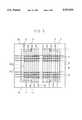
- FIG. 1is a plan view illustrating one embodiment of the liquid crystal display apparatus according to the present invention.
- FIG. 2is a cross sectional view illustrating point P and the neighborhood of the point P in a cross sectional view taken along line A--A in FIG. 1;
- FIG. 3is a plan view illustrating another embodiment of the liquid crystal display apparatus according to the present invention.
- FIG. 4is an explanatory diagram illustrating the method for repairing the disconnection defect in the liquid crystal display apparatus of another embodiment according to the present invention.
- FIG. 5is a plan view of an embodiment of a conventional liquid crystal display apparatus
- FIG. 6is a cross sectional view illustrating point P and the neighborhood of the point P in a cross sectional view taken along line B--B in FIG. 5;
- FIG. 7is a plan view of another conventional liquid crystal display apparatus for solving the problem related with the conventional liquid crystal display apparatus.
- FIG. 8is an explanatory diagram illustrating the method for repairing the disconnection defect in the conventional liquid crystal display apparatus.
- FIG. 1is a plan view illustrating an example of the liquid crystal display implementing the present invention.
- FIG. 2is a cross-sectional view illustrating point P and the neighborhood of the point P in a cross sectional view taken along line A--A in FIG. 1.
- reference numeral 1indicates a transparent insulating substrate
- 2indicates gate signal lines provided in parallel with each other and spaced at substantially equal intervals on the transparent insulating substrate such that a distance between each gate signal line and immediately adjacent gate signal line is substantially equal for gate signal line.
- Reference numeral 3indicates source signal lines provided in parallel with each other and spaced at substantially equal intervals such that a distance between each source signal line and immediately adjacent source signal line is substantially equal for each source signal line.
- the source signal linescross the gate signal lines at a right angle.
- Reference numeral 4indicates thin film transistors each of which is provided at each intersecting portions of the gate signal lines and the source signal lines.
- Reference numeral 5indicates terminals which are provided at each end portion of the gate signal lines and at each end portion of the source signal lines.
- Reference numeral 6indicates intersecting portions, and numeral 7b indicates a second insulating film formed over a neighborhood of the end portions.
- Reference numeral 8indicates a displaying section in which the thin film transistors are provided.
- Reference numeral 9indicates an auxiliary line, and numeral 10 indicates disconnection defect. Since FIG. 1 is a plan view, the insulating film is not shown therein.
- the source signal linesare grouped into some groups of the source signal lines. In each group, the source signal lines are arranged so that the group consists of a plurality of source signal lines which are adjacent to each other.
- a portion formed in the displaying sectionis referred to as a first insulating film 7a (not shown in figures), and the remaining portion formed in the outside area of the displaying section is referred to as a second insulating film 7b.
- the two insulating films 7a and 7bare sometimes referred to as an insulating film 7.
- auxiliary lines 9are arranged and provided so that the auxiliary lines 9 surround the circumference of the displaying section and so that the auxiliary lines 9 form the intersecting portions 6 as right-angled portions, the portions 6 intervening the source signal lines 3 and the second insulating film 7b.
- At least one group of source signal lines 3is arranged so that only one of ends (i.e., the end opposing a respective terminal 5) of the lines 3 intersect the outer auxiliary lines 9. Consequently, the intersecting portion with the auxiliary line 9 is not formed at the end. This is a remarkable feature of the present invention.
- a group of the source signal lines 3 provided in the central area of the displaying section 8the ends opposing the respective terminal 5 of the lines 3 intersect to the outer auxiliary lines 9.
- the inner auxiliary line 9is provided so that the ends opposing respective to each terminals 5 of the source lines 3 of a group in the neighborhood of the central area of the displaying section do not intersect and so that the source signal lines 3 are extended by the length (i.e., D or E) necessary for intersecting with the source signal lines 3 in both end portions and are terminated.
- the length of the auxiliary line 9is referred to as a surrounding length and the length D or E of the outside area of the displaying section 8 is referred to as an extended length.
- the auxiliary linesare thus provided, the source signal lines in each group have each intersecting portions of a specified auxiliary line.
- the number of the source signal lines of which end portions opposing to these terminals 5 intersect auxiliary lines 9 at a right angle or do not intersectdepends upon the number of the auxiliary lines provided in the outside area of the displaying section In FIG. 1, two auxiliary lines 9 are formed into the two grouped areas of the displaying section 8. If a large number of auxiliary lines can be provided keeping the given distance and parallel with each other, the number of group may be increased. In this case, since the number of the source signal lines in one group is fewer the parasitic capacitance of the auxiliary line may be decreased.
- auxiliary linesare grouped equally to the right side and the left side of the displaying section, and provided respectively. Then, it is sufficient that five auxiliary lines are provided.
- the number of the source signal lines in one groupis 240.
- the outermost auxiliary line 9is employed.
- the number of the intersecting portions 6is decreased to 1440, as compared with 2400 in the case of the conventional embodiment.
- the time constant of the signalis decreased to two-third of the conventional embodiment even if the capacitance of the intersecting portion is summed up. In such above-mentioned embodiment, when a disconnection defect 10 occurred and the source signal line 3 which had the defect 10 was repaired and the repaired panel was driven, there was no problem with regard to displaying characteristics.
- Conduction test of the intersecting portion 6 and driving test of the repaired panelare performed with inspection instruments before a board for a driver IC and a board for a control circuit are mounted.
- the number of the auxiliary lines assigned for a group of the source signal linesis substantially one, and the number of the source signal lines 3 of which the defects are repairable is limitted to one. Consequently, when two disconnection defects occur per one group, although the possibility is low, in the above-mentioned arrangement in which the auxiliary line 9 is assinged for one group of the source signal lines 3, the panel cannot be repaired. In order to solve the problem, it is enough that the number of the auxiliary lines is simply increased, for example the number is doubled.
- FIG. 3is a plan view illustrating another embodiment of the liquid crystal display implementing the present invention.
- reference numerals 1 to 9indicate the same portions as the numerals in FIG. 1 and FIG. 2.
- Reference numerals 3a and 3bindicate source signal lines
- numerals 10a and 10bindicate disconnection defect
- numeral 11indicates a metallic pattern film
- numerals 12a and 12bindicate intersecting portions. As shown in FIG.
- the metallic pattern film 11be provided crossing two parallel auxiliary lines 9 at a right angle to the lines 9 and on a boundary line by which a plurality of source signal lines are grouped and that an additional insulating film intervenes between the lines 9 and the metallic pattern film 11.
- the metallic pattern film 11if the film 11 is made with the same material and is made in the same layer, the second insulating film 7b can be substituted for the additional insulating film between the metallic pattern film 11 and the auxiliary line 9. Consequently, such an embodiment with the metallic pattern film 11 can be implemented without an additional process to the above-mentioned embodiment shown in FIG. 1.
- FIG. 4illustrates partially enlarged explanatory diagram taken from the FIG. 3.
- the signalsare transmitted along the source signal lines 3a and 3b as shown with an arrow in FIG. 4 by connecting electrically the metallic pattern film 11 to the auxiliary line 9 at the intersecting portions 12a and 12b shown as black spots and further by cutting the auxiliary line 9 at an appropriate position, for example the position denoted as numeral 13 by laser irradiation.
- Silicon nitridefor example, which is a typical material for an insulating film, is employed for the insulating film 7.
- the film 7may be formed, for example, with silicon oxide.
- silicon oxidesince although the relative dielectric constant of silicon nitride is approximately 7 and the relative dielectric constant of silicon oxide is approximately 4, the parasitic capacitance at the intersecting portion 6 may be decreased.
- the insulating film 7is formed with tantalum oxide, since the relative dielectric constant of the tantalum oxide is approximately 20 and is significantly larger than the relative dielectric constant of silicon oxide, also in case when the thickness of the insulating film is formed thicker, displaying characteristic of the liquid crystal display is not deteriorated. Consequently, since the thickness of the insulating film in the intersecting portion 6 may be formed thicker, an occurrence of short-circuiting defect between layers due to foreign materials (or fine particles) or so may be suppressed.
- the above-mentioned forming processcorresponds to forming in the forming process for both the first insulating film 7a and the second insulating film 7b in one process.
- the first insulating film 7a and the second insulating film 7bmay be formed individually in respective forming process.
- the second insulating film 7bmay be formed with silicon nitride and also may be formed with one of other materials, for example, silicon oxide. As described above, the parasitic capacitance at the intersecting portion 6 may be decreased.
- the liquid crystal display apparatussince the number of the intersecting portions of the auxiliary line and the source signal line may be decreased, increase of the parasitic capacitance may be suppressed. As a result, since the repair of the disconnection defect can be confirmed before the board for the driver IC and the board for the control circuit are mounted, the liquid crystal display apparatus of which the production cost is low and the production yield is enhanced.
Landscapes
- Physics & Mathematics (AREA)
- Nonlinear Science (AREA)
- Mathematical Physics (AREA)
- Chemical & Material Sciences (AREA)
- Crystallography & Structural Chemistry (AREA)
- General Physics & Mathematics (AREA)
- Optics & Photonics (AREA)
- Engineering & Computer Science (AREA)
- Microelectronics & Electronic Packaging (AREA)
- Liquid Crystal (AREA)
- Devices For Indicating Variable Information By Combining Individual Elements (AREA)
Abstract
Description
Claims (10)
Applications Claiming Priority (2)
| Application Number | Priority Date | Filing Date | Title |
|---|---|---|---|
| JP7-242983 | 1995-09-21 | ||
| JP24298395 | 1995-09-21 |
Publications (1)
| Publication Number | Publication Date |
|---|---|
| US5767929Atrue US5767929A (en) | 1998-06-16 |
Family
ID=17097158
Family Applications (1)
| Application Number | Title | Priority Date | Filing Date |
|---|---|---|---|
| US08/674,714Expired - Fee RelatedUS5767929A (en) | 1995-09-21 | 1996-07-02 | Liquid crystal display apparatus with shorting ring |
Country Status (4)
| Country | Link |
|---|---|
| US (1) | US5767929A (en) |
| KR (1) | KR100230666B1 (en) |
| CN (1) | CN1080893C (en) |
| TW (1) | TW406204B (en) |
Cited By (19)
| Publication number | Priority date | Publication date | Assignee | Title |
|---|---|---|---|---|
| US5969779A (en)* | 1995-09-06 | 1999-10-19 | Samsung Electronics Co., Ltd. | Liquid crystal display having a repair line |
| US6014191A (en)* | 1996-07-16 | 2000-01-11 | Samsung Electronics Co., Ltd. | Liquid crystal display having repair lines that cross data lines twice and cross gate lines in the active area and related repairing methods |
| US6025891A (en)* | 1996-11-29 | 2000-02-15 | Lg Electronics Inc. | Liquid crystal display device |
| US6088073A (en)* | 1997-04-14 | 2000-07-11 | Casio Computer Co., Ltd. | Display device with destaticizing elements and an electrostatic pulse delaying element connected to each of the destaticizing elements |
| US6111621A (en)* | 1997-04-03 | 2000-08-29 | Samsung Electronics Co., Ltd. | Flat panel display devices having improved signal line repair capability |
| US6128051A (en)* | 1997-09-12 | 2000-10-03 | Lg Electronics Inc. | Method for forming and apparatus including a liquid crystal display having shorting bar connector |
| US6184948B1 (en)* | 1997-02-11 | 2001-02-06 | Lg Electronics Inc. | Liquid crystal display device having a plurality of error detecting shorting bars and a method of manufacturing the same |
| US6288765B1 (en)* | 1998-10-01 | 2001-09-11 | Sharp Kabushiki Kaisha | Liquid crystal display device having improved thickness uniformity |
| US6333771B1 (en)* | 1997-12-26 | 2001-12-25 | Sharp Kabushiki Kaisha | Liquid crystal display device capable of reducing the influence of parasitic capacities |
| US20020085169A1 (en)* | 2000-12-30 | 2002-07-04 | Choi Gyo Un | Liquid crystal display for testing defects of wiring in panel |
| US6429908B1 (en)* | 1997-09-30 | 2002-08-06 | Lg Philips Lcd Co., Ltd. | Method for manufacturing a gate of thin film transistor in a liquid crystal display device |
| US6570630B2 (en)* | 1997-03-26 | 2003-05-27 | Sharp Kabushiki Kaisha | Display panel |
| US20060103410A1 (en)* | 2004-11-16 | 2006-05-18 | Samsung Electronics Co., Ltd. | Panel and test method for display device |
| US20090057682A1 (en)* | 2006-02-24 | 2009-03-05 | Sharp Kabushiki Kaisha | Active matrix substrate, display device, television receiver, manufacturing method of active matrix substrate, forming method of gate insulating film |
| US20090261338A1 (en)* | 2006-02-24 | 2009-10-22 | Sharp Kabushiki Kaisha | Active matrix substrate, display device, and television receiver |
| US20090262274A1 (en)* | 2004-12-14 | 2009-10-22 | Sharp Kabushiki Kaisha | Liquid crystal display and a defect correcting method for the same |
| US7755712B2 (en) | 2006-09-11 | 2010-07-13 | Au Optronics Corp. | Array substrate, and method for repairing thereof, and display panel and display apparatus comprising the same |
| CN105607360A (en)* | 2015-12-25 | 2016-05-25 | 上海中航光电子有限公司 | Display panel and display device |
| US10180745B2 (en) | 2015-12-25 | 2019-01-15 | Shanghai Avic Optoelectronics Co., Ltd. | Display panel and display device with narrow bezel |
Families Citing this family (7)
| Publication number | Priority date | Publication date | Assignee | Title |
|---|---|---|---|---|
| CN100555027C (en)* | 2003-06-19 | 2009-10-28 | 日本电信电话株式会社 | Optic modulating device |
| CN100498491C (en)* | 2005-10-26 | 2009-06-10 | 中华映管股份有限公司 | Liquid crystal display and thin film transistor array substrate thereof |
| CN100514130C (en)* | 2006-02-06 | 2009-07-15 | 中华映管股份有限公司 | Liquid crystal display device with a light guide plate |
| TWI447499B (en)* | 2009-10-27 | 2014-08-01 | Lg Display Co Ltd | Array substrate of liquid crystal display device, liquid crystal display device and method of manufacturing same |
| CN103207487B (en)* | 2013-03-26 | 2015-08-05 | 北京京东方光电科技有限公司 | The method for maintaining of array base palte, display device and array base palte |
| CN103365015B (en)* | 2013-07-11 | 2016-01-06 | 北京京东方光电科技有限公司 | A kind of array base palte and liquid crystal display |
| CN108139640A (en)* | 2015-10-06 | 2018-06-08 | 堺显示器制品株式会社 | Display device |
Citations (11)
| Publication number | Priority date | Publication date | Assignee | Title |
|---|---|---|---|---|
| JPH0385525A (en)* | 1989-08-29 | 1991-04-10 | Sharp Corp | Matrix type display device |
| JPH052175A (en)* | 1991-06-25 | 1993-01-08 | Sanyo Electric Co Ltd | Liquid crystal display device |
| JPH052176A (en)* | 1991-06-25 | 1993-01-08 | Sanyo Electric Co Ltd | Liquid crystal display device |
| JPH052180A (en)* | 1991-06-25 | 1993-01-08 | Sanyo Electric Co Ltd | Liquid crystal display device |
| US5233448A (en)* | 1992-05-04 | 1993-08-03 | Industrial Technology Research Institute | Method of manufacturing a liquid crystal display panel including photoconductive electrostatic protection |
| JPH05203986A (en)* | 1992-01-27 | 1993-08-13 | Nec Corp | Liquid crystal display device |
| US5313319A (en)* | 1992-06-17 | 1994-05-17 | General Electric Company | Active array static protection devices |
| US5373377A (en)* | 1992-02-21 | 1994-12-13 | Kabushiki Kaisha Toshiba | Liquid crystal device with shorting ring and transistors for electrostatic discharge protection |
| US5504348A (en)* | 1992-08-13 | 1996-04-02 | Casio Computer Co., Ltd. | Thin-film transistor array and liquid crystal display device using the thin-film transistor array |
| US5596342A (en)* | 1993-11-10 | 1997-01-21 | International Business Machines Corporation | Display device having separate short circuit wires for data and gate lines for protection against static discharges |
| US5671026A (en)* | 1994-03-02 | 1997-09-23 | Sharp Kabushiki Kaisha | Liquid crystal display device with TFT ESD protective devices between I/O terminals or with a short circuited alignment film |
- 1996
- 1996-07-02USUS08/674,714patent/US5767929A/ennot_activeExpired - Fee Related
- 1996-07-02TWTW085107981Apatent/TW406204B/ennot_activeIP Right Cessation
- 1996-07-13KRKR1019960028786Apatent/KR100230666B1/ennot_activeExpired - Fee Related
- 1996-08-20CNCN96111150Apatent/CN1080893C/ennot_activeExpired - Fee Related
Patent Citations (11)
| Publication number | Priority date | Publication date | Assignee | Title |
|---|---|---|---|---|
| JPH0385525A (en)* | 1989-08-29 | 1991-04-10 | Sharp Corp | Matrix type display device |
| JPH052175A (en)* | 1991-06-25 | 1993-01-08 | Sanyo Electric Co Ltd | Liquid crystal display device |
| JPH052176A (en)* | 1991-06-25 | 1993-01-08 | Sanyo Electric Co Ltd | Liquid crystal display device |
| JPH052180A (en)* | 1991-06-25 | 1993-01-08 | Sanyo Electric Co Ltd | Liquid crystal display device |
| JPH05203986A (en)* | 1992-01-27 | 1993-08-13 | Nec Corp | Liquid crystal display device |
| US5373377A (en)* | 1992-02-21 | 1994-12-13 | Kabushiki Kaisha Toshiba | Liquid crystal device with shorting ring and transistors for electrostatic discharge protection |
| US5233448A (en)* | 1992-05-04 | 1993-08-03 | Industrial Technology Research Institute | Method of manufacturing a liquid crystal display panel including photoconductive electrostatic protection |
| US5313319A (en)* | 1992-06-17 | 1994-05-17 | General Electric Company | Active array static protection devices |
| US5504348A (en)* | 1992-08-13 | 1996-04-02 | Casio Computer Co., Ltd. | Thin-film transistor array and liquid crystal display device using the thin-film transistor array |
| US5596342A (en)* | 1993-11-10 | 1997-01-21 | International Business Machines Corporation | Display device having separate short circuit wires for data and gate lines for protection against static discharges |
| US5671026A (en)* | 1994-03-02 | 1997-09-23 | Sharp Kabushiki Kaisha | Liquid crystal display device with TFT ESD protective devices between I/O terminals or with a short circuited alignment film |
Cited By (37)
| Publication number | Priority date | Publication date | Assignee | Title |
|---|---|---|---|---|
| US5969779A (en)* | 1995-09-06 | 1999-10-19 | Samsung Electronics Co., Ltd. | Liquid crystal display having a repair line |
| US7535521B2 (en) | 1996-07-16 | 2009-05-19 | Samsung Electronics Co., Ltd. | LCD having repair lines wherein first and second signal lines include means for receiving the same gate signal thereon are formed on a TFT insulating substrate |
| US6014191A (en)* | 1996-07-16 | 2000-01-11 | Samsung Electronics Co., Ltd. | Liquid crystal display having repair lines that cross data lines twice and cross gate lines in the active area and related repairing methods |
| US20040012727A1 (en)* | 1996-07-16 | 2004-01-22 | Dong-Gyu Kim | Liquid crystal display having repair lines and methods of repairing the same |
| US6618101B1 (en)* | 1996-07-16 | 2003-09-09 | Samsung Electronics Co., Ltd. | Liquid crystal display having repair lines and methods of repairing the same |
| US6100949A (en)* | 1996-11-29 | 2000-08-08 | Lg Electronics Inc. | Liquid crystal display device having electrostatic discharge protection |
| US6025891A (en)* | 1996-11-29 | 2000-02-15 | Lg Electronics Inc. | Liquid crystal display device |
| US6184948B1 (en)* | 1997-02-11 | 2001-02-06 | Lg Electronics Inc. | Liquid crystal display device having a plurality of error detecting shorting bars and a method of manufacturing the same |
| US6765630B2 (en) | 1997-03-26 | 2004-07-20 | Sharp Kabushiki Kaisha | Display panel |
| US6570630B2 (en)* | 1997-03-26 | 2003-05-27 | Sharp Kabushiki Kaisha | Display panel |
| US20030112402A1 (en)* | 1997-03-26 | 2003-06-19 | Sharp Kabushiki Kaisha | Display panel |
| US20030117537A1 (en)* | 1997-03-26 | 2003-06-26 | Sharp Kabushiki Kaisha | Display panel |
| US6111621A (en)* | 1997-04-03 | 2000-08-29 | Samsung Electronics Co., Ltd. | Flat panel display devices having improved signal line repair capability |
| US6088073A (en)* | 1997-04-14 | 2000-07-11 | Casio Computer Co., Ltd. | Display device with destaticizing elements and an electrostatic pulse delaying element connected to each of the destaticizing elements |
| US6128051A (en)* | 1997-09-12 | 2000-10-03 | Lg Electronics Inc. | Method for forming and apparatus including a liquid crystal display having shorting bar connector |
| US6429908B1 (en)* | 1997-09-30 | 2002-08-06 | Lg Philips Lcd Co., Ltd. | Method for manufacturing a gate of thin film transistor in a liquid crystal display device |
| US6333771B1 (en)* | 1997-12-26 | 2001-12-25 | Sharp Kabushiki Kaisha | Liquid crystal display device capable of reducing the influence of parasitic capacities |
| US6608655B2 (en) | 1997-12-26 | 2003-08-19 | Sharp Kabushiki Kaisha | Liquid crystal display device including identical shape dummy wire surrounding each pixel and capable of reducing the influence of parasitic capacities |
| US6288765B1 (en)* | 1998-10-01 | 2001-09-11 | Sharp Kabushiki Kaisha | Liquid crystal display device having improved thickness uniformity |
| US20020085169A1 (en)* | 2000-12-30 | 2002-07-04 | Choi Gyo Un | Liquid crystal display for testing defects of wiring in panel |
| US6999153B2 (en)* | 2000-12-30 | 2006-02-14 | Boe-Hydis Technology Co., Ltd. | Liquid crystal display for testing defects of wiring in panel |
| US20060103410A1 (en)* | 2004-11-16 | 2006-05-18 | Samsung Electronics Co., Ltd. | Panel and test method for display device |
| US7288955B2 (en)* | 2004-11-16 | 2007-10-30 | Samsung Electronics Co., Ltd. | Panel and test method for display device |
| US20080007287A1 (en)* | 2004-11-16 | 2008-01-10 | Sang-Jin Jeon | Panel and test method for display device |
| US7504848B2 (en)* | 2004-11-16 | 2009-03-17 | Samsung Electronics, Co., Ltd. | Panel and test method for display device |
| US20090262274A1 (en)* | 2004-12-14 | 2009-10-22 | Sharp Kabushiki Kaisha | Liquid crystal display and a defect correcting method for the same |
| US7777825B2 (en) | 2004-12-14 | 2010-08-17 | Sharp Kabushiki Kaisha | Liquid crystal display and a defect correcting method for the same |
| US20090261338A1 (en)* | 2006-02-24 | 2009-10-22 | Sharp Kabushiki Kaisha | Active matrix substrate, display device, and television receiver |
| US20090057682A1 (en)* | 2006-02-24 | 2009-03-05 | Sharp Kabushiki Kaisha | Active matrix substrate, display device, television receiver, manufacturing method of active matrix substrate, forming method of gate insulating film |
| US7868960B2 (en) | 2006-02-24 | 2011-01-11 | Sharp Kabushiki Kaisha | Active matrix substrate, display device, and television receiver |
| US8168980B2 (en) | 2006-02-24 | 2012-05-01 | Sharp Kabushiki Kaisha | Active matrix substrate, display device, television receiver, manufacturing method of active matrix substrate, forming method of gate insulating film |
| US7755712B2 (en) | 2006-09-11 | 2010-07-13 | Au Optronics Corp. | Array substrate, and method for repairing thereof, and display panel and display apparatus comprising the same |
| US20100193222A1 (en)* | 2006-09-11 | 2010-08-05 | Au Optronics Corp. | Array Substrate, and Method for Repairing Thereof, and Display Panel and Display Apparatus Comprising the Same |
| US8077270B2 (en) | 2006-09-11 | 2011-12-13 | Au Optronics Corp. | Array substrate, and method for repairing thereof, and display panel and display apparatus comprising the same |
| CN105607360A (en)* | 2015-12-25 | 2016-05-25 | 上海中航光电子有限公司 | Display panel and display device |
| US10180745B2 (en) | 2015-12-25 | 2019-01-15 | Shanghai Avic Optoelectronics Co., Ltd. | Display panel and display device with narrow bezel |
| CN105607360B (en)* | 2015-12-25 | 2019-07-05 | 上海中航光电子有限公司 | A kind of display panel and display device |
Also Published As
| Publication number | Publication date |
|---|---|
| CN1166614A (en) | 1997-12-03 |
| CN1080893C (en) | 2002-03-13 |
| KR970016708A (en) | 1997-04-28 |
| KR100230666B1 (en) | 1999-11-15 |
| TW406204B (en) | 2000-09-21 |
Similar Documents
| Publication | Publication Date | Title |
|---|---|---|
| US5767929A (en) | Liquid crystal display apparatus with shorting ring | |
| US5668032A (en) | Active matrix ESD protection and testing scheme | |
| US5019002A (en) | Method of manufacturing flat panel backplanes including electrostatic discharge prevention and displays made thereby | |
| US5852480A (en) | LCD panel having a plurality of shunt buses | |
| US6111558A (en) | Liquid crystal displays including closed loop repair lines and methods of repairing same | |
| KR100355966B1 (en) | Display panel | |
| US20070284578A1 (en) | Array substrate for liquid crystal display and method of testing | |
| EP1008177B1 (en) | Improved active matrix esd protection and testing scheme | |
| US6613650B1 (en) | Active matrix ESD protection and testing scheme | |
| US6380992B1 (en) | Liquid crystal display device having a defective pad repair structure and method for making the same | |
| US5608245A (en) | Array on substrate with repair line crossing lines in the array | |
| US20080304003A1 (en) | Repairing method of a thin film transistor array substrate | |
| US7777824B2 (en) | Liquid crystal display device and repair structure with electrode overlapped to data line | |
| EP0842455A1 (en) | Improved tft, method of making and matrix displays incorporating the tft | |
| JP3251474B2 (en) | Active matrix substrate | |
| JP3066569B2 (en) | Liquid crystal display | |
| US7053977B2 (en) | Laser repair structure of liquid crystal display device and method thereof | |
| US5731854A (en) | Method of effectively dispersing static electricity in LCD production by placing a short line in the end region of one substrate which extends beyond the other substrate | |
| KR20000065730A (en) | TFT array substrate of LCD device and method for testing the same | |
| JPH11305260A (en) | Active matrix type liquid crystal display device and pixel defect repair method | |
| JPH05203986A (en) | Liquid crystal display device | |
| KR100695614B1 (en) | One pixel repair method using laser chemical vapor deposition equipment and substrate of repaired liquid crystal display device using the same | |
| JPH08271930A (en) | Method for manufacturing thin film transistor | |
| JPH0355985B2 (en) | ||
| JPH0394223A (en) | Manufacture of active matrix display device |
Legal Events
| Date | Code | Title | Description |
|---|---|---|---|
| AS | Assignment | Owner name:ADVANCED DISPLAY CO., LTD, JAPAN Free format text:ASSIGNMENT OF ASSIGNORS INTEREST;ASSIGNORS:YACHI, SHIGERU;NAKAGAWA, NAOKI;KIKUDA, SHIGERU;REEL/FRAME:008095/0117 Effective date:19960514 | |
| FEPP | Fee payment procedure | Free format text:PAYOR NUMBER ASSIGNED (ORIGINAL EVENT CODE: ASPN); ENTITY STATUS OF PATENT OWNER: LARGE ENTITY | |
| AS | Assignment | Owner name:ADVANCED DISPLAY INC., JAPAN Free format text:ASSIGNMENT OF ASSIGNORS INTEREST;ASSIGNORS:YACHI, SHIGERU;NAKAGAWA, NAOKI;KIKUDA, SHIGERU;REEL/FRAME:008931/0114 Effective date:19971215 | |
| FPAY | Fee payment | Year of fee payment:4 | |
| FPAY | Fee payment | Year of fee payment:8 | |
| AS | Assignment | Owner name:MITSUBISHI ELECTRIC CORPORATION, JAPAN Free format text:ASSIGNMENT OF ASSIGNORS INTEREST;ASSIGNOR:ADVANCED DISPLAY INC.;REEL/FRAME:020270/0075 Effective date:20071128 | |
| REMI | Maintenance fee reminder mailed | ||
| LAPS | Lapse for failure to pay maintenance fees | ||
| STCH | Information on status: patent discontinuation | Free format text:PATENT EXPIRED DUE TO NONPAYMENT OF MAINTENANCE FEES UNDER 37 CFR 1.362 | |
| FP | Lapsed due to failure to pay maintenance fee | Effective date:20100616 |