US5767643A - Commutation delay generator for a multiphase brushless DC motor - Google Patents
Commutation delay generator for a multiphase brushless DC motorDownload PDFInfo
- Publication number
- US5767643A US5767643AUS08/595,812US59581296AUS5767643AUS 5767643 AUS5767643 AUS 5767643AUS 59581296 AUS59581296 AUS 59581296AUS 5767643 AUS5767643 AUS 5767643A
- Authority
- US
- United States
- Prior art keywords
- delay
- commutation
- node
- circuit
- current
- Prior art date
- Legal status (The legal status is an assumption and is not a legal conclusion. Google has not performed a legal analysis and makes no representation as to the accuracy of the status listed.)
- Expired - Lifetime
Links
Images


Classifications
- H—ELECTRICITY
- H02—GENERATION; CONVERSION OR DISTRIBUTION OF ELECTRIC POWER
- H02P—CONTROL OR REGULATION OF ELECTRIC MOTORS, ELECTRIC GENERATORS OR DYNAMO-ELECTRIC CONVERTERS; CONTROLLING TRANSFORMERS, REACTORS OR CHOKE COILS
- H02P6/00—Arrangements for controlling synchronous motors or other dynamo-electric motors using electronic commutation dependent on the rotor position; Electronic commutators therefor
- H02P6/14—Electronic commutators
- H02P6/15—Controlling commutation time
Definitions
- This inventionrelates generally to commutation circuits for electric motors.
- Hard disk drive systemsare a predominant mechanism for providing large volumes of low-cost, computer-accessible memory.
- a typical hard driveincludes a spin motor for rotating one or more magnetic storage disks during data read and write operations.
- An electronic control and driving circuitis coupled between the spin motor and a host microprocessor interface to provide drive signals to power the motor windings.
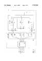
- FIG. 1is a schematic diagram of conventional motor and drive circuitry 7, which includes a portion of a three-phase brushless spin motor 10 connected to a conventional commutation sequencer 18 via a motor driver 20.
- spin motor 10is assumed to include three sets of phase windings, each of which is selectively driven at a predetermined phase.
- the three sets of windingsare represented by phase windings 12, 14, and 16, which are arranged around a rotor shaft (not shown) and have a common connection at a center tap 11.
- sequencer 18 and a motor driver 20collectively operate to selectively drive pairs of phase windings 12, 14, and 16 to induce rotation of the rotor shaft of motor 10.
- Diodes D 1 -D 6protect motor and drive circuitry 7 from extreme voltages on nodes A, B, and C that would otherwise result due to the inductances of windings 12, 14, and 16.
- traces 1, 2, and 3illustrate the motor torque generated when a constant current flows through selected pairs of phase windings 12, 14, and 16.
- Trace 1shows the motor torque curve with respect to electrical degrees when transistors 20a and 20f are turned on (20b through 20e turned off), resulting in current flow through phase-A winding 12 and phase-C winding 16.
- trace 2shows the motor torque curve on the common horizontal axis when transistors 20a and 20d are turned on, resulting in current flow through phase-A winding 12 and phase-B winding 14.
- trace 3shows the motor torque curve when transistors 20d and 20e are turned on, resulting in current flow through phase-C winding 16 and phase-B winding 14.
- the maximum torque pointsoccur 60 electrical degrees apart. For an eight-pole motor, 60 electrical degrees correspond equivalently to 15° of mechanical rotation of the rotor shaft.
- the motor torqueshould be either continuously positive or continuously negative.
- a continuously positive motor torquefor example, can be provided by designing and controlling sequencer 18 and motor driver 20 to transfer current to selected pairs of windings in a predetermined and precisely timed sequence so that the overall torque curve of the motor is defined along the maximum segments connecting points a1 through a7 of FIG. 2A. The act of transferring current from one pair of windings to the next is conventionally called "commutation.”
- the overall torque curve defined by the curves connecting points a1 through a7results in maximum torque with the least ripple, and thus is considered the result of optimal commutation timing.
- the predetermined sequence required for turning on the transistors 20a through 20f, as controlled by sequencer 18,is as follows:
- Transistors 20a and 20fare on so that current flows from node A through windings 12 and 16 to node C, generating torque segment a1 to a2;
- Transistors 20a and 20dare on so that current flows from node A through windings 12 and 14 to node B, generating torque segment a2 to a3;
- Transistors 20d and 20eare on so that current flows from node C through windings 16 and 14 to terminal B, generating torque segment a3 to a4;
- Transistors 20b and 20eare on so that current flows from node C through windings 16 and 12 to node A, generating torque segment a4 to a5;
- Transistors 20b and 20care on so that current flows from node B through windings 14 and 12 to node A, generating torque segment a5 to a6;
- Transistors 20c and 20fare on so that current flows from node B through windings 14 and 16 to node C, generating torque segment a6 to a7.
- BEMFback electromotive force
- the motoris commutated at 30 electrical degrees before and after the maximum torque points. These ideal motor commutation times are shown both in FIG. 2C and in FIG. 3A as the signal "FCOM,” which conventionally stands for “frequency of commutation.” In the vernacular of motor engineers, the individual pulses of the FCOM signal may be referred to as "FCOM pulses.”
- Analog comparatorsare connected across each phase winding 12, 14, and 16 of the motor to determine when each of the BEMF signals is greater than zero.
- the output signals generated by these comparatorsare shown in FIGS. 3B through 3D.
- the comparator signals of FIGS. 3B through 3Dare logically decoded, using conventional means, to generate the tachometer signal shown in FIG. 3E. It is noted that the optimal motor commutation times are shown to occur at the midpoint of each high and low state of the tachometer signal as represented at points X and Y, respectively, of FIG. 3E.
- each high and low state of the tachometer signalare determined in accordance with the circuits of FIGS. 4A and 4B.
- the voltage waveforms generated across capacitors 22 and 28 of the circuitsare shown in FIGS. 3F and 3G, respectively.
- capacitor 22is charged with a conventional constant-current source 24 during the high period of the tachometer signal and is then discharged at twice the rate with a second conventional constant-current sink 26 after the tachometer signal changes states.
- the capacitor 22reaches its lowest level at point Y, which is the desired time to commutate the motor.
- Capacitor 22is combined with conventional sensing and triggering circuitry (not shown) connected to the sequencer 18 to thereby commutate the motor driver 20 to the next phase.
- Capacitor 28 of FIG. 4Bis provided to determine the commutation points labeled X. This is accomplished by charging capacitor 28 with a constant-current source 27 during the time at which capacitor 22 is being discharged, and then holding the voltage charged until the tachometer signal changes to a high state. At this time, capacitor 28 is discharged with a constant-current sink 29 that provides a current equal in magnitude but opposite in polarity as compared to the output current of constant-current source 27. When the capacitor 28 reaches its minimum voltage level, conventional sensing and triggering circuitry (not shown) senses the minimum voltage condition and issues an FCOM pulse to sequencer 18, thereby causing sequencer 18 to select the next phase state (i.e., the next pair of windings).
- the above-described BEMF technique for determining commutation timingworks well in that when the spin motor is first starting up the commutation points are not fixed in time. If the values of capacitors 22 and 28 are chosen correctly, the method can be used to commutate the motor even during the initial spin-up of the motor, during which time the frequency of the tachometer signal varies.
- the upper charge levels of capacitors 22 and 28are not critical; if the period is longer, the capacitors 22 and 28 simply charge to a higher level.
- the tachometer signalchanges states due to a zero-crossing of the BEMF signal, the respective capacitor 22 or 28 will be discharged. When the lowest voltage level or some other predetermined voltage threshold level is reached, the sensing and triggering electronics sequences the motor to the next commutation state.
- the techniqueis seemingly ideal, it is not without practical problems.
- the tach signal of FIG. 3Eis not exactly symmetrical due to e.g. errors in the spacing between magnetic poles of windings or random noise that cause erroneous determinations of BEMF zero-cross times.
- the timing of a given FCOM pulseis a function of the time period between two prior BEMF zero-cross times, any such variation in the measured spacing between preceding zero-crossing times may cause the motor to commutate to the next phase at the wrong time.
- Such erroneous commutation timingresults in repetitive instants of sub-optimum torque, which in turn result in an undesirable phenomenon commonly known as "jitter.”
- the present inventionaddresses the aforementioned need by providing an inventive commutation control circuit that is insensitive to short-term variations in BEMF zero-cross timing.
- the commutation control circuitincludes a frequency-to-current converter that receives the periodic series of commutation signals as input and outputs a delay current of a magnitude that is inversely proportional to the average period of the series of commutation signals (i.e., the average FCOM period). This proportional current is used to charge a delay capacitance of known value to provide a selected voltage change across the delay capacitance.
- the charging time of the capacitanceis also proportional to the average commutation period. For example, if the delay current were to double, the charge time of the delay capacitance would decrease by a factor of two. Similarly, if the delay current were to decrease by a factor of two, the charge time of the delay capacitance would double.
- the commutation delay generatoralso includes a back-EMF sensor that senses the back EMF induced in an unpowered winding of the motor.
- the level of the back EMFprovides an indication of the position of the rotor.
- the delay circuitbegins to charge the delay capacitance with the delay current.
- the delay circuitissues an FCOM pulse to commutate the motor.
- the delay capacitanceis alternately charged and discharged a number of times to provide an increased total voltage change without requiring an increased supply voltage.
- This embodimentallows for the use of a relatively small capacitor to provide the delay capacitance.
- FIG. 1is a schematic diagram of conventional motor and select circuitry 7;
- FIG. 2Ais a set of traces illustrating motor torque with respect to motor electrical degrees
- FIG. 2Bis a set of traces illustrating the BEMF signals generated in each phase winding of a spin motor with respect to motor electrical degrees;
- FIGS. 2C and 3Aare timing diagrams illustrating the ideal commutation times and active phase windings with respect to motor electrical degrees
- FIGS. 3B through 3Dare a set of traces illustrating output signals from BEMF signal comparators
- FIG. 3Eis a trace of a tachometer signal
- FIGS. 3F and 3Gare traces illustrating the voltage levels across a set of capacitors
- FIGS. 4A and 4Bare schematic diagrams of conventional circuits for determining optimal commutation times
- FIG. 5is a block diagram of a commutation control circuit coupled to a conventional spin motor
- FIG. 6is a schematic diagram of the commutation control circuit of FIG. 5;
- FIG. 7is an amplifier 72 in accordance with an embodiment of the invention.
- FIG. 8is a schematic diagram of a counter circuit 78 in accordance with an embodiment of the present invention.
- FIG. 9is a state diagram of the one-bit up/down counter 150 of FIG. 8;
- FIG. 10is a state diagram of state machine 76 of FIG. 6;
- FIG. 11is a waveform diagram describing the function of delay circuit 70 of FIG. 6.
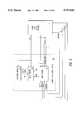
- FIG. 5is a block diagram of a commutation control circuit 50 in accordance with the present invention coupled to the conventional motor and select circuitry 7 of FIG. 1.
- Control circuit 50includes a delay circuit 70 that provides a substantially periodic series of FCOM pulses to motor and select circuitry 7 and to an averaging circuit 80.
- the FCOM pulsescause motor and select circuitry 7 to commutate from one phase to the next in the manner explained above with respect to the conventional motor and select circuitry 7 of FIG. 1.
- Averaging circuit 80receives the FCOM pulses and outputs a delay signal on line 84 to delay circuit 70.
- the delay signalis a current level of a magnitude proportional to the frequency (and therefore inversely proportional to the period) of the incoming series of FCOM pulses: the higher the commutation frequency, the higher the magnitude of the current level of the delay signal.
- BEMF sensor 90Conventional logic from motor and select circuitry 7 causes BEMF sensor 90 to select the center tap and the node of the unpowered winding (i.e., A, B, or C) so that the BEMF voltage developed across the unpowered winding is present across nodes POS and NEG.
- An input signal from sequencer 18 to terminal REVERSEensures that center tap 11 and the node of the unpowered winding are selected such that the voltage on node POS is moving in a generally positive direction relative to the voltage on node NEG.
- delay circuit 70detects a "zero cross" (i.e., when the BEMF voltage across the unpowered winding is zero) when the voltage on node POS is equal to the voltage on node NEG. Delay circuit 70 then uses the timing of the zero cross and the current level of the delay signal on line 84 to establish the appropriate timing for a subsequent FCOM pulse.
- FIG. 6is a schematic diagram of commutation control circuit 50 of FIG. 5, including averaging circuit 80, BEMF sensor 90, and delay circuit 70.
- BEMF sensor 90receives a number of input signals from motor and select circuitry 7.
- Nodes A, B, and Care electrically the same nodes as nodes A, B, and C, respectively, of FIG. 1.
- the voltage levels on nodes A, B, and Cwhen measured with respect to the voltage level on center tap 11, provide an indication of zero-cross timing.
- a resistor network 99includes four resistors that combine with capacitors 96 and 98 to create a pair of low-pass filters for the BEMF of the unpowered windings.
- the resistors of resistor network 99are typically 200 K ⁇ each, while capacitors 96 and 98 are typically 20 pF each.
- delay circuit 70senses the BEMF voltage across nodes POS and NEG to determine the timing of a zero cross. Then, delay circuit 70, using the zero cross as a timing reference, waits for a delay period T DLY equal to approximately 30 electrical degrees (i.e., approximately T FCOM /2) and outputs an FCOM pulse to motor and select circuitry 7, averaging circuit 80, and sequencer 18.
- Averaging circuit 80includes a frequency-to-current converter 82 that outputs a delay current I delay on line 84.
- the magnitude of current I delayis inversely proportional to the average period of the FCOM signal from delay circuit 70. Stated mathematically, ##EQU1## where T FCOM is the average period of e.g. one hundred FCOM pulses and ⁇ is the gain factor of frequency-to-current converter 80. Typical values for ⁇ and T FCOM are 3.47 nC and 347 ⁇ s, respectively, resulting in a delay current I delay of approximately 10 ⁇ A.
- Averaging circuit 80may be any conventional frequency-to-current converter that is configured to provide an output current proportional to the average commutation period T FCOM of the commutation signal on terminal FCOM. Because of inherent spacing errors between motor stators, it is recommended that the number of FCOM periods averaged be equal to at least the number of FCOM pulses for a single mechanical rotation, which is e.g. 24 in a eight-pole motor. The upper limit of the number of FCOM periods averaged is quite high, (e.g., one thousand), for the average FCOM period T FCOM is very small compared to the acceleration time constant of a typical motor. If the number is too high, the commutation timing will be slow to respond to changes in motor speed.
- the delay period T DLYwill be greater than T FCOM /2, causing a phase delay on the commutation. Conversely, if the factor C DLY .increment.V DLY / ⁇ is less than one half, the result will be a phase advance on the commutation.
- Delay circuit 70includes a current-controlled transconductance amplifier 72 and a delay capacitance C DLY .
- Amplifier 72receives the BEMF signal POS-NEG (i.e., the voltage difference between nodes POS and NEG) and the delay current I DLY on line 84.
- POS-NEGthe BEMF signal
- I DLYthe delay current I DLY on line 84.
- amplifier 72outputs a delay current on node V DLY that is equal in magnitude to that of the delay current I delay on line 84.
- averaging circuit 80is configured to provide some minimum level of delay current when the commutation signal on terminal FCOM has a frequency of between e.g. zero and 150 Hz. This minimum delay current develops FCOM pulses of a predetermined frequency when the motor is first started up until the commutation frequency reaches a level sufficient to develop a delay current I delay greater than the offset current. Once delay current I delay is greater than the offset current, averaging circuit 80 gains control of delay period T dly so that the delay period T DLY will behave in accordance with equation (1).
- averaging circuit 80is a frequency-to-current converter with an offset current of approximately 500 nA, and is of the type described in the above-referenced application entitled "Frequency-To-Current Converter".
- the value (and therefore physical size) of delay capacitance C DLYis minimized to allow for easier, more economical integration of the capacitance.
- the method and circuitry used to minimize capacitance C DLYis described below in connection with FIGS. 6 through 11.
- the time constant ⁇ C of capacitance Cis proportional to the product of the change in voltage .increment.V and the capacitance C divided by the charging current I C .
- This relationshipmay be expressed mathematically as: ##EQU4## According to equation (4), for a given time constant ⁇ C the necessary value of the capacitance C (and thus the physical area required to integrate such a capacitance) may be minimized by either increasing .increment.V or decreasing the current I C .
- a 16-volt .increment.V on node V DLYis folded into e.g. four segments, two decreasing and two increasing. That is, instead of charging capacitance C DLY from e.g. one to 17 volts to obtain a .increment.V of 16 volts, capacitance C DLY is charged and discharged between one and five volts four times (i.e., four 4-volt changes), for a total .increment.V of 16 volts. In this way, the necessary value of delay capacitance C DLY is decreased by a factor of four. This decrease in capacitance translates into a similar decrease in physical size that advantageously allows delay capacitance C DLY to be more readily integrated.
- the commutation delay period T DLYmay be adjusted by changing the reference voltage on terminal V DAC , and therefore the voltage range .increment.V of node V DLY , using a conventional 6-bit digital-to-analog converter 79.
- adjustable or fixed voltage referencesmay also be used.
- embodiments that include adjustable phase delayadvantageously allow users to optimize the delay period T DLY for particular applications.
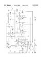
- FIG. 7is a schematic diagram of transconductance amplifier 72 coupled to delay capacitance C DLY and voltage clamp 73.
- the purpose of amplifier 72is to charge and discharge delay capacitance C DLY at a rate established by the delay current I delay .
- a zero crossis detected when the voltage on node POS "crosses" the voltage on node NEG, and that an FCOM pulse should be developed after a delay period T DLY equal to one-half of the average FCOM period T FCOM , or T FCOM /2.
- the current I delayis inversely proportional to the average FCOM period T FCOM , and is therefore also inversely proportional to a delay of T FCOM /2. Because of this proportionality, the delay period T DLY can be established by charging and discharging capacitance C DLY a predetermined number of times using the delay current I delay .
- Transconductance amplifier 72includes input transistors 106A and 106B, which receive inputs on lines POS and NEG from BEMF sensor 90. Transistors 106A and 106B are level-shift transistors that are biased by current sources 107A and 107B, respectively. Transconductance amplifier 72 also includes a POS-NEG lockout circuit 100 that causes amplifier 72 to ignore the signals on terminals POS and NEG when counter circuit 78 outputs a logic one on line LOCK. The purpose for the lock signal is described below in connection with FIGS. 8 and 9. For the present, assume that the lock signal on line LOCK is a logic zero, in which case transistors 102B and 102C are off and POS-NEG lockout circuit 100 is therefore deactivated.
- delay current I delayis mirrored first by transistors 103A and 103B then by transistors 104A and 104B to provide a current substantially equal to the delay current I delay through either transistors 108A and 110A or transistors 108B and 112A, the current path depending on the relative signal levels on terminals POS and NEG.
- the current equal to the delay current I delaywill pass through transistors 108B and 112A, and will consequently be mirrored by transistor 112B (because the voltage on line XUP is a logic zero, the output of AND gate 134 will be a logic zero; thus, transistor 116B, and therefore transistor 112C, cannot conduct).
- the current through transistor 112Bwill be mirrored by transistors 120A and 120B so that delay capacitance C DLY will be charged by a current substantially equal to the delay current I delay ; consequently, the voltage on node V DLY will increase.
- Amplifier 72exhibits the opposite behavior when the signal on line UP is a logic zero, indicating that delay capacitance C DLY is to be discharged by a current substantially equal to the delay current I delay .
- a voltage on node POS that is more positive than that on node NEGwill cause delay capacitance C DLY to discharge at a rate determined by a discharge current substantially equal to the delay current I delay .
- a voltage on node POS that is more negative than that on node NEGwill cause delay capacitance C DLY to charge at a rate determined by a current substantially equal to delay current I delay . This behavior allows for the "folding" of delay capacitance C DLY and the consequent reduction in the necessary value of capacitance C DLY .
- a logic one on line LOCKactivates POS-NEG lockout circuit 100, causing amplifier 72 to ignore the voltages on nodes POS and NEG.
- the inverted lock signal on line LOCKthrough AND gates 132 and 134, turns off transistors 116A, 116B, 118A, and 118B, while the lock signal turns on transistor 102B and, consequently, transistor 101B.
- transistors 101B and 102Bconstantly draw a current substantially equal to the delay current I delay through transistor 120A. The current is mirrored by transistor 120B to charge delay capacitor C DLY .
- nodes POS and NEGare connected to the inverting and non-inverting inputs, respectively, of a comparator 140, which has an output node XSIGN.
- the voltage on node XSIGNis a logic one when the voltage on node POS is less than the voltage on node NEG, and is a logic zero when the voltage on node POS is greater than the voltage on node NEG.
- the signal on node XSIGNis used to control whether counter circuit 78 of FIG. 6 increments or decrements.
- FIG. 8is a schematic diagram of counter circuit 78 of FIG. 6.
- Counter circuit 78receives signals from state machine 76 (on increment line INC and decrement line DEC) that allow counter circuit 78 to count the number of times delay capacitor C DLY charges and discharges.
- a delay period T DLYis established by multiplying the charge and discharge times of capacitance C DLY by the number of counts stored in counter circuit 78. This delay period T DLY is used to determine the timing of the FCOM pulse following each detected zero-cross.
- Counter circuit 78includes a one-bit up/down counter 150 and an up counter 152. Up/down counter 150 and up counter 152 combined count the number of times delay capacitance C DLY charges; up/down counter 150 stores the least-significant digit of the count and up counter 152 stores the remaining two significant digits.
- AND gate 157includes an additional input connected to line LOCK -- 1. The output of AND gate 154 is connected to the input of a twenty-five-microsecond one shot 156.
- Up/down counter 150has two output terminals, LOCK -- 1 and LOCK -- 2, both of which are coupled to the inputs of a two-input multiplexer 158.
- the select input S of multiplexer 158is coupled to a programmable logic level via a line PRG -- LOCK, and the output of multiplexer 158 is coupled to an input of an OR gate 160.
- OR gate 160also receives an input from amplifier 72 of FIG. 7 via line XSIGN and provides an output to state machine 76 via a line SIGN.
- Up/down counter 150causes up/down counter 150 to increment and decrement, respectively.
- counter 150When the count stored by counter 150 is less than one, counter 150 outputs a logic zero on line LOCK -- 1, and when the count is less than two, counter 150 outputs a logic zero on line LOCK -- 2.
- a logic zero on line LOCK -- 2disables up counter 152.
- This logic zerois also provided through multiplexer 158 to one input of OR gate 160. Consequently, when the count is less than two the logic level on node SIGN will be the inverted signal on node XSIGN from amplifier 72.
- the voltage on node SIGNwill be a logic one, and if the voltage on node NEG is more positive than that on node POS, the voltage on node SIGN will be a logic zero.
- Up/down counter 150is used to integrate the signal on node V DLY for a selected period following a zero-cross detection. For this reason, up/down counter 150 is designed to count backward, as may be necessary when the count is greater than zero and a noise spike causes the signal POS-NEG to go below zero. Once the count is greater than two the signal on line LOCK -- 2 disables the output of differential amplifier 140 by providing a constant logic one to an input of OR gate 160 so that subsequent negative noise spikes of signal POS-NEG are ignored.
- Up/down counter 150establishes a window during which capacitance C DLY integrates the signal on node V DLY .
- multiplexer 158Upon reaching a count of either one or two, depending on which of lines LOCK -- 1 and LOCK -- 2 are selected by the logic level on line PRG -- LOCK, multiplexer 158 outputs a logic one to an input of OR gate 160.
- the logic level on program-lock line PRG -- LOCKis programmable, allowing users of the inventive delay circuit to select the desired time period after which amplifier 72 will ignore noise spikes on nodes POS and NEG.
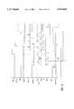
- FIG. 9shows a state diagram that provides a functional description of one-bit up/down counter 150.
- Counter 150receives as inputs an increment signal on line INC and a decrement signal on line DEC.
- commutation control circuit 50When commutation control circuit 50 is reset or develops a commutation pulse, counter 150 is reset to state 000.
- counter 150increments to state 001 and outputs a logic one on line LOCK -- 1.
- counter 150transitions to state 011. From state 011, counter 150 can either be decremented so that the signal on line LOCK -- 1 returns to zero, or incremented so that line LOCK -- 2 transitions to a logic one.
- FIG. 10shows a state diagram that provides a functional description of state machine 76.
- the inputs to state machine 76are the signals on nodes OVER -- H, UNDER -- L, SIGN, and FCOM.
- a logic one on node OVER -- Hindicates that the voltage on node V DLY is greater than the voltage on node V dac .
- a logic one on node UNDER -- L, the output of AND gate 157 of FIG. 8,indicates that:
- the count stored in up/down counter 150is greater than one, as evidenced by a logic one on line LOCK -- 1;
- a logic one on node SIGNindicates that the voltage on node POS is more positive than the voltage on node NEG.
- the time Z Crepresents the instant that the BEMF signal POS-NEG crosses the zero-voltage axis.
- the BEMF signal POS-NEGcrosses zero at other times due to noise; however, for purposes of the following description, the time Z C represents the true zero cross.
- Delay circuit 70operates to provide an FCOM pulse a delay period T DLY (i.e., a delay of one half the average FCOM period T FCOM ) after the zero cross at time Z C .
- State machine 76receives as inputs the digital (binary) signals on lines OVER -- H, UNDER -- L, SIGN, and FCOM, and outputs a digital signal on line UP to amplifier 72 and digital signals on increment line INC and decrement line DEC to counter 78. After each FCOM pulse (and when commutation control circuit 50 is reset or powered up), state machine 76 is reset to state 000 and counter circuit 78 is configured to store a count of zero. In state 000, state machine 76 outputs a logic one on line UP to amplifier 72. As explained above in connection with FIG.
- amplifier 72charges delay capacitance C DLY when the voltage on node POS is more positive than the voltage on node NEG, and discharges delay capacitance C DLY when the voltage on node POS is more negative than the voltage on node NEG.
- BEMF signal POS-NEGBefore the zero crossing at time Z C , BEMF signal POS-NEG will be negative in the absence of positive noise spikes. As such, the voltage on node V DLY will remain low.
- a noise spikesuch as spike 200
- the logic level on node SIGNwill change from low to high and the voltage on node V DLY will begin to increase.
- spike 200decreases to zero volts
- the logic level on node SIGNreturns to a logic low, causing the voltage on node V DLY to decrease.
- any negative noise spikes that go below zerowill reverse the direction of voltage change on node V DLY .
- the voltage on node V DLYdecreases along a negative-going segment 206.
- noise spike 204returns to a voltage greater than zero, the voltage on node V DLY will again increase.
- the voltage on node V DLYwill rise above the reference voltage on node V DAC causing comparator 74 to output a logic one on node OVER -- H.
- the inputs on nodes OVER -- H, UNDER -- L, and SIGNwill be 1, 0, and 1, respectively.
- state machine 76will cause state machine 76 to transition from state 000 to state 001 so that state machine 76 outputs a logic zero on line UP.
- providing a logic zero on the line UP to amplifier 72reverses the behavior of amplifier 72 with respect to BEMF signal POS-NEG. That is, when the voltage on node POS is more positive than that on node NEG, amplifier 72 discharges delay capacitor C DLY , causing the voltage on node V DLY to decrease. And, when the voltage on node POS is more negative than that on node NEG, amplifier 72 charges delay capacitor C DLY , causing the voltage on node V DLY to begin to increase.
- state machine 76Shortly after capacitance C DLY begins to discharge, the voltage on node V DLY will fall below the voltage on node V DAC so that the signal on node OVER -- H will return to a logic zero. Assuming that BEMF signal POS-NEG remains positive, state machine 76 will receive the inputs 0, 0, and 1 on input nodes OVER -- H, UNDER -- L, and SIGN, respectively, and will consequently move from state 001 to state 011. State machine 76 will then output a logic one on node INC causing the count stored in counter circuit 78 to increment. In the present case, the count increases from zero to one, as indicated by the signal COUNT of FIG. 11.
- state machine 76For brevity, only a few of the eight possible states of state machine 76 are described above. The remaining states, as shown in state diagram of FIG. 10, will be readily understood by those skilled in the art.
- Capacitance C DLYwill charge and discharge in the manner described above until the count stored by counter circuit 78 reaches a predetermined number.
- counter circuit 78is configured to issue an FCOM pulse when the count is four (i.e., the count of up/down counter 150 is two and the count of up counter 152 is two) and the signal on node UNDER -- L is one.
- the FCOM pulse on node FCOMis conveyed to sequencer 18 to initiate a commutation and also to reset both state machine 76 and counter circuit 78. The above-described process is then repeated for each subsequent zero cross so that an FCOM pulse is consistently developed after a delay of approximately 30 electrical degrees from each zero cross.
- Commutation delay generators in accordance with the present inventionare not limited to the particular applications described above.
- the electric motors that can benefit from such delay generatorsare not limited to disk drive motors.
- timing references from which to begin a delay periodmay be derived from sources other than BEMF sensors, such as Hall effect sensors. Therefore, the scope of the appended claims should not be limited to the description of the preferred versions described herein.
Landscapes
- Engineering & Computer Science (AREA)
- Power Engineering (AREA)
- Control Of Motors That Do Not Use Commutators (AREA)
Abstract
Description
Claims (17)
Priority Applications (3)
| Application Number | Priority Date | Filing Date | Title |
|---|---|---|---|
| US08/595,812US5767643A (en) | 1996-02-02 | 1996-02-02 | Commutation delay generator for a multiphase brushless DC motor |
| DE69736367TDE69736367T2 (en) | 1996-02-02 | 1997-01-27 | Time delay generator for the commutation of a multiphase brushless motor |
| EP97101208AEP0788221B1 (en) | 1996-02-02 | 1997-01-27 | Commutation delay generator for a multiphase brushless DC motor |
Applications Claiming Priority (1)
| Application Number | Priority Date | Filing Date | Title |
|---|---|---|---|
| US08/595,812US5767643A (en) | 1996-02-02 | 1996-02-02 | Commutation delay generator for a multiphase brushless DC motor |
Publications (1)
| Publication Number | Publication Date |
|---|---|
| US5767643Atrue US5767643A (en) | 1998-06-16 |
Family
ID=24384792
Family Applications (1)
| Application Number | Title | Priority Date | Filing Date |
|---|---|---|---|
| US08/595,812Expired - LifetimeUS5767643A (en) | 1996-02-02 | 1996-02-02 | Commutation delay generator for a multiphase brushless DC motor |
Country Status (3)
| Country | Link |
|---|---|
| US (1) | US5767643A (en) |
| EP (1) | EP0788221B1 (en) |
| DE (1) | DE69736367T2 (en) |
Cited By (17)
| Publication number | Priority date | Publication date | Assignee | Title |
|---|---|---|---|---|
| US5990643A (en)* | 1998-07-24 | 1999-11-23 | Advanced Motion Controls, Inc. | Sensorless commutation position detection for brushless D.C. motors |
| US6310450B1 (en)* | 1999-04-23 | 2001-10-30 | Stmicroelectronics S.R.L. | Drive system of a brushless motor equipped with hall sensors self-discriminating the actual phasing of the installed sensors |
| US6577085B2 (en) | 1998-02-11 | 2003-06-10 | Stmicroelectronics S.A. | Control of a brushless motor |
| US6906485B2 (en)* | 2001-11-05 | 2005-06-14 | Seagate Technology Llc | Spindle motor control using a current profile to taper current transitions |
| US20050168181A1 (en)* | 2004-01-29 | 2005-08-04 | Sanyo Electric Co., Ltd. | Motor drive apparatus, integrated circuit, and motor drive method |
| US7042668B1 (en) | 2000-11-07 | 2006-05-09 | Maxtor Corporation | Method and apparatus for generating an index location from a spin motor of a disk drive |
| US7106020B1 (en) | 2005-08-30 | 2006-09-12 | Honeywell International Inc. | Method of operating a brushless DC motor |
| US7265512B2 (en) | 2005-08-30 | 2007-09-04 | Honeywell International Inc. | Actuator with feedback for end stop positioning |
| US20080111512A1 (en)* | 2006-11-09 | 2008-05-15 | Honeywell International Inc. | Actuator position switch |
| US20080180047A1 (en)* | 2007-01-26 | 2008-07-31 | Stmicroelectronics, Inc. | Pair pole asymmetry compensation in back electromotive force zero cross detection |
| US20100066287A1 (en)* | 2008-09-15 | 2010-03-18 | Texas Instruments Incorporated | Systems and methods for detecting position for a brushless dc motor |
| US20100194326A1 (en)* | 2009-01-30 | 2010-08-05 | Honeywell International Inc. | Hvac actuator with internal heating |
| US7863842B1 (en)* | 2006-08-23 | 2011-01-04 | Marvell International Ltd. | Motor spindle control system and method |
| US8084982B2 (en) | 2008-11-18 | 2011-12-27 | Honeywell International Inc. | HVAC actuator with output torque compensation |
| US8283882B1 (en) | 2007-06-11 | 2012-10-09 | Marvell International Ltd. | Voice coil motor control system and method |
| US20140062360A1 (en)* | 2012-09-06 | 2014-03-06 | Sanyo Denki Co., Ltd. | Motor control device and motor control method |
| US20170338803A1 (en)* | 2016-05-20 | 2017-11-23 | Ultra Electronics Limited | Filter for a Brushless DC Motor |
Families Citing this family (3)
| Publication number | Priority date | Publication date | Assignee | Title |
|---|---|---|---|---|
| DE19860448A1 (en) | 1998-12-28 | 2000-06-29 | Grundfos A S Bjerringbro | Process for the commutation of an electronically commutated brushless multi-phase permanent magnet motor |
| EP1759987B1 (en)* | 2005-08-30 | 2011-03-30 | Torqeedo GmbH | Electric boat drive |
| CN108696207B (en)* | 2018-05-29 | 2020-11-10 | 美的威灵电机技术(上海)有限公司 | Control method and control system of high-speed brushless direct current motor |
Citations (29)
| Publication number | Priority date | Publication date | Assignee | Title |
|---|---|---|---|---|
| US4162435A (en)* | 1976-10-05 | 1979-07-24 | General Electric Company | Method and apparatus for electronically commutating a direct current motor without position sensors |
| US4250435A (en)* | 1980-01-04 | 1981-02-10 | General Electric Company | Clock rate control of electronically commutated motor rotational velocity |
| US4275343A (en)* | 1978-12-28 | 1981-06-23 | The Charles Stark Draper Laboratory, Inc. | Back EMF controlled permanent magnet motor |
| US4394610A (en)* | 1981-08-07 | 1983-07-19 | The United States Of America As Represented By The Administrator Of The National Aeronautics And Space Administration | Adaptive reference voltage generator for firing angle control of line-commutated inverters |
| US4401934A (en)* | 1981-08-07 | 1983-08-30 | The United States Of America As Represented By The Administrator Of The National Aeronautics And Space Administration | Adaptive control system for line-commutated inverters |
| US4455513A (en)* | 1982-07-26 | 1984-06-19 | Imec Corporation | Self-starting transducerless, brushless D.C. motor controller |
| US4513230A (en)* | 1980-04-17 | 1985-04-23 | General Electric Company | Laundering apparatus, method of operating a laundry machine, control system for an electronically commutated motor, and method of operating an electronically commutated motor |
| US4540906A (en)* | 1984-03-09 | 1985-09-10 | Synektron Corporation | Stator assembly for permanent magnet rotary device |
| US4575652A (en)* | 1984-09-27 | 1986-03-11 | Synektron Corporation | Permanent magnet motor having high starting torque and narrowly-defined detent zones |
| US4642537A (en)* | 1983-12-13 | 1987-02-10 | General Electric Company | Laundering apparatus |
| US4656400A (en)* | 1985-07-08 | 1987-04-07 | Synektron Corporation | Variable reluctance actuators having improved constant force control and position-sensing features |
| US4659969A (en)* | 1984-08-09 | 1987-04-21 | Synektron Corporation | Variable reluctance actuator having position sensing and control |
| US4665348A (en)* | 1984-08-09 | 1987-05-12 | Synektron Corporation | Method for sensing and controlling the position of a variable reluctance actuator |
| US4673849A (en)* | 1986-10-10 | 1987-06-16 | Allied Corporation | Permanent magnet motor closed loop restarting system |
| WO1988001763A1 (en)* | 1986-09-04 | 1988-03-10 | North Atlantic Industries, Inc. | Servo-system |
| US4743815A (en)* | 1987-09-01 | 1988-05-10 | Emerson Electric Co. | Brushless permanent magnet motor system |
| US4751459A (en)* | 1986-09-18 | 1988-06-14 | Synektron Corporation | Magnetic tachometer or accelerometer having highly permeable eddy current flux circuit |
| US4757241A (en)* | 1987-10-19 | 1988-07-12 | General Electric Company | PWM system for ECM motor |
| US4774428A (en)* | 1987-05-15 | 1988-09-27 | Synektron Corporation | Compact three-phase permanent magnet rotary machine having low vibration and high performance |
| US4928043A (en)* | 1988-11-14 | 1990-05-22 | Synektron Corporation | Back EMF sampling circuit for phase locked loop motor control |
| US4988939A (en)* | 1989-08-04 | 1991-01-29 | Thor Technology Corporation | Electric motor with variable commutation delay |
| US5015939A (en)* | 1990-08-10 | 1991-05-14 | Synektron Corporation | Control circuit for switched reluctance motor |
| US5034668A (en)* | 1989-12-04 | 1991-07-23 | Synektron Corporation | Control circuit for an electric motor |
| US5258695A (en)* | 1990-12-19 | 1993-11-02 | Integral Peripherals, Inc. | Spin motor control system for a hard disk assembly |
| US5272803A (en)* | 1993-02-05 | 1993-12-28 | Synektron Corporation | Method and apparatus for electric motor assembly with bearing preload |
| DE4231226A1 (en)* | 1992-09-18 | 1994-03-24 | Philips Patentverwaltung | Commutation circuitry for collectorless DC motor - with retardation circuit allowing shifting of commutation point by given delay interval |
| US5319289A (en)* | 1992-02-24 | 1994-06-07 | Silicon Systems, Inc. | Adaptive commutation delay for multi-pole brushless DC motors |
| JPH06253584A (en)* | 1993-02-24 | 1994-09-09 | Matsushita Electric Ind Co Ltd | Sensorless brushless motor drive |
| US5350988A (en)* | 1990-07-10 | 1994-09-27 | Alliedsignal, Inc. | Digital motor controller |
- 1996
- 1996-02-02USUS08/595,812patent/US5767643A/ennot_activeExpired - Lifetime
- 1997
- 1997-01-27DEDE69736367Tpatent/DE69736367T2/ennot_activeExpired - Lifetime
- 1997-01-27EPEP97101208Apatent/EP0788221B1/ennot_activeExpired - Lifetime
Patent Citations (30)
| Publication number | Priority date | Publication date | Assignee | Title |
|---|---|---|---|---|
| US4162435A (en)* | 1976-10-05 | 1979-07-24 | General Electric Company | Method and apparatus for electronically commutating a direct current motor without position sensors |
| US4275343A (en)* | 1978-12-28 | 1981-06-23 | The Charles Stark Draper Laboratory, Inc. | Back EMF controlled permanent magnet motor |
| US4250435A (en)* | 1980-01-04 | 1981-02-10 | General Electric Company | Clock rate control of electronically commutated motor rotational velocity |
| US4513230A (en)* | 1980-04-17 | 1985-04-23 | General Electric Company | Laundering apparatus, method of operating a laundry machine, control system for an electronically commutated motor, and method of operating an electronically commutated motor |
| US4394610A (en)* | 1981-08-07 | 1983-07-19 | The United States Of America As Represented By The Administrator Of The National Aeronautics And Space Administration | Adaptive reference voltage generator for firing angle control of line-commutated inverters |
| US4401934A (en)* | 1981-08-07 | 1983-08-30 | The United States Of America As Represented By The Administrator Of The National Aeronautics And Space Administration | Adaptive control system for line-commutated inverters |
| US4455513A (en)* | 1982-07-26 | 1984-06-19 | Imec Corporation | Self-starting transducerless, brushless D.C. motor controller |
| US4642537A (en)* | 1983-12-13 | 1987-02-10 | General Electric Company | Laundering apparatus |
| US4540906A (en)* | 1984-03-09 | 1985-09-10 | Synektron Corporation | Stator assembly for permanent magnet rotary device |
| US4659969A (en)* | 1984-08-09 | 1987-04-21 | Synektron Corporation | Variable reluctance actuator having position sensing and control |
| US4665348A (en)* | 1984-08-09 | 1987-05-12 | Synektron Corporation | Method for sensing and controlling the position of a variable reluctance actuator |
| US4575652A (en)* | 1984-09-27 | 1986-03-11 | Synektron Corporation | Permanent magnet motor having high starting torque and narrowly-defined detent zones |
| US4656400A (en)* | 1985-07-08 | 1987-04-07 | Synektron Corporation | Variable reluctance actuators having improved constant force control and position-sensing features |
| WO1988001763A1 (en)* | 1986-09-04 | 1988-03-10 | North Atlantic Industries, Inc. | Servo-system |
| US4751459A (en)* | 1986-09-18 | 1988-06-14 | Synektron Corporation | Magnetic tachometer or accelerometer having highly permeable eddy current flux circuit |
| US4673849A (en)* | 1986-10-10 | 1987-06-16 | Allied Corporation | Permanent magnet motor closed loop restarting system |
| US4774428A (en)* | 1987-05-15 | 1988-09-27 | Synektron Corporation | Compact three-phase permanent magnet rotary machine having low vibration and high performance |
| US4743815A (en)* | 1987-09-01 | 1988-05-10 | Emerson Electric Co. | Brushless permanent magnet motor system |
| US4757241A (en)* | 1987-10-19 | 1988-07-12 | General Electric Company | PWM system for ECM motor |
| US4928043A (en)* | 1988-11-14 | 1990-05-22 | Synektron Corporation | Back EMF sampling circuit for phase locked loop motor control |
| US4988939A (en)* | 1989-08-04 | 1991-01-29 | Thor Technology Corporation | Electric motor with variable commutation delay |
| US5034668A (en)* | 1989-12-04 | 1991-07-23 | Synektron Corporation | Control circuit for an electric motor |
| US5350988A (en)* | 1990-07-10 | 1994-09-27 | Alliedsignal, Inc. | Digital motor controller |
| US5015939A (en)* | 1990-08-10 | 1991-05-14 | Synektron Corporation | Control circuit for switched reluctance motor |
| US5258695A (en)* | 1990-12-19 | 1993-11-02 | Integral Peripherals, Inc. | Spin motor control system for a hard disk assembly |
| US5466997A (en)* | 1990-12-19 | 1995-11-14 | Integral Peripherals, Inc. | Spin motor control system for a hard disk assembly |
| US5319289A (en)* | 1992-02-24 | 1994-06-07 | Silicon Systems, Inc. | Adaptive commutation delay for multi-pole brushless DC motors |
| DE4231226A1 (en)* | 1992-09-18 | 1994-03-24 | Philips Patentverwaltung | Commutation circuitry for collectorless DC motor - with retardation circuit allowing shifting of commutation point by given delay interval |
| US5272803A (en)* | 1993-02-05 | 1993-12-28 | Synektron Corporation | Method and apparatus for electric motor assembly with bearing preload |
| JPH06253584A (en)* | 1993-02-24 | 1994-09-09 | Matsushita Electric Ind Co Ltd | Sensorless brushless motor drive |
Non-Patent Citations (2)
| Title |
|---|
| "Brushless DC Motor Drive Circuit", Philips Development Data, Jan. 1989. |
| Brushless DC Motor Drive Circuit , Philips Development Data , Jan. 1989.* |
Cited By (28)
| Publication number | Priority date | Publication date | Assignee | Title |
|---|---|---|---|---|
| US6577085B2 (en) | 1998-02-11 | 2003-06-10 | Stmicroelectronics S.A. | Control of a brushless motor |
| US5990643A (en)* | 1998-07-24 | 1999-11-23 | Advanced Motion Controls, Inc. | Sensorless commutation position detection for brushless D.C. motors |
| US6310450B1 (en)* | 1999-04-23 | 2001-10-30 | Stmicroelectronics S.R.L. | Drive system of a brushless motor equipped with hall sensors self-discriminating the actual phasing of the installed sensors |
| US7042668B1 (en) | 2000-11-07 | 2006-05-09 | Maxtor Corporation | Method and apparatus for generating an index location from a spin motor of a disk drive |
| US6906485B2 (en)* | 2001-11-05 | 2005-06-14 | Seagate Technology Llc | Spindle motor control using a current profile to taper current transitions |
| US20050168181A1 (en)* | 2004-01-29 | 2005-08-04 | Sanyo Electric Co., Ltd. | Motor drive apparatus, integrated circuit, and motor drive method |
| US7053573B2 (en)* | 2004-01-29 | 2006-05-30 | Sanyo Electric Co., Ltd. | Motor drive apparatus, integrated circuit, and motor drive method |
| US7106020B1 (en) | 2005-08-30 | 2006-09-12 | Honeywell International Inc. | Method of operating a brushless DC motor |
| US7265512B2 (en) | 2005-08-30 | 2007-09-04 | Honeywell International Inc. | Actuator with feedback for end stop positioning |
| US7863842B1 (en)* | 2006-08-23 | 2011-01-04 | Marvell International Ltd. | Motor spindle control system and method |
| US8314581B1 (en) | 2006-08-23 | 2012-11-20 | Marvell International Ltd. | Motor spindle control system and method |
| US8497647B1 (en) | 2006-08-23 | 2013-07-30 | Marvell International Ltd. | Motor spindle control system and method |
| US20080111512A1 (en)* | 2006-11-09 | 2008-05-15 | Honeywell International Inc. | Actuator position switch |
| US7586279B2 (en) | 2006-11-09 | 2009-09-08 | Honeywell International Inc. | Actuator position switch |
| US20110127939A1 (en)* | 2007-01-26 | 2011-06-02 | Stmicroelectronics, Inc. | Pair pole asymmetry compensation in back electromotive force zero cross detection |
| US20080180047A1 (en)* | 2007-01-26 | 2008-07-31 | Stmicroelectronics, Inc. | Pair pole asymmetry compensation in back electromotive force zero cross detection |
| US7893643B2 (en)* | 2007-01-26 | 2011-02-22 | Stmicroelectronics, Inc. | Pair pole asymmetry compensation in back electromotive force zero cross detection |
| US8593096B1 (en) | 2007-06-11 | 2013-11-26 | Marvell International Ltd. | Voice coil motor control system and method |
| US8283882B1 (en) | 2007-06-11 | 2012-10-09 | Marvell International Ltd. | Voice coil motor control system and method |
| US8237385B2 (en)* | 2008-09-15 | 2012-08-07 | Texas Instruments Incorporated | Systems and methods for detecting position for a brushless DC motor |
| US20100066287A1 (en)* | 2008-09-15 | 2010-03-18 | Texas Instruments Incorporated | Systems and methods for detecting position for a brushless dc motor |
| US8084982B2 (en) | 2008-11-18 | 2011-12-27 | Honeywell International Inc. | HVAC actuator with output torque compensation |
| US8084980B2 (en) | 2009-01-30 | 2011-12-27 | Honeywell International Inc. | HVAC actuator with internal heating |
| US20100194326A1 (en)* | 2009-01-30 | 2010-08-05 | Honeywell International Inc. | Hvac actuator with internal heating |
| US20140062360A1 (en)* | 2012-09-06 | 2014-03-06 | Sanyo Denki Co., Ltd. | Motor control device and motor control method |
| US9246422B2 (en)* | 2012-09-06 | 2016-01-26 | Sanyo Denki Co., Ltd. | Motor control device and motor control method |
| US20170338803A1 (en)* | 2016-05-20 | 2017-11-23 | Ultra Electronics Limited | Filter for a Brushless DC Motor |
| US10361682B2 (en)* | 2016-05-20 | 2019-07-23 | Ultra Electronics Limited | Filter for a brushless DC motor |
Also Published As
| Publication number | Publication date |
|---|---|
| DE69736367T2 (en) | 2007-07-19 |
| EP0788221B1 (en) | 2006-07-26 |
| EP0788221A1 (en) | 1997-08-06 |
| DE69736367D1 (en) | 2006-09-07 |
Similar Documents
| Publication | Publication Date | Title |
|---|---|---|
| US5767643A (en) | Commutation delay generator for a multiphase brushless DC motor | |
| US5317243A (en) | Method and apparatus for detecting velocity profiles of a spinning rotor of a polyphase DC motor | |
| US5294877A (en) | Circuit and method for detecting deceleration rates of a polyphase DC motor | |
| EP0316077B1 (en) | Brushless motors | |
| US5767639A (en) | Electronic control system for a brushless electric motor | |
| US20100295490A1 (en) | Motor drive apparatus and motor drive method | |
| US6724166B2 (en) | Apparatus for reducing motor driving noise and method for generating motor driving noise reducing signal | |
| CN109905060B (en) | Semiconductor devices, motor drive systems, and motor control programs | |
| JP2000287477A (en) | Motor drive | |
| WO1992011687A2 (en) | Spin motor control system for a hard disk assembly | |
| WO2011109435A2 (en) | Position corrected pulse width modulation for brushless direct current motors | |
| US4507591A (en) | Linear pulse width to current converter for brushless DC motors | |
| KR100288770B1 (en) | Rectifier Circuit for Sensorless Three-Phase Bieldi Motors | |
| US7190145B2 (en) | Method and apparatus for improving speed measurement quality in multi-pole machines | |
| US5990656A (en) | Frequency detector | |
| TWI435532B (en) | Soft-switching control citcuit for dc motor | |
| JPH11299283A (en) | Sensorless motor driver | |
| US6249096B1 (en) | Apparatus and method for determining commutation time of sensorless brushless direct current (BLDC) motor | |
| JPH0343866B2 (en) | ||
| JP2897210B2 (en) | Sensorless drive for brushless motor | |
| KR0177991B1 (en) | A commutating triggering circuit of sensorless bldc motor | |
| US6066929A (en) | Frequency generator circuit for a brushless DC motor control system | |
| JP2002125388A (en) | Motor driver | |
| JP2751608B2 (en) | Commutatorless DC motor | |
| JPH04190658A (en) | Dc motor |
Legal Events
| Date | Code | Title | Description |
|---|---|---|---|
| AS | Assignment | Owner name:SILICONIX INCORPORATED, CALIFORNIA Free format text:ASSIGNMENT OF ASSIGNORS INTEREST;ASSIGNORS:PHAM, GIAO M.;CONCKLIN, BARRY J.;NGUYEN, JAMES H.;REEL/FRAME:007996/0455 Effective date:19960514 | |
| STCF | Information on status: patent grant | Free format text:PATENTED CASE | |
| FPAY | Fee payment | Year of fee payment:4 | |
| REMI | Maintenance fee reminder mailed | ||
| FPAY | Fee payment | Year of fee payment:8 | |
| FPAY | Fee payment | Year of fee payment:12 | |
| AS | Assignment | Owner name:COMERICA BANK, AS AGENT,MICHIGAN Free format text:SECURITY AGREEMENT;ASSIGNORS:VISHAY SPRAGUE, INC., SUCCESSOR IN INTEREST TO VISHAY EFI, INC. AND VISHAY THIN FILM, LLC;VISHAY DALE ELECTRONICS, INC.;VISHAY INTERTECHNOLOGY, INC.;AND OTHERS;REEL/FRAME:024006/0515 Effective date:20100212 Owner name:COMERICA BANK, AS AGENT, MICHIGAN Free format text:SECURITY AGREEMENT;ASSIGNORS:VISHAY SPRAGUE, INC., SUCCESSOR IN INTEREST TO VISHAY EFI, INC. AND VISHAY THIN FILM, LLC;VISHAY DALE ELECTRONICS, INC.;VISHAY INTERTECHNOLOGY, INC.;AND OTHERS;REEL/FRAME:024006/0515 Effective date:20100212 | |
| AS | Assignment | Owner name:VISHAY INTERTECHNOLOGY, INC., A DELAWARE CORPORATI Free format text:RELEASE BY SECURED PARTY;ASSIGNOR:COMERICA BANK, AS AGENT, A TEXAS BANKING ASSOCIATION (FORMERLY A MICHIGAN BANKING CORPORATION);REEL/FRAME:025489/0184 Effective date:20101201 Owner name:SILICONIX INCORPORATED, A DELAWARE CORPORATION, PE Free format text:RELEASE BY SECURED PARTY;ASSIGNOR:COMERICA BANK, AS AGENT, A TEXAS BANKING ASSOCIATION (FORMERLY A MICHIGAN BANKING CORPORATION);REEL/FRAME:025489/0184 Effective date:20101201 Owner name:VISHAY VITRAMON, INCORPORATED, A DELAWARE CORPORAT Free format text:RELEASE BY SECURED PARTY;ASSIGNOR:COMERICA BANK, AS AGENT, A TEXAS BANKING ASSOCIATION (FORMERLY A MICHIGAN BANKING CORPORATION);REEL/FRAME:025489/0184 Effective date:20101201 Owner name:VISHAY MEASUREMENTS GROUP, INC., A DELAWARE CORPOR Free format text:RELEASE BY SECURED PARTY;ASSIGNOR:COMERICA BANK, AS AGENT, A TEXAS BANKING ASSOCIATION (FORMERLY A MICHIGAN BANKING CORPORATION);REEL/FRAME:025489/0184 Effective date:20101201 Owner name:VISHAY GENERAL SEMICONDUCTOR, LLC, F/K/A GENERAL S Free format text:RELEASE BY SECURED PARTY;ASSIGNOR:COMERICA BANK, AS AGENT, A TEXAS BANKING ASSOCIATION (FORMERLY A MICHIGAN BANKING CORPORATION);REEL/FRAME:025489/0184 Effective date:20101201 Owner name:VISHAY DALE ELECTRONICS, INC., A DELAWARE CORPORAT Free format text:RELEASE BY SECURED PARTY;ASSIGNOR:COMERICA BANK, AS AGENT, A TEXAS BANKING ASSOCIATION (FORMERLY A MICHIGAN BANKING CORPORATION);REEL/FRAME:025489/0184 Effective date:20101201 Owner name:VISHAY SPRAGUE, INC., SUCCESSOR-IN-INTEREST TO VIS Free format text:RELEASE BY SECURED PARTY;ASSIGNOR:COMERICA BANK, AS AGENT, A TEXAS BANKING ASSOCIATION (FORMERLY A MICHIGAN BANKING CORPORATION);REEL/FRAME:025489/0184 Effective date:20101201 Owner name:YOSEMITE INVESTMENT, INC., AN INDIANA CORPORATION, Free format text:RELEASE BY SECURED PARTY;ASSIGNOR:COMERICA BANK, AS AGENT, A TEXAS BANKING ASSOCIATION (FORMERLY A MICHIGAN BANKING CORPORATION);REEL/FRAME:025489/0184 Effective date:20101201 | |
| AS | Assignment | Owner name:JPMORGAN CHASE BANK, N.A., AS ADMINISTRATIVE AGENT, TEXAS Free format text:SECURITY AGREEMENT;ASSIGNORS:VISHAY INTERTECHNOLOGY, INC.;VISHAY DALE ELECTRONICS, INC.;SILICONIX INCORPORATED;AND OTHERS;REEL/FRAME:025675/0001 Effective date:20101201 Owner name:JPMORGAN CHASE BANK, N.A., AS ADMINISTRATIVE AGENT Free format text:SECURITY AGREEMENT;ASSIGNORS:VISHAY INTERTECHNOLOGY, INC.;VISHAY DALE ELECTRONICS, INC.;SILICONIX INCORPORATED;AND OTHERS;REEL/FRAME:025675/0001 Effective date:20101201 | |
| AS | Assignment | Owner name:VISHAY DALE ELECTRONICS, INC., NEBRASKA Free format text:RELEASE BY SECURED PARTY;ASSIGNOR:JPMORGAN CHASE BANK, N.A., AS ADMINISTRATIVE AGENT;REEL/FRAME:049826/0312 Effective date:20190716 Owner name:VISHAY VITRAMON, INC., VERMONT Free format text:RELEASE BY SECURED PARTY;ASSIGNOR:JPMORGAN CHASE BANK, N.A., AS ADMINISTRATIVE AGENT;REEL/FRAME:049826/0312 Effective date:20190716 Owner name:VISHAY EFI, INC., VERMONT Free format text:RELEASE BY SECURED PARTY;ASSIGNOR:JPMORGAN CHASE BANK, N.A., AS ADMINISTRATIVE AGENT;REEL/FRAME:049826/0312 Effective date:20190716 Owner name:VISHAY TECHNO COMPONENTS, LLC, VERMONT Free format text:RELEASE BY SECURED PARTY;ASSIGNOR:JPMORGAN CHASE BANK, N.A., AS ADMINISTRATIVE AGENT;REEL/FRAME:049826/0312 Effective date:20190716 Owner name:DALE ELECTRONICS, INC., NEBRASKA Free format text:RELEASE BY SECURED PARTY;ASSIGNOR:JPMORGAN CHASE BANK, N.A., AS ADMINISTRATIVE AGENT;REEL/FRAME:049826/0312 Effective date:20190716 Owner name:VISHAY INTERTECHNOLOGY, INC., PENNSYLVANIA Free format text:RELEASE BY SECURED PARTY;ASSIGNOR:JPMORGAN CHASE BANK, N.A., AS ADMINISTRATIVE AGENT;REEL/FRAME:049826/0312 Effective date:20190716 Owner name:SILICONIX INCORPORATED, CALIFORNIA Free format text:RELEASE BY SECURED PARTY;ASSIGNOR:JPMORGAN CHASE BANK, N.A., AS ADMINISTRATIVE AGENT;REEL/FRAME:049826/0312 Effective date:20190716 Owner name:SPRAGUE ELECTRIC COMPANY, VERMONT Free format text:RELEASE BY SECURED PARTY;ASSIGNOR:JPMORGAN CHASE BANK, N.A., AS ADMINISTRATIVE AGENT;REEL/FRAME:049826/0312 Effective date:20190716 Owner name:VISHAY SPRAGUE, INC., VERMONT Free format text:RELEASE BY SECURED PARTY;ASSIGNOR:JPMORGAN CHASE BANK, N.A., AS ADMINISTRATIVE AGENT;REEL/FRAME:049826/0312 Effective date:20190716 |