US5765203A - Storage and addressing method for a buffer memory control system for accessing user and error imformation - Google Patents
Storage and addressing method for a buffer memory control system for accessing user and error imformationDownload PDFInfo
- Publication number
- US5765203A US5765203AUS08/574,669US57466995AUS5765203AUS 5765203 AUS5765203 AUS 5765203AUS 57466995 AUS57466995 AUS 57466995AUS 5765203 AUS5765203 AUS 5765203A
- Authority
- US
- United States
- Prior art keywords
- information data
- column address
- address
- user information
- error information
- Prior art date
- Legal status (The legal status is an assumption and is not a legal conclusion. Google has not performed a legal analysis and makes no representation as to the accuracy of the status listed.)
- Expired - Lifetime
Links
Images


Classifications
- G—PHYSICS
- G06—COMPUTING OR CALCULATING; COUNTING
- G06F—ELECTRIC DIGITAL DATA PROCESSING
- G06F11/00—Error detection; Error correction; Monitoring
- G06F11/07—Responding to the occurrence of a fault, e.g. fault tolerance
- G06F11/08—Error detection or correction by redundancy in data representation, e.g. by using checking codes
- G06F11/10—Adding special bits or symbols to the coded information, e.g. parity check, casting out 9's or 11's
- G06F11/1008—Adding special bits or symbols to the coded information, e.g. parity check, casting out 9's or 11's in individual solid state devices
Definitions
- This inventionrelates to memory systems and, more particularly, to methods for controlling buffer memory systems for magnetic disc memory systems.
- Temporary storage devicessuch as dynamic random access memory devices, DRAMS, are often used in connection with magnetic storage media as buffer memories for temporarily storing character information. Each character is represented, for example, by an 8-bit information word and one parity bit. Typically, information is read into a temporary storage memory device one character at a time, using 9 parallel data bit lines.
- DRAMSare typically available as 1 bit, 2 bit, 8 bit, or 16 bit wide devices so that storage of the extra parity bit associated with each character word is cumbersome, resulting in the parity bit not being stored or being stored in separate memory device. In the alternative, DRAMS with provision for parity bit tend to be too expensive.
- FIG. 1shows the layout of data bits and parity according to the teachings of U.S. Pat. No. 5,280,601.
- FIG. 2 and FIG. 3show associated timing cycles involved.
- FIG. 1diagramatically shows storage of data and parity information in a buffer memory 10 consisting of a controller 10a and DRAM 17.
- the datais received from host 11 along SCSI bus 12 and stored in DRAM 17.
- Data stored in DRAM 17is later transferred to a disc memory 13 along disc memory bus 14.
- Information from the host FIFO 15is inputted to the DRAM 17 in 16 byte blocks of data. Parity for that block is generated by the parity generator 18 and stored in the parity storage area 19 of the DRAM 17 while 16 byte blocks of data is written in the data storage 20 of the DRAM.
- the datais readout both from the parity storage area 19 and the data storage area 20 of the DRAM 17 into the form FIFO 21.
- Parity checking on the output data being readout from the DRAM 17is performed by the parity checker 22. Parity is generated during write mode and it is checked during the read mode. Parity is written in a separate place in the DRAM requiring 2K bytes of address space for parity storage area 19 for every 32K bytes of total memory.
- the controller 10afurther generates appropriate control signals RAS 23 or CAS 24, when the address lines 25 have row address or column address respectively. Further, the controller generates appropriate control signals G or W depending upon read mode or a write mode.
- the transfer sequence for a block of 32 bytes of data to a normal page mode DRAMis shown in FIG. 2.
- the row addressis presented.
- 32 columns of dataare transferred.
- the parity row addressis presented followed by the parity information from the two parity columns.
- the corresponding data column precharge and parity row and parity column precharge cyclesare also shown in FIG. 2.
- FIG. 3The transfer sequence for a block of 32 bytes of data to a static column mode DRAM is shown in FIG. 3. If a single static-column mode DRAM is used, the information from a column is transferred one after another, without need for intervening precharge cycles.
- the FIG. 3also shows necessary parity row precharge cycle prior to the application of parity row address.
- the data and corresponding parityare stored at separate locations in a DRAM, with different row addresses.
- parity row precharge cyclesin addition to parity row address cycle is needed before parity column address can be applied.
- the data blocksare always followed by parity data.
- the method of storing parity data in a different rowadds additional clock cycles before parity data is written or read after the associated data is written or read.
- an address generation circuit to calculate corresponding row address for parity datawill be dependent upon the row/column organization of the DRAM configuration used and the number of bytes of data stored in a column. This constraint on address generation circuit practically leading to a limitation of using a predetermined types of DRAM configurations.
- the present inventionprovides a controller for DRAM buffer memories for a magnetic disc storage system, where the controller provides for efficient use of low cost standard DRAM memories to store user information data and error information data, with improved cycle time for completion of a read cycle or a write cycle.
- a method of storing and retrieving P user information data and Q error information data for said P user information data in a buffer memory unit having multiple DRAMsis disclosed.
- P user information data and Q error information datatogether define a paragraph.
- Each user information datahas a plurality of information units.
- Each error information datahas a plurality of information units.
- Each DRAMhas a plurality of rows and columns, with a maximum column address of M and each row capable of storing N such paragraphs.
- the virtual memory address for each user information datais translated to corresponding addresses of memory locations by selecting a row address, selecting a base column address and successively incrementing the base column address to provide additional column addresses for successive user information data.
- the virtual memory addressis further translated to corresponding addresses of memory locations for error information data by retaining the row address determined by the translating step for corresponding user information data, selecting a starting base column address for the error information data and successively decrementing the starting base column address to provide additional column addresses for successive error information data.
- the method of selecting a row address for the user information dataincludes the steps of dividing the virtual memory address by N the number of paragraphs per row, then assigning quotient of the division as the row address and assigning remainder of the division as the starting base column address for the user information data.
- the base column addressis incremented from (starting base column address+0) to (starting base column address+P).
- the method of selecting a column address for the error information data when the number of error information data per paragraph is oneincludes the steps of subtracting starting base column address of corresponding user information data from M the maximum column address and assigning result as the column address for error information data.
- FIG. 1shows the layout of data bits and parity according to the teachings of prior art implementation.
- FIG. 2shows timing cycles associated with the prior art implementation as shown in FIG. 1 for a normal page mode DRAM.
- FIG. 3shows timing cycles associated with the prior art implementation as shown in FIG. 1 for a static column mode DRAM.
- FIG. 4shows the layout of user information data and en or information data according to the teachings of the current implementation.
- FIG. 5shows virtual memory address with corresponding addresses for user information data and error information data for the layout shown in FIG. 4.
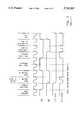
- FIG. 6shows a block diagram for logical implementation of the preferred embodiment.
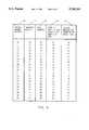
- FIG. 4there is shown a buffer memory unit with 16 ⁇ 16 bytes, with each byte having 4 bits of information units.
- the buffer memory unithas 16 row addresses and 16 column addresses, to address one out of 256 bytes of memory. Sixteen row address 45 are shown in the figure.
- Each row of buffer memorystore 3 paragraphs 31, 32 and 33 of information, each paragraph 31, 32 and 33 containing four bytes 34, 35, 36 and 37 of user information data and one byte of error information data 38.
- the starting base column address for user information data portion 39 of paragraphs 31, 32 and 33is 0, 1 and 2 respectively.
- the corresponding starting base column address for error information data 40for respective paragraphs being 15, 14 and 13.
- Individual user information data bytes 34, 35, 36 or 37 within a paragraph 31, 32 or 33is addressed by adding corresponding user information byte address 41 to the starting base column address for user information data 39.
- the maximum column address of the buffer memory unit as shownis 15.
- the corresponding column address for error information data 40is 15, 14 and 13 respectively.
- a virtual memory address 43 with a value of 6is received and divided by 3, the number of paragraphs per row.
- the quotient 2is assigned to the row address 45 and remainder 0 is assigned to the starting base column address for user information data 39 for paragraph 6.
- the column address for the error information data 40 for paragraph 6is determined by subtracting 0, the starting base column address for user information data 39 for paragraph 6, from 15, the maximum column address of the buffer memory unit, yielding 15 as the column address for the error information data 40 for paragraph 6.
- Successive user information data bytes within paragraph 6is addressed by adding the corresponding user information byte addresses 41 to starting base column address for user information data 39 of 0.
- each paragraphcontains only one byte of error information data.
- the virtual memory addressis presented as A inputs to first Mux 50 and second Mux 51, with Mux 50 receiving bits 0-11 and second Mux 51 receiving bits 12-19.
- the output of first Mux 50is connected to the input of first flip-flop bank 52 via first input bus 53.
- the output of second Mux 51is connected to the A input of third Mux 54.
- the output of third Mux 54is connected to the input of second flip-flop bank 55 via second input bus 56.
- second flip-flop bank 55 and the output of Bridge flip-flop 77are connected to second output bus 57, which routes the outputs to B input of first adder 58, B input of first comparator 59, B input of third Mux 54 and input of column address register 60.
- the paragraph per row 73is loaded to a devisor register 61. and output of the divisor register 61 is provided as the A input of first adder 58 and first comparator 59.
- the output of first adder 58is provided as the B input of second Mux 51.
- the A greater than B and A equal to B outputs of first comparator 59 as quotient trainis fed as the input to spare flip-flop 62 and as one of the select inputs to third Mux 54, through an OR gate 83.
- the output of spare flip-flop 62 and the first flip-flop bank 52 except Bridge flip-flop 77is connected to first output bus 63, which routes the outputs to B input of first Mux 50 and input of row address register 64.
- the Q counter 65counts the completion of division cycle and P counter 66 counts the number of column addresses presented at the output of fifth Mux 67.
- the output of row address register 64is fed as A input of fourth Mux 68 and the output of base column address register 60 is fed as most significant bits of first column address counter 79, with user byte count register 84 loading starting byte address as the least significant bits.
- the output of the first column address counter 79is fed as B input of fourth Mux D 68.
- Inverted output of base column address register 60is fed as A input of second adder 69.
- Maximum column address 74is fed as B input of second adder 69.
- the output of fourth Mux 68is fed as A input of fifth Mux 67.
- the output of second adder 69is fed as most significant bits of second column address counter 69, with error byte count register 85 loading starting byte address as the least significant bits.
- the output of second column address counter 80is fed as B input of fifth Mux 67.
- the output of fifth Mux 67present the decoded row, column and parity column address.
- the load row 70 output of Q counter 65enables the loading of row address register 64, when the row address is available on first output bus 63.
- the load column output 71 of Q counter 65enables the loading of column address register 60, when the column address is available on second output bus 57.
- the load column 71 outputalso enables the counting of P counter 66 to start counting the number of column addresses presented at the output of fifth Mux 67 and selection of A/B input of fourth Mux 68.
- the output PCOL Sel 72 of P counter 66enables the selection of A/B output of fifth Mux 67.
- the user byte increment 81 signal of P counter 66increments the first column address counter 79.
- the virtual memory address 75, paragraphs per row 73 as divisor and maximum column address 74are presented as input to first Mux 50 and second Mux 51, first adder 58 and second adder 69.
- the number of user information data bytes per paragraphare loaded into user byte count register 84.
- load signal 76is applied. This enables the selection of A input of first Mux 50, second Mux 51, and third Mux 54. This also enables the Q counter 65.
- Respective address bitsare then presented as inputs to the first flip-flop bank 52 and second flip-flop bank 55
- the outputs of second flip-flop bank 55which is the most significant 10 bits of the virtual memory address 75 is presented as dividend at the B input of the first adder 58, B input of comparator 59 and B input of third Mux 54.
- the output of the first adder 58 through the B input of second Mux 51is available as the A input of third Mux 54. If the dividend was greater than or equal to the divisor, a quotient of 1 is received on the output of first comparator 59. If the dividend was less than the divisor, a quotient of 0 is received. The quotient of 1 further enables the selection of A input of third Mux 54.
- the remainder of the divisionis available as the output of first adder 58, which will be presented as the A input of third Mux 54, thereby loading the remainder of the division into second flip-flop bank 55. Further, the quotient is stored in the Spare flip-flop 62. During the next clock cycle, the contents of all the flip-flops in first flip-flop bank 52 and second flip-flop bank 55 are shifted to the right and another division cycle occurs. Upon completion of 12 such division cycles, the quotient of the division is available in first flip flop bank 52 and the Spare flip-flop 62, except the bridge flip-flop 76. The Spare flip-flop 62 containing the least significant bit of the quotient. Further, the remainder is available in Bridge flip-flop 77 and second flip-flop bank 55, with Bridge flip-flop 77 containing the least significant bit of the quotient.
- the quotientwhich is the row address is available as the input to row address register 64.
- Q counter 65issues a load row 70 signal, enabling the latching of row address and initiates the P counter 66 by issuing a start P count 78 signal.
- the row addressis enabled at the output of fifth Mux 67, via the A input of fourth Mux 68.
- the Q counterissues a load column 71 signal, which latches in the base column address available at the input of base column address register 60.
- the output of base column address register 60is fed as the most significant bits of first column address counter 79.
- the base column address and maximum column address 74are presented as inputs to second adder 69 and the difference as column address for error information data is available at the output of second adder 69.
- first column address counter 79is available as the B input of fourth Mux 68.
- the load column 71 signal of Q counter 65enables the selection of B input of fourth Mux 68.
- the user byte increment 81 signal from P counter 66 to the first column address counter 79successively increments the column address to provide successive user information data column addresses as the A input of fifth Mux 67 and available at the output of fifth Mux 67.
- the P counter 66After incrementing successive user information data column address, the P counter 66 issues a PCOL Sel 72 signal which will enable the selection of B input of fifth Mux 67, thus presenting the column address for error information data at the output of fifth Mux 67.
- the error information datacould be parity information or could be any other type of error detection or error correction data. Further, depending upon the type of error information data, one or more number of bytes of error information data may be necessary for a given number of bytes of user information data.
- the disclosed methodcan be easily implemented in DRAM configurations of any rows and columns, provided the width of the DRAM is at least 2(P+Q), with a simple means for translating a given virtual memory address to corresponding address for user information data and error information data.
Landscapes
- Engineering & Computer Science (AREA)
- Theoretical Computer Science (AREA)
- Quality & Reliability (AREA)
- Physics & Mathematics (AREA)
- General Engineering & Computer Science (AREA)
- General Physics & Mathematics (AREA)
- Dram (AREA)
Abstract
Description
Claims (7)
Priority Applications (1)
| Application Number | Priority Date | Filing Date | Title |
|---|---|---|---|
| US08/574,669US5765203A (en) | 1995-12-19 | 1995-12-19 | Storage and addressing method for a buffer memory control system for accessing user and error imformation |
Applications Claiming Priority (1)
| Application Number | Priority Date | Filing Date | Title |
|---|---|---|---|
| US08/574,669US5765203A (en) | 1995-12-19 | 1995-12-19 | Storage and addressing method for a buffer memory control system for accessing user and error imformation |
Publications (1)
| Publication Number | Publication Date |
|---|---|
| US5765203Atrue US5765203A (en) | 1998-06-09 |
Family
ID=24297114
Family Applications (1)
| Application Number | Title | Priority Date | Filing Date |
|---|---|---|---|
| US08/574,669Expired - LifetimeUS5765203A (en) | 1995-12-19 | 1995-12-19 | Storage and addressing method for a buffer memory control system for accessing user and error imformation |
Country Status (1)
| Country | Link |
|---|---|
| US (1) | US5765203A (en) |
Cited By (19)
| Publication number | Priority date | Publication date | Assignee | Title |
|---|---|---|---|---|
| US20090285031A1 (en)* | 2005-06-24 | 2009-11-19 | Suresh Natarajan Rajan | System and method for simulating an aspect of a memory circuit |
| EP2696290A1 (en)* | 2006-02-09 | 2014-02-12 | Google Inc. | Memory circuit system and method |
| US8710862B2 (en) | 2009-06-09 | 2014-04-29 | Google Inc. | Programming of DIMM termination resistance values |
| US8751732B2 (en) | 2006-10-05 | 2014-06-10 | Google Inc. | System and method for increasing capacity, performance, and flexibility of flash storage |
| US8762675B2 (en) | 2008-06-23 | 2014-06-24 | Google Inc. | Memory system for synchronous data transmission |
| US8760936B1 (en) | 2006-11-13 | 2014-06-24 | Google Inc. | Multi-rank partial width memory modules |
| US8773937B2 (en) | 2005-06-24 | 2014-07-08 | Google Inc. | Memory refresh apparatus and method |
| US8776049B2 (en) | 2004-10-20 | 2014-07-08 | Seagate Technology Llc | Address aligned resource set allocation in a memory space |
| US8797779B2 (en) | 2006-02-09 | 2014-08-05 | Google Inc. | Memory module with memory stack and interface with enhanced capabilites |
| US8811065B2 (en) | 2005-09-02 | 2014-08-19 | Google Inc. | Performing error detection on DRAMs |
| US8819356B2 (en) | 2008-07-25 | 2014-08-26 | Google Inc. | Configurable multirank memory system with interface circuit |
| US8868829B2 (en) | 2006-07-31 | 2014-10-21 | Google Inc. | Memory circuit system and method |
| US8972673B2 (en) | 2006-07-31 | 2015-03-03 | Google Inc. | Power management of memory circuits by virtual memory simulation |
| US8977806B1 (en) | 2006-10-05 | 2015-03-10 | Google Inc. | Hybrid memory module |
| US9047976B2 (en) | 2006-07-31 | 2015-06-02 | Google Inc. | Combined signal delay and power saving for use with a plurality of memory circuits |
| US9171585B2 (en) | 2005-06-24 | 2015-10-27 | Google Inc. | Configurable memory circuit system and method |
| US9507739B2 (en) | 2005-06-24 | 2016-11-29 | Google Inc. | Configurable memory circuit system and method |
| US9632929B2 (en) | 2006-02-09 | 2017-04-25 | Google Inc. | Translating an address associated with a command communicated between a system and memory circuits |
| US10013371B2 (en) | 2005-06-24 | 2018-07-03 | Google Llc | Configurable memory circuit system and method |
Citations (5)
| Publication number | Priority date | Publication date | Assignee | Title |
|---|---|---|---|---|
| US4918645A (en)* | 1987-09-17 | 1990-04-17 | Wang Laboratories, Inc. | Computer bus having page mode memory access |
| US5034917A (en)* | 1988-05-26 | 1991-07-23 | Bland Patrick M | Computer system including a page mode memory with decreased access time and method of operation thereof |
| US5127014A (en)* | 1990-02-13 | 1992-06-30 | Hewlett-Packard Company | Dram on-chip error correction/detection |
| US5280601A (en)* | 1990-03-02 | 1994-01-18 | Seagate Technology, Inc. | Buffer memory control system for a magnetic disc controller |
| US5303364A (en)* | 1989-09-29 | 1994-04-12 | Compaq Computer Corp. | Paged memory controller |
- 1995
- 1995-12-19USUS08/574,669patent/US5765203A/ennot_activeExpired - Lifetime
Patent Citations (5)
| Publication number | Priority date | Publication date | Assignee | Title |
|---|---|---|---|---|
| US4918645A (en)* | 1987-09-17 | 1990-04-17 | Wang Laboratories, Inc. | Computer bus having page mode memory access |
| US5034917A (en)* | 1988-05-26 | 1991-07-23 | Bland Patrick M | Computer system including a page mode memory with decreased access time and method of operation thereof |
| US5303364A (en)* | 1989-09-29 | 1994-04-12 | Compaq Computer Corp. | Paged memory controller |
| US5127014A (en)* | 1990-02-13 | 1992-06-30 | Hewlett-Packard Company | Dram on-chip error correction/detection |
| US5280601A (en)* | 1990-03-02 | 1994-01-18 | Seagate Technology, Inc. | Buffer memory control system for a magnetic disc controller |
Cited By (20)
| Publication number | Priority date | Publication date | Assignee | Title |
|---|---|---|---|---|
| US8776049B2 (en) | 2004-10-20 | 2014-07-08 | Seagate Technology Llc | Address aligned resource set allocation in a memory space |
| US8949519B2 (en) | 2005-06-24 | 2015-02-03 | Google Inc. | Simulating a memory circuit |
| US10013371B2 (en) | 2005-06-24 | 2018-07-03 | Google Llc | Configurable memory circuit system and method |
| US9507739B2 (en) | 2005-06-24 | 2016-11-29 | Google Inc. | Configurable memory circuit system and method |
| US9171585B2 (en) | 2005-06-24 | 2015-10-27 | Google Inc. | Configurable memory circuit system and method |
| US20090285031A1 (en)* | 2005-06-24 | 2009-11-19 | Suresh Natarajan Rajan | System and method for simulating an aspect of a memory circuit |
| US8773937B2 (en) | 2005-06-24 | 2014-07-08 | Google Inc. | Memory refresh apparatus and method |
| US8811065B2 (en) | 2005-09-02 | 2014-08-19 | Google Inc. | Performing error detection on DRAMs |
| US9632929B2 (en) | 2006-02-09 | 2017-04-25 | Google Inc. | Translating an address associated with a command communicated between a system and memory circuits |
| US8797779B2 (en) | 2006-02-09 | 2014-08-05 | Google Inc. | Memory module with memory stack and interface with enhanced capabilites |
| EP2696290A1 (en)* | 2006-02-09 | 2014-02-12 | Google Inc. | Memory circuit system and method |
| US8868829B2 (en) | 2006-07-31 | 2014-10-21 | Google Inc. | Memory circuit system and method |
| US8972673B2 (en) | 2006-07-31 | 2015-03-03 | Google Inc. | Power management of memory circuits by virtual memory simulation |
| US9047976B2 (en) | 2006-07-31 | 2015-06-02 | Google Inc. | Combined signal delay and power saving for use with a plurality of memory circuits |
| US8751732B2 (en) | 2006-10-05 | 2014-06-10 | Google Inc. | System and method for increasing capacity, performance, and flexibility of flash storage |
| US8977806B1 (en) | 2006-10-05 | 2015-03-10 | Google Inc. | Hybrid memory module |
| US8760936B1 (en) | 2006-11-13 | 2014-06-24 | Google Inc. | Multi-rank partial width memory modules |
| US8762675B2 (en) | 2008-06-23 | 2014-06-24 | Google Inc. | Memory system for synchronous data transmission |
| US8819356B2 (en) | 2008-07-25 | 2014-08-26 | Google Inc. | Configurable multirank memory system with interface circuit |
| US8710862B2 (en) | 2009-06-09 | 2014-04-29 | Google Inc. | Programming of DIMM termination resistance values |
Similar Documents
| Publication | Publication Date | Title |
|---|---|---|
| US5765203A (en) | Storage and addressing method for a buffer memory control system for accessing user and error imformation | |
| US5394541A (en) | Programmable memory timing method and apparatus for programmably generating generic and then type specific memory timing signals | |
| US6353910B1 (en) | Method and apparatus for implementing error correction coding (ECC) in a dynamic random access memory utilizing vertical ECC storage | |
| US5265231A (en) | Refresh control arrangement and a method for refreshing a plurality of random access memory banks in a memory system | |
| EP0444885B1 (en) | A method for controlling a buffer memory for a magnetic disk storage system | |
| US3701977A (en) | General purpose digital computer | |
| US6035381A (en) | Memory device including main memory storage and distinct key storage accessed using only a row address | |
| US6173385B1 (en) | Address generator for solid state disk drive | |
| US4796222A (en) | Memory structure for nonsequential storage of block bytes in multi-bit chips | |
| US4016409A (en) | Longitudinal parity generator for use with a memory | |
| US4183464A (en) | Hash-coding data storage apparatus with error suppression | |
| EP0386719B1 (en) | Partial store control circuit | |
| US4992979A (en) | Memory structure for nonsequential storage of block bytes in multi bit chips | |
| US4388687A (en) | Memory unit | |
| JPS6216294A (en) | Memory device | |
| US4989210A (en) | Pipelined address check bit stack controller | |
| US4964037A (en) | Memory addressing arrangement | |
| EP0383891B1 (en) | Pipelined address check bit stack controller | |
| JPH02192096A (en) | Selective refresh control device | |
| JP3190847B2 (en) | Data transfer control device | |
| JP2000065904A (en) | Semiconductor tester | |
| US7191305B2 (en) | Method and apparatus for address decoding of embedded DRAM devices | |
| JPH0831076B2 (en) | Input/Output Processor | |
| EP0358224A2 (en) | Semiconductor disk device useful in transaction processing system | |
| JP3240163B2 (en) | Memory bank comparator system |
Legal Events
| Date | Code | Title | Description |
|---|---|---|---|
| STCF | Information on status: patent grant | Free format text:PATENTED CASE | |
| FEPP | Fee payment procedure | Free format text:PAYOR NUMBER ASSIGNED (ORIGINAL EVENT CODE: ASPN); ENTITY STATUS OF PATENT OWNER: LARGE ENTITY | |
| FEPP | Fee payment procedure | Free format text:PAYER NUMBER DE-ASSIGNED (ORIGINAL EVENT CODE: RMPN); ENTITY STATUS OF PATENT OWNER: LARGE ENTITY Free format text:PAYOR NUMBER ASSIGNED (ORIGINAL EVENT CODE: ASPN); ENTITY STATUS OF PATENT OWNER: LARGE ENTITY | |
| AS | Assignment | Owner name:SEAGATE TECHNOLOGY LLC, CALIFORNIA Free format text:ASSIGNMENT OF ASSIGNORS INTEREST;ASSIGNOR:SEAGATE TECHNOLOGY, INC.;REEL/FRAME:011077/0319 Effective date:20000728 | |
| AS | Assignment | Owner name:THE CHASE MANHATTAN BANK, AS COLLATERAL AGENT, NEW Free format text:SECURITY AGREEMENT;ASSIGNOR:SEAGATE TECHNOLOGY LLC;REEL/FRAME:011461/0001 Effective date:20001122 | |
| FPAY | Fee payment | Year of fee payment:4 | |
| REMI | Maintenance fee reminder mailed | ||
| AS | Assignment | Owner name:JPMORGAN CHASE BANK, AS COLLATERAL AGENT, NEW YORK Free format text:SECURITY AGREEMENT;ASSIGNOR:SEAGATE TECHNOLOGY LLC;REEL/FRAME:013177/0001 Effective date:20020513 Owner name:JPMORGAN CHASE BANK, AS COLLATERAL AGENT,NEW YORK Free format text:SECURITY AGREEMENT;ASSIGNOR:SEAGATE TECHNOLOGY LLC;REEL/FRAME:013177/0001 Effective date:20020513 | |
| FEPP | Fee payment procedure | Free format text:PAYOR NUMBER ASSIGNED (ORIGINAL EVENT CODE: ASPN); ENTITY STATUS OF PATENT OWNER: LARGE ENTITY Free format text:PAYER NUMBER DE-ASSIGNED (ORIGINAL EVENT CODE: RMPN); ENTITY STATUS OF PATENT OWNER: LARGE ENTITY | |
| FPAY | Fee payment | Year of fee payment:8 | |
| AS | Assignment | Owner name:SEAGATE TECHNOLOGY LLC, CALIFORNIA Free format text:RELEASE OF SECURITY INTERESTS IN PATENT RIGHTS;ASSIGNOR:JPMORGAN CHASE BANK, N.A. (FORMERLY KNOWN AS THE CHASE MANHATTAN BANK AND JPMORGAN CHASE BANK), AS ADMINISTRATIVE AGENT;REEL/FRAME:016945/0679 Effective date:20051130 | |
| AS | Assignment | Owner name:WELLS FARGO BANK, NATIONAL ASSOCIATION, AS COLLATERAL AGENT AND SECOND PRIORITY REPRESENTATIVE, CALIFORNIA Free format text:SECURITY AGREEMENT;ASSIGNORS:MAXTOR CORPORATION;SEAGATE TECHNOLOGY LLC;SEAGATE TECHNOLOGY INTERNATIONAL;REEL/FRAME:022757/0017 Effective date:20090507 Owner name:JPMORGAN CHASE BANK, N.A., AS ADMINISTRATIVE AGENT AND FIRST PRIORITY REPRESENTATIVE, NEW YORK Free format text:SECURITY AGREEMENT;ASSIGNORS:MAXTOR CORPORATION;SEAGATE TECHNOLOGY LLC;SEAGATE TECHNOLOGY INTERNATIONAL;REEL/FRAME:022757/0017 Effective date:20090507 Owner name:JPMORGAN CHASE BANK, N.A., AS ADMINISTRATIVE AGENT Free format text:SECURITY AGREEMENT;ASSIGNORS:MAXTOR CORPORATION;SEAGATE TECHNOLOGY LLC;SEAGATE TECHNOLOGY INTERNATIONAL;REEL/FRAME:022757/0017 Effective date:20090507 Owner name:WELLS FARGO BANK, NATIONAL ASSOCIATION, AS COLLATE Free format text:SECURITY AGREEMENT;ASSIGNORS:MAXTOR CORPORATION;SEAGATE TECHNOLOGY LLC;SEAGATE TECHNOLOGY INTERNATIONAL;REEL/FRAME:022757/0017 Effective date:20090507 | |
| FPAY | Fee payment | Year of fee payment:12 | |
| AS | Assignment | Owner name:MAXTOR CORPORATION, CALIFORNIA Free format text:RELEASE;ASSIGNOR:JPMORGAN CHASE BANK, N.A., AS ADMINISTRATIVE AGENT;REEL/FRAME:025662/0001 Effective date:20110114 Owner name:SEAGATE TECHNOLOGY INTERNATIONAL, CALIFORNIA Free format text:RELEASE;ASSIGNOR:JPMORGAN CHASE BANK, N.A., AS ADMINISTRATIVE AGENT;REEL/FRAME:025662/0001 Effective date:20110114 Owner name:SEAGATE TECHNOLOGY HDD HOLDINGS, CALIFORNIA Free format text:RELEASE;ASSIGNOR:JPMORGAN CHASE BANK, N.A., AS ADMINISTRATIVE AGENT;REEL/FRAME:025662/0001 Effective date:20110114 Owner name:SEAGATE TECHNOLOGY LLC, CALIFORNIA Free format text:RELEASE;ASSIGNOR:JPMORGAN CHASE BANK, N.A., AS ADMINISTRATIVE AGENT;REEL/FRAME:025662/0001 Effective date:20110114 | |
| AS | Assignment | Owner name:THE BANK OF NOVA SCOTIA, AS ADMINISTRATIVE AGENT, CANADA Free format text:SECURITY AGREEMENT;ASSIGNOR:SEAGATE TECHNOLOGY LLC;REEL/FRAME:026010/0350 Effective date:20110118 Owner name:THE BANK OF NOVA SCOTIA, AS ADMINISTRATIVE AGENT, Free format text:SECURITY AGREEMENT;ASSIGNOR:SEAGATE TECHNOLOGY LLC;REEL/FRAME:026010/0350 Effective date:20110118 | |
| AS | Assignment | Owner name:SEAGATE TECHNOLOGY INTERNATIONAL, CAYMAN ISLANDS Free format text:TERMINATION AND RELEASE OF SECURITY INTEREST IN PATENT RIGHTS;ASSIGNOR:WELLS FARGO BANK, NATIONAL ASSOCIATION, AS COLLATERAL AGENT AND SECOND PRIORITY REPRESENTATIVE;REEL/FRAME:030833/0001 Effective date:20130312 Owner name:EVAULT INC. (F/K/A I365 INC.), CALIFORNIA Free format text:TERMINATION AND RELEASE OF SECURITY INTEREST IN PATENT RIGHTS;ASSIGNOR:WELLS FARGO BANK, NATIONAL ASSOCIATION, AS COLLATERAL AGENT AND SECOND PRIORITY REPRESENTATIVE;REEL/FRAME:030833/0001 Effective date:20130312 Owner name:SEAGATE TECHNOLOGY US HOLDINGS, INC., CALIFORNIA Free format text:TERMINATION AND RELEASE OF SECURITY INTEREST IN PATENT RIGHTS;ASSIGNOR:WELLS FARGO BANK, NATIONAL ASSOCIATION, AS COLLATERAL AGENT AND SECOND PRIORITY REPRESENTATIVE;REEL/FRAME:030833/0001 Effective date:20130312 Owner name:SEAGATE TECHNOLOGY LLC, CALIFORNIA Free format text:TERMINATION AND RELEASE OF SECURITY INTEREST IN PATENT RIGHTS;ASSIGNOR:WELLS FARGO BANK, NATIONAL ASSOCIATION, AS COLLATERAL AGENT AND SECOND PRIORITY REPRESENTATIVE;REEL/FRAME:030833/0001 Effective date:20130312 | |
| AS | Assignment | Owner name:SEAGATE TECHNOLOGY PUBLIC LIMITED COMPANY, CALIFORNIA Free format text:RELEASE BY SECURED PARTY;ASSIGNOR:THE BANK OF NOVA SCOTIA;REEL/FRAME:072193/0001 Effective date:20250303 Owner name:SEAGATE TECHNOLOGY, CALIFORNIA Free format text:RELEASE BY SECURED PARTY;ASSIGNOR:THE BANK OF NOVA SCOTIA;REEL/FRAME:072193/0001 Effective date:20250303 Owner name:SEAGATE TECHNOLOGY HDD HOLDINGS, CALIFORNIA Free format text:RELEASE BY SECURED PARTY;ASSIGNOR:THE BANK OF NOVA SCOTIA;REEL/FRAME:072193/0001 Effective date:20250303 Owner name:I365 INC., CALIFORNIA Free format text:RELEASE BY SECURED PARTY;ASSIGNOR:THE BANK OF NOVA SCOTIA;REEL/FRAME:072193/0001 Effective date:20250303 Owner name:SEAGATE TECHNOLOGY LLC, CALIFORNIA Free format text:RELEASE BY SECURED PARTY;ASSIGNOR:THE BANK OF NOVA SCOTIA;REEL/FRAME:072193/0001 Effective date:20250303 Owner name:SEAGATE TECHNOLOGY INTERNATIONAL, CAYMAN ISLANDS Free format text:RELEASE BY SECURED PARTY;ASSIGNOR:THE BANK OF NOVA SCOTIA;REEL/FRAME:072193/0001 Effective date:20250303 Owner name:SEAGATE HDD CAYMAN, CAYMAN ISLANDS Free format text:RELEASE BY SECURED PARTY;ASSIGNOR:THE BANK OF NOVA SCOTIA;REEL/FRAME:072193/0001 Effective date:20250303 Owner name:SEAGATE TECHNOLOGY (US) HOLDINGS, INC., CALIFORNIA Free format text:RELEASE BY SECURED PARTY;ASSIGNOR:THE BANK OF NOVA SCOTIA;REEL/FRAME:072193/0001 Effective date:20250303 |