US5764967A - Multiple frequency memory array clocking scheme for reading and writing multiple width digital words - Google Patents
Multiple frequency memory array clocking scheme for reading and writing multiple width digital wordsDownload PDFInfo
- Publication number
- US5764967A US5764967AUS08/620,812US62081296AUS5764967AUS 5764967 AUS5764967 AUS 5764967AUS 62081296 AUS62081296 AUS 62081296AUS 5764967 AUS5764967 AUS 5764967A
- Authority
- US
- United States
- Prior art keywords
- clock
- read
- write
- timing
- circuit according
- Prior art date
- Legal status (The legal status is an assumption and is not a legal conclusion. Google has not performed a legal analysis and makes no representation as to the accuracy of the status listed.)
- Expired - Lifetime
Links
Images


Classifications
- G—PHYSICS
- G06—COMPUTING OR CALCULATING; COUNTING
- G06F—ELECTRIC DIGITAL DATA PROCESSING
- G06F5/00—Methods or arrangements for data conversion without changing the order or content of the data handled
- G—PHYSICS
- G06—COMPUTING OR CALCULATING; COUNTING
- G06F—ELECTRIC DIGITAL DATA PROCESSING
- G06F5/00—Methods or arrangements for data conversion without changing the order or content of the data handled
- G06F5/06—Methods or arrangements for data conversion without changing the order or content of the data handled for changing the speed of data flow, i.e. speed regularising or timing, e.g. delay lines, FIFO buffers; over- or underrun control therefor
Definitions
- the present inventionrelates to memory buffers generally and, more particularly, to a clocking circuit for allowing devices operating at different frequencies to be interconnected.
- Memory bufferssuch as FIFO buffers, may interconnect two independent devices that operate at different speeds.
- a typical fax machineemploys a FIFO buffer to write information as fast as it is received from a phone line connection.
- the printer of the fax machineprints pages at a somewhat slower speed. The printer prints the pages from the data stored in the FIFO buffer.
- Different bandwidth networkscan generate higher operating bandwidths by using two basic principles.
- the first principleis to increase the clock speed of the reference frequency used by the network protocol.
- the second principleis to increase the width of the data words sent across the network.
- a memory buffer that writes a particular size memory word to a memory array and reads a second particular size memory word from the memory arrayis described in copending application Ser. No. 08/621,487, (Attorney Reference No. 64,663-037) incorporated herein by reference in its entirety.
- Shift register schemeshave been implemented to create clocking. circuits for writing and reading from a memory array.
- these shift register based clocking circuitsbecome less practical when the width of the data words used is 32-bits as compared to a 16-bit data bus.
- a 32-bit shift registeris much more difficult to implement in such a clocking configuration than a 16-bit shift register.
- 32-bit word widthsare becoming the industry standard with 64-bit word widths receiving limited attention at this time.
- the new microprocessormay expand the width of the processor, but may be required to work with a smaller word width data bus.
- the 386 architecturewhen the 386 architecture was first introduced, it expanded the processor width to 32-bits, while the industry standard was 16-bits.
- the SX processorwas introduced that allowed the new microprocessor to work with a reduced (i.e., 16-bit) data bus.
- the Pentium processorwhich is a 64-bit microprocessor. Until the industry standard bus width is increased to 64-bits, the 64-bit processor must be able to work in an environment with a 32-bit data bus.
- the present inventionprovides a clocking circuit for receiving a particular sized data word from a common input at a fixed frequency, writing the word to a number of individual memory cells in a storage device, reading another particular sized data word from the individual memory cells at a second particular frequency and presenting the data words to a common output at the second frequency.
- the storage devicecan be implemented as a memory array but is not limited to a memory array.
- the size of the words written to the storage devicecan be larger, smaller or the same as the size of the words read from the storage device.
- the present inventionreduces the number of internal signal lines necessary to implement the control function and allows for easy modification to both read and write multiple width words at different frequencies from the storage device.
- the objects, features and advantages of the present inventioninclude providing a control circuit for distributing data to a number of memory arrays from a common input at a fixed frequency, reading data from a number of memory arrays at a second fixed frequency and presenting the data to a common output at the second fixed frequency.
- the control circuit of the present inventionworks with both asynchronous and synchronous FIFOs as well as other memory devices.
- the circuitproduces distributing and reading effect(s) at different frequencies using a minimum number of signal lines and eliminates the use of a number of wide bit shift registers.
- the present circuitconsumes less overall chip real estate and can be very easily adapted to larger or smaller memory organization systems with minimum design changes.
- the present inventioncan be easily adapted to denser and wider memory devices with multiple data input and output word widths.
- the present inventioncan also operate at high frequencies due to the compact nature of the physical layout of the counters.
- FIG. 1is a block diagram of a clocking circuit according to a preferred embodiment of the present invention
- FIG. 2is a more detailed block diagram of the clocking circuit of a preferred embodiment of the present invention.
- FIG. 3is a detailed block diagram of an alternative embodiment of the present invention.
- FIG. 4is a timing circuit illustrating the reading and writing of the memory array.
- FIG. 5is a timing diagram illustrating the writes and reads of the decoder/multiplexers and the sense amplifiers on the half cycles of the input clock.
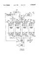
- the circuit 10generally comprises an external circuit 12, a clocking circuit 14 and an external circuit 16.
- the external circuit 12can be operating at any particular frequency desired and the external circuit 16 can be operating at any other particular frequency desired.
- the frequency of the external circuit 12can even be the same as the frequency as the external circuit 16.
- the clocking circuit 14acts as a frequency converter from the frequency of the external circuit 12 to the frequency of the external circuit 16. If the frequency of the external circuit 12 is faster than the frequency of the external circuit 16, the clocking circuit 14 buffers the additional words until the external circuit 16 is capable of receiving them.
- the clocking circuit 14buffers words and then presents them to the external circuit 16 at a frequency that can be accommodated.
- the clocking circuit 14generally comprises a data input 42, a write counter 44, a set of decoder and multiplexers 46a, 46b, 46c and 46d, a set of memory arrays 48a, 48b, 48c and 48d, a set of sense amplifiers 50a, 50b, 50c and 50d, a read counter 52, and a data output 54.
- Each of the decoder and multiplexers 46a-46dhave a write timing input 56a-56d and a signal input 58a-58d.
- the write timing inputs 56a-56d of each of the decoder and multiplexers 46a-46dreceive a write timing signal from the write counter 44 when power is applied to the clocking circuit 14.
- the signal input 58a-58d of each of the decoder and multiplexers 46a-46dreceive a digital word from the data input 42 when power is applied to the clocking circuit 14.
- One or more of the decoder and multiplexers 46a-46dwrites a digital word to the corresponding memory array 48a-48d when a particular timing signal is received at the appropriate write timing input 56a-56d.
- the write timing input 56a-56d of each of the decoder and multiplexers 46a-46dis received through a timing bus 64.
- the decoder and multiplexers 46a-46dact as receiving devices which provide a means for receiving data and preferably sending the data to a memory device, such as a decoder, a decoder and multiplexer or other device(s) providing equivalent function(s).
- Each of the sense amplifiers 50a-50dhas a signal input 60a-60d and a read timing input 62a-62d. Each of the sense amplifiers 50a-50d is capable of receiving a digital word from the corresponding memory array 48a-48d when power is applied to the timing circuit 14. Each of the read timing inputs 62a-62d of the sense amplifiers 50a-50d receive a read timing signal from the read counter 52 when power is applied to the timing circuit 14. One or more of the sense amplifiers 50a-50d presents a signal to the data output 54 when an appropriate read timing signal is received at one of the read timing inputs 62a-62d. The read timing input 62 of each of the sense amplifiers 50a-50d is received from the read counter 52 through a timing bus 66.
- the sense amplifiers 50a-50dcan also be implemented as a latch or other output device that has a similar operation. Specifically, the sense amplifiers 50a-50d can be any output device that receives data from memory arrays 48a-48d by sensing a potential present, and possibly, but not necessary, amplifying the potential.
- the detailed workings of the word conversion of the clocking circuit 14are described in copending application Ser. No. 08/621,487, (Attorney Reference No. 64,663-037). Additional components to produce the frequency conversion include a clock 68, a write enable 70 and a read enable 72.
- the clock 68can be an externally supplied clock.
- the clock 68presents a reference clock to an input 74 of the write counter 44 as well as to an input 76 of the read counter 52.
- the write enable 70is presented to an enable input 78 of the write counter 44.
- the read enable 72is presented to an enable input 80 of the read counter 52.
- the write enable 70 and the read enable 72provide additional wait states necessary to compensate for the word width conversion performed by the clocking circuit 14. For example, if the data input 42 presents a stream of 9-bit digital words to the memory arrays 48a-48d and the data output receives a series of 18-bit digital words from the memory arrays 48a-48d, the write enable 70 and the read enable 72 must provide a 2-to-1 compensation. Specifically, the write enable 70 must be enabled on two clock cycles for every one clock cycle that the read enable 72 is enabled. Both the write enable 70 and the read enable 72 can be user supplied inputs. The write enable 70 and the read enable 72 also can be, but are not limited to, internally generated signals.
- the frequency of the read enable 72is one-half the frequency of the write enable 70, the 2-to-1 ratio of compensation is provided. Essentially, the read enable 72 is adding one additional wait state per read cycle of the clocking circuit 14. The ratio of the compensation provided by the write enable 70 and the read enable 72 is further illustrated by the following TABLE 1:
- FIG. 3further comprises a frequency shifter 90.
- the frequency shifter 90has an input that is received from the clock 68 and an output 94 that presents a manipulated clock signal to the input 76 of the read counter 52.
- the write enable 70 and the read enable 72are normally in an active state.
- the write enable 70 and the read enable 72are not variable frequency enable signals as shown in the FIG. 2 embodiment, but rather are either enabled or not enabled in a steady state condition.
- the frequency shifter 90provides the compensation for the multiple width digital words as illustrated in the TABLE 1.
- the frequency shifter 90divides the clock 68 by two and presents this reduced frequency clock at the input 76 of the read counter 52.
- the number of clocks required to produce the various frequenciescan be reduced.
- the clock 68may drive both the write counter 44 and the read counter 52.
- the write enable 70 and the read enable 72may be connected to an additional logic to prevent overrunning and underrunning of the memory arrays 48a-48d. Such additional logic is described in co-pending application Ser. No. 08/567,893, incorporated herein by reference in its entirety.
- the timing clock 100has a pulse 102, a pulse 104 and a pulse 106. On the leading edge of the pulse 102, 104 and 106 a digital word is read from the memory arrays 48a-48d. On the falling edge of the pulse 102, 104 and 106, a digital word is written to the memory arrays 48a-48d.
- the clocking circuit 14can be used for both synchronous and asynchronous applications.
- the clock inputmay have a read/write pin so that when the function is enabled the clocking circuit 14 can write asynchronously.
- the read/write pinis one example of operating the clocking circuit 14 in both synchronous and asynchronous applications.
- a timing clock 100is shown illustrating the write/read function of the clocking circuit 14 as well as the counter incrementing function of the clocking circuit 14. Since the write counter 44 and the read counter 52 are not in the speed path of the writing or reading of the memory arrays 48a-48d, the counters can be incremented on the opposite pulse of the clock cycle as the read or write operations are executed. For example, a positive pulse 110 illustrates when the write and read functions are implemented, while a negative pulse 112 illustrates when the counters are incremented. This allows one half of each clock cycle to decode the write timing signal at the decoder and multiplexers 46-46d. Similarly, one half of each clock cycle may decode the read timing signal at the sense amplifiers 50a-50d.
- the half cycle decodingis efficiently implemented. This half cycle decoding is a particular advantage when implementing circuits that run very fast (e.g., greater than 100 MHz).
- the present inventionmay be implemented as a data interface between systems which exchange data of the same or different bit sizes at the same or different rate.
- Such systemsmay include, but are not limited to, a network gateway, a modem, a facsimile machine, a disk drive buffer, a peripheral-computer interface, etc.
Landscapes
- Engineering & Computer Science (AREA)
- Theoretical Computer Science (AREA)
- Physics & Mathematics (AREA)
- General Engineering & Computer Science (AREA)
- General Physics & Mathematics (AREA)
- Dram (AREA)
Abstract
Description
TABLE 1 ______________________________________ SIZE OF SIZE OF FREQUENCY WORDS WORDS COMPENSATION READ WRITTEN READ ENABLE/WRITE ENABLE ______________________________________ 9-BIT 18-BIT .5 9-BIT 36-BIT .25 18-BIT 9-BIT 2 36-BIT 9-BIT 4 ______________________________________
Claims (24)
Priority Applications (1)
| Application Number | Priority Date | Filing Date | Title |
|---|---|---|---|
| US08/620,812US5764967A (en) | 1996-03-29 | 1996-03-29 | Multiple frequency memory array clocking scheme for reading and writing multiple width digital words |
Applications Claiming Priority (1)
| Application Number | Priority Date | Filing Date | Title |
|---|---|---|---|
| US08/620,812US5764967A (en) | 1996-03-29 | 1996-03-29 | Multiple frequency memory array clocking scheme for reading and writing multiple width digital words |
Publications (1)
| Publication Number | Publication Date |
|---|---|
| US5764967Atrue US5764967A (en) | 1998-06-09 |
Family
ID=24487497
Family Applications (1)
| Application Number | Title | Priority Date | Filing Date |
|---|---|---|---|
| US08/620,812Expired - LifetimeUS5764967A (en) | 1996-03-29 | 1996-03-29 | Multiple frequency memory array clocking scheme for reading and writing multiple width digital words |
Country Status (1)
| Country | Link |
|---|---|
| US (1) | US5764967A (en) |
Cited By (13)
| Publication number | Priority date | Publication date | Assignee | Title |
|---|---|---|---|---|
| US5978307A (en)* | 1998-05-21 | 1999-11-02 | Integrated Device Technology, Inc. | Integrated circuit memory devices having partitioned multi-port memory arrays therein for increasing data bandwidth and methods of operating same |
| US5982700A (en)* | 1998-05-21 | 1999-11-09 | Integrated Device Technology, Inc. | Buffer memory arrays having nonlinear columns for providing parallel data access capability and methods of operating same |
| US5999478A (en)* | 1998-05-21 | 1999-12-07 | Integrated Device Technology, Inc. | Highly integrated tri-port memory buffers having fast fall-through capability and methods of operating same |
| US6173425B1 (en) | 1998-04-15 | 2001-01-09 | Integrated Device Technology, Inc. | Methods of testing integrated circuits to include data traversal path identification information and related status information in test data streams |
| US6216205B1 (en) | 1998-05-21 | 2001-04-10 | Integrated Device Technology, Inc. | Methods of controlling memory buffers having tri-port cache arrays therein |
| US6240031B1 (en) | 2000-03-24 | 2001-05-29 | Cypress Semiconductor Corp. | Memory architecture |
| US6400642B1 (en) | 2000-03-24 | 2002-06-04 | Cypress Semiconductor Corp. | Memory architecture |
| US6526470B1 (en) | 1998-09-28 | 2003-02-25 | Cypress Semiconductor Corp. | Fifo bus-sizing, bus-matching datapath architecture |
| US6546461B1 (en) | 2000-11-22 | 2003-04-08 | Integrated Device Technology, Inc. | Multi-port cache memory devices and FIFO memory devices having multi-port cache memory devices therein |
| US6675329B1 (en)* | 1999-04-03 | 2004-01-06 | Lg Electronics Inc. | Internal memory in application specific integrated circuit device and method for testing internal memory |
| US20050152204A1 (en)* | 2004-01-14 | 2005-07-14 | Shih-Ked Lee | Multi-port memory cells for use in FIFO applications that support data transfers between cache and supplemental memory arrays |
| US20060155927A1 (en)* | 2003-07-02 | 2006-07-13 | Sergei Sawitzki | Single memory with multiple shift register functionality |
| US20090029748A1 (en)* | 2004-02-10 | 2009-01-29 | P & Tel Inc. | Sliding mechanism apparatus and appliance integrated with the same |
Citations (35)
| Publication number | Priority date | Publication date | Assignee | Title |
|---|---|---|---|---|
| US4467443A (en)* | 1979-07-30 | 1984-08-21 | Burroughs Corporation | Bit addressable variable length memory system |
| JPS6413996A (en)* | 1987-07-06 | 1989-01-18 | Nogyo Seibutsu Idenshi Kouzou | Gene capable of coding 3a protein of cucumber mosaic virus |
| US4802122A (en)* | 1987-04-28 | 1989-01-31 | Advanced Micro Devices, Inc. | Fast flush for a first-in first-out memory |
| US4839866A (en)* | 1987-05-29 | 1989-06-13 | Texas Instruments Incorporated | Cascadable first-in, first-out memory |
| US4864543A (en)* | 1987-04-30 | 1989-09-05 | Texas Instruments Incorporated | First-in, first-out memory with counter address pointers for generating multiple memory status flags |
| US4875196A (en)* | 1987-09-08 | 1989-10-17 | Sharp Microelectronic Technology, Inc. | Method of operating data buffer apparatus |
| US4876670A (en)* | 1986-12-10 | 1989-10-24 | Mitsubishi Denki Kabushiki Kaisha | Variable delay circuit for delaying input data |
| US4891788A (en)* | 1988-05-09 | 1990-01-02 | Kreifels Gerard A | FIFO with almost full/almost empty flag |
| US4985867A (en)* | 1988-09-14 | 1991-01-15 | Kawasaki Steel Corporation | Semiconductor memory circuit |
| US5084837A (en)* | 1988-01-22 | 1992-01-28 | Sharp Kabushiki Kaisha | Fifo buffer with folded data transmission path permitting selective bypass of storage |
| US5088061A (en)* | 1990-07-24 | 1992-02-11 | Vlsi Technology, Inc. | Routing independent circuit components |
| US5220529A (en)* | 1990-08-20 | 1993-06-15 | Fujitsu Limited | One-chip first-in first-out memory device having matched write and read operations |
| US5222047A (en)* | 1987-05-15 | 1993-06-22 | Mitsubishi Denki Kabushiki Kaisha | Method and apparatus for driving word line in block access memory |
| US5228002A (en)* | 1991-04-26 | 1993-07-13 | Quality Semiconductor Inc. | First-in first-out memory device and method for accessing the device |
| US5262996A (en)* | 1991-08-27 | 1993-11-16 | Industrial Technology Research Institute | FIFO module |
| US5265063A (en)* | 1990-07-16 | 1993-11-23 | Nec Corporation | Semiconductor memory device having a plurality of SRAMs operable in synchronism with a clock permitting simultaneous access to multiple data |
| JPH0676559A (en)* | 1992-06-26 | 1994-03-18 | Mitsubishi Electric Corp | First-in first-out memory device |
| US5305253A (en)* | 1985-06-20 | 1994-04-19 | Texas Instruments Incorporated | Zero fall-through time asynchronous fifo buffer with nonambiguous empty-full resolution |
| US5311475A (en)* | 1991-04-26 | 1994-05-10 | Quality Semiconductor Inc. | High speed full and empty flag generators for first-in first-out memory |
| US5317756A (en)* | 1987-10-20 | 1994-05-31 | Sharp Kabushiki Kaisha | Data processor for detecting identical data coexisting in a plurality of data section of data transmission paths |
| US5345419A (en)* | 1993-02-10 | 1994-09-06 | At&T Bell Laboratories | Fifo with word line match circuits for flag generation |
| US5367486A (en)* | 1991-01-07 | 1994-11-22 | Mitsubishi Denki Kabushiki Kaisha | Semiconductor memory device capable of correctly and serially reading stored data signals |
| US5404332A (en)* | 1993-10-07 | 1995-04-04 | Fujitsu Limited | Apparatus for and a method of detecting a malfunction of a FIFO memory |
| US5406273A (en)* | 1991-05-14 | 1995-04-11 | Sharp Kabushiki Kaisha | Data processor |
| US5406554A (en)* | 1993-10-05 | 1995-04-11 | Music Semiconductors, Corp. | Synchronous FIFO having an alterable buffer store |
| US5412611A (en)* | 1992-03-17 | 1995-05-02 | Fujitsu, Limited | FIFO memory device capable of writing contiguous data into rows |
| US5426612A (en)* | 1988-09-08 | 1995-06-20 | Hitachi, Ltd. | First-in first-out semiconductor memory device |
| US5467319A (en)* | 1993-09-20 | 1995-11-14 | Codex, Corp. | CAM array and method of laying out the same |
| US5471632A (en)* | 1992-01-10 | 1995-11-28 | Digital Equipment Corporation | System for transferring data between a processor and a system bus including a device which packs, unpacks, or buffers data blocks being transferred |
| US5490257A (en)* | 1992-02-24 | 1996-02-06 | Advanced Micro Devices, Inc. | RAM based FIFO memory half-full detection apparatus and method |
| US5506815A (en)* | 1995-01-19 | 1996-04-09 | Etron Technology Inc. | Reconfigurable multi-user buffer memory particularly for signal processing system |
| US5506809A (en)* | 1994-06-29 | 1996-04-09 | Sharp Kabushiki Kaisha | Predictive status flag generation in a first-in first-out (FIFO) memory device method and apparatus |
| US5513318A (en)* | 1994-12-28 | 1996-04-30 | At&T Corp. | Method for built-in self-testing of ring-address FIFOs |
| US5528553A (en)* | 1993-10-01 | 1996-06-18 | Hal Computer Systems, Inc. | Method and apparatus for testing random access memory |
| US5546347A (en)* | 1994-07-22 | 1996-08-13 | Integrated Device Technology, Inc. | Interleaving architecture and method for a high density FIFO |
- 1996
- 1996-03-29USUS08/620,812patent/US5764967A/ennot_activeExpired - Lifetime
Patent Citations (38)
| Publication number | Priority date | Publication date | Assignee | Title |
|---|---|---|---|---|
| US4467443A (en)* | 1979-07-30 | 1984-08-21 | Burroughs Corporation | Bit addressable variable length memory system |
| US5305253A (en)* | 1985-06-20 | 1994-04-19 | Texas Instruments Incorporated | Zero fall-through time asynchronous fifo buffer with nonambiguous empty-full resolution |
| US4876670A (en)* | 1986-12-10 | 1989-10-24 | Mitsubishi Denki Kabushiki Kaisha | Variable delay circuit for delaying input data |
| US4802122B1 (en)* | 1987-04-28 | 1993-05-04 | Monolithic Memories Inc | |
| US4802122A (en)* | 1987-04-28 | 1989-01-31 | Advanced Micro Devices, Inc. | Fast flush for a first-in first-out memory |
| US4864543A (en)* | 1987-04-30 | 1989-09-05 | Texas Instruments Incorporated | First-in, first-out memory with counter address pointers for generating multiple memory status flags |
| US5222047A (en)* | 1987-05-15 | 1993-06-22 | Mitsubishi Denki Kabushiki Kaisha | Method and apparatus for driving word line in block access memory |
| US4839866A (en)* | 1987-05-29 | 1989-06-13 | Texas Instruments Incorporated | Cascadable first-in, first-out memory |
| JPS6413996A (en)* | 1987-07-06 | 1989-01-18 | Nogyo Seibutsu Idenshi Kouzou | Gene capable of coding 3a protein of cucumber mosaic virus |
| US4875196A (en)* | 1987-09-08 | 1989-10-17 | Sharp Microelectronic Technology, Inc. | Method of operating data buffer apparatus |
| US5317756A (en)* | 1987-10-20 | 1994-05-31 | Sharp Kabushiki Kaisha | Data processor for detecting identical data coexisting in a plurality of data section of data transmission paths |
| US5084837A (en)* | 1988-01-22 | 1992-01-28 | Sharp Kabushiki Kaisha | Fifo buffer with folded data transmission path permitting selective bypass of storage |
| US4891788A (en)* | 1988-05-09 | 1990-01-02 | Kreifels Gerard A | FIFO with almost full/almost empty flag |
| US5426612A (en)* | 1988-09-08 | 1995-06-20 | Hitachi, Ltd. | First-in first-out semiconductor memory device |
| US4985867A (en)* | 1988-09-14 | 1991-01-15 | Kawasaki Steel Corporation | Semiconductor memory circuit |
| US5265063A (en)* | 1990-07-16 | 1993-11-23 | Nec Corporation | Semiconductor memory device having a plurality of SRAMs operable in synchronism with a clock permitting simultaneous access to multiple data |
| US5088061A (en)* | 1990-07-24 | 1992-02-11 | Vlsi Technology, Inc. | Routing independent circuit components |
| US5220529A (en)* | 1990-08-20 | 1993-06-15 | Fujitsu Limited | One-chip first-in first-out memory device having matched write and read operations |
| US5367486A (en)* | 1991-01-07 | 1994-11-22 | Mitsubishi Denki Kabushiki Kaisha | Semiconductor memory device capable of correctly and serially reading stored data signals |
| US5228002A (en)* | 1991-04-26 | 1993-07-13 | Quality Semiconductor Inc. | First-in first-out memory device and method for accessing the device |
| US5311475A (en)* | 1991-04-26 | 1994-05-10 | Quality Semiconductor Inc. | High speed full and empty flag generators for first-in first-out memory |
| US5406273A (en)* | 1991-05-14 | 1995-04-11 | Sharp Kabushiki Kaisha | Data processor |
| US5262996A (en)* | 1991-08-27 | 1993-11-16 | Industrial Technology Research Institute | FIFO module |
| US5471632A (en)* | 1992-01-10 | 1995-11-28 | Digital Equipment Corporation | System for transferring data between a processor and a system bus including a device which packs, unpacks, or buffers data blocks being transferred |
| US5490257A (en)* | 1992-02-24 | 1996-02-06 | Advanced Micro Devices, Inc. | RAM based FIFO memory half-full detection apparatus and method |
| US5412611A (en)* | 1992-03-17 | 1995-05-02 | Fujitsu, Limited | FIFO memory device capable of writing contiguous data into rows |
| US5521876A (en)* | 1992-03-17 | 1996-05-28 | Fujitsu Limited | FIFO memory device capable of writing contiguous data into rows |
| JPH0676559A (en)* | 1992-06-26 | 1994-03-18 | Mitsubishi Electric Corp | First-in first-out memory device |
| US5375092A (en)* | 1992-06-26 | 1994-12-20 | Mitsubishi Denki Kabushiki Kaisha | First-in first-out memory device |
| US5345419A (en)* | 1993-02-10 | 1994-09-06 | At&T Bell Laboratories | Fifo with word line match circuits for flag generation |
| US5467319A (en)* | 1993-09-20 | 1995-11-14 | Codex, Corp. | CAM array and method of laying out the same |
| US5528553A (en)* | 1993-10-01 | 1996-06-18 | Hal Computer Systems, Inc. | Method and apparatus for testing random access memory |
| US5406554A (en)* | 1993-10-05 | 1995-04-11 | Music Semiconductors, Corp. | Synchronous FIFO having an alterable buffer store |
| US5404332A (en)* | 1993-10-07 | 1995-04-04 | Fujitsu Limited | Apparatus for and a method of detecting a malfunction of a FIFO memory |
| US5506809A (en)* | 1994-06-29 | 1996-04-09 | Sharp Kabushiki Kaisha | Predictive status flag generation in a first-in first-out (FIFO) memory device method and apparatus |
| US5546347A (en)* | 1994-07-22 | 1996-08-13 | Integrated Device Technology, Inc. | Interleaving architecture and method for a high density FIFO |
| US5513318A (en)* | 1994-12-28 | 1996-04-30 | At&T Corp. | Method for built-in self-testing of ring-address FIFOs |
| US5506815A (en)* | 1995-01-19 | 1996-04-09 | Etron Technology Inc. | Reconfigurable multi-user buffer memory particularly for signal processing system |
Non-Patent Citations (4)
| Title |
|---|
| U.S. Serial No. 08/567,893 Filed Dec. 6, 1995 Attorney Docket No. 64,663 013 For: State Machine Design For Generating Empty and Full Flags In an Asynchronous FIFO.* |
| U.S. Serial No. 08/567,893--Filed Dec. 6, 1995--Attorney Docket No. 64,663-013 For: State Machine Design For Generating Empty and Full Flags In an Asynchronous FIFO. |
| U.S. Serial No. N/A Filed Mar. 25, 1996 Attorney Docket No. 64,663 037 For: A Clocking Scheme For Independently Reading and Writing Multiple Width Words From a Memory Array.* |
| U.S. Serial No. N/A--Filed Mar. 25, 1996--Attorney Docket No. 64,663-037 For: A Clocking Scheme For Independently Reading and Writing Multiple Width Words From a Memory Array. |
Cited By (17)
| Publication number | Priority date | Publication date | Assignee | Title |
|---|---|---|---|---|
| US6173425B1 (en) | 1998-04-15 | 2001-01-09 | Integrated Device Technology, Inc. | Methods of testing integrated circuits to include data traversal path identification information and related status information in test data streams |
| US5982700A (en)* | 1998-05-21 | 1999-11-09 | Integrated Device Technology, Inc. | Buffer memory arrays having nonlinear columns for providing parallel data access capability and methods of operating same |
| US5999478A (en)* | 1998-05-21 | 1999-12-07 | Integrated Device Technology, Inc. | Highly integrated tri-port memory buffers having fast fall-through capability and methods of operating same |
| US6216205B1 (en) | 1998-05-21 | 2001-04-10 | Integrated Device Technology, Inc. | Methods of controlling memory buffers having tri-port cache arrays therein |
| US5978307A (en)* | 1998-05-21 | 1999-11-02 | Integrated Device Technology, Inc. | Integrated circuit memory devices having partitioned multi-port memory arrays therein for increasing data bandwidth and methods of operating same |
| US6526470B1 (en) | 1998-09-28 | 2003-02-25 | Cypress Semiconductor Corp. | Fifo bus-sizing, bus-matching datapath architecture |
| US6675329B1 (en)* | 1999-04-03 | 2004-01-06 | Lg Electronics Inc. | Internal memory in application specific integrated circuit device and method for testing internal memory |
| US6240031B1 (en) | 2000-03-24 | 2001-05-29 | Cypress Semiconductor Corp. | Memory architecture |
| US6400642B1 (en) | 2000-03-24 | 2002-06-04 | Cypress Semiconductor Corp. | Memory architecture |
| US6546461B1 (en) | 2000-11-22 | 2003-04-08 | Integrated Device Technology, Inc. | Multi-port cache memory devices and FIFO memory devices having multi-port cache memory devices therein |
| US6754777B1 (en) | 2000-11-22 | 2004-06-22 | Integrated Device Technology, Inc. | FIFO memory devices and methods of operating FIFO memory devices having multi-port cache memory devices therein |
| US6874064B2 (en) | 2000-11-22 | 2005-03-29 | Integrated Device Technology, Inc. | FIFO memory devices having multi-port cache and extended capacity memory devices therein with retransmit capability |
| US20060155927A1 (en)* | 2003-07-02 | 2006-07-13 | Sergei Sawitzki | Single memory with multiple shift register functionality |
| US7774573B2 (en)* | 2003-07-02 | 2010-08-10 | St-Ericsson Sa | Single memory with multiple shift register functionality |
| US20050152204A1 (en)* | 2004-01-14 | 2005-07-14 | Shih-Ked Lee | Multi-port memory cells for use in FIFO applications that support data transfers between cache and supplemental memory arrays |
| US7042792B2 (en) | 2004-01-14 | 2006-05-09 | Integrated Device Technology, Inc. | Multi-port memory cells for use in FIFO applications that support data transfers between cache and supplemental memory arrays |
| US20090029748A1 (en)* | 2004-02-10 | 2009-01-29 | P & Tel Inc. | Sliding mechanism apparatus and appliance integrated with the same |
Similar Documents
| Publication | Publication Date | Title |
|---|---|---|
| US5499344A (en) | Programmable dual port data unit for interfacing between multiple buses | |
| KR100337052B1 (en) | Dual port fifo with synchronized read and write pointers | |
| US5764967A (en) | Multiple frequency memory array clocking scheme for reading and writing multiple width digital words | |
| KR100915554B1 (en) | A semiconductor memory | |
| JP3645584B2 (en) | Data transfer synchronization device | |
| JP2000099193A (en) | Device and method for synchronization, and interface circuit | |
| US6816955B1 (en) | Logic for providing arbitration for synchronous dual-port memory | |
| JPH04301290A (en) | Pushup memory circuit | |
| US7016349B1 (en) | Logic for generating multicast/unicast address (es) | |
| US5117395A (en) | Expansible FIFO memory for accommodating added memory stages in a multistage memory with common control signals | |
| US8176353B2 (en) | Method for the data transfer between at least two clock domains | |
| US6148392A (en) | Low power implementation of an asynchronous stock having a constant response time | |
| US6701396B2 (en) | Data burst transfer circuit, parallel-serial and serial-parallel conversion circuits, and an oscillation circuit | |
| JP3571195B2 (en) | Host interface circuit of image forming apparatus | |
| JP3475857B2 (en) | Source synchronous transfer method | |
| US6510486B1 (en) | Clocking scheme for independently reading and writing multiple width words from a memory array | |
| JP4060270B2 (en) | Apparatus and method for delaying video line data between transmitter and receiver | |
| US6442657B1 (en) | Flag generation scheme for FIFOs | |
| US7899955B2 (en) | Asynchronous data buffer | |
| CN118734757B (en) | DDR physical layer interface circuit based on FPGA and control method thereof | |
| JP4193284B2 (en) | Elastic and integrated circuits | |
| JP2766006B2 (en) | Elastic store method | |
| JP2004185175A (en) | Fifo circuit for expansion and transmission-and-reception device | |
| EP0554731B1 (en) | Line interface for high-speed transmission line | |
| KR100313933B1 (en) | Data Transmission Control Apparatus |
Legal Events
| Date | Code | Title | Description |
|---|---|---|---|
| AS | Assignment | Owner name:CYPRESS SEMICONDUCTOR, CALIFORNIA Free format text:ASSIGNMENT OF ASSIGNORS INTEREST;ASSIGNOR:KNAACK, ROLAND T.;REEL/FRAME:007923/0381 Effective date:19960328 | |
| STCF | Information on status: patent grant | Free format text:PATENTED CASE | |
| FPAY | Fee payment | Year of fee payment:4 | |
| REMI | Maintenance fee reminder mailed | ||
| FPAY | Fee payment | Year of fee payment:8 | |
| REMI | Maintenance fee reminder mailed | ||
| FPAY | Fee payment | Year of fee payment:12 | |
| SULP | Surcharge for late payment | Year of fee payment:11 | |
| FEPP | Fee payment procedure | Free format text:PAYER NUMBER DE-ASSIGNED (ORIGINAL EVENT CODE: RMPN); ENTITY STATUS OF PATENT OWNER: LARGE ENTITY Free format text:PAYOR NUMBER ASSIGNED (ORIGINAL EVENT CODE: ASPN); ENTITY STATUS OF PATENT OWNER: LARGE ENTITY | |
| AS | Assignment | Owner name:CYPRESS SEMICONDUCTOR CORPORATION, CALIFORNIA Free format text:CONFIRMATORY ASSIGNMENT. ASSIGNOR HEREBY CONFIRMS THE SELL, ASSIGN, AND TRANSFER TO CYPRESS SEMICONDUCTOR CORPORATION OF THE ENTIRE RIGHT, TITLE, AND INTEREST;ASSIGNOR:KNAACK, ROLAND T.;REEL/FRAME:026159/0349 Effective date:20110419 | |
| AS | Assignment | Owner name:SOKIA MGMT. LIMITED LIBILITY COMPANY, DELAWARE Free format text:ASSIGNMENT OF ASSIGNORS INTEREST;ASSIGNOR:CYPRESS SEMICONDUCTOR CORPORATION;REEL/FRAME:026329/0516 Effective date:20110406 | |
| AS | Assignment | Owner name:CALLAHAN CELLULAR L.L.C., DELAWARE Free format text:MERGER;ASSIGNOR:SOKIA MGMT. LIMITED LIABILITY COMPANY;REEL/FRAME:036711/0530 Effective date:20150827 |